solar photovoltaic technologies - department of energy ...chetan/lecture/lecture-34 spt-dec.pdf ·...
TRANSCRIPT

Solar Photovoltaic
Technologies
Prof. C.S. Solanki
Energy Systems Engineering
IIT Bombay
Lecture-34

8/1/2008 © IIT Bombay, C.S. Solanki Solar Photovoltaic Technologies 2
Contents
Brief summary of the previous lecture
Various Thin film solar cell technologies
Low temperature deposition
High temperature deposition
Solar cell structures

8/1/2008 © IIT Bombay, C.S. Solanki Solar Photovoltaic Technologies 3
Classification of different approaches
• A large number of different technologies are under parallel
development
• A classification can be made based on different criteria:
• According to Tmax during layer formation
• According to grain size
• According to cell structure
•The R&D on the high-temperature routes is mainly driven
by considerations from classical bulk Si cells
Proven high efficiency and stability
• The R&D on the low-temperature routes is mainly driven
by considerations from a-Si:H solar cells
low thermal budget processing

8/1/2008 © IIT Bombay, C.S. Solanki Solar Photovoltaic Technologies 4
Crystalline Si films: deposition
temperature200 400 600 800 1000 1200 1400
Kaneka
PECVD
Sanyo
SPC
Canon
VHF-
PECVD
ECN
LPE
IMEC,
CNRS-PHASE
CVD
ISE,
MITSUBISHI
ZMR + CVD
Neuchâtel,
Jülich
VHF-
PECVD
•
(oC)
• Low temperature deposition :
micro-crystalline Si ( g <1000 nm)
• Medium temperature deposition:
poly–Si ( g <100 m)
• High temperature deposition :
multi-crystalline Si, mono-Si
Grain size vs Voc,with SRV
107 cm/s
103cm/s

8/1/2008 © IIT Bombay, C.S. Solanki Solar Photovoltaic Technologies 5
Crystalline Si materials
Type of Silicon AbbreviationCrystal Size
Range
Deposition
Method
Single-crystal
silicon
sc-Si >10cm Czochralski,
float zone
Multicrystalline
silicon
mc-Si 1mm-10cm Cast, sheet,
ribbon
Polycrystalline
silicon
pc-Si 0.1mm-1mm Chemical-vapor
deposition
Microcrystalline
silicon
mc-Si <0.1mm Ex: Plasma
deposition
• Thin film solar cell technologies requires a suitable substrate, and ……..

8/1/2008 © IIT Bombay, C.S. Solanki Solar Photovoltaic Technologies 6
Basic components of crystalline Si solar
cells
Substrate
Active layer, 5 to
50 m
EmitterARC
Diffusion
barrier
•Base contact, if substrate is
conductive
• Substrate can be non-conductive, in that case both
the contact is taken from the front side

8/1/2008 © IIT Bombay, C.S. Solanki Solar Photovoltaic Technologies 7
Solar cell structures
p-type
n-type
1. Homo-junction solar cell
for instance Mono-crystalline and multi-cystalline Si solar cells
p-type
n-type
2. Hetero-junction solar cell•p-type and n-type are different material
• more material choices some material can either be p-type or n-type
• used for material (thin-films) that absorbs light better than Si
• low series resistance window layer can be heavily doped
• CdTe and CIS are the examples
• in CdTe cell, CdS is used as window layer

8/1/2008 © IIT Bombay, C.S. Solanki Solar Photovoltaic Technologies 8
Solar cell structures
i-layer
n-type
p-type
3. p-i-n / n-i-p solar cell
• Based on drift rather than diffusion
• Absorption take place in thicker intrinsic layer
• p-type a-Si / int a-Si / n-type a-Si
4. Multijunction solar cell
•Also called Tandem cells
•Can acieve high efficiency by capturing larger part of the spectrum
• individual cells with different bandgaps are stacked on top of one another
• Mechanically stacked and Monolithic
Eg1 > Eg2 > Eg3
Eg1
Eg2
Eg3

8/1/2008 © IIT Bombay, C.S. Solanki Solar Photovoltaic Technologies 9
Diffusion vs drift in thin films
i
bidrift
L
VEL
q
kTDLdiff
High quality Crystalline-Si uses p-n junction
Carrier are transported by diffusion to the junction large
diffusion length
junction is very thin
diffdrift LL *10
Low-quality material should use p-i-n structure
Diffusion length are small
Drift length is about 10 times greater than diffusion length
intrinsic layer is thicker

8/1/2008 © IIT Bombay, C.S. Solanki Solar Photovoltaic Technologies 10
Light trapping
• "light trapping" in which the optical path length is several times the
actual device thickness
• Light trapping is usually achieved by changing the angle at which light
travels in the solar cell
• texturing reduces reflection and increases optical path length
Following schemes are used for light trapping
2211 sinsin nnSnell’s law
substrate substrate substrate

8/1/2008 © IIT Bombay, C.S. Solanki Solar Photovoltaic Technologies 11
Deposition techniques
• Physical vapor deposition
–Vacuum evaporation
–Sputtering
• Chemical deposition
– Chemical vapor deposition
(CVD)
– Hot wire CVD
– Plasma enhanced CVD
– Electro-deposition
– Spray pyrolysis
• Liquid phase deposition
– Liquid phase epitaxy

8/1/2008 © IIT Bombay, C.S. Solanki Solar Photovoltaic Technologies 12
Contents
• Motivation
• Different thin-film solar cell technologies
• Why crystalline Si films?
• Classification based on grain size
• Thin-film solar cell structures
• Deposition techniques
• low temperature
• High temperature approaches
Mono-crystalline Si thin films
• Other concepts

8/1/2008 © IIT Bombay, C.S. Solanki Solar Photovoltaic Technologies 13
Low-temperature approaches
Property
Deposition temperature 200 – 550oC
Deposition technologies Plasma-enhanced (PECVD, VHF-PECVD,
microwave, ECR)
Hot-wire CVD
Solid Phase crystallisation of a-Si:H
Si-precursor SiH4
Dilution with H2 is necessary for PECVD
microcrystalline Si
Deposition rate 0.1 –1 nm/s
1 nm/s (Kaneka), mostly below 0.5 nm/s
Cell structure Mostly p-i-n
Dual junction: Micromorph

8/1/2008 © IIT Bombay, C.S. Solanki Solar Photovoltaic Technologies 14
Low-temperature processes
Technology Main R&D-players Features / results
PECVD
VHF-PECVD
IPV-Juelich
Neuchatel
(VHF-Technologies)
Kaneka Solartech
Pacific Solar
Systems (13.56, 27.12, 40.28 MHz, 4-
chamber, 6-chamber system, 30x30 cm2)
Micromorph cell: > 13%
Micromorph cell: 12%
Module: 9%
Micromorph cell: 14.5%
Micromorph module: 10%
Module (30x30 cm2): 7%
!p-n polycrystalline Si solar cell!
Hot-wire CVD University Utrecht
IPV-Juelich
Micromorph cell on stainless steel: 8%
Solid Phase
crystallisation
Sanyo Staring from n+-a-Si:H/a-Si:H-layer
With p+-a-Si:H HIT-emitter: 9.2%
8/1/2008 © IIT Bombay, C.S. Solanki Solar Photovoltaic Technologies 15
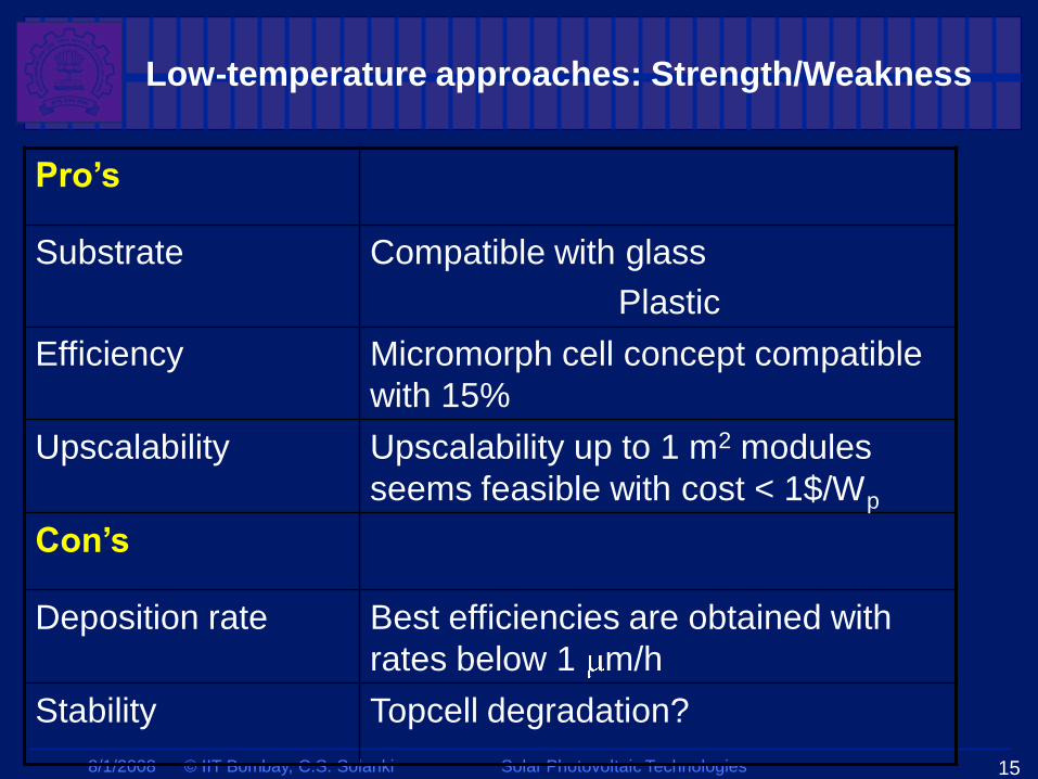
Low-temperature approaches: Strength/Weakness
Pro’s
Substrate Compatible with glass
Plastic
Efficiency Micromorph cell concept compatible
with 15%
Upscalability Upscalability up to 1 m2 modules
seems feasible with cost < 1$/Wp
Con’s
Deposition rate Best efficiencies are obtained with
rates below 1 m/h
Stability Topcell degradation?

8/1/2008 © IIT Bombay, C.S. Solanki Solar Photovoltaic Technologies 16
Low temperature deposition:
c-Si films
Features
•Grain size ~ 100nm
• Temperature < 600 C
• Small Minority carrier diffusion length
< I micron
• P-I-N structure,
• ~ 10 %
Deposition techniques
• Solid phase crystallization
• Plasma enhanced CVD
• Hot wire CVD
• Sputtering +
Metal induced crystallization
Substrates
• glass
• SnO2/ZnO coated glass
• metal : stainless steel
Back contact
c-Si i layer
front contactTCO
Glass/metal
n layer
p layer

8/1/2008 © IIT Bombay, C.S. Solanki Solar Photovoltaic Technologies 17
High-temperature approaches
Property
Deposition temperature 900 – 1300oC
Deposition technologies CVD
Solution Growth
Electrodeposition
Chemical Vapor Transport (CVT)
IMEC, PHASE
ECN, Stuttgart
NREL
NREL
Si-precursor SiH4, SiH2Cl2, SiHCl3
Deposition rate 1 – 10 m/min
Cell structure Always p-n Epitaxial cells
Interdigitated cells on
non-conductive
substrate

8/1/2008 © IIT Bombay, C.S. Solanki Solar Photovoltaic Technologies 18
Technology Main R&D-players Features / results
CVD
RTCVD
Continuous CVD
IMEC, ISE,
Stuttgart
PHASE
ISE
Monocrystalline epitaxial cells: 17.8%
Multicrystalline epitaxial cells: 14%
Polycrystalline Si solar cells: 6%
Chemical Vapor
Transport
NREL Based on iodine as transporting agent
Efficiency < 2%
Solution Growth /
Liquid Phase
Epitaxy
MPI-Stuttgart
ECN
UNSW
ANU
Monocrystalline epitaxial cells: 17.4%
Multicrystalline epitaxial cells: 15%
Electrodeposition NREL Made from molten salts of Si
High-temperature approaches

8/1/2008 © IIT Bombay, C.S. Solanki Solar Photovoltaic Technologies 19
High-temperature approaches
Pro’s
Substrate Compatible with Si (perfect match of TEC)
Efficiency High efficiency proven with epitaxial concept
Homogeneity/
reproducibility
Large expertise from microelectronics available
Doping and thickness homogeneity < 5%
Con’s
Substrate Only high-temperature resistant substrates: Si, ceramics,
glass-ceramics
Strong requirements on TEC-match and purity
Blocking layers
Efficiency Non-recrystallised polycrystalline Si-layers on ceramic suffer
from low efficiency
Upscalability High-throughput concepts are available but not proven

8/1/2008 © IIT Bombay, C.S. Solanki Solar Photovoltaic Technologies 20
Pro’s
Efficiency High efficiency proven
10.5% on Si:SiC, 8-9% on mullite, SiN,
Homogeneity/
reproducibility
Because of the extreme conditions, small deviations during
recrystallisation (thickness of ceramic, change in thermal
properties) can lead to unstable solidification and increased
defect densities
Con’s
Substrate Only very high-temperature resistant substrates: Si, SiN, mullite,
Al2O3
Very strong requirements on TEC-match and purity
Thick blocking layers
Process Rather complex process ( 4 additional steps to realise active
layer on ceramic)
Upscalability Quality of Si-layers, subjected to ZMR, decreases at
recrystallisation speeds above 10 cm/min
Zone Melting Recrystallisation

8/1/2008 © IIT Bombay, C.S. Solanki Solar Photovoltaic Technologies 21
High temperature deposition:
Poly-Si films
Features
Grain size up to ~ several microns
• Temperature > 600 C
• diffusion length ~ 10s of microns
• P-N structure,
• ~ 11 %
Deposition techniques:
• Thermal CVD
• Ion assisted deposition
• Liquid phase epitaxy
(Zone melting recrystallization)
Substrate requirements
• Cost-effective
• Heat resistant
• Chemically inert
• Thermal expansion co-efficient matching
• Substrates: Alumina, mullite, graphite, low-cost Si
• Diffusion barrier: SiC, oxide/nitride
Back contact
Front contactARC
Epi-Si filmp+
p
n+
Ceramic substrate
Diffusion barrier
CVD si layer
Conducting substrate

8/1/2008 © IIT Bombay, C.S. Solanki Solar Photovoltaic Technologies 22
Monocrystalline Si thin films
• Best possible thin-film solar cell performance
• Thin mc-Si films are obtained using “Layer transfer processes”
Starting substrate is a Si wafer
surface conditioning for forming separation layer
thin-film transfer to a foreign substrate
recycling of starting Si substrate
Device fabrication
How to form a separation layer?Example-2
Intermediate Oxide layer Example-1
Hydrogen implantation
Si
Si
Example-3
Porous Silicon layer
Si
Si

8/1/2008 © IIT Bombay, C.S. Solanki Solar Photovoltaic Technologies 23
Porous Silicon Layer Transfer
(PSLT)
PSLT processes
• ELTRAN (Canon, Japan)
• SPS (Sony, Japan)
• PSI (ZAE, Germany)
• QMS (IPE, Germany)
• LAST (IMEC, Belgium)
• FMS (IMEC, Belgium)
• High monocrystalline Si layer can be deposited.
• Substrate can be re-used several times.
Porous silicon serves two purposes
Pores
• Anodization of Si in HF results in the formation ofporous silicon, columns of Si etched out (p+ Si).
• Layer porosity is a function of anodization parameters.
What is porous silicon ?

8/1/2008 © IIT Bombay, C.S. Solanki Solar Photovoltaic Technologies 24
Integral Steps of PSLT
• Porous silicon formation
Silicon

8/1/2008 © IIT Bombay, C.S. Solanki Solar Photovoltaic Technologies 25
SiliconSilicon
Integral Steps of PSLT
• Porous silicon formation
• Active layer deposition
- Annealing
- CVD epitaxial layer

8/1/2008 © IIT Bombay, C.S. Solanki Solar Photovoltaic Technologies 26
Integral Steps of PSLT
• Porous silicon formation
• Active layer deposition
• Device fabrication
Silicon

8/1/2008 © IIT Bombay, C.S. Solanki Solar Photovoltaic Technologies 27
Integral Steps of PSLT
• Porous silicon formation
• Active layer deposition
• Device fabrication
• Layer separation and transfer to
foreign substrate
Silicon
Substrate

8/1/2008 © IIT Bombay, C.S. Solanki Solar Photovoltaic Technologies 28
Film Separation:
One-step anodization
Porous Silicon
Film
Silicon Substrate
Porous Silicon Film
20 m film
Features
• Homogeneous film thickness
• Film thickness from few microns to several tens of microns
• Film area is limited by experimental set up
• Film thickness is function anodization parameters
• Separation occurs for limited set of parameters
• US patent # 6649485

8/1/2008 © IIT Bombay, C.S. Solanki Solar Photovoltaic Technologies 29
Silicon ingot
Electrolyte
Pt electrode
Continuous production of films
• HF conc. resumes at the surface after film separation

8/1/2008 © IIT Bombay, C.S. Solanki Solar Photovoltaic Technologies 30
Silicon ingot
Pt electrode
Electrolyte
Continuous production of films
• HF conc. resumes at the surface after film separation

8/1/2008 © IIT Bombay, C.S. Solanki Solar Photovoltaic Technologies 31
Continuous production of films
Silicon ingot
Pt electrode
Electrolyte
Porous silicon
films
• HF conc. resumes at the surface after film separation
• Patent pending

8/1/2008 © IIT Bombay, C.S. Solanki Solar Photovoltaic Technologies 32
FMS cell process
Solar cell realization:
FMS (Freestanding Mono-Si) solar
cellsPS Film
Epitaxial layer
Epi layer after PS
removal
• Two-side contacted cell structure
PS Film
Epi layer
Emitter
0
0.2
0.4
0.6
0.8
1
400 600 800 1000 1200
Wavelength (nm)
IQE
FMS -1
FMS -2
Ref-20um
IQE analysis
0
5
10
15
20
25
30
35
0 0.2 0.4 0.6
Voltage (Volts)
Curr
ent
(mA
/cm
2) Voc: 602.6 Volts
Isc: 33.12 mA/cm2
FF: 60.18
Eff.: 12.01%
Area: 0.65 cm2
Film thickness: 20 m
I-V curve
• Patent pending
Device is ready
• 9.6% FMS cell with HIT emitter

8/1/2008 © IIT Bombay, C.S. Solanki Solar Photovoltaic Technologies 33
Other processes:
a-Si/c-Si hetero-junction
•This configuration has the following advantages:
• potential for high efficiency;
•low processing temperatures.
• low thermal budget for processing. Reduction of
energy pay back time;
• reduced cost of cell technology.
Epi layer, p-type
Epi layer, p+ type Al back contact
int. a-Si:H
n+, a-SiH
Front contactITO layer Combination of low
production cost of
amorphous cell
technology and high
efficiency of Mono-
crystalline Si cell
technology
Bandgaps: a-Si 1.7 to
1.8 eV, C-Si 1.12eV

8/1/2008 © IIT Bombay, C.S. Solanki Solar Photovoltaic Technologies 34
Other processes:
Aluminum induced crystallization• for growing polycrystalline silicon (poly-Si) films on inexpensive glass
• Films is formed by aluminum-induced crystallization (AIC) of amorphous
silicon (a-Si)
• Annealing transforms an initial glass/Al/a-Si stack into a glass/poly-
Si/Al(Si) below the eutectic temperature of the Al/Si system (Teu=577 °C).
•The poly-Si forms a continuous layer which consists of large grains with a
preferential (1 0 0) orientation
Al
a-Si
Glass
Al
crystalline-Si
Glass
annealing

8/1/2008 © IIT Bombay, C.S. Solanki Solar Photovoltaic Technologies 35
Conclusions
• Thin-film crystalline Si solar cells represent obvious way
to reduce costs PV
• A large number of techniques are under investigation
• There is a certain risk for subcritical R&D in this field
• Crucial issues are clear:
• Low-T techniques: increase of growth rate
• High-T techniques
• Availability of ceramic substrate
• Increase of recrystallisation speed for process
• Improvement of nucleation control for process
without ZMR
• On all of these questions there is a considerable R&D-activity

8/1/2008 © IIT Bombay, C.S. Solanki Solar Photovoltaic Technologies 36
Concentrator PV
systems

8/1/2008 © IIT Bombay, C.S. Solanki Solar Photovoltaic Technologies 37
Why solar concentrators?
• Replace expensive cell
material with cheaper material
• increased power output
per unit area
• Efficiency of solar cell increases under concentration
• Smaller area
solar cells are
easier to
manufacture
Solar cell
Concentration (suns)
Eff
icie
nc
y (
%)
Fil
l F
acto
r (%
)

8/1/2008 © IIT Bombay, C.S. Solanki Solar Photovoltaic Technologies 38
Components of CPV systems
Solar cell
Heat sink
1 - Light collector
2 – Solar Cell
3 – Heat Sink
4 – Sun tracker

8/1/2008 © IIT Bombay, C.S. Solanki Solar Photovoltaic Technologies 39
Light collectors
• Refraction and
reflection
• Concentration
ratio
•Line focus &
point focus
• Imaging & non-
imaging
concentrator

8/1/2008 © IIT Bombay, C.S. Solanki Solar Photovoltaic Technologies 40
Solar cells for concentrators•Single-junction solar cells & Multi-junctionsolar cells
0.5 1 1.5 2 2.5
Wavelength (µm)
0.5
1.0
1.5
Su
nli
gh
t in
ten
sit
y
(kW
/m2/
m)
Single-junction solar cell
• Si is mainly used for
solar cell
• Lowering series
resistance is main
design parameter
• Laser grooved buried
contact solar cells
• Limited in solar
cell efficiency

8/1/2008 © IIT Bombay, C.S. Solanki Solar Photovoltaic Technologies 41
Multi-junction solar cells• Bandgap engineering
• Materials are manipulated to adjust the bandgap according
to solar spectrum
• Double and triple-junction solar cells
• InGaP/GaAs/Ge on Ge substrate
0.5 1 1.5 2 2.5
Wavelength (µm)
0.5
1.0
1.5S
un
lig
ht in
ten
sit
y
(kW
/m2/
m)
Eg1 > Eg2 > Eg3
Eg1
Eg2
Eg3

8/1/2008 © IIT Bombay, C.S. Solanki Solar Photovoltaic Technologies 42
Multi-junction solar cells
- 37.3 % (concentration
@175 Suns, 2004) World
record efficiency by
Spectrolab
- 13% with 6 junction
• Bandgap GaInP2 - 1.89eV
GaAs – 1.42 eV
Ge – 0.67 eV
• Design challenge is to match current from
each cell
• Higher number of junction can achieve higher
efficacies 40% is target by 2006
• Potentially 45% by 2010 (Spectrolab)

8/1/2008 © IIT Bombay, C.S. Solanki Solar Photovoltaic Technologies 43
Comparison of technologies
Material t/ η Disadvantages Advantages, perspectives
Mono-Si
300
m,
15 -
18 %
Lengthy production
procedure, wafer
sawing necessary
Best researched solar cell
material in a next few years it
will dominate world market,
especially there, where
high power/area ratio is
required
Multi-c Si
300
m,
13 -
15 %
lengthier
production
procedure, wafer
sawing necessary
The most important
production procedure at
least for the next ten years
Polyc-Si
Transpare
nt
300
m,
10 %
Lower efficiency,
special procedures
to achieve optical
transparency
required
Attractive solar cells for different
BIPV applications. Possible
also production of double sided
cells

8/1/2008 © IIT Bombay, C.S. Solanki Solar Photovoltaic Technologies 44
Comparison of technologies
Material t / ηDisadvantage
sAdvantages, perspectives
EFG
250
m,
14 %
Limited use
of this
production
procedure
Very fast crystal growth, no
wafer sawing necessary,
significant decrease in production
costs possible in the future
Riboon-Si
300
m,
12 %
Limited use of
this production
procedure
No wafer sawing necessary,
significant decrease in production
costs possible in the future
a-Si
1 m,
5 - 8
%
Lower
efficiency,
shorter life
span.
No sawing necessary, possible
production in the flexible form. It
is a promising material in the
future if long-term stability
increases

8/1/2008 © IIT Bombay, C.S. Solanki Solar Photovoltaic Technologies 45
Comparison of technologies
Material t / ηDisadvanta
gesAdvantages, perspectives
CdTe
2-3 m ,
6 - 9 %
(mod.)
Poisonous
raw
materials
Significant decrease in
production costs possible in
the future
CIS
2-3 m,
7,5 -
9,5 %
(mod.)
Limited
Indium
supply in
nature
Significant decrease in
production costs possible in
the future
HIT 200 m,
18 %
Limited use
of this
production
procedure
Higher efficiency, better
temperature coefficient and
lower thickness.