solid state growth kinetics of complex …ycchan/publications-ycchan/...1-4244-0665-x/06/$20.00...
TRANSCRIPT

1-4244-0665-X/06/$20.00 ©2006 IEEE 211 2006 Electronic Packaging Technology Conference
Solid State Growth Kinetics of Complex Intermetallics in the Pb-free Ball Grid Array (BGA) Solder Joint for MEMS Packaging
M. O. Alam1 & 3, Yang Dan1, B. Y. Wu1, Y. C. Chan1 & *, L. Rufer2, C. Bailey3
1Department of Electronic Engineering, City University of Hong Kong, Kowloon Tong, Hong Kong 2TIMA Laboratory, 46 Av. Félix Viallet, 38 031 Grenoble, France
3CMS, University of Greenwich, London SE10 9LS, UK *E-mail: [email protected]
Abstract
Interfacial reaction and reliability related problems of the solder joint for both advanced electronic packaging applications and MEMS packaging applications are becoming crucial with the downscaling of the device size. In this study, the solid state interfacial reaction between the BGA Sn-3.5%Ag-0.5%Cu solder and the Au/Ni/Cu bond pad for MEMS applications was investigated at 150-200oC, for different time period ranging from 0 hrs to 400 hrs and compared with that of the Sn-3.5%Ag solder. We found that 0.5 wt% Cu addition plays a strong role on the interfacial reaction products and the reaction kinetics – especially, at a high temperature near the melting point of the solder alloy. While the Sn-3.5%Ag solder reacts with the Au/Ni/Cu metallization simply by forming only one binary intermetallic compound (BIMC), the Sn-3.5%Ag-0.5%Cu solder reacts in a completely different manner.
1. Introduction Reliable packaging is a major challenge for the growth
of MEMS applications. Packaging cost of the MEMS product is about 50-90% of the total cost, however, reliability of a MEMS package is still a persistence issue that need to be addressed. Ball Grid Array (BGA) soldering has become a well-accepted interconnection technology for most of the MEMS packaging because of its self-alignment capability and least parasitic characteristics [1-4]. Figure 1 depicts schematically a typical MEMS package architecture where BGA solder joint is used for the third level interconnection.
Figure 1 Schematic view of a MEMS package architecture showing the application of BGA solder joint for the third level interconnection.(courtesy: Dr. Hyman, XCOM Wireless, Inc.)
In the emerging Pb-free era, SnAg and SnAgCu solders have been suggested against conventional SnPb solder, while SnAgCu has been recommended to be the best choice [4, 5]. However, lots of interfacial reaction and reliability
related problems of this solder still unknown that might impair the functionality of an advanced electronic package and/or a MEMS package.
2. Experimental Area-array solder mask-defined copper bond pads on the
MEMS substrate were used as the base for electrodeposition of Ni and Au. The average thickness of Ni and Au were 4 µm and 0.5 µm, respectively. Commercially-available BGA solder balls of eutectic Sn-3.5%Ag (m.p. ≈ 221oC) and Sn-3.5%Ag-0.5%Cu (m.p. ≈ 217oC) were used to understand the solid state interfacial reaction of Pb-free BGA solder joint for MEMS packaging. The compositions are given in weight percent. The solder mask-opening diameter was 0.6 mm and the diameter of the BGA solder ball before melting was 0.76 mm. Commercial water-soluble flux was screen printed on the Au/Ni/Cu bond pad of the BGA substrate. Solder balls were placed on the pre-fluxed Au/Ni/Cu bond pads and reflowed in a N2 atmosphere oven. A schematic diagram of the soldering process on the BGA substrate was shown in reference 6. Solder balls of Sn-3.5%Ag and Sn-3.5%Ag-0.5%Cu were placed side by side to experience identical conditions of reaction. The peak reflow temperature was 240°C and the time above the melting point of the solders was about 0.5 minutes. Immediately after the reflow, the substrates were subjected to high temperature aging at 150oC, 175oC and 200oC for time up to 400 h. After aging test for each readout point, the cross-sectioned samples were prepared to study the interfacial microstructure with a Philips XL 40 FEG scanning electron microscope (SEM) equipped with energy dispersive X-ray analysis (EDX). The back-scattered electron (BSE) mode of SEM was used to examine the morphology of cross-sectioned samples and to measure intermetallic (IMC) thickness. The average thickness of an IMC layer was determined by measuring the layer thickness at 20 equally spaced points from each solder joint. At least 5 solder joints were used for a final average value.
3. Results and Discussions The microstructures of the as-reflowed interfaces of Sn-
3.5%Ag solder and Sn-3.5%Ag-0.5%Cu solder on the Au/Ni/Cu metallization are shown in Figure 2. For the Sn-Ag solder interface, simply Ni3Sn4 was formed, whereas, for the SnAgCu interface, the IMC is composed of Cu, Ni and Sn. Some protruded grains were also noticed at the SnAgCu interface.
Microstructures of the solder interface after solid state aging at each temperature for different times were carefully investigated. Because of the lower melting temperature of the solder alloys, most of the previous works on the aging of

212 2006 Electronic Packaging Technology Conference
solder joints were conducted up to 150oC [2]. However, in this study we were interested to find the ultimate solid-state reactions at very high homologous temperatures.
(a) Sn-3.5%Ag solder interface
(b) Sn-3.5%Ag-0.5%Cu solder interface
Figure 2 Microstructure of the as reflowed interface between Au/Ni/Cu bond pad and the lead-free solder of (a) Sn-3.5%Ag, and (b) Sn-3.5%Ag-0.5%Cu.
Figure 3 shows scanning electron micrographs of interfaces of Sn-3.5%Ag solder (a) and Sn-3.5%Ag-0.5%Cu solder (b) with the Au/Ni/Cu metallization after aging at 175oC for 300 hrs. Comparing with Sn-3.5%Ag solder interface, thicker IMC layer with huge voids/defect at the Sn-3.5%Ag-0.5%Cu solder interface is clearly visible. From the EDX analysis, it was found that the IMC formed at the Sn-3.5%Ag-0.5%Cu solder interface is rather complex that is incorporated with Cu, Ni and Sn. Comparing literature, we are confirmed that it is a ternary intermetallic compound (TIMC) of (Cu,Ni)6Sn5 which is based on binary intermetallic compound (BIMC) of Cu6Sn5. However, with prolong aging time, we have noticed other IMCs at the solder interface, namely (Ni,Cu)3Sn4 and Cu3Sn.
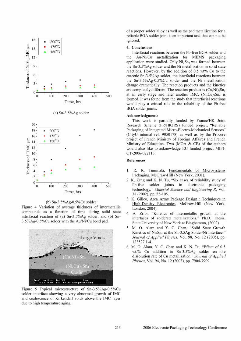
Figure 4 shows plots of the IMC thickness against the aging time at different temperatures. The differences between these two solders in IMC growth kinetics are very clear. For the Sn–3.5%Ag solder, the curves seem to be parabolic at the temperature range studied. However, from the trend of the curves at three different temperatures, it is clear that at higher temperatures, IMC growth rate is higher. Contrary to the Sn–3.5%Ag solder, Sn–3.5%Ag–0.5%Cu solder shows a peculiar growth kinetic. Although the growth is parabolic at 150oC temperature, it is questionable at higher temperature reaction. IMC growth curves for both
solders indicate that the common assumption of parabolic growth kinetics, i.e. n= 0.5 (bulk diffusion controlled growth kinetics), may not be applied for the SnAgCu solder at each aging temperature.
(a) Sn-3.5%Ag solder interface
(b) Sn-3.5%Ag-0.5%Cu solder interface
Figure 3 Scanning electron micrographs of (a) Sn-3.5%Ag solder, and (b) Sn-3.5%Ag-0.5%Cu solder interfaces after aging at 175oC for 300 hrs. (both figures are in the same magnification)
From the detailed microstructural studies conducted in this work, we have noticed cracks at the interface of the SnAgCu BGA solder joint on the Au/Ni/Cu metallization during high temperature aging. Because of the addition of the Cu the reaction products are different while due to the limited Cu content (0.5 wt%) in the BGA solder ball, the microchemistry of the reaction products and the kinetics are changing with time. In some location, very abnormal growth of (Cu,Ni)6Sn5 was noticed as shown in Figure 5. It is believed that this abnormal growth might be a result of faster diffusion of Cu and Sn from the IMC-solder interface to the IMC layer. Yet, more in-depth studies are needed to underpin the reason and the mechanism of the abnormal growth behavior. However, faster diffusion of the selective atoms results Kirkendal voids that collapse together to form a continuous cracks at the solder interface. Any crack at the interface would make the SnAgCu BGA solder joint unreliable for either MEMS packaging or advanced electronic packaging [4]. Thus, it is concluded that selection
Ni3Sn4
(Cu,Ni)6Sn5Cu-Ni-Sn
Ni3Sn4
(Cu,Ni)6Sn5
213 2006 Electronic Packaging Technology Conference
(a) Sn-3.5%Ag solder
(b) Sn-3.5%Ag-0.5%Cu solder Figure 4 Variation of average thickness of intermetallic compounds as a function of time during solid state interfacial reaction of (a) Sn-3.5%Ag solder, and (b) Sn-3.5%Ag-0.5%Cu solder with the Au/Ni/Cu bond pad.
Figure 5 Typical microstructure of Sn-3.5%Ag-0.5%Cu solder interface showing a very abnormal growth of IMC and coalescence of Kirkendall voids above the IMC layer due to high temperature aging.
of a proper solder alloy as well as the pad metallization for a reliable BGA solder joint is an important task that can not be ignored.
4. Conclusions Interfacial reactions between the Pb-free BGA solder and
the Au/Ni/Cu metallization for MEMS packaging application were studied. Only Ni3Sn4 was formed between the Sn-3.5%Ag solder and the Ni metallization in solid state reactions. However, by the addition of 0.5 wt% Cu to the eutectic Sn-3.5%Ag solder, the interfacial reactions between the Sn-3.5%Ag-0.5%Cu solder and the Ni metallization change dramatically. The reaction products and the kinetics are completely different. The reaction product is (Cu,Ni)6Sn5 at an early stage and later another IMC, (Ni,Cu)3Sn4 is formed. It was found from the study that interfacial reactions would play a critical role in the reliability of the Pb-free BGA solder joints.
Acknowledgments This work is partially funded by France/HK Joint
Research Scheme (FR/HKJRS) funded project, “Reliable Packaging of Integrated Micro-Electro-Mechanical Sensors” (CityU internal ref. 9050178) as well as by the Procore project of French Ministry of Foreign Affaires and French Ministry of Education. Two (MOA & CB) of the authors would also like to acknowledge EU funded project MIFI-CT-2006-022113.
References 1. R. R. Tummala, Fundamentals of Microsystems
Packaging, McGraw-Hill (New York, 2001). 2. K. Zeng and K. N. Tu, “Six cases of reliability study of
Pb-free solder joints in electronic packaging technology,” Material Science and Engineering R, Vol. 38 (2002), pp. 55-105.
3. K. Gilleo, Area Array Package Design : Techniques in High-Density Electronics, McGraw-Hill (New York, London, 2004).
4. A. Zribi, “Kinetics of intermetallic growth at the interfaces of soldered metallizations,” Ph.D. Thesis, State University of New York at Binghamton, (2002).
5. M. O. Alam and Y. C. Chan, “Solid State Growth Kinetics of Ni3Sn4 at the Sn-3.5Ag Solder/Ni Interface,” Journal of Applied Physics, Vol. 98, No. 12 (2005), pp. 123527:1-4.
6. M. O. Alam, Y. C. Chan and K. N. Tu, “Effect of 0.5 wt.% Cu addition in Sn-3.5%Ag solder on the dissolution rate of Cu metallization,” Journal of Applied Physics, Vol. 94, No. 12 (2003), pp. 7904-7909.
0 100 200 300 400 50002468
101214161820
Thic
knes
s of T
IMC
, µm
Time, hrs
200oC 175oC 150oC
(Cu,Ni)6Sn5
(Ni,Cu)3Sn4 Cu3Sn
Large Voids
0 100 200 300 400 5000
3
6
9
12
15
18
Thic
knes
s of N
i 3Sn4 IM
C, µ
m
Time, hrs
200oC 175oC 150oC