sopc soc),a case study
TRANSCRIPT


内容提要
• 本讲的目的:
– 介绍嵌入式系统;
– 了解SOPC的开发过程。

现代计算机系统


基于FPGA的嵌入式系统硬件平台

基于FPGA的嵌入式系统结构

FPGA support for embedded systems
• 硬件 – Processor core that can be instantiated on the FPGA
chip • Altera:基于Nios II微处理器的SOPC系统 • Xilinx:基于MicroBlaze微处理器的SOPC系统
– Memory modules and interfaces – I/O interfaces – Timer/counter circuits
• 软件 – CAD software tools for designing and implementing
a system

Nios processor
• 2000年,Altera发布了Nios处理器,这是第一款可
用于可编程逻辑器件的可配置的软核处理器。
– 基于RISC技术
– 16位指令集
– 16/32位数据通道
– 5级流水线
– 在一个时钟周期内完成一条指令的处理
– 具有一种基于JTAG的OCI(片上仪器)芯核
• 2004年,Altera继推出CycloneⅡ和StratrixⅡ器件
系列后,又推出支持这些芯片的NiosⅡ嵌入式处
理器。

Nios Ⅱ系列处理器的特性
种类 特 性
CPU结构
32Bit指令集
32Bit数据总线和地址总线2G Byte寻址空间
32个通用寄存器
32个中断源
片内调试 基于边界扫描测试(JTAG)的调试逻辑,支持硬件断点、数据触发以及片外和片内的调试跟踪
定制指令 最多达到256个用户定义的CPU指令
软件开发工具
NiosⅡIDE(集成开发环境)
基于GNU的编译器
硬件辅助的调试模块


Nios Ⅱ系列处理器的特性

Nios Ⅱ系列处理器的指令字

Example of a Nios Ⅱ Processor System

Altera CAD tools:Quartus II
• Quartus II:用于完成Nios II系统的综合、硬件优化、适配、编程下
载和硬件系统测试
– gate level,chip level,board level
• SOPC Builder:用于实现Nios II 系统的配置、生成
– 基于Nios II处理器的FPGA系统,不包括FPGA片外部分。
• Nios II IDE:用于软件开发、调试及运行
工程管理器;
编辑器和编译器;
调试器;
闪存编程器。
• ModelSim:用于对SOPC生成的Nios II 系统的HDL描述进行系统功能
仿真
• Matlab/DSP Builder——可生成Nios II 系统的硬件加速器

Nios Ⅱ嵌入式处理器软、硬件开发流程
SOPC Builder GUI
Connect Blocks
Processor Library Custom Instructions
Peripheral Library Select & Configure
Peripherals, IP
IP Modules
Configure Processor
Generate
EDIF Netlist
HDL Source Files
Testbench
Synthesis &
Fitter
User Design
Other IP Blocks
Hardware Development
Quartus II
On-Chip
Debug
Software Trace
Hard Breakpoints
SignalTap II
Altera
PLD
JTAG, Serial, or
Ethernet
Executable
Code
Hardware
Configuration
File Verification
& Debug
(1)
(2) (3)
(4)
C Header files
Custom Library
Peripheral Drivers
Compiler,
Linker, Debugger
Software Development
User Code
Libraries
RTOS
GNU Tools
Nios II IDE

硬件设计过程
硬件:
1. 创建一个Quartus Ⅱ工程
2. 创建Nios Ⅱ系统模块
① 启动SOPC Builder
② 添加CPU和外围器件
③ 指定基地址
④ 系统设置
⑤ 生成系统模块
3. 将Nios Ⅱ系统模块符号添加到BDF文
件中
4. 编译Quqrtus Ⅱ工程
5. 编程FPGA
软件:
启动Nios Ⅱ IDE;
1. 建立新的软件工程,编写源程序;
2. 编译工程;
3. 运行程序;
4. 调试程序;
5. 将程序下载到开发板上的Flash中。

Elements of the System Contents Tab

System designed using the SOPC Builder

系统生成
SDK使能
HDL使能
使能ModelSim
生成仿真文件
运行ModelSim 软件
系统生成过程
消息栏
SOPC Builder
消息栏

基于Linux的计算机系统组成

HAL系统库
实验
• 实验一,门级设计,波形仿真
– 完成基本FPGA设计流程,并功能仿真。
– 参考“Quartus10教程-基本.doc”
• 实验二,基本嵌入式系统
– 设计一个计算机系统,并仿真调试
• CPU+SRAM+JTAG UART +“hello_world_small”
– 参考“SOPC开发快速入门教程中文版-全-从chip到sopc.pdf”中第三章第三节的实验一,但 • 无需加pll,无需关联FPGA引脚,无需program,无需build。
• 基于ISS仿真调试,无需开发板。
• 实验三,复杂嵌入式系统
– 完成一个电子钟系统设计
– 参考“北航NIOS教程(全-电子钟).ppt”
• 实验四,基于uC/OS的系统

实验二,基本嵌入式系统,仿真调试

User’s view of the alarm clock
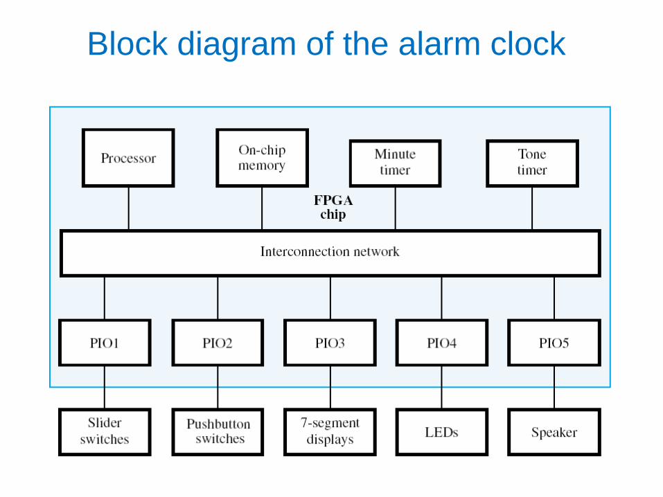
Block diagram of the alarm clock

Parallel I/O Interface - PIO
PIO is a parameterized module that can be used
for both input and output purposes. It can be
configured at design time as:
• an input port
• an output port
• a bidirectional port

Registers in the PIO interface

Interval Timer
• Includes a counter whose contents are decremented
by one in each clock cycle
• It can raise an interrupt request when the contents of
the counter reach zero
• It can be programmed for continuous operation,
where the counter is reset to its starting value each
time its contents are decremented to zero

Registers in the Interval Timer interface

Figure 11.6
Continued on the next slide

Figure 11.6 (continued)
Continued on the next slide

Figure 11.7
Continued on the next slide

Figure11.7 (continued)
Continued on the next slide


Figure 11.7 (continued)
Continued on the next slide

Figure 11.7 (continued)

Figure 11.7 (continued)
Continued on the next slide

Figure 11.7 (continued)
Continued on the next slide

Figure 11.7 (continued)
Continued on the next slide

Figure 11.7 (continued)

SOPC系统

[email protected] 44/94

实验二,基本嵌入式系统-LED,仿真调试

实验二,另一种仿真验证模式,是否可行?
• 将如下代码转成Nios II机器指令,存入RAM
• 编写testbench,分析output端口led的波形

Nios II的特殊控制指令

GUI Elements on the System Generation Tab