spi block user guide v02
TRANSCRIPT

DOCUMENT NUMBERS12SPIV2/D
SPI
Block User Guide
V02.07
Original Release Date: 21 JAN 2000
Motorola, Inc.
Revised: 11 Dec 2002
Motorola reserves the right to make changes without further notice to any products herein to improve reliability, function ordesign. Motorola does not assume any liability arising out of the application or use of any product or circuit described herein;neither does it convey any license under its patent rights nor the rights of others. Motorola products are not designed, intended,or authorized for use as components in systems intended for surgical implant into the body, or other applications intended tosupport or sustain life, or for any other application in which the failure of the Motorola product could create a situation wherepersonal injury or death may occur. Should Buyer purchase or use Motorola products for any such unintended or unauthorizedapplication, Buyer shall indemnify and hold Motorola and its officers, employees, subsidiaries, affiliates, and distributors harmlessagainst all claims, costs, damages, and expenses, and reasonable attorney fees arising out of, directly or indirectly, any claim ofpersonal injury or death associated with such unintended or unauthorized use, even if such claim alleges that Motorola wasnegligent regarding the design or manufacture of the part.
1
SPI Block User Guide — S12SPIV2/D V02.07
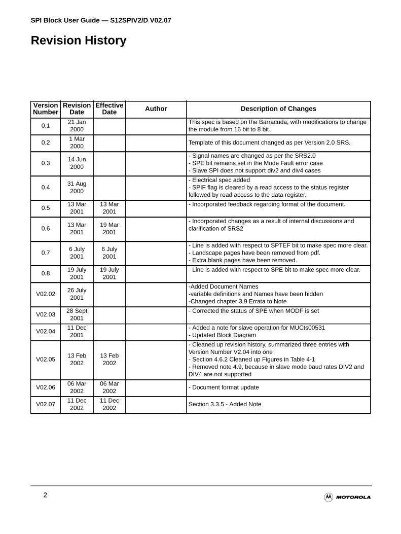
Revision History
VersionNumber
RevisionDate
EffectiveDate Author Description of Changes
0.121 Jan2000
This spec is based on the Barracuda, with modifications to changethe module from 16 bit to 8 bit.
0.21 Mar2000
Template of this document changed as per Version 2.0 SRS.
0.314 Jun2000
- Signal names are changed as per the SRS2.0- SPE bit remains set in the Mode Fault error case- Slave SPI does not support div2 and div4 cases
0.431 Aug2000
- Electrical spec added- SPIF flag is cleared by a read access to the status registerfollowed by read access to the data register.
0.513 Mar2001
13 Mar2001
- Incorporated feedback regarding format of the document.
0.613 Mar2001
19 Mar2001
- Incorporated changes as a result of internal discussions andclarification of SRS2
0.76 July2001
6 July2001
- Line is added with respect to SPTEF bit to make spec more clear.- Landscape pages have been removed from pdf.- Extra blank pages have been removed.
0.819 July2001
19 July2001
- Line is added with respect to SPE bit to make spec more clear.
V02.0226 July2001
-Added Document Names-variable definitions and Names have been hidden-Changed chapter 3.9 Errata to Note
V02.0328 Sept
2001- Corrected the status of SPE when MODF is set
V02.0411 Dec2001
- Added a note for slave operation for MUCts00531- Updated Block Diagram
V02.0513 Feb2002
13 Feb2002
- Cleaned up revision history, summarized three entries withVersion Number V2.04 into one- Section 4.6.2 Cleaned up Figures in Table 4-1- Removed note 4.9, because in slave mode baud rates DIV2 andDIV4 are not supported
V02.0606 Mar2002
06 Mar2002
- Document format update
V02.0711 Dec2002
11 Dec2002
Section 3.3.5 - Added Note
2

SPI Block User Guide — V02.07
Table of Contents
Section 1 Introduction
1.1 Overview. . . . . . . . . . . . . . . . . . . . . . . . . . . . . . . . . . . . . . . . . . . . . . . . . . . . . . . . . . . 9
1.2 Features . . . . . . . . . . . . . . . . . . . . . . . . . . . . . . . . . . . . . . . . . . . . . . . . . . . . . . . . . . . 9
1.3 Modes of Operation . . . . . . . . . . . . . . . . . . . . . . . . . . . . . . . . . . . . . . . . . . . . . . . . . . 9
1.4 Block Diagram . . . . . . . . . . . . . . . . . . . . . . . . . . . . . . . . . . . . . . . . . . . . . . . . . . . . . 10
Section 2 Signal Description
2.1 Overview. . . . . . . . . . . . . . . . . . . . . . . . . . . . . . . . . . . . . . . . . . . . . . . . . . . . . . . . . . 11
2.2 Detailed Signal Descriptions. . . . . . . . . . . . . . . . . . . . . . . . . . . . . . . . . . . . . . . . . . . 11
2.2.1 MOSI . . . . . . . . . . . . . . . . . . . . . . . . . . . . . . . . . . . . . . . . . . . . . . . . . . . . . . . . . . 11
2.2.2 MISO . . . . . . . . . . . . . . . . . . . . . . . . . . . . . . . . . . . . . . . . . . . . . . . . . . . . . . . . . . 11
2.2.3 SS . . . . . . . . . . . . . . . . . . . . . . . . . . . . . . . . . . . . . . . . . . . . . . . . . . . . . . . . . . . . 11
2.2.4 SCK . . . . . . . . . . . . . . . . . . . . . . . . . . . . . . . . . . . . . . . . . . . . . . . . . . . . . . . . . . . 11
Section 3 Memory Map and Registers
3.1 Overview. . . . . . . . . . . . . . . . . . . . . . . . . . . . . . . . . . . . . . . . . . . . . . . . . . . . . . . . . . 13
3.2 Module Memory Map . . . . . . . . . . . . . . . . . . . . . . . . . . . . . . . . . . . . . . . . . . . . . . . . 13
3.3 Register Descriptions . . . . . . . . . . . . . . . . . . . . . . . . . . . . . . . . . . . . . . . . . . . . . . . . 13
3.3.1 SPI Control Register 1 . . . . . . . . . . . . . . . . . . . . . . . . . . . . . . . . . . . . . . . . . . . . . 14
3.3.2 SPI Control Register 2 . . . . . . . . . . . . . . . . . . . . . . . . . . . . . . . . . . . . . . . . . . . . . 15
3.3.3 SPI Baud Rate Register . . . . . . . . . . . . . . . . . . . . . . . . . . . . . . . . . . . . . . . . . . . . 16
3.3.4 SPI Status Register . . . . . . . . . . . . . . . . . . . . . . . . . . . . . . . . . . . . . . . . . . . . . . . 19
3.3.5 SPI Data Register . . . . . . . . . . . . . . . . . . . . . . . . . . . . . . . . . . . . . . . . . . . . . . . . 20
Section 4 Functional Description
4.1 General. . . . . . . . . . . . . . . . . . . . . . . . . . . . . . . . . . . . . . . . . . . . . . . . . . . . . . . . . . . 21
4.2 Master Mode. . . . . . . . . . . . . . . . . . . . . . . . . . . . . . . . . . . . . . . . . . . . . . . . . . . . . . . 21
4.3 Slave Mode. . . . . . . . . . . . . . . . . . . . . . . . . . . . . . . . . . . . . . . . . . . . . . . . . . . . . . . . 22
4.4 Transmission Formats . . . . . . . . . . . . . . . . . . . . . . . . . . . . . . . . . . . . . . . . . . . . . . . 23
4.4.1 Clock Phase and Polarity Controls. . . . . . . . . . . . . . . . . . . . . . . . . . . . . . . . . . . . 23
4.4.2 CPHA = 0 Transfer Format . . . . . . . . . . . . . . . . . . . . . . . . . . . . . . . . . . . . . . . . . 24
4.4.3 CPHA = 1 Transfer Format . . . . . . . . . . . . . . . . . . . . . . . . . . . . . . . . . . . . . . . . . 25
4.5 SPI Baud Rate Generation . . . . . . . . . . . . . . . . . . . . . . . . . . . . . . . . . . . . . . . . . . . . 27
3

SPI Block User Guide — V02.07
4.6 Special Features. . . . . . . . . . . . . . . . . . . . . . . . . . . . . . . . . . . . . . . . . . . . . . . . . . . . 27
4.6.1 SS Output. . . . . . . . . . . . . . . . . . . . . . . . . . . . . . . . . . . . . . . . . . . . . . . . . . . . . . . 27
4.6.2 Bidirectional Mode (MOMI or SISO). . . . . . . . . . . . . . . . . . . . . . . . . . . . . . . . . . . 28
4.7 Error Conditions . . . . . . . . . . . . . . . . . . . . . . . . . . . . . . . . . . . . . . . . . . . . . . . . . . . . 28
4.7.1 Mode Fault Error . . . . . . . . . . . . . . . . . . . . . . . . . . . . . . . . . . . . . . . . . . . . . . . . . 29
4.8 Low Power Mode Options . . . . . . . . . . . . . . . . . . . . . . . . . . . . . . . . . . . . . . . . . . . . 29
4.8.1 SPI in Run Mode . . . . . . . . . . . . . . . . . . . . . . . . . . . . . . . . . . . . . . . . . . . . . . . . . 29
4.8.2 SPI in Wait Mode . . . . . . . . . . . . . . . . . . . . . . . . . . . . . . . . . . . . . . . . . . . . . . . . . 29
4.8.3 SPI in Stop Mode . . . . . . . . . . . . . . . . . . . . . . . . . . . . . . . . . . . . . . . . . . . . . . . . . 30
Section 5 Reset
5.1 General. . . . . . . . . . . . . . . . . . . . . . . . . . . . . . . . . . . . . . . . . . . . . . . . . . . . . . . . . . . 31
Section 6 Interrupts
6.1 Interrupt Operation . . . . . . . . . . . . . . . . . . . . . . . . . . . . . . . . . . . . . . . . . . . . . . . . . . 33
6.1.1 MODF. . . . . . . . . . . . . . . . . . . . . . . . . . . . . . . . . . . . . . . . . . . . . . . . . . . . . . . . . . 33
6.1.2 SPIF . . . . . . . . . . . . . . . . . . . . . . . . . . . . . . . . . . . . . . . . . . . . . . . . . . . . . . . . . . . 33
6.1.3 SPTEF . . . . . . . . . . . . . . . . . . . . . . . . . . . . . . . . . . . . . . . . . . . . . . . . . . . . . . . . . 33
4

SPI Block User Guide — V02.07
List of Figures
Figure 1-1 SPI Block Diagram. . . . . . . . . . . . . . . . . . . . . . . . . . . . . . . . . . . . . . . . . . . . . 10
Figure 3-2 SPI Control Register 1 (SPICR1). . . . . . . . . . . . . . . . . . . . . . . . . . . . . . . . . . 14
Figure 3-3 SPI Control Register 2 (SPICR2). . . . . . . . . . . . . . . . . . . . . . . . . . . . . . . . . . 15
Figure 3-4 SPI Baud Rate Register (SPIBR) . . . . . . . . . . . . . . . . . . . . . . . . . . . . . . . . . 16
Figure 3-5 SPI Status Register (SPISR) . . . . . . . . . . . . . . . . . . . . . . . . . . . . . . . . . . . . . 19
Figure 3-6 SPI Data Register (SPIDR) . . . . . . . . . . . . . . . . . . . . . . . . . . . . . . . . . . . . . . 20
Figure 4-1 Master/Slave Transfer Block Diagram. . . . . . . . . . . . . . . . . . . . . . . . . . . . . . 23
Figure 4-2 SPI Clock Format 0 (CPHA = 0) . . . . . . . . . . . . . . . . . . . . . . . . . . . . . . . . . . 25
Figure 4-3 SPI Clock Format 1 (CPHA = 1) . . . . . . . . . . . . . . . . . . . . . . . . . . . . . . . . . . 26
Figure 4-4 Baud Rate Divisor Equation. . . . . . . . . . . . . . . . . . . . . . . . . . . . . . . . . . . . . . 27
5

SPI Block User Guide — V02.07
6

SPI Block User Guide — V02.07
List of Tables
Table 3-1 Module Memory Map . . . . . . . . . . . . . . . . . . . . . . . . . . . . . . . . . . . . . . . . . . . . 13
Table 3-2 SS Input / Output Selection . . . . . . . . . . . . . . . . . . . . . . . . . . . . . . . . . . . . . . . 15
Table 3-3 Bidirectional Pin Configurations. . . . . . . . . . . . . . . . . . . . . . . . . . . . . . . . . . . . 16
Table 3-4 SPI Baud Rate Selection . . . . . . . . . . . . . . . . . . . . . . . . . . . . . . . . . . . . . . . . 17
Table 4-1 Normal Mode and Bidirectional Mode . . . . . . . . . . . . . . . . . . . . . . . . . . . . . . . 28
7

SPI Block User Guide — V02.07
8

SPI Block User Guide — V02.07
heral
ternaln canwait
lonized
s note
n
Section 1 Introduction
1.1 Overview
The SPI module allows a duplex, synchronous, serial communication between the MCU and peripdevices. Software can poll the SPI status flags or the SPI operation can be interrupt driven.
1.2 Features
The SPI includes these distinctive features:
• Master mode and slave mode
• Bi-directional mode
• Slave select output
• Mode fault error flag with CPU interrupt capability
• Double-buffered operation
• Serial clock with programmable polarity and phase
• Control of SPI operation during wait mode
1.3 Modes of Operation
The SPI functions in three modes, run, wait, and stop.
• Run Mode
This is the basic mode of operation.
• Wait Mode
SPI operation in wait mode is a configurable low power mode. Depending on the state of inbits, the SPI can operate normally when the CPU is in wait mode or the SPI clock generatiobe turned off and the SPI module enters a power conservation state during wait mode. Duringmode, any master transmission in progress stops if the SPISWAI bit is set in the SPI controregister2. Reception and transmission of a byte as slave continues so that the slave is synchrto the master.
• Stop Mode
The SPI is inactive in stop mode for reduced power consumption. The STOP instruction doeaffect or depend on SPI register states. Again, reception and transmission of a byte as slavcontinues to stay synchronized with the master.
This is a high level description only, detailed descriptions of operating modes are contained in sectio4.8Low Power Mode Options .
9

SPI Block User Guide — V02.07
1.4 Block Diagram
Figure 1-1 is a general block diagram of the SPI.
Figure 1-1 SPI Block Diagram
PINCONTROL
LOGIC
8-BIT SHIFT REGISTER
CLOCKLOGIC
SPI CONTROL
SPI STATUS REGISTER
SPI DATA REGISTER
DIVIDER
SELECT
SPI BAUD RATE REGISTER
2 4 8 16 32 64 128 256
SPI
INTE
RRU
PT
SM
M
S
M
S
REQ
UES
T
SPI CONTROL REGISTER 1
BAUD RATE GENERATOR
MISO
MOSI
SPI CONTROL REGISTER 2
SS
SCK
BUS CLOCK
MO
DF
SPIF
SPTE
F
SPPR
2
SPPR
1
SPR
1
SPR
0
SPPR
0
SPR
2
MST
R
CPH
A
CPO
L
LSBF
EBIDIROESPC0
BAUD CLOCK
IPBUS
MUXED CLOCK
10

SPI Block User Guide — V02.07
11
Section 2 Signal Description
2.1 Overview
This section lists the name and description of all ports including inputs and outputs that do, or may, connectoff chip. The SPI module has a total of 4 external pins.
2.2 Detailed Signal Descriptions
2.2.1 MOSI
This pin is used to transmit data out of the SPI module when it is configured as a Master and receive datawhen it is configured as slave.
2.2.2 MISO
This pin is used to transmit data out of the SPI module when it is configured as a Slave and receive datawhen it is configured as Master.
2.2.3 SS
This pin is used to output the select signal from the SPI module to another peripheral with which a datatransfer is to take place.
2.2.4 SCK
This pin is used to output the clock with respect to which the SPI transfers data or receive clock in case ofSlave.

SPI Block User Guide — V02.07
12

SPI Block User Guide — V02.07
r.
mess offsetd bits
registerter
Section 3 Memory Map and Registers
3.1 Overview
This section provides a detailed description of all memory and registers accessible to the end use
3.2 Module Memory Map
The memory map for the SPI is given below inTable 3-1 . The address listed for each register is the suof a base address and an address offset. The base address is defined at the SoC level and the addris defined at the module level. Reads from the reserved bits return zeros and writes to the reservehave no effect.
3.3 Register Descriptions
This section consists of register descriptions in address order. Each description includes a standarddiagram with an associated figure number. Details of register bit and field function follow the regisdiagrams, in bit order.
Table 3-1 Module Memory Map
Address Use Access$___0 SPI Control Register 1 (SPICR1) Read / Write
$___1 SPI Control Register 2 (SPICR2) Read / Write 1
NOTES:1. Certain bits are non-writable.
$___2 SPI Baud Rate Register (SPIBR) Read / Write 1
$___3 SPI Status Register (SPISR) Read 2
2. Writes to this register are ignored.
$___4 Reserved — 2 3
3. Reading from this register returns all zeros.
$___5 SPI Data Register (SPIDR) Read / Write
$___6 Reserved — 2 3
$___7 Reserved — 2 3
13

SPI Block User Guide — V02.07
e SPI
3.3.1 SPI Control Register 1
Figure 3-2 SPI Control Register 1 (SPICR1)
Read: anytimeWrite: anytime
SPIE — SPI Interrupt Enable Bit
This bit enables SPI interrupts each time the SPIF or MODF status flag is set.1 = SPI interrupts enabled.0 = SPI interrupts disabled.
SPE — SPI System Enable Bit
This bit enables the SPI system and dedicates the SPI port pins to SPI system functions.1 = SPI port pins are dedicated to SPI functions.0 = SPI disabled (lower power consumption).
SPTIE — SPI Transmit Interrupt Enable
This bit enables SPI interrupt generated each time the SPTEF flag is set.1 = SPTEF interrupt enabled.0 = SPTEF interrupt disabled.
MSTR — SPI Master/Slave Mode Select Bit1 = Master mode0 = Slave mode
CPOL — SPI Clock Polarity Bit
This bit selects an inverted or non-inverted SPI clock. To transmit data between SPI modules, thmodules must have identical CPOL values.
1 = Active-low clocks selected; SCK idles high0 = Active-high clocks selected; SCK idles low
CPHA — SPI Clock Phase Bit
This bit is used to shift the SCK serial clock.1 = The first SCK edge is issued at the beginning of the 8-cycle transfer operation0 = The first SCK edge is issued one-half cycle into the 8-cycle transfer operation
Register Address: $___0
Bit 7 6 5 4 3 2 1 Bit 0R
SPIE SPE SPTIE MSTR CPOL CPHA SSOE LSBFEW
Reset: 0 0 0 0 0 1 0 0
14

SPI Block User Guide — V02.07
e data
oes
SSOE — Slave Select Output Enable
TheSS output feature is enabled only in the master mode by asserting the SSOE as shown inTable3-2.
LSBFE — SPI LSB-First Enable
This bit does not affect the position of the msb and lsb in the data register. Reads and writes of thregister always have the msb in bit 7.
1 = Data is transferred least significant bit first.0 = Data is transferred most significant bit first.
3.3.2 SPI Control Register 2
Figure 3-3 SPI Control Register 2 (SPICR2)
Read: anytimeWrite: anytime; writes to the reserved bits have no effect
MODFEN — Mode Fault Enable Bit
This bit when set allows the MODF flag to be set. If the MODF flag is set, clearing the MODFEN dnot clear the MODF flag. If the SPI is enabled as master and the MODFEN bit is low, then theSS pinis not used by the SPI.
When the SPI is enabled as a slave, theSS is available only as an input regardless of the value ofMODFEN.
1 = Enable setting the MODF error0 = Disable the MODF error
Table 3-2 SS Input / Output Selection
MODFEN SSOE Master Mode Slave Mode
0 0 SS not used by SPI SS input
0 1 SS not used by SPI SS input
1 0 SS input with MODF feature SS input
1 1 SS output SS input
Register Address: $___1
Bit 7 6 5 4 3 2 1 Bit 0R 0 0 0
MODFEN BIDIROE0
SPISWAI SPC0W
Reset: 0 0 0 0 0 0 0 0
= Reserved
15

SPI Block User Guide — V02.07
BIDIROE — Output enable in the Bidirectional mode of operation
This bit along with the MSTR bit of SPCR1 is used to enable the output buffer when the SPI isconfigured in bidirectional mode.
1 = Output buffer enabled0 = Output buffer disabled
SPISWAI — SPI Stop in Wait Mode Bit
This bit is used for power conservation while in wait mode.1 = Stop SPI clock generation when in wait mode0 = SPI clock operates normally in wait mode
SPC0 — Serial Pin Control Bit 0
With the MSTR control bit, this bit enables bidirectional pin configurations as shown inTable 3-3 .
3.3.3 SPI Baud Rate Register
Figure 3-4 SPI Baud Rate Register (SPIBR)
Read: anytimeWrite: anytime; writes to the reserved bits have no effect
NOTE: Writing to this register during data transfers may cause spurious results.
Table 3-3 Bidirectional Pin Configurations
Pin Mode SPC0 MSTR MISO 1
NOTES:1. Slave output is enabled if BIDIROE bit = 1, SS = 0, and MSTR = 0 (C)
MOSI 2
2. Master output is enabled if BIDIROE bit = 1 and MSTR = 1 (D)
SCK 3
3. SCK output is enabled if MSTR = 1 (B, D)
SS 4
4. SS output is enabled if MODFEN bit = 1, SSOE = 1, and MSTR = 1 (B, D).
ANormal 0
0 Slave Out Slave In SCK in SS in
B 1 Master In Master Out SCK out SS I/O
CBidirectional 1
0 Slave I/O — SCK in SS In
D 1 — Master I/O SCK out SS I/O
Register Address: $___2
Bit 7 6 5 4 3 2 1 Bit 0R 0
SPPR2 SPPR1 SPPR00
SPR2 SPR1 SPR0W
Reset: 0 0 0 0 0 0 0 0
= Reserved
16

SPI Block User Guide — V02.07
SPPR2–SPPR0 — SPI Baud Rate Preselection Bits
SPR2–SPR0 — SPI Baud Rate Selection Bits
These bits specify the SPI baud rates as shown in the table below
The baud rate divisor equation is as follows
Baud Rate = Bus clock / BaudRateDivisor
Table 3-4 SPI Baud Rate Selection
SPPR2 SPPR1 SPPR0 SPR2 SPR1 SPR0 SPI ModuleClock Divisor
0 0 0 0 0 0 2
0 0 0 0 0 1 4
0 0 0 0 1 0 8
0 0 0 0 1 1 16
0 0 0 1 0 0 32
0 0 0 1 0 1 64
0 0 0 1 1 0 128
0 0 0 1 1 1 256
0 0 1 0 0 0 4
0 0 1 0 0 1 8
0 0 1 0 1 0 16
0 0 1 0 1 1 32
0 0 1 1 0 0 64
0 0 1 1 0 1 128
0 0 1 1 1 0 256
0 0 1 1 1 1 512
0 1 0 0 0 0 6
0 1 0 0 0 1 12
0 1 0 0 1 0 24
0 1 0 0 1 1 48
0 1 0 1 0 0 96
0 1 0 1 0 1 192
0 1 0 1 1 0 384
0 1 0 1 1 1 768
0 1 1 0 0 0 8
0 1 1 0 0 1 16
0 1 1 0 1 0 32
0 1 1 0 1 1 64
0 1 1 1 0 0 128
0 1 1 1 0 1 256
BaudRateDivisor SPPR 1+( ) 2• SPR 1+( )=
17

SPI Block User Guide — V02.07
NOTE: DIV2 and DIV4 are not supported in slave mode of SPI.
0 1 1 1 1 0 512
0 1 1 1 1 1 1024
1 0 0 0 0 0 10
1 0 0 0 0 1 20
1 0 0 0 1 0 40
1 0 0 0 1 1 80
1 0 0 1 0 0 160
1 0 0 1 0 1 320
1 0 0 1 1 0 640
1 0 0 1 1 1 1280
1 0 1 0 0 0 12
1 0 1 0 0 1 24
1 0 1 0 1 0 48
1 0 1 0 1 1 96
1 0 1 1 0 0 192
1 0 1 1 0 1 384
1 0 1 1 1 0 768
1 0 1 1 1 1 1536
1 1 0 0 0 0 14
1 1 0 0 0 1 28
1 1 0 0 1 0 56
1 1 0 0 1 1 112
1 1 0 1 0 0 224
1 1 0 1 0 1 448
1 1 0 1 1 0 896
1 1 0 1 1 1 1792
1 1 1 0 0 0 16
1 1 1 0 0 1 32
1 1 1 0 1 0 64
1 1 1 0 1 1 128
1 1 1 1 0 0 256
1 1 1 1 0 1 512
1 1 1 1 1 0 1024
1 1 1 1 1 1 2048
Table 3-4 SPI Baud Rate Selection
SPPR2 SPPR1 SPPR0 SPR2 SPR1 SPR0 SPI ModuleClock Divisor
18

SPI Block User Guide — V02.07
gister
TEF
anly setI (noR isconde inanditingfter.
aredPIer to
3.3.4 SPI Status Register
Figure 3-5 SPI Status Register (SPISR)
Read: anytimeWrite: has no effect
SPIF — SPIF Interrupt Flag
This bit is set after the eighth SCK cycle in a data transfer and is cleared by reading the SPISR re(with SPIF set) followed by a read access to the SPI data register.
1 = New data Copied to SPIDR0 = Transfer not yet complete
SPTEF — SPI Transmit Empty Interrupt Flag
This bit is set when there is room in the transmit data buffer. It is cleared by reading SPISR with SPset, followed by writing a data value to the transmit buffer at SPIDR.SPISR must be read withSPTEF=1 before writing data to SPIDR or the SPIDR write will be ignored. SPTEF generates SPTEF CPU interrupt request if the SPTIE bit in the SPICR1 is also set.SPTEF is automaticalwhen a data byte transfers from the transmit buffer into the transmit shift register. For an idle SPdata in the transmit buffer or the shift register and no transfer in progress), data written to SPIDtransferred to the shifter almost immediately so SPTEF is set within two bus cycles allowing a se8-bit data value to be queued into the transmit buffer. After completion of the transfer of the valuthe shift register, the queued value from the transmit buffer will automatically move to the shifterSPTEF will be set to indicate there is room for new data in the transmit buffer. If no new data is wain the transmit buffer, SPTEF simply remains set and no data moves from the buffer to the shi
1 = SPI Data register empty0 = SPI Data register not empty
NOTE: Do not write to the SPI data register unless the SPTEF bit is high. Any such writeto the SPI Data Register before reading SPTEF=1 is effectively ignored
MODF — Mode Fault Flag
This bit is set if theSS input becomes low while the SPI is configured as a master. The flag is cleautomatically by a read of the SPI status register (with MODF set) followed by a write to the Scontrol register 1. The MODF flag is set only if the MODFEN bit of SPICR2 register is set. RefMODFEN bit description in3.3.2 SPI Control Register 2 .
1 = Mode fault has occurred.0 = Mode fault has not occurred.
Register Address: $___3
Bit 7 6 5 4 3 2 1 Bit 0R SPIF 0 SPTEF MODF 0 0 0 0W
Reset: 0 0 1 0 0 0 0 0
= Reserved
19

SPI Block User Guide — V02.07
llowste ismpty
sfer. Ifthe data
3.3.5 SPI Data Register
Figure 3-6 SPI Data Register (SPIDR)
Read: anytime; normally read only after SPIF is setWrite: anytime; see SPTEF
The SPI Data register is both the input and output register for SPI data. A write to this register aa data byte to be queued and transmitted. For a SPI configured as a master, a queued data bytransmitted immediately after the previous transmission has completed. The SPI Transmitter eflag in SPISR indicates when the SPI data register is ready to accept new data.
NOTE: Do not write to the SPI data register unless the SPTEF bit is high.
Reading the data can occur anytime from after the SPIF is set to before the end of the next tranthe SPIF is not serviced by the end of the successive transfers, those data bytes are lost and within the SPIDR retains the first byte until SPIF is serviced.
NOTE: After reset the content of the SPI Shift Register is undefined until a data byte isstored into SPIDR.
Register Address: $___5
Bit 7 6 5 4 3 2 1 Bit 0R
Bit 7 6 5 4 3 2 2 Bit 0W
Reset: 0 0 0 0 0 0 0 0
20

SPI Block User Guide — V02.07
heral
is set,
and theister.y themaster
register
plete.d from
acts asegister
er 1cts at
1 is set,
ter isSI pin
SPPR0ine the
Section 4 Functional Description
4.1 General
The SPI module allows a duplex, synchronous, serial communication between the MCU and peripdevices. Software can poll the SPI status flags or SPI operation can be interrupt driven.
The SPI system is enabled by setting the SPI enable (SPE) bit in SPI control register 1. While SPEthe four associated SPI port pins are dedicated to the SPI function as:
• Slave select (SS)
• Serial clock (SCK)
• Master out/slave in (MOSI)
• Master in/slave out (MISO)
The main element of the SPI system is the SPI data register. The 8-bit data register in the master8-bit data register in the slave are linked by the MOSI and MISO pins to form a distributed 16-bit regWhen a data transfer operation is performed, this 16-bit register is serially shifted eight bit positions bSCK clock from the master; data is exchanged between the master and the slave. Data written to theSPI data register becomes the output data for the slave, and data read from the master SPI data after a transfer operation is the input data from the slave.
A write to the SPI data register puts data into the transmit buffer if the previous transmission was comWhen a transfer is complete, received data is moved into a receive data register. Data may be reathis double-buffered system any time before the next transfer is complete. This 8-bit data registerthe SPI receive data register for reads and as the SPI transmit data register for writes. A single SPI raddress is used for reading data from the read data buffer and for writing data to the shifter.
The clock phase control bit (CPHA) and a clock polarity control bit (CPOL) in the SPI control registselect one of four possible clock formats to be used by the SPI system. The CPOL bit simply selenon-inverted or inverted clock. The CPHA bit is used to accommodate two fundamentally differenprotocols by shifting the clock by a half cycle or by not shifting the clock (see4.4 TransmissionFormats).
The SPI can be configured to operate as a master or as a slave. When MSTR in SPI control registerthe master mode is selected; when the MSTR bit is clear, the slave mode is selected.
4.2 Master Mode
The SPI operates in master mode when the MSTR bit is set. Only a master SPI module can initiatransmissions. A transmission begins by writing to the master SPI data register. If the shift registeempty, the byte immediately transfers to the shift register. The byte begins shifting out on the MOunder the control of the serial clock.
The SPR2, SPR1, and SPR0 baud rate selection bits in conjunction with the SPPR2, SPPR1, andbaud rate preselection bits in the SPI baud rate register control the baud rate generator and determ
21

SPI Block User Guide — V02.07
te
O) is
ster
. If themore
SPIpinsmodeDF
delay,clock
, SCKurs,
, theghpin.he
g SPI
ible forceive
ata atfrom the
speed of the shift register. The SCK pin is the SPI clock output. Through the SCK pin, the baud ragenerator of the master controls the shift register of the slave peripheral.
In master mode, the function of the serial data output pin (MOSI) and the serial data input pin (MISdetermined by the SPC0 and MSTR control bits.
TheSS pin is normally an input which should remain in the inactive high state. However, in the mamode, if both MODFEN bit and SSOE bit are set, then theSS pin is the slave select output.
TheSS output becomes low during each transmission and is high when the SPI is in the idling stateSS input becomes low while the SPI is configured as a master, it indicates a mode fault error wherethan one master may be trying to drive the MOSI and SCK lines simultaneously. In this case, the immediately clears the output buffer enables associated with the MISO, MOSI (or MOMI), and SCKso that these pins become inputs. This mode fault error also clears the MSTR control bit and sets thefault (MODF) flag in the SPI status register. If the SPI interrupt enable bit (SPIE) is set when the MObit gets set, then an SPI interrupt sequence is also requested
When a write to the SPI data register in the master occurs, there is a half SCK-cycle delay. After theSCK is started within the master. The rest of the transfer operation differs slightly, depending on theformat specified by the SPI clock phase bit, CPHA, in SPI control register 1 (see4.4 TransmissionFormats).
4.3 Slave Mode
The SPI operates in slave mode when the MSTR bit in SPI control register1 is clear. In slave modeis the SPI clock input from the master, andSS is the slave select input. Before a data transmission occtheSS pin of the slave SPI must be at logic 0.SS must remain low until the transmission is complete.
In slave mode, the function of the serial data output pin (MISO) and serial data input pin (MOSI) isdetermined by the SPC0 bit in SPI control register 2 and the MSTR control bit. While in slave modeSS input controls the serial data output pin; ifSS is high (not selected), the serial data output pin is hiimpedance, and, ifSS is low the first bit in the SPI data register is driven out of the serial data outputAlso, if the slave is not selected (SS is high), then the SCK input is ignored and no internal shifting of tSPI shift register takes place.
Although the SPI is capable of duplex operation, some SPI peripherals are capable of only receivindata in a slave mode. For these simpler devices, there is no serial data out pin.
NOTE: When peripherals with duplex capability are used, take care not to simultaneouslyenable two receivers whose serial outputs drive the same system slave’s serial dataoutput line.
As long as no more than one slave device drives the system slave’s serial data output line, it is possseveral slaves to receive the same transmission from a master, although the master would not rereturn information from all of the receiving slaves.
If the CPHA bit in SPI control register 1 is clear, odd numbered edges on the SCK input cause the dthe serial data input pin to be latched. Even numbered edges cause the value previously latched serial data input pin to shift into the LSB of the SPI shifter.
22

SPI Block User Guide — V02.07
put pinto shift
PHAdatasferred is set.
lly)two
es thatselect
hase
t on
.
If the CPHA bit is set, even numbered edges on the SCK input cause the data at the serial data into be latched. Odd numbered edges cause the value previously latched from the serial data input pininto the LSB of the SPI shifter.
NOTE: In slave mode, the control bits CPHA and CPOL of the SPI should be configuredonly when SPI is disabled else it may lead to incorrect data transfer. Care must betaken to avoid driver collisions in SPI disabled state, because SPI port pins are thennot under the control of the SPI. For recommended actions refer to the Device UserGuide, SPI section.
When CPHA is set, the first edge is used to get the first data bit onto the serial data output pin. When Cis clear and theSS input is low (slave selected), the first bit of the SPI data is driven out of the serialoutput pin. After the eighth shift, the transfer is considered complete and the received data is traninto the SPI data register. To indicate transfer is complete, the SPIF flag in the SPI status register
4.4 Transmission Formats
During an SPI transmission, data is transmitted (shifted out serially) and received (shifted in seriasimultaneously. The serial clock (SCK) synchronizes shifting and sampling of the information on theserial data lines. A slave select line allows selection of an individual slave SPI device; slave devicare not selected do not interfere with SPI bus activities. Optionally, on a master SPI device, the slaveline can be used to indicate multiple-master bus contention.
Figure 4-1 Master/Slave Transfer Block Diagram
4.4.1 Clock Phase and Polarity Controls
Using two bits in the SPI control register1, software selects one of four combinations of serial clock pand polarity.
The CPOL clock polarity control bit specifies an active high or low clock and has no significant effecthe transmission format.
The CPHA clock phase control bit selects one of two fundamentally different transmission formats
SHIFT REGISTER
SHIFT REGISTER
BAUD RATEGENERATOR
MASTER SPI SLAVE SPI
VDD
MOSI MOSI
MISO MISO
SCK SCK
SS SS
23

SPI Block User Guide — V02.07
ver device
st datae data
f cycleA bit.
t edgeoccurs,
put pine SCK
r and
ter and
OL SCK,
l is the
Clock phase and polarity should be identical for the master SPI device and the communicating sladevice. In some cases, the phase and polarity are changed between transmissions to allow a masteto communicate with peripheral slaves having different requirements.
NOTE: It is recommended that software writes to the SPI control register to change CPHA,CPOL or MSTR bits only in the idle state of the SPI. If these bits are changed duringthe transmission, data transmission gets corrupted.
4.4.2 CPHA = 0 Transfer Format
The first edge on the SCK line is used to clock the first data bit of slave into the master and the firbit of master into the slave. In some peripherals, the first bit of the slave's data is available at the slavout pin as soon as the slave is selected. In this format, the first SCK edge is not issued until a halinto the 8-cycle transfer operation. The first edge of SCK is delayed a half cycle by clearing the CPH
The SCK output from the master remains in the inactive state for a half SCK period before the firsappears. A half SCK cycle later, the second edge appears on the SCK line. When this second edgethe value previously latched from the serial data input pin is shifted into the LSB of the shifter.
After this second edge, the next bit of the SPI master data is transmitted out of the serial data outof the master to the serial input pin on the slave. This process continues for a total of 16 edges on thline, with data being latched on odd numbered edges and shifted on even numbered edges.
Data reception is double buffered. Data is shifted serially into the SPI shift register during the transfeis transferred to the parallel SPI data register after the last bit is shifted in.
After the 16th (last) SCK edge:
• Data that was previously in the master SPI data register should now be in the slave data registhe data that was in the slave data register should be in the master.
• The SPIF flag in the SPI status register is set indicating that the transfer is complete.
Figure 4-2 is a timing diagram of an SPI transfer where CPHA = 0. SCK waveforms are shown for CP= 0 and CPOL = 1. The diagram may be interpreted as a master or slave timing diagram since theMISO, and MOSI pins are connected directly between the master and the slave. The MISO signaoutput from the slave and the MOSI signal is the output from the master. TheSS pin of the master mustbe either high or reconfigured as a general-purpose output not affecting the SPI.
24

SPI Block User Guide — V02.07
essive
ead the
ut pin;g the
firstaster.
h the
Figure 4-2 SPI Clock Format 0 (CPHA = 0)
TheSS line should be deasserted at least for minimum idle time (half SCK cycle) between the succtransfers (SS should not be tied low all the times in this mode). IfSS is not deasserted between thesuccessive transmission then the new byte written to the data register would not be transmitted, instlast received byte would be transmitted.
4.4.3 CPHA = 1 Transfer Format
Some peripherals require the first SCK edge before the first data bit becomes available at the data othe second edge clocks data into the system. In this format, the first SCK edge is issued by settinCPHA bit at the beginning of the 8-cycle transfer operation.
The first edge of SCK occurs immediately after the half SCK clock cycle synchronization delay. Thisedge commands the slave to transfer its most significant data bit to the serial data input pin of the m
A half SCK cycle later, the second edge appears on the SCK pin. This is the latching edge for botmaster and slave.
tL
Begin End
SCK (CPOL = 0)
SAMPLE I
CHANGE O
SEL SS (O)
Transfer
SCK (CPOL = 1)
MSB first (LSBFE = 0): LSB first (LSBFE = 1):
MSBLSB
LSBMSB
Bit 5Bit 2
Bit 6Bit 1
Bit 4Bit 3
Bit 3Bit 4
Bit 2Bit 5
Bit 1Bit 6
CHANGE O
SEL SS (I)
MOSI pin
MISO pin
Master only
MOSI/MISO
tT
If ne
xt tr
ansf
er b
egin
s he
re
for tT, tl, tLMinimum 1/2 SCK
tI tL
tL = Minimum leading time before the first SCK edgetT = Minimum trailing time after the last SCK edgetI = Minimum idling time between transfers (minimum SS high time)tL, tT, and tI are guaranteed for the master mode and required for the slave mode.
25

SPI Block User Guide — V02.07
to theutput
bered
r and
slave,
er orer andaster.
When the third edge occurs, the value previously latched from the serial data input pin is shifted inLSB of the SPI shifter. After this edge, the next bit of the master data is coupled out of the serial data opin of the master to the serial input pins on the slave.
This process continues for a total of 16 edges on the SCK line with data being latched on even numedges and shifting taking place on odd numbered edges.
Data reception is double buffered; data is serially shifted into the SPI shift register during the transfeis transferred to the parallel SPI data register after the last bit is shifted in.
After the 16th SCK edge:
• Data that was previously in the SPI data register of the master is now in the data register of theand data that was in the data register of the slave is in the master.
• The SPIF flag bit in SPISR is set indicating that the transfer is complete.
Figure 4-3 shows two clocking variations for CPHA = 1. The diagram may be interpreted as a mastslave timing diagram since the SCK, MISO, and MOSI pins are connected directly between the mastthe slave. The MISO signal is the output from the slave, and the MOSI signal is the output from the mTheSS line is the slave select input to the slave. TheSS pin of the master must be either high orreconfigured as a general-purpose output not affecting the SPI.
Figure 4-3 SPI Clock Format 1 (CPHA = 1)
tL tT
for tT, tl, tLMinimum 1/2 SCK
tI tL
If ne
xt tr
ansf
er b
egin
s he
re
Begin End
SCK (CPOL = 0)
SAMPLE I
CHANGE O
SEL SS (O)
Transfer
SCK (CPOL = 1)
MSB first (LSBFE = 0): LSB first (LSBFE = 1):
MSBLSB
LSBMSB
Bit 5Bit 2
Bit 6Bit 1
Bit 4Bit 3
Bit 3Bit 4
Bit 2Bit 5
Bit 1Bit 6
CHANGE O
SEL SS (I)
MOSI pin
MISO pin
Master only
MOSI/MISO
tL = Minimum leading time before the first SCK edgetT = Minimum trailing time after the last SCK edgetI = Minimum idling time between transfers (minimum SS high time)tL, tT, and tI are guaranteed for the master mode and required for the slave mode.
26

SPI Block User Guide — V02.07
ormatO data
et aftersfer is
SPPR2,sults in
ivisor
ction divisor
Whenck to
tc.
taking
es
nd
TheSS line can remain active low between successive transfers (can be tied low at all times). This fis sometimes preferred in systems having a single fixed master and a single slave that drive the MISline.
The SPI interrupt request flag (SPIF) is common to both the master and slave modes. SPIF gets sthe last SCK edge in a data transfer operation to indicate that the transfer is complete though tranactually complete half SCK cycle later.
4.5 SPI Baud Rate Generation
Baud rate generation consists of a series of divider stages. Six bits in the SPI baud rate register (SPPR1, SPPR0, SPR2, SPR1, and SPR0) determine the divisor to the SPI module clock which rethe SPI baud rate.
The SPI clock rate is determined by the product of the value in the baud rate preselection bits(SPPR2–SPPR0) and the value in the baud rate selection bits (SPR2–SPR0). The module clock dequation is shown inFigure 4-4 .
When all bits are clear (the default condition), the SPI module clock is divided by 2. When the selebits (SPR2–SPR0) are 001 and the preselection bits (SPPR2–SPPR0) are 000, the module clockbecomes 4. When the selection bits are 010, the module clock divisor becomes 8 etc.
When the preselection bits are 001, the divisor determined by the selection bits is multiplied by 2.the preselection bits are 010, the divisor is multiplied by 3, etc. The two sets of selects allows the clobe divided by a non-power of two to achieve other baud rates such as divide by 6, divide by 10, e
The baud rate generator is activated only when the SPI is in the master mode and a serial transfer isplace. In the other cases, the divider is disabled to decrease IDD current.
Figure 4-4 Baud Rate Divisor Equation
4.6 Special Features
4.6.1 SS Output
TheSS output feature automatically drives theSS pin low during transmission to select external devicand drives it high during idle to deselect external devices. WhenSS output is selected, theSS output pinis connected to theSS input pin of the external device.
TheSS output is available only in master mode during normal SPI operation by asserting SSOE aMODFEN bit as shown inTable 3-2 .
The mode fault feature is disabled whileSS output is enabled.
BaudRateDivisor SPPR 1+( ) 2• SPR 1+( )=
27

SPI Block User Guide — V02.07
thein forby the
put,shift
NOTE: Care must be taken when using theSS output feature in a multimaster system sincethe mode fault feature is not available for detecting system errors between masters.
4.6.2 Bidirectional Mode (MOMI or SISO)
The bidirectional mode is selected when the SPC0 bit is set in SPI control register 2 (seeTable 4-1Normal Mode and Bidirectional Mode). In this mode, the SPI uses only one serial data pin for theinterface with external device(s). The MSTR bit decides which pin to use. The MOSI pin becomesserial data I/O (MOMI) pin for the master mode, and the MISO pin becomes serial data I/O (SISO) pthe slave mode. The MISO pin in the master mode and MOSI pin in the slave mode are not used SPI in Bidirectional Mode.
The direction of each serial I/O pin depends on the BIDIROE bit. If the pin is configured as an outserial data from the shift register is driven out on the pin. The same pin is also the serial input to theregister.
The SCK is output for the master mode and input for the slave mode.
TheSS is the input or output for the master mode, and it is always the input for the slave mode.
The bidirectional mode does not affect SCK andSS functions.
4.7 Error Conditions
The SPI has one error condition:
• Mode fault error
Table 4-1 Normal Mode and Bidirectional Mode
When SPE = 1 Master Mode MSTR = 1 Slave Mode MSTR = 0
Normal ModeSPC0 = 0
Bidirectional ModeSPC0 = 1
SPI
MOSI
MISO
Serial Out
Serial In
SPI
MOSI
MISO
Serial In
Serial Out
SPI
MOMISerial Out
Serial In
BIDIROE SPI
SISO
Serial In
Serial Out
.
BIDIROE
28

SPI Block User Guide — V02.07
more notd the
rd and
theo SCK,ith
utputted.
wed
is in ale are
ation
nI exits
nave
4.7.1 Mode Fault Error
If theSS input becomes low while the SPI is configured as a master, it indicates a system error wherethan one master may be trying to drive the MOSI and SCK lines simultaneously. This condition ispermitted in normal operation; the MODF bit in the SPI status register is set automatically provideMODFEN bit is set.
In the special case where the MODFEN bit is cleared, theSS pin is a general purpose input/output pin fothe SPI system configured in master mode. In this special case, the mode error function is inhibiteMODF remains cleared. In case the SPI system is configured as a slave, theSS pin is a dedicated inputpin. Mode fault error doesn’t occur in slave mode.
When a mode fault error occurs, the MSTR bit in control register SPICR1 is cleared, MODF bit in status register is set and the output enable for the SCK, MISO and MOSI pins are de-asserted. SMISO and MOSI pins are forced to be high impedance inputs to avoid any possibility of conflict wanother output driver.
If the mode fault error occurs in the bidirectional mode for a SPI system configured in master mode, oenable of the MOMI (MOSI in bidirectional mode) is cleared if it was set but MISO (SISO) is not affecNo mode fault error occurs in the bidirectional mode for SPI system configured in slave mode.
The mode fault flag is cleared automatically by a read of the SPI status register (with MODF set) folloby a write to SPI control register 1.
4.8 Low Power Mode Options
4.8.1 SPI in Run Mode
In run mode with the SPI system enable (SPE) bit in the SPI control register clear, the SPI systemlow-power, disabled state. SPI registers can still be accessed, but clocks to the core of this modudisabled.
4.8.2 SPI in Wait Mode
SPI operation in wait mode depends upon the state of the SPISWAI bit in SPI control register 2.
• If SPISWAI is clear, the SPI operates normally when the CPU is in wait mode
• If SPISWAI is set, SPI clock generation ceases and the SPI module enters a power conservstate when the CPU is in wait mode.
– If SPISWAI is set and the SPI is configured for master, any transmission and reception iprogress stops at wait mode entry. The transmission and reception resumes when the SPwait mode.
– If SPISWAI is set and the SPI is configured as a slave, any transmission and reception iprogress continues if the SCK continues to be driven from the master. This keeps the slsynchronized to the master and the SCK.
29

SPI Block User Guide — V02.07
e toslavef theeach
d (heldtheI is
is
If the master transmits several bytes while the slave is in wait mode, the slave will continusend out bytes consistent with the its operation mode at the start of wait mode (i.e. If theis currently sending its SPIDR to the master, it will continue to send the same byte. Else islave is currently sending the last received byte from the master, it will continue to send previous master byte).
NOTE: Care must be taken when expecting data from a master while the slave is in wait orstop mode. Even though the shift register will continue to operate, the rest of theSPI is shut down (i.e. a SPIF interrupt willnot be generated until exiting stop orwait mode). Also, the byte from the shift register will not be copied into the SPIDRregister until after the slave SPI has exited wait or stop mode. A SPIF flag andSPIDR copy is only generated if wait mode is entered or exited during atransmission. If the slave enters wait mode in idle mode and exits wait mode in idlemode, neither a SPIF nor a SPIDR copy will occur.
4.8.3 SPI in Stop Mode
Stop mode is dependent on the system. The SPI enters stop mode when the module clock is disablehigh or low). If the SPI is in master mode and exchanging data when the CPU enters stop mode, transmission is frozen until the CPU exits stop mode. After stop, data to and from the external SPexchanged correctly. In slave mode, the SPI will stay synchronized with the master.
The stop mode is equivalent to the wait mode with the SPISWAI bit set except that the stop modedependent on the system and cannot be controlled with the SPISWAI bit.
30

SPI Block User Guide — V02.07
of the
mit
Section 5 Reset
5.1 General
The reset values of registers and signals are described in the Memory Map and Registers sectionEnd User Guide (seeSection 3 Memory Map and Registers) which details the registers and theirbit-fields.
• If a data transmission occurs in slave mode after reset without a write to SPIDR, it will transgarbage, or the byte last received from the master before the reset.
• Reading from the SPIDR after reset will always read a byte of zeros.
31

SPI Block User Guide — V02.07
32

SPI Block User Guide — V02.07
questy are
e
heg
SPIF is
r (i.e.ta will
set, it
Section 6 Interrupts
The SPI only originates interrupt requests. The following is a description of how the SPI makes a reand how the MCU should acknowledge that request. The interrupt vector offset and interrupt prioritchip dependent.
6.1 Interrupt Operation
6.1.1 MODF
MODF occurs when the master detects an error on theSS pin. The master SPI must be configured for thMODF feature (seeTable 3-2 SS Input / Output Selection). Once MODF is set, the current transfer ishalted and the following bit is changed:
• MSTR=0, The master bit in SPICR1 resets.
The MODF interrupt is reflected in the status register MODF flag. Clearing the flag will also clear tinterrupt. This interrupt will stay active while the MODF flag is set. MODF has an automatic clearinprocess which is described in3.3.4 SPI Status Register.
6.1.2 SPIF
SPIF occurs when the SPI receives/transmits the last SCK edge in a data transfer operation. Onceset, it does not clear until it is serviced. SPIF has an automatic clearing process which is described in3.3.4SPI Status Register . In the event that the SPIF is not serviced before the end of the next transfeSPIF remains active throughout another transfer), the latter transfers will be ignored and no new dabe copied into the SPIDR.
6.1.3 SPTEF
SPTEF occurs when the SPI Data register transfers a byte into the transmit buffer Once SPTEF isdoes not clear until it is serviced. SPTEF has an automatic clearing process which is described in3.3.4SPI Status Register .
33

SPI Block User Guide — V02.07
34

SPI Block User Guide — V02.07
User Guide End Sheet
35

SPI Block User Guide — V02.07
FINAL PAGE OF36
PAGES
36