src: the search for new information processing technologies
TRANSCRIPT

The Search for New Information Processing Technologies
Ralph Cavin and Victor ZhirnovSemiconductor Research Corporation
American Physical Society March Meeting 2005March 22, 2005

2
International Technology Roadmap for Semiconductors (ITRS)
A very detailed industrial perspective on the future requirements for nanoscale electronic technologies
Goal is to continue exponential gains in performance/price for the next fifteen yearsBuilt on worldwide consensus of leading industrial, government, and academic technologists
Provides guidance for the semiconductor industry and for academic research worldwide Content is Technology requirements and Potential Solutions Projects that by 2018, half-pitch spacing of metal lines for MPU will be 18 nanometers and MOSFET device gate lengths will be 7 nanometers

3
Moore’s Law: Transistors per chip
Motivation: ↑densityspeed ↑
functionality↑
What is the ultimate number of binary transitions per second in a 1cm2 chip area?
nbit – the number of binary states f-switching frequency
- a measure of computational capability on device level
Why scaling? – To increase the Binary Information Throughput(BIT)
1.00E+16
1.00E+17
1.00E+18
1.00E+19
1.00E+20
1.00E+21
2000 2005 2010 2015 2020
Year
BIT
(bits
/s/c
m2 )
fnBIT bit=

4
ITRS CMOS Scaling Challenges –High-performance Logic Technology Requirements
IOFF
ION
IOFF
ION
IOFF
Year of Production 2010 2012 2013 2015 2016 2018 Technology Node hp45 hp32 hp22 MPU Physical Gate Length (nm) 18 14 13 10 9 7 Nominal gate leakage current density limit (at 25°C) (A/cm2) 1.9E+03 2.4E+03 7.7E+03 1.0E+04 1.9E+04 2.4E+04
Nominal power supply voltage (Vdd) (V) 1.0 0.9 0.9 0.8 0.8 0.7
Nominal high-performance NMOS sub-threshold leakage current, Isd,leak (at 25°C) (mA/µm)
0.1 0.1 0.3 0.3 0.5 0.5
Nominal high-performance NMOS drive current, Id,sat (at Vdd, at 25°C) (mA/µm)
1900 1790 2050 2110 2400 2190
High-performance NMOS intrinsic delay, τ = Cgate * Vdd / Id,sat (ps)
0.39 0.30 0.26 0.18 0.15 0.11
NMOSFET static power dissipation due to drain and gate leakage (W/µm)
1.10E-06 9.90E-07 2.97E-06 2.64E-06 4.40E-06 3.85E-06

5
Energy Costs of Computation: Energy Consumed and Heat generatedYear of Production 2010 2012 2013 2015 2016 2018Power Density (Watts/cm2) High-performance 155 171 178 — 205 — Power per chip (Watts) High-performance 480 530 552 636
Two trivial solutions:
(1) reduce Ebit (operation voltage)- Vmin>kBTln2=17 mV (signal-to-
noise ratio/distinguishability)(2) reduce number of binary transitions,
e.g. by decreasing the activity factor of the transistors in an IC- equivalent to stopping scaling
bitbitsw
bit EBITEtnP ⋅=⋅=
Since each binary transition requires energy Ebit, the total power dissipation growth is in proportional to the information throughput:
We don’t know how to remove that much heat!!
A universal relation for information processing
devices

6
Technology Enhancements High Performance Ultra-Scaled Silicon CMOS
10
100
1000
500 1000 1500 2000 2500 3000Ion , µA/µm
Ioff
, nA
/µm
HP100
HP90
HP65
HP45
HP32
HP22 Bulk
+Stra
in+U
TB S
G
+Met
.G+U
TB D
G
+Q. B
allis
tic+M
et. J
unc.
High PerformanceITRS 2003 Requirements
10
100
1000
500 1000 1500 2000 2500 3000Ion , µA/µm
Ioff
, nA
/µm
HP100
HP90
HP65
HP45
HP32
HP22 Bulk
+Stra
in+U
TB S
G
+Met
.G+U
TB D
G
+Q. B
allis
tic+M
et. J
unc.
High PerformanceITRS 2003 RequirementsITRS 2003 Requirements
Calculations performed using MASTAR – ST Microelectronics – T. Skotnicki
Ion/Ioff is regarded by many as the primary driver for the selection of the future candidates for logic devices (binary switches)
Ion=speed
Ioff=power&error
This applies to all charge-based devices
Ultra-thin body Si-Ge
Ultra-thin body double gate
Quasi ballistic
7
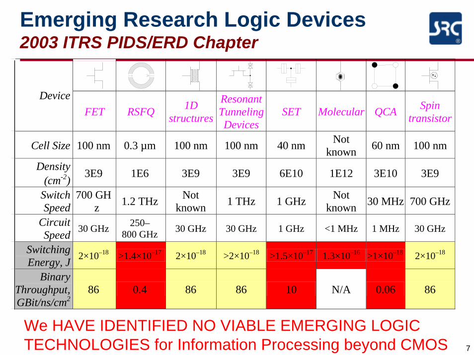
Emerging Research Logic Devices 2003 ITRS PIDS/ERD Chapter
Device
FET RSFQ 1D structures
Resonant Tunneling Devices
SET Molecular QCA Spin transistor
Cell Size 100 nm 0.3 µm 100 nm 100 nm 40 nm Not known 60 nm 100 nm
Density (cm-2) 3E9 1E6 3E9 3E9 6E10 1E12 3E10 3E9
Switch Speed
700 GHz 1.2 THz Not
known 1 THz 1 GHz Not known 30 MHz 700 GHz
Circuit Speed 30 GHz 250–
800 GHz 30 GHz 30 GHz 1 GHz <1 MHz 1 MHz 30 GHz
Switching Energy, J 2×10–18 >1.4×10⁻¹⁷ 2×10–18 >2×10–18 >1.5×10⁻¹⁷ 1.3×10⁻¹⁶ >1×10–18 2×10–18
Binary Throughput, GBit/ns/cm2
86 0.4 86 86 10 N/A 0.06 86
We HAVE IDENTIFIED NO VIABLE EMERGING LOGIC TECHNOLOGIES for Information Processing beyond CMOS
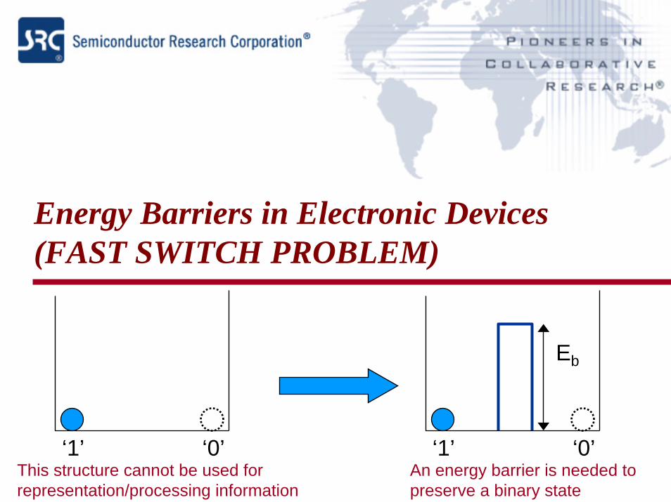
Energy Barriers in Electronic Devices(FAST SWITCH PROBLEM)
‘1’ ‘0’ ‘1’ ‘0’
Eb
This structure cannot be used for representation/processing information
An energy barrier is needed to preserve a binary state

9
Energy Barriers in MaterialsAny electronic device contains at least one energy barrier, which controls electron flow. The barrier properties, such as height, length, and shape determine the characteristics of electronic devices.
FET
Source: Y. Taur and T. H. Ning“Fundamentals of modern VLSI devices”Cambridge university Press 1998
R. Compano (Ed.)Technology Roadmap for Nanoelectronics(European Communities, 2001)
Resonant Tunnel Diode

10
Arbitrary Electronic Device
OFFWhat are the requirements/limitations on the height, width and shape of the barrier?ON

11
Classic Distinguishability: The Boltzman constraint
bbit EE =min
a
a
Eb
Eb
How small the energy barrier height could be ?
OREb
2ln
)exp(5.0
)exp(
min TkE
TkE
TkE
Bb
B
b
B
berror
=
−=
=Π
Distinguishability requirement: The probability of spontaneous transitions(errors) Πerror<0.5 (50%)
Barrier control (gate)

12
Quantum Distinguishability: The Heisenberg Constraint
2
22min
82ln
)22exp(
maE
Eam
b
bquantum
h
h
=
−=Π
aEb
aEb
Wigner-Kramers-Brillouin (WKB) approximation for tunneling:
h≥∆∆ px bcrit mE
a2h
=
2
2min
2~
maEb
h
(@Π=0.5)
(@Π=0.14)

13
Total Distinguishability @ Π=0.5
)22
exp()22exp()exp(kT
mEakTEEam
kTE bb
bb
quantumclassicquantumclassicerror
h
h
h
+−−−+−=
=ΠΠ−Π+Π=Π
0.60.70.80.9
11.11.2
0 5 10 15 20
a, nmE b/k
T
kTln2
Generalized expression for the minimum energy barrier to create a bit
2
22min
8)2(ln2ln
makTEb
h+≈

14
What does fundamental physics have to say about electron transport limits?
2lnmin TkE Bbit =1) Minimum energy per binary transition
2) Minimum distance between two distinguishable states (Heisenberg)
)300(5.12ln2min Knm
mkTax ===
hh≥∆∆ px
3) Minimum state switching time (Heisenberg)
)300(1042ln
14 KskT
tst−×==
hh≥∆∆ tE
213
2min
106.41cmgate
xn ×==4) Maximum gate density

15
Total Power Dissipation (@Ebit= kTln(2))
JTkEsJcm
tEnP
Bbit
bitchip
21
14
21213
1032ln][104][103][106.4
−
−
−−
⋅≈=
⋅⋅
⋅⋅=⋅
=
261074.4
cmWPchip ×= T=300 K
The circuit would vaporize when it is turned on!
16
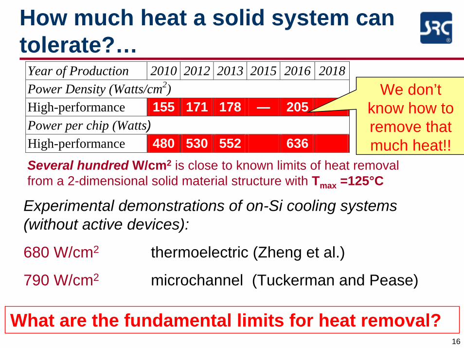
How much heat a solid system can tolerate?…
Year of Production 2010 2012 2013 2015 2016 2018Power Density (Watts/cm2) High-performance 155 171 178 — 205 — Power per chip (Watts) High-performance 480 530 552 636
Several hundred W/cm2 is close to known limits of heat removal from a 2-dimensional solid material structure with Tmax =125°C
We don’t know how to remove that much heat!!
Experimental demonstrations of on-Si cooling systems (without active devices):
680 W/cm2 thermoelectric (Zheng et al.)
790 W/cm2 microchannel (Tuckerman and Pease)
What are the fundamental limits for heat removal?

Should we consider cryogenic devices as an option for the mainstream applications?
Three fundamentals of heat removal:1)The Newton's Law of Cooling: q=h(Th-Ta) (h-heat transfer coefficient)
2) The Ambient: Ta=300 K !!!
3) The Carnot’s theorem:
−−= Q
TTTW
c
cacool
Heat to be removed
Work to be done

18
Cryogenic Computation with Nanodevices
2ln8
)2(ln2ln
8)2(ln2ln
2
22
2
22
aBdev
aaB
totalbit
devBdev
abit
dev
abit
dev
devabit
totalbit
TkmaT
TTkE
maTk
TTE
TTE
TTTEE
>+=
⎥⎦
⎤⎢⎣
⎡+==
−+=
h
h
10.00
100.00
1000.00
0 5 10 15 20
a, nm
E b, m
eV (t
otal
)
T=300K
T=4K
Due to tunneling, the power consumed by the device depends on both operating temperature and size that manifests itself with unexpectedly dramatic increases in total power consumption at cryogenic temperatures.

19
Asymptotically Dissipation-less Computing?
Often referred as to “reversible” or “adiabatic” computing…
We aren’t optimistic about Reversible or Adiabatic Computing:
Reversible Computing requires isolation from external environment
Cooling to very low temperature is very costly in terms of energy
“Adiabatic” methods attempt to save and re-use All proposed methods are inefficientRequire slow device operation for which there is limited interest

Some Current Ideas for Future Logic Devices
CNT and Nanowire transistorResonant tunneling devicesSingle electron transistorMolecular transistorSpintronics

21
CNT transistor
S. J. Wind,J. Appenzeller, R. Martel, V. Derycke, and Ph. Avouris,
Appl. Phys. Lett 80 (2002) 3817
Questions for CNT FETs1) Can CNT FET be smaller, faster and dissipate less energy than Si FET?
2) Is it possibilities to integrate individual CNT components in a complex circuit (billions of components per cm2)?
3) Is Ballistic Transport a big advantage?
vnej ⋅⋅=Fvdrift ⋅= µ
Ftmevb ⋅⎟
⎠⎞
⎜⎝⎛=
For long channels, is ballistic transport possible in the high-current regime?
ndrift>nbal

22
Single electron transistor
Single electron transistor (SET)Electron movements are controlled with single electron
precision Tunneling and Coulomb blockade
Single-Electron Transistor has all problems of charge-based devices
The Fan-Out requirement is not satisfied?
High error rate?
Low speed?
What about FET in single-electron mode? (FET will be 32-electron transistor by 2018)
source drain
island gate

23
Resonant tunneling devices(diodes and transistors)
1974 Chang1986 Reed1986 Reed1988 Broekaert1990 Broekaert1990 Mehdi1991 Chen1991 Smet1992 Watanabe1995 Moise1999 Miyamoto2000 Watanabe2001 Ishikawa2002 Kikuchi2002 Kado2002 Wernersson2002 Malindretos2002 Bjork2003 Wang2003 Ikeda2004 Xu
This year (2004) marks the 30 years of experimental studies of resonant tunneling structures (CHANG LL, ESAKI L, TSU R / IBM, “RESONANT TUNNELING IN SEMICONDUCTOR DOUBLE BARRIERS”, APPL. PHYS. LETT 24 (12): 593-595 1974)
Can RTDs match FETs both in ION and IOFF?
1.00E-07
1.00E-05
1.00E-03
1.00E-01
1.00E+01
1.00E+03
1.00E+05
1.00E+07
1 10 100 1000 10000 100000 1000000Peak-to-Valley Ratio
Jpea
k, A
/cm
2
FET
Jpeak
Jvalley

24
Molecular transistor
Molecular Transistor has all problems of charge-based devices
Question: Can molecular transistor be smaller, faster and dissipate less energy than Si FET?
Many fundamental issues in integration and fabrication
25
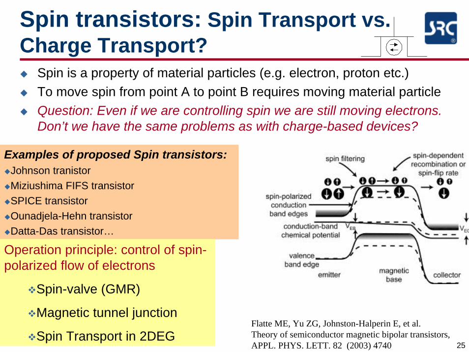
Spin transistors: Spin Transport vs. Charge Transport?
Spin is a property of material particles (e.g. electron, proton etc.)To move spin from point A to point B requires moving material particle Question: Even if we are controlling spin we are still moving electrons. Don’t we have the same problems as with charge-based devices?
Examples of proposed Spin transistors:Johnson tranistorMiziushima FIFS transistorSPICE transistorOunadjela-Hehn transistorDatta-Das transistor…
Operation principle: control of spin-polarized flow of electrons
Spin-valve (GMR)
Magnetic tunnel junction
Spin Transport in 2DEGFlatte ME, Yu ZG, Johnston-Halperin E, et al.Theory of semiconductor magnetic bipolar transistors, APPL. PHYS. LETT. 82 (2003) 4740

26
Which of current nanoelectronic concepts will become the NEW SWITCH?
QCA
RTD
Single Electronics
Molecular Electronics
RSFQ
Spintronics
1D-devices NEWSWITCH
ANSWER:
NONE YET
FILTER ???

What else could be done? Emerging Memory Devices
Invent high speed, high density, electrically accessible,non-volatile memory!

28
Memory and Logic in a typical computer system
CPU
Hard disk driveDensity-mediumCapacity-highSpeed-lowNon-Volatile
Density-highCapacity-highSpeed-highVolatile
Density-lowCapacity-mediumSpeed-highVolatile
Density-lowCapacity-lowSpeed-highVolatile
Main memory
2nd level cache
1st
level cache
SRAM
SRAM
DRAM
How can NVM enter this hierarchy?

29
Memory limits computer’s performance
Overall computer’s ability to execute programs are limited by interaction between MPU and memoryThis problem is not automatically solved by scaling
Evolutionary Solution: SRAM occupies increasing amount of floorspace of MPU chip – Less room for LOGIC
Decrease the net information throughputVolatility of semiconductor memory requires external storage media with slow access (magnetic hard drives, optical CD)
Invention of electrically accessible non-volatile memory with high speed and high density would imply a revolution in computer architectures

30
New Memory Hierarchy ?
CPU
Hard disk drive
Main memory
2nd level cache
1st
level cache
CPU
?Density-high
Capacity-highSpeed-highNon-Volatile
CPU
Density-highCapacity-high
Speed-highNon-Volatile
?
31
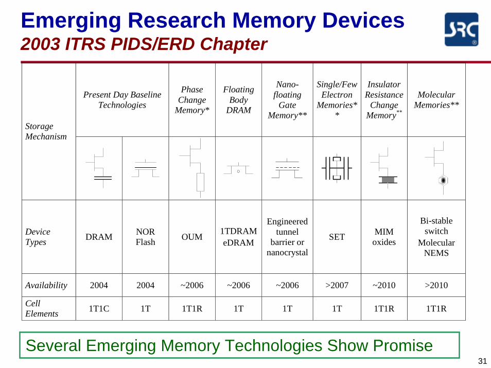
Emerging Research Memory Devices2003 ITRS PIDS/ERD Chapter
Present Day Baseline Technologies
Phase Change
Memory*
Floating Body
DRAM
Nano-floating
Gate Memory**
Single/Few Electron
Memories**
Insulator Resistance
Change Memory**
Molecular Memories**
Storage Mechanism
Device Types DRAM NOR
Flash OUM 1TDRAM eDRAM
Engineered tunnel
barrier or nanocrystal
SET MIM oxides
Bi-stable switch
Molecular NEMS
Availability 2004 2004 ~2006 ~2006 ~2006 >2007 ~2010 >2010
Cell Elements 1T1C 1T 1T1R 1T 1T 1T 1T1R 1T1R
Several Emerging Memory Technologies Show Promise

32
What Else Could be Done? –Explore new approaches
“Different” spintronics
Orbitronics
Phononics: thermal breakthrough
Invent high speed, high density, electrically accessible,non-volatile memory.
(1) How can we better remove heat and what are the fundamental limits of heat removal? (2) How can we isolate selected materials subsystems from thermal noise?(3) Are there ways to control phonon movement by external stimuli.Co-design of electric and thermal circuits?
(1) Can we make spin devices that operate without moving electrons? (2) Non-equilibrium operation of binary switch?
(1) Can we move atoms instead of moving electrons?
Interplay between charge, orbital, and spin degrees of freedom. Materials with both ferroelectricity and ferromagnetism (electrically controlled)