ssc clock generator/buffer - texas · pdf file1features applications package ssc_sel 0 1 8 vdd...
TRANSCRIPT

1FEATURES APPLICATIONS
PACKAGE
SSC_SEL 0
1 8 VDD
SSC_SEL 1
2 7
OUT
GND
3 6
SSC_ON
IN
4 5
CDCS501SSC_SEL 2
BLOCK DIAGRAMVDD GND
OUTSSC GeneratorIN LVCMOS
SPREAD
LOOK-UP
TABLE
SSC_SEL 0
SSC_SEL 1
SSC_SEL 2
LVCMOS
SSC_ON
DESCRIPTION
CDCS501
www.ti.com ..................................................................................................................................................................................................... SCAS874–APRIL 2009
SSC Clock Generator/Buffer
• Consumer and Industrial Applications• Part of a Family of Easy to use ClockRequiring EMI Reduction through SpreadGenerator Devices With Optional SSCSpectrum Clocking• SSC Capable Clock Generator / Buffer
• SSC Controllable via 3 External Pins– ±0% to ±1.5% Center Spread
• 1 External Control Pin for SSC ON / OFFSelection
• 40 MHz to 108 MHz Single-Ended LVCMOSInput
• Single 3.3V Device Power Supply• Wide Temperature Range – 40°C to 85°C• Low Space Consumption by 8 Pin TSSOP
Package
The CDCS501 is a spread spectrum capable, LVCMOS Input Clock Buffer for EMI reduction.
The device is designed to counter common EMI problems in modern electronic designs.
It accepts a 3.3V LVCMOS signal at the input and spread this signal by a small amount, centered around theinput frequency. The amount of spread can be selected via 3 control pins. The Functional Table contains detailedinformation on the amount of spread. A 4th control pin can be used to activate or deactivate the SpreadSpectrum Clock Generator.
Selecting SSC_ON = off will turn the Spread Spectrum Clock Generator off only. The device will still pass theLVCMOS signal that’s presented at its input trough to its output. This pin is low active.
The wide operating frequency range covers most commonly used midrange Audio and Video frequencies. TheCDCS501 operates in 3.3V environment.
It is characterized for operation from –40°C to 85°C, and available in an 8-pin TSSOP package.
1
Please be aware that an important notice concerning availability, standard warranty, and use in critical applications of TexasInstruments semiconductor products and disclaimers thereto appears at the end of this data sheet.
PRODUCTION DATA information is current as of publication date. Copyright © 2009, Texas Instruments IncorporatedProducts conform to specifications per the terms of the TexasInstruments standard warranty. Production processing does notnecessarily include testing of all parameters.

FUNCTION TABLE
DEVICE INFORMATION
PACKAGE
SSC_SEL 0
1 8 VDD
SSC_SEL 1
2 7
OUT
GND
3 6
SSC_ON
IN
4 5
CDCS501SSC_SEL 2
PACKAGE THERMAL RESISTANCE FOR TSSOP (PW) PACKAGE (1)
CDCS501
SCAS874–APRIL 2009..................................................................................................................................................................................................... www.ti.com
These devices have limited built-in ESD protection. The leads should be shorted together or the device placed in conductive foamduring storage or handling to prevent electrostatic damage to the MOS gates.
SSC_ON SSC_SEL 0 SSC_SEL 1 SSC_SEL 2 SPREAD AMOUNT1 x x X 0.00%0 0 0 0 1.00%0 0 0 1 1.50%0 0 1 0 1.00%0 0 1 1 1.50%0 1 0 0 0.50%0 1 0 1 0.75%0 1 1 0 0.00%0 1 1 1 0.50%
PIN FUNCTIONSPIN
NAME NO. Type DescriptionIN 1 I LVCMOS Clock InputOUT 6 O LVCMOS Clock OutputSSC_SEL 0, 1, 2 2, 3, 7 I Spread Selection Pins, internal Pull-upSSC_ON 5 I SSC on/off Pin, active low; internal Pull-downVDD 8 Power 3.3V Power SupplyGND 4 Ground Ground
THERMAL AIRFLOW (CFM)CDCS501PW 8-PIN TSSOP UNIT
0 150 250 500High K 149 142 138 132
RθJA °C / WLow K 230 185 170 150High K 65
RθJc °C / WLow K 69
(1) The package thermal impedance is calculated in accordance with JESD 51 and JEDEC2S2P (high-k board).
2 Submit Documentation Feedback Copyright © 2009, Texas Instruments Incorporated
Product Folder Link(s): CDCS501

ABSOLUTE MAXIMUM RATINGS (1)
RECOMMENDED OPERATING CONDITIONS
CDCS501
www.ti.com ..................................................................................................................................................................................................... SCAS874–APRIL 2009
over operating free-air temperature range (unless otherwise noted)
VALUE UNITVDD Supply voltage range –0.5 to 4.6 VVIN Input voltage range –0.5 to 4.6 VVout Output voltage range –0.5 to 4.6 VIIN Input current (VI < 0, VI > VDD) 20 mAIout Continuous output current 50 mATST Storage temperature range –65 to 150 °CTJ Maximum junction temperature 125 °C
(1) Stresses beyond those listed under absolute maximum ratings may cause permanent damage to the device. These are stress ratingsonly and functional operation of the device at these or any other conditions beyond those indicated under recommended operatingconditions is not implied. Exposure to absolute-maximum-rated conditions for extended periods may affect device reliability.
MIN NOM MAX UNITVDD Supply voltage 3.0 3.6 VfIN Input Frequency 40 108 MHzVIL Low level input voltage LVCMOS 0.3 VDD VVIH High level input voltage LVCMOS 0.7 VDD VVI Input Voltage threshold LVCMOS 0.5 VDD VCL Output Load Test LVCMOS 15 pFIOH/IOL Output Current 12 mATA Operating free-air temperature –40 85 °C
Copyright © 2009, Texas Instruments Incorporated Submit Documentation Feedback 3
Product Folder Link(s): CDCS501

DEVICE CHARACTERISTICS
10
15
20
25
30
35
40
20 30 40 50 60 70 80 90 100 110 120
f - Frequency - MHz
I-
Su
pp
ly C
urr
en
t -
mA
DD
V = 3.3 VDD
CDCS501
SCAS874–APRIL 2009..................................................................................................................................................................................................... www.ti.com
over recommended operating free-air temperature range (unless otherwise noted)
PARAMETER TEST CONDITIONS MIN TYP MAX UNITIDD Device supply current fIN = 80 MHz 26 mAfOUT Output frequency 40 108 MHzIIH LVCMOS input current VI = VDD; VDD = 3.6V 10 µAIIL LVCMOS input current VI = 0 V; VDD = 3.6V –10 µA
IOH = –0.1mA 2.9VOH LVCMOS high-level output voltage IOH = –8mA 2.4 V
IOH = –12mA 2.2IOL = 0.1mA 0.1
VOL LVCMOS low-level output voltage IOL = 8mA 0.5 VIOL = 12mA 0.8
tJIT(C-C) Cycle to cycle jitter cycles fout = 80 MHz; SSC = 1%, 10000 cycles 110 pstr/tf Rise and fall time 20%–80% 0.75 nsOdc Output duty cycle 45% 55%fMOD Modulation frequency 30 kHz
Figure 1. IDD vs. Input Frequency, VDD = 3.3V
4 Submit Documentation Feedback Copyright © 2009, Texas Instruments Incorporated
Product Folder Link(s): CDCS501

APPLICATION INFORMATION
SSC MODULATION
PARAMETER MEASUREMENT INFORMATION
VDD
1 kW
1 kW 10 pF
LVCMOS
CDCS501
LVCMOS LVCMOS
CDCS501
Typical DriverImpedance
~32 W
Series Termination
~18 W
Z = 50L W
CDCS501
www.ti.com ..................................................................................................................................................................................................... SCAS874–APRIL 2009
The exact implementation of the SSC modulation plays a vital role for the EMI reduction. The CDCS501 uses atriangular modulation scheme implemented in a way that the modulation frequency depends on the VCOfrequency of the internal PLL and the spread amount is independent from the VCO frequency.
The modulation frequency can be calculated by using the below formula.
fmod = fIN / 2480
Figure 2. Test Load
Figure 3. Test Load for 50-Ω Board Enviroment
Copyright © 2009, Texas Instruments Incorporated Submit Documentation Feedback 5
Product Folder Link(s): CDCS501

PACKAGE OPTION ADDENDUM
www.ti.com 25-Mar-2014
Addendum-Page 1
PACKAGING INFORMATION
Orderable Device Status(1)
Package Type PackageDrawing
Pins PackageQty
Eco Plan(2)
Lead/Ball Finish(6)
MSL Peak Temp(3)
Op Temp (°C) Device Marking(4/5)
Samples
CDCS501PW ACTIVE TSSOP PW 8 150 Green (RoHS& no Sb/Br)
CU NIPDAU Level-1-260C-UNLIM -40 to 85 CS501
CDCS501PWR ACTIVE TSSOP PW 8 2000 Green (RoHS& no Sb/Br)
CU NIPDAU Level-1-260C-UNLIM -40 to 85 CS501
(1) The marketing status values are defined as follows:ACTIVE: Product device recommended for new designs.LIFEBUY: TI has announced that the device will be discontinued, and a lifetime-buy period is in effect.NRND: Not recommended for new designs. Device is in production to support existing customers, but TI does not recommend using this part in a new design.PREVIEW: Device has been announced but is not in production. Samples may or may not be available.OBSOLETE: TI has discontinued the production of the device.
(2) Eco Plan - The planned eco-friendly classification: Pb-Free (RoHS), Pb-Free (RoHS Exempt), or Green (RoHS & no Sb/Br) - please check http://www.ti.com/productcontent for the latest availabilityinformation and additional product content details.TBD: The Pb-Free/Green conversion plan has not been defined.Pb-Free (RoHS): TI's terms "Lead-Free" or "Pb-Free" mean semiconductor products that are compatible with the current RoHS requirements for all 6 substances, including the requirement thatlead not exceed 0.1% by weight in homogeneous materials. Where designed to be soldered at high temperatures, TI Pb-Free products are suitable for use in specified lead-free processes.Pb-Free (RoHS Exempt): This component has a RoHS exemption for either 1) lead-based flip-chip solder bumps used between the die and package, or 2) lead-based die adhesive used betweenthe die and leadframe. The component is otherwise considered Pb-Free (RoHS compatible) as defined above.Green (RoHS & no Sb/Br): TI defines "Green" to mean Pb-Free (RoHS compatible), and free of Bromine (Br) and Antimony (Sb) based flame retardants (Br or Sb do not exceed 0.1% by weightin homogeneous material)
(3) MSL, Peak Temp. - The Moisture Sensitivity Level rating according to the JEDEC industry standard classifications, and peak solder temperature.
(4) There may be additional marking, which relates to the logo, the lot trace code information, or the environmental category on the device.
(5) Multiple Device Markings will be inside parentheses. Only one Device Marking contained in parentheses and separated by a "~" will appear on a device. If a line is indented then it is a continuationof the previous line and the two combined represent the entire Device Marking for that device.
(6) Lead/Ball Finish - Orderable Devices may have multiple material finish options. Finish options are separated by a vertical ruled line. Lead/Ball Finish values may wrap to two lines if the finishvalue exceeds the maximum column width.
Important Information and Disclaimer:The information provided on this page represents TI's knowledge and belief as of the date that it is provided. TI bases its knowledge and belief on informationprovided by third parties, and makes no representation or warranty as to the accuracy of such information. Efforts are underway to better integrate information from third parties. TI has taken andcontinues to take reasonable steps to provide representative and accurate information but may not have conducted destructive testing or chemical analysis on incoming materials and chemicals.TI and TI suppliers consider certain information to be proprietary, and thus CAS numbers and other limited information may not be available for release.

PACKAGE OPTION ADDENDUM
www.ti.com 25-Mar-2014
Addendum-Page 2
In no event shall TI's liability arising out of such information exceed the total purchase price of the TI part(s) at issue in this document sold by TI to Customer on an annual basis.

TAPE AND REEL INFORMATION
*All dimensions are nominal
Device PackageType
PackageDrawing
Pins SPQ ReelDiameter
(mm)
ReelWidth
W1 (mm)
A0(mm)
B0(mm)
K0(mm)
P1(mm)
W(mm)
Pin1Quadrant
CDCS501PWR TSSOP PW 8 2000 330.0 12.4 7.0 3.6 1.6 8.0 12.0 Q1
PACKAGE MATERIALS INFORMATION
www.ti.com 21-Apr-2016
Pack Materials-Page 1

*All dimensions are nominal
Device Package Type Package Drawing Pins SPQ Length (mm) Width (mm) Height (mm)
CDCS501PWR TSSOP PW 8 2000 367.0 367.0 35.0
PACKAGE MATERIALS INFORMATION
www.ti.com 21-Apr-2016
Pack Materials-Page 2

www.ti.com
PACKAGE OUTLINE
C
TYP6.66.2
1.2 MAX
6X 0.65
8X 0.300.19
2X1.95
0.150.05
(0.15) TYP
0 - 8
0.25GAGE PLANE
0.750.50
A
NOTE 3
3.12.9
BNOTE 4
4.54.3
4221848/A 02/2015
TSSOP - 1.2 mm max heightPW0008ASMALL OUTLINE PACKAGE
NOTES: 1. All linear dimensions are in millimeters. Any dimensions in parenthesis are for reference only. Dimensioning and tolerancing per ASME Y14.5M. 2. This drawing is subject to change without notice. 3. This dimension does not include mold flash, protrusions, or gate burrs. Mold flash, protrusions, or gate burrs shall not exceed 0.15 mm per side. 4. This dimension does not include interlead flash. Interlead flash shall not exceed 0.25 mm per side.5. Reference JEDEC registration MO-153, variation AA.
18
0.1 C A B
54
PIN 1 IDAREA
SEATING PLANE
0.1 C
SEE DETAIL A
DETAIL ATYPICAL
SCALE 2.800
www.ti.com
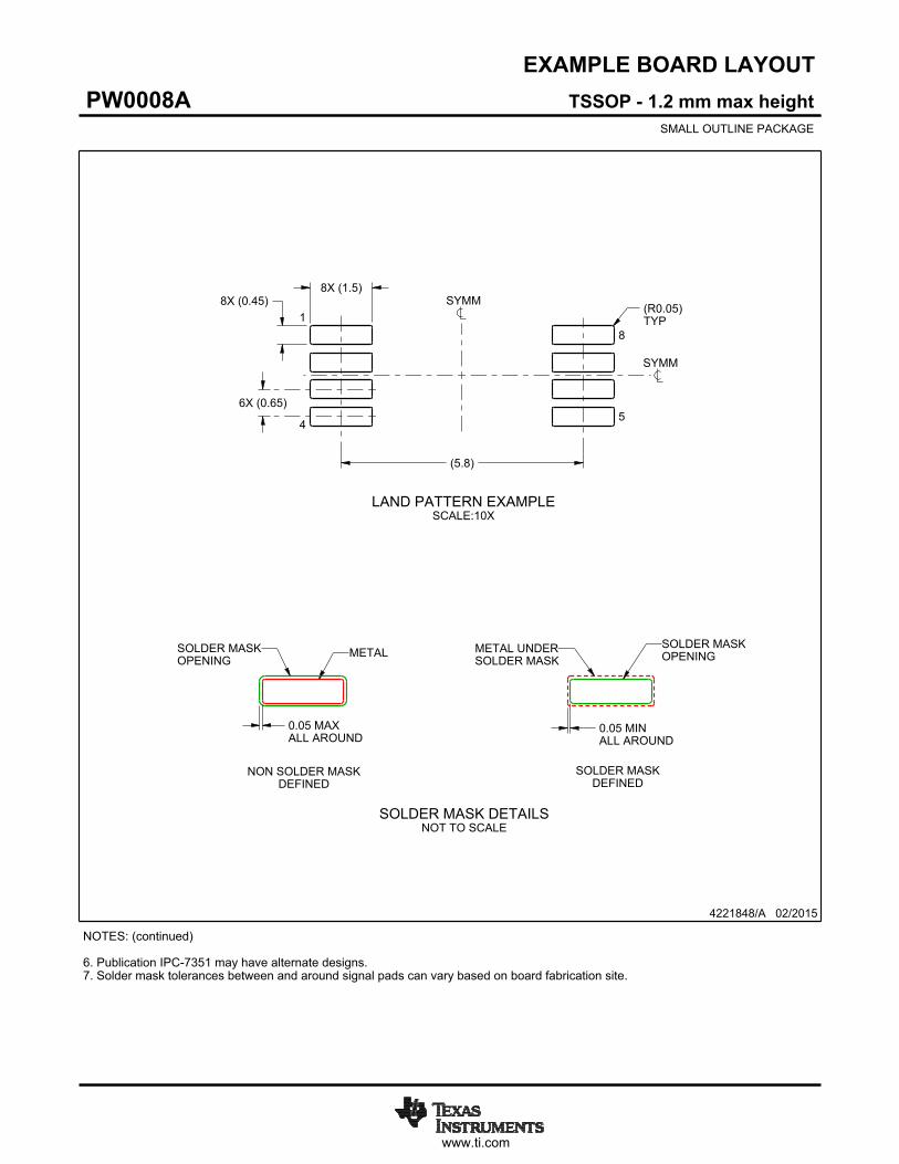
EXAMPLE BOARD LAYOUT
(5.8)
0.05 MAXALL AROUND
0.05 MINALL AROUND
8X (1.5)8X (0.45)
6X (0.65)
(R )TYP
0.05
4221848/A 02/2015
TSSOP - 1.2 mm max heightPW0008ASMALL OUTLINE PACKAGE
SYMM
SYMM
LAND PATTERN EXAMPLESCALE:10X
1
45
8
NOTES: (continued) 6. Publication IPC-7351 may have alternate designs. 7. Solder mask tolerances between and around signal pads can vary based on board fabrication site.
METALSOLDER MASKOPENING
NON SOLDER MASKDEFINED
SOLDER MASK DETAILSNOT TO SCALE
SOLDER MASKOPENING
METAL UNDERSOLDER MASK
SOLDER MASKDEFINED

www.ti.com
EXAMPLE STENCIL DESIGN
(5.8)
6X (0.65)
8X (0.45)8X (1.5)
(R ) TYP0.05
4221848/A 02/2015
TSSOP - 1.2 mm max heightPW0008ASMALL OUTLINE PACKAGE
NOTES: (continued) 8. Laser cutting apertures with trapezoidal walls and rounded corners may offer better paste release. IPC-7525 may have alternate design recommendations. 9. Board assembly site may have different recommendations for stencil design.
SYMM
SYMM
1
45
8
SOLDER PASTE EXAMPLEBASED ON 0.125 mm THICK STENCIL
SCALE:10X

IMPORTANT NOTICE
Texas Instruments Incorporated and its subsidiaries (TI) reserve the right to make corrections, enhancements, improvements and otherchanges to its semiconductor products and services per JESD46, latest issue, and to discontinue any product or service per JESD48, latestissue. Buyers should obtain the latest relevant information before placing orders and should verify that such information is current andcomplete. All semiconductor products (also referred to herein as “components”) are sold subject to TI’s terms and conditions of salesupplied at the time of order acknowledgment.TI warrants performance of its components to the specifications applicable at the time of sale, in accordance with the warranty in TI’s termsand conditions of sale of semiconductor products. Testing and other quality control techniques are used to the extent TI deems necessaryto support this warranty. Except where mandated by applicable law, testing of all parameters of each component is not necessarilyperformed.TI assumes no liability for applications assistance or the design of Buyers’ products. Buyers are responsible for their products andapplications using TI components. To minimize the risks associated with Buyers’ products and applications, Buyers should provideadequate design and operating safeguards.TI does not warrant or represent that any license, either express or implied, is granted under any patent right, copyright, mask work right, orother intellectual property right relating to any combination, machine, or process in which TI components or services are used. Informationpublished by TI regarding third-party products or services does not constitute a license to use such products or services or a warranty orendorsement thereof. Use of such information may require a license from a third party under the patents or other intellectual property of thethird party, or a license from TI under the patents or other intellectual property of TI.Reproduction of significant portions of TI information in TI data books or data sheets is permissible only if reproduction is without alterationand is accompanied by all associated warranties, conditions, limitations, and notices. TI is not responsible or liable for such altereddocumentation. Information of third parties may be subject to additional restrictions.Resale of TI components or services with statements different from or beyond the parameters stated by TI for that component or servicevoids all express and any implied warranties for the associated TI component or service and is an unfair and deceptive business practice.TI is not responsible or liable for any such statements.Buyer acknowledges and agrees that it is solely responsible for compliance with all legal, regulatory and safety-related requirementsconcerning its products, and any use of TI components in its applications, notwithstanding any applications-related information or supportthat may be provided by TI. Buyer represents and agrees that it has all the necessary expertise to create and implement safeguards whichanticipate dangerous consequences of failures, monitor failures and their consequences, lessen the likelihood of failures that might causeharm and take appropriate remedial actions. Buyer will fully indemnify TI and its representatives against any damages arising out of the useof any TI components in safety-critical applications.In some cases, TI components may be promoted specifically to facilitate safety-related applications. With such components, TI’s goal is tohelp enable customers to design and create their own end-product solutions that meet applicable functional safety standards andrequirements. Nonetheless, such components are subject to these terms.No TI components are authorized for use in FDA Class III (or similar life-critical medical equipment) unless authorized officers of the partieshave executed a special agreement specifically governing such use.Only those TI components which TI has specifically designated as military grade or “enhanced plastic” are designed and intended for use inmilitary/aerospace applications or environments. Buyer acknowledges and agrees that any military or aerospace use of TI componentswhich have not been so designated is solely at the Buyer's risk, and that Buyer is solely responsible for compliance with all legal andregulatory requirements in connection with such use.TI has specifically designated certain components as meeting ISO/TS16949 requirements, mainly for automotive use. In any case of use ofnon-designated products, TI will not be responsible for any failure to meet ISO/TS16949.
Products ApplicationsAudio www.ti.com/audio Automotive and Transportation www.ti.com/automotiveAmplifiers amplifier.ti.com Communications and Telecom www.ti.com/communicationsData Converters dataconverter.ti.com Computers and Peripherals www.ti.com/computersDLP® Products www.dlp.com Consumer Electronics www.ti.com/consumer-appsDSP dsp.ti.com Energy and Lighting www.ti.com/energyClocks and Timers www.ti.com/clocks Industrial www.ti.com/industrialInterface interface.ti.com Medical www.ti.com/medicalLogic logic.ti.com Security www.ti.com/securityPower Mgmt power.ti.com Space, Avionics and Defense www.ti.com/space-avionics-defenseMicrocontrollers microcontroller.ti.com Video and Imaging www.ti.com/videoRFID www.ti-rfid.comOMAP Applications Processors www.ti.com/omap TI E2E Community e2e.ti.comWireless Connectivity www.ti.com/wirelessconnectivity
Mailing Address: Texas Instruments, Post Office Box 655303, Dallas, Texas 75265Copyright © 2016, Texas Instruments Incorporated