steeper: tunnel field effect transistors (tfets)
TRANSCRIPT

STEEPER: Tunnel Field Effect Transistors (TFETs) Technology, Devices and Applications
Thomas Schulz, Reinhard Mahnkopf Intel Mobile Communications (IMC) MOS-AK/GSA Workshop 12.04.13, Munich

Outline
April 26, 2013 2
1. The STEEPER Project
3. TFET Devices
2. TFET Technology
4. TFET Applications
The Material presented in this presentation is public or STEEPER project confidential and intended for the registered addressee(s) of the MOS-AK/GSA Workshop 12.04.13 in Munich, only. Further distribution is not allowed.

Outline
April 26, 2013 3
1. The STEEPER Project
3. TFET Devices
2. TFET Technology
4. TFET Applications

• http://www.steeper-project.org/
STEEPER is a major European research initiative addressing the alarming growth of energy consumption by electronic devices, ranging from mobile phones to laptops to televisions to supercomputers. STEEPER aims to increase the energy efficiency of these devices, when active, by 10 times and virtually eliminate power consumption when they are in passive or standby mode.
STEEPER Project Website
April 26, 2013 4

GENERAL
• OBJ 1: Demonstrate energy efficient steep subthreshold slope transistors based on quantum mechanical band‐to‐band tunneling (tunnel FETs) able to reduce the voltage operation of advanced nanoelectronic circuits into sub‐0.5V and their power consumption by one order of magnitude.
• OBJ 2: Enable and demonstrate the power consumption benefits resulting from hybridization of tunnel FET and CMOS technologies and from tunnel FETs as standalone technology for digital, analog, RF and mixed‐mode circuit applications.
TECHNOLOGY
• OBJ 3: Develop a CMOS‐compatible UTB SOI technology platform for tunnel FETs with ultralow standby power by exploiting key additive boosters for enhanced performance: high-k dielectrics, SiGe source, strain.
• OBJ 4: Study and identify advanced technology implementations for high‐Ion tunnel FETs: III‐V materials, nanowires, staggered versus broken band gaps, electrostatic doping.
Project Objectives 1
April 26, 2013 5

SIMULATION and MODELLING
• OBJ 5: Develop accurate numerical simulation tools: semi‐classical multi‐sub‐band Monte Carlo simulator and full‐band quantum‐transport simulation for in‐depth study of UTB and nanowire tunnel FETs, respectively.
• • OBJ 6: Study the scaling, parameter sensitivity and variability on the characteristics of nanometer tunnel FETs.
• • OBJ 7: Develop and implement DC and AC compact models for the simulation and design of circuits based on tunnel FETs and or co‐design with advanced CMOS.
INDUSTRIAL BENCHMARKING
• OBJ 8: Benchmark tunnel FETs developed in STEEPER for low standby power logic, high speed, memory, RF and analog applications. Evaluate their energy efficiency against CMOS.
Project Objectives 2
April 26, 2013 6

• 3 industries, 2 research institutes, 5 universities, 1 SME
• 4 countries: Germany, France, Italy, Switzerland.
TECHNOLOGY
Laboratoire d`Electronique et de Technologie de l`Information (LETI)
IBM Research GmbH (IBM)
Research Center Juelich (FZJ)
SIMULATION and MODELLING
Ecole Polytechnique Fédérale de Lausanne (EPFL)
Consorzio Nazionale Interuniversitario per la Nanoelectronica (IUNET)
RWTH Aachen University (RWTH)
INDUSTRIAL BENCHMARKING
GlobalFoundries (GF)
Intel Mobile Communications (IMC)
Project Partners
April 26, 2013 7

Goal: Progress beyond state-of-the-art
April 26, 2013 8

Tunnel FET concept:
Beyond CMOS devices
April 26, 2013 9
Tunnel FET features:
+ Steeper subthreshold slope
+ Less OFF current
- Less ON current

Outline
April 26, 2013 10
1. The STEEPER Project
2. TFET Technology
3. TFET Devices
4. TFET Applications

• Planar SOI CMOS with planar Si TF
• Planar bulk CMOS with vertical III-V TFET
Two generic hybrid CMOS-TFET processes
April 26, 2013 11

1. SOI substrate and shallow trench isolation (STI)
Planar SOI CMOS with Si TFET
April 26, 2013 12

2. Channel implantations
Planar SOI CMOS with Si TFET
April 26, 2013 13

3. Multi-layer Gatestack deposition
Planar SOI CMOS with Si TFET
April 26, 2013 14

4. Gatestack etch
Planar SOI CMOS with Si TFET
April 26, 2013 15

5. Gate liner deposition
Planar SOI CMOS with Si TFET
April 26, 2013 16

6. Gate liners as spacer etch formation
Planar SOI CMOS with Si TFET
April 26, 2013 17

7. First epitaxial layers for LDD preparation
Planar SOI CMOS with Si TFET
April 26, 2013 18

8. LDD implantations
Planar SOI CMOS with Si TFET
April 26, 2013 19

9. Second epitaxial layers for HDD preparation
Planar SOI CMOS with Si TFET
April 26, 2013 20

10. Second gate spacer for HDD preparation
Planar SOI CMOS with Si TFET
April 26, 2013 21

11. Silicide blocking for TFET option
Planar SOI CMOS with Si TFET
April 26, 2013 22

12. Source/Drain HDD implantations
Planar SOI CMOS with Si TFET
April 26, 2013 23

13. Silicidation
Planar SOI CMOS with Si TFET
April 26, 2013 24

14. Dual stress liner
Planar SOI CMOS with Si TFET
April 26, 2013 25

15. Planarization for BEOL
Planar SOI CMOS with Si TFET
April 26, 2013 26

16. Contacts etch
Planar SOI CMOS with Si TFET
April 26, 2013 27

17. Metal 1 formation
Planar SOI CMOS with Si TFET
April 26, 2013 28

18. Dual damascene via 1 and metal 2
Planar SOI CMOS with Si TFET
April 26, 2013 29

Ref.: A. Villalon et. al. «Strained Tunnel FETs with record ION: First demonstration of ETSOI TFETs with SiGe channel and RSD», Symposia on VLSI Technology and Circuits 2012
Experimental TFET (LETI)
April 26, 2013 30
BOX
P+ N+
VS=0 VD>0
VG>0
VG > 0
EC
EV
N mode P mode
VG < 0
BOX
P+ N+
VD<0 VS=0
VG<0
ID>0 ID<0
e- e-
EC
EV
BOX
Gate Si0.7Ge0.3
RSD silicide
P+
N+
Sicap cSiGe Si
strain mapping

TFET Reliability - Tradeoffs
31
• Variability vs. Performance/Drivability (?) • Simulated Id-Vg with uniform but
different concentrations of source doping *
„ideal“ device with steep sub-Vt slope exhibits device mismatch, e.g. current onset or max. drive current „real“ device implementation leads to sub-Vt slope degradation
* P. Patel, K. Jeon, A. Bowonder and C.Hu, SISPAD 2009
* C.Hu, et. al., IEDM 2009
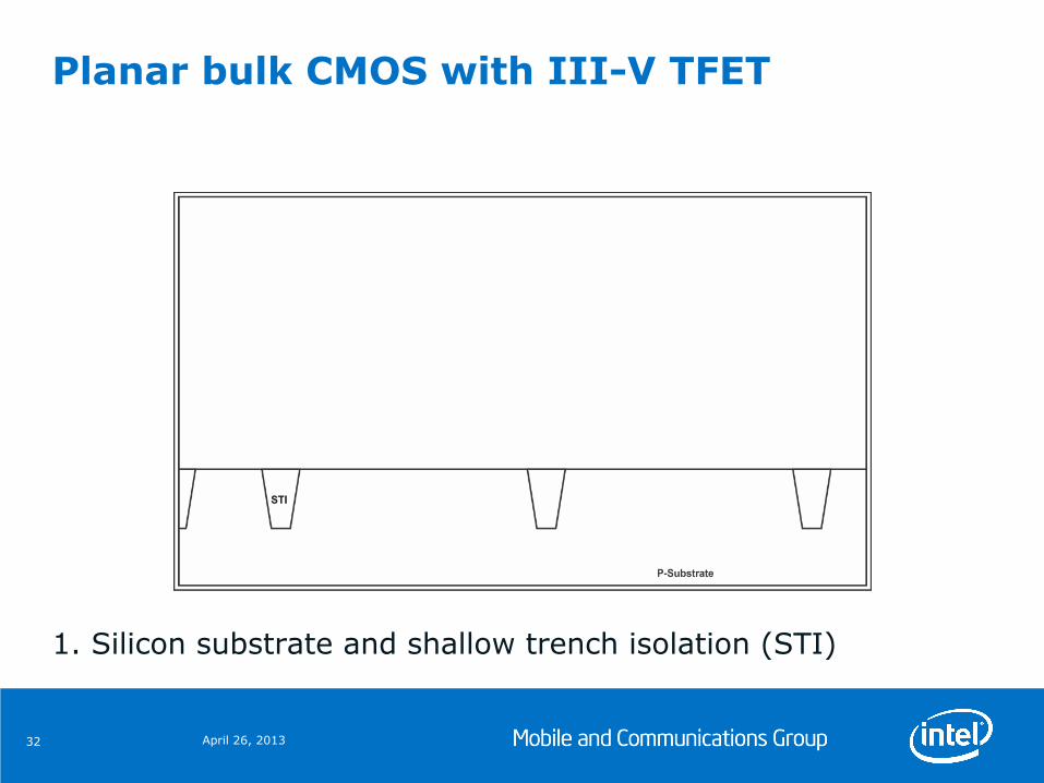
1. Silicon substrate and shallow trench isolation (STI)
Planar bulk CMOS with III-V TFET
April 26, 2013 32

2. Deep N-Band implantation
Planar bulk CMOS with III-V TFET
April 26, 2013 33

3. P-Well and N-Well implantations
Planar bulk CMOS with III-V TFET
April 26, 2013 34

4. Retrograde well and channel implantations
Planar bulk CMOS with III-V TFET
April 26, 2013 35

5. Multi-layer Gatestack deposition
Planar bulk CMOS with III-V TFET
April 26, 2013 36

6. Gatestack etch
Planar bulk CMOS with III-V TFET
April 26, 2013 37
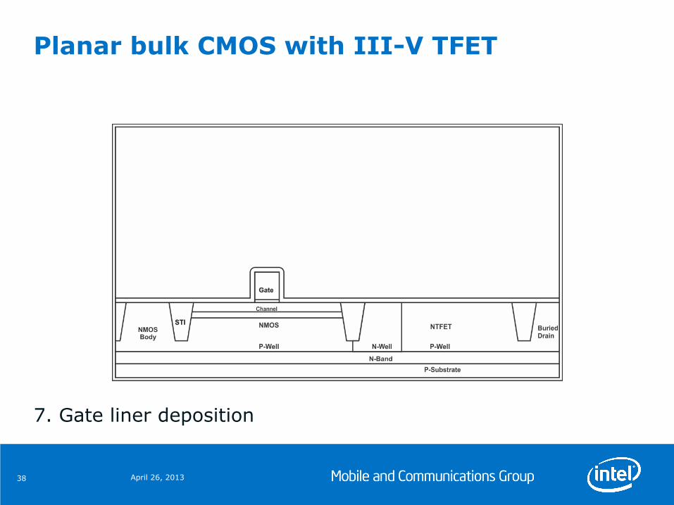
7. Gate liner deposition
Planar bulk CMOS with III-V TFET
April 26, 2013 38

8. Gate liners as spacer etch formation
Planar bulk CMOS with III-V TFET
April 26, 2013 39

9. Source/Drain LDD and Pocket implantations
Planar bulk CMOS with III-V TFET
April 26, 2013 40

10. Source/Drain etches for eSiC/eSiGe preparation
Planar bulk CMOS with III-V TFET
April 26, 2013 41

11. Elevated Source/Drain eSiC/eSiGe epitaxial layers
Planar bulk CMOS with III-V TFET
April 26, 2013 42

12. 2nd Gate Spacer
Planar bulk CMOS with III-V TFET
April 26, 2013 43

13. Source/Drain HDD and body access implantations
Planar bulk CMOS with III-V TFET
April 26, 2013 44

14. Source/Drain and Gate silicidation
Planar bulk CMOS with III-V TFET
April 26, 2013 45

15. CMOS part cover
Planar bulk CMOS with III-V TFET
April 26, 2013 46

16. Shallow trench etch for TFET epitaxial layers seed
Planar bulk CMOS with III-V TFET
April 26, 2013 47

17. TFET epitaxial layers
Planar bulk CMOS with III-V TFET
April 26, 2013 48

18. TFET pillar etch
Planar bulk CMOS with III-V TFET
April 26, 2013 49

19. TFET bottom gate isolation layer deposition
Planar bulk CMOS with III-V TFET
April 26, 2013 50

20. Recess of bottom gate isolation
Planar bulk CMOS with III-V TFET
April 26, 2013 51

21. Deposition of gatestack
Planar bulk CMOS with III-V TFET
April 26, 2013 52

22. Recess of gatestack
Planar bulk CMOS with III-V TFET
April 26, 2013 53

23. TFET top gate isolation layer deposition
Planar bulk CMOS with III-V TFET
April 26, 2013 54
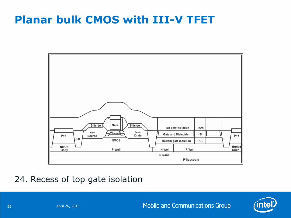
24. Recess of top gate isolation
Planar bulk CMOS with III-V TFET
April 26, 2013 55

25. Etch and fill of Gate access plug
Planar bulk CMOS with III-V TFET
April 26, 2013 56

26. CMOS part open
Planar bulk CMOS with III-V TFET
April 26, 2013 57

27. Dual stress liner
Planar bulk CMOS with III-V TFET
April 26, 2013 58

28. Planarization for BEOL
Planar bulk CMOS with III-V TFET
April 26, 2013 59

29. Contacts etch
Planar bulk CMOS with III-V TFET
April 26, 2013 60

30.Metal 1 formation
Planar bulk CMOS with III-V TFET
April 26, 2013 61
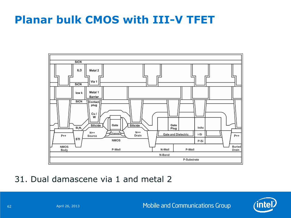
31. Dual damascene via 1 and metal 2
Planar bulk CMOS with III-V TFET
April 26, 2013 62
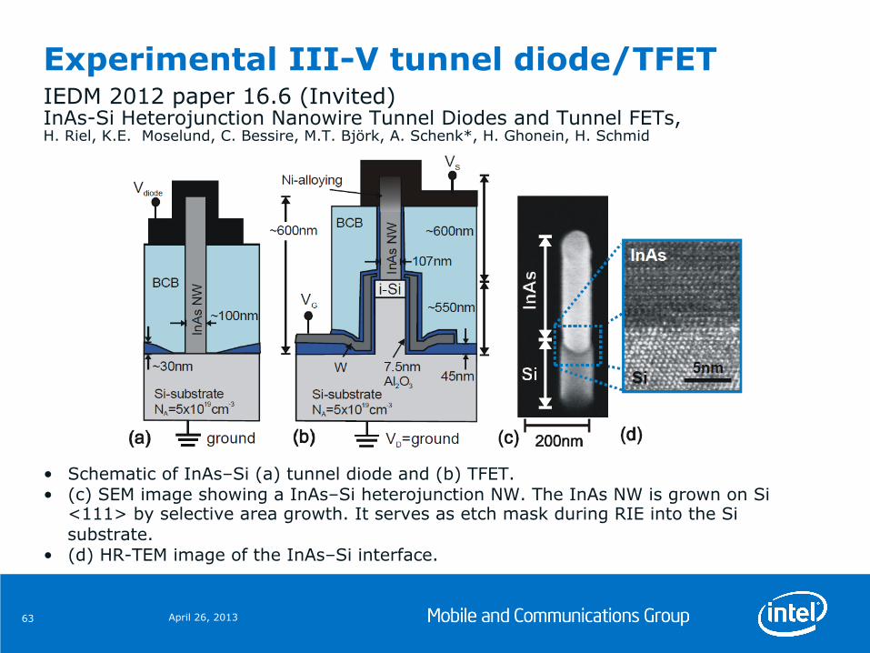
IEDM 2012 paper 16.6 (Invited) InAs-Si Heterojunction Nanowire Tunnel Diodes and Tunnel FETs, H. Riel, K.E. Moselund, C. Bessire, M.T. Björk, A. Schenk*, H. Ghonein, H. Schmid
• Schematic of InAs–Si (a) tunnel diode and (b) TFET. • (c) SEM image showing a InAs–Si heterojunction NW. The InAs NW is grown on Si
<111> by selective area growth. It serves as etch mask during RIE into the Si substrate.
• (d) HR-TEM image of the InAs–Si interface.
Experimental III-V tunnel diode/TFET
April 26, 2013 63

Trap-assisted tunneling due to defect states
April 26, 2013 64
Trap-assisted tunneling in InAs–Si heterojunction tunnel diodes (ND = 5·1017 cm-3, NA = 1·1020 cm-3). The second derivative of current with respect to voltage was measured at 4.2 K. Pronounced peaks in forward bias originate from trap-assisted tunneling due to defect states in the bandgap. In reverse bias peaks are less distinct.

Aspect Ratio Trapping (ART)
April 26, 2013 65
Ref.: J. G. Fiorenza, et. al., “Aspect Ratio Trapping: a Unique Technology for Integrating Ge and III-Vs with Silicon CMOS”, ECS Transactions, 33 (6) 963-976 (2010), 10.1149/1.3487628 © The Electrochemical Society
A Si-III-V epitaxie might be a shortcoming of the III-V Tunnel-FET device concept. The epi interface is the most sensitive area of the device because here the tunnel junction is located. But at the same time this interface is the origin of random crystallographic defects like dislocations and stacking faults due to the lattice mismatch of the materials. Even if the Si/III-V pillar looks perfect from the outside there might be a crystallographic defect at the tunnel interface which makes the electrical function of this device fail. An improvement might be the ART concept where stacking faults are directed into vertical sidewalls.

Outline
April 26, 2013 66
3. TFET Devices
2. TFET Technology
4. TFET Applications
1. The STEEPER Project

TFET Benchmarking – ITRS
67
• Benchmarking ERD/ITRS 2009 spider chart • The rating means
– 1) Substantially (2×) inferior to ultimately scaled CMOS – 2) Comparable to ultimately scaled CMOS – 3) Substantially exceeds ultimately scaled CMOS

Lmask = 40nm, W=80nm DIBLp = 64 mV/V SSsat,p = 70 mV/dec
Co-integrated FDSOI CMOS and TFET (LETI)
April 26, 2013 68
pFET performance better than nFET in agreement with SiGe properties Ref.: A. Villalon et. al. Symposia on VLSI Technology and Circuits 2012

We have demonstrated InAs-Si vertical heterojunction NW tunnel diodes with record high currents of 6MA/cm2 at 0.5 V in reverse bias and TFETs with 2.4 µA/µm, Ion/Ioff 10^6 and a slope of 150 mV/dec over 3 decades. The achieved improvements can be attributed to increased NW doping and Ni alloying of the top contact.
III-V TD/TFET (IBM)
April 26, 2013 69
NWdiameter=130nm Vbias=0.5V
Experiment
Simulation

The steepest SS measured over two decades in current was 120 and 150 mV/dec over three decades in current measured, on several devices.
III-V TFET (IBM)
April 26, 2013 70
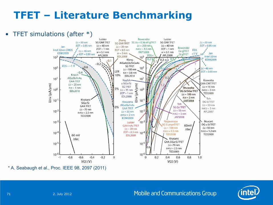
TFET – Literature Benchmarking
2. July 2012 71
* A. Seabaugh et al., Proc. IEEE 98, 2097 (2011)
• TFET simulations (after *)

2. July 2012 72
TFET – Literature Benchmarking
* A. Seabaugh et al., Proc. IEEE 98, 2097 (2011)
• TFET experimental data (after *)

This work: STEEPER (IBM, IEDM 2012)
Benchmark: III-V TFET update
April 26, 2013 73
Advanced CMOS area

Simulated Ion scaling by: a) Gate oxide thickness b) Device body thickness c) Tunnel barrier height lowering d) Combination of a)+b)+c)
III-V TFET (Intel, G. Dewey IEDM 2011, VLSI 2012)
April 26, 2013 74

Outline
April 26, 2013 75
3. TFET Devices
4. TFET Applications
2. TFET Technology
1. The STEEPER Project

Analog Device Parameter - General
76
• Analog/RF • benefits from faster devices & digital enhanced concepts • suffers from
– analog voltage headroom reduction
– analog gain reduction
– reduced signal to noise ratio – available power (e.g. in 50Ω)
– dynamic range reduction
CMOS Analog Performance - Transistor as Voltage Amplifier
- Intrinsic voltage gain
depends on geometry and bias conditions

Analog Device Parameter
77
• Benchmarking: TFET vs. planar CMOS logic (28nm)
* geometries for CMOS devices only
• data @ VD=0.5*VDmax, VG=VT+0.2V • extraction of TFET parameters difficult, esp. gds; little data/not accurate due to curve shifts

Target Application Space
78
• energy efficient nanoelectronic systems for high volume markets covering digital, analog/RF and mixed mode applications
• status today: • computation-intensive applications are still implemented best in advanced CMOS • new niche markets for TFET technologies ?
– slower, but much more energy efficient than CMOS à battery liftime limited applications with low activity & speed (e.g. M2M)
• Product segments/applications which might benefit from STEEPER/TFET technology in future – Industrial metering – Telemetry – Asset & vehicle tracking – Wireless security systems – ...
e.g. state-of-the-art product examples from Dr. Neuhaus, GenX Mobile, and Jablocom EyeSee 3G Security Camera

These results have been achieved by the different partners in the European project STEEPER. Many thanks to:
Laboratoire d`Electronique et de Technologie de l`Information (LETI)
IBM Research GmbH (IBM)
Research Center Juelich (FZJ)
RWTH Aachen University (RWTH)
Ecole Polytechnique Fédérale de Lausanne (EPFL)
Consorzio Nazionale Interuniversitario per la Nanoelectronica (IUNET)
GlobalFoundries (GF)
Intel Mobile Communications (IMC)
Acknowledgement
April 26, 2013 79
