stereo 3.1w class d amplifier - maxim integrated - analog ... · input voltage high vinh vpvdd =...
TRANSCRIPT

_______________________________________________________________ Maxim Integrated Products 1
For pricing, delivery, and ordering information, please contact Maxim Direct at 1-888-629-4642, or visit Maxim’s website at www.maxim-ic.com.
MA
X9
83
03
Stereo 3.1W Class D Amplifier
General DescriptionThe MAX98303 stereo 3.1W Class D amplifier provides Class AB audio performance with Class D efficiency. This device offers five selectable gain settings (6dB, 9dB, 12dB, 15dB, and 18dB) set by a single gain-select input (GAIN).
Active emissions limiting, edge-rate, and overshoot con-trol circuitry greatly reduces EMI. A filterless spread-spectrum modulation scheme eliminates the need for output filtering found in traditional Class D devices. These features reduce application component count.
The IC's 2.0mA at 3.7V, 2.7mA at 5V, quiescent current extends battery life in portable applications.
The IC is available in a 16-bump WLP (1.68mm x 1.68mm x 0.64mm) package specified over the extended -40NC to +85NC temperature range.
Applications
FeaturesS Low Quiescent Current: 2.0mA at 3.7V, 2.7mA
at 5V
S Spread Spectrum and Active Emissions Limiting
S Five Pin-Selectable Gains
S Click-and-Pop Suppression
S Thermal and Overcurrent Protection
S Low-Current Shutdown Mode
S Space-Saving, 1.68mm x 1.68mm x 0.64mm, 16-Bump WLP (0.4mm Pitch)
19-5494; Rev 0; 9/10
+Denotes a lead(Pb)-free/RoHS-compliant package.
Ordering Information
Typical Application Circuit
Notebook and Netbook Computers
Tablets
Cellular Phones
MP3 Players
Portable Audio Players
VoIP Phones
EVALUATION KIT
AVAILABLE
INL+ OUTL+
OUTL-
OUTR-
OUTR+
INL-
INR-
INR+
GAIN GAINCONTROL
1µF
1µF
1µF
1µF
PVDD
PVDD
PGNDSHDN
MAX98303
0.1µF 10µF
+2.6V TO +5.5V
PVDD
PARTTEMP
RANGEPIN-
PACKAGETOP
MARK
MAX98303EWE+-40NC to +85NC
16 WLP AAA
2 ______________________________________________________________________________________
MA
X9
83
03
Stereo 3.1W Class D Amplifier
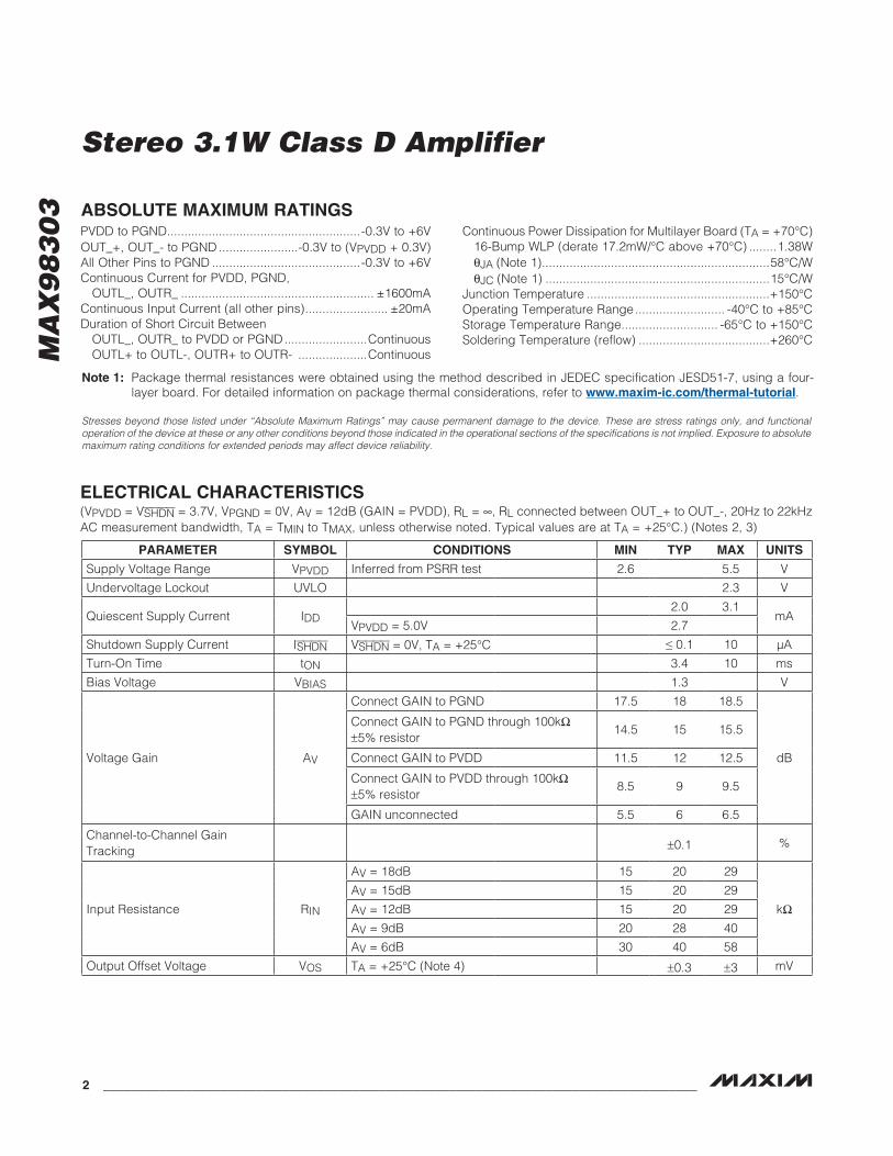
Stresses beyond those listed under “Absolute Maximum Ratings” may cause permanent damage to the device. These are stress ratings only, and functional operation of the device at these or any other conditions beyond those indicated in the operational sections of the specifications is not implied. Exposure to absolute maximum rating conditions for extended periods may affect device reliability.
PVDD to PGND ........................................................-0.3V to +6VOUT_+, OUT_- to PGND .......................-0.3V to (VPVDD + 0.3V)All Other Pins to PGND ...........................................-0.3V to +6VContinuous Current for PVDD, PGND, OUTL_, OUTR_ ........................................................Q1600mAContinuous Input Current (all other pins) ........................Q20mADuration of Short Circuit Between OUTL_, OUTR_ to PVDD or PGND ........................Continuous OUTL+ to OUTL-, OUTR+ to OUTR- ....................Continuous
Continuous Power Dissipation for Multilayer Board (TA = +70NC) 16-Bump WLP (derate 17.2mW/NC above +70NC) ........1.38W BJA (Note 1) ..................................................................58NC/W BJC (Note 1) .................................................................15NC/WJunction Temperature .....................................................+150NCOperating Temperature Range .......................... -40NC to +85NCStorage Temperature Range ............................ -65NC to +150NCSoldering Temperature (reflow) ......................................+260NC
ELECTRICAL CHARACTERISTICS(VPVDD = VSHDN = 3.7V, VPGND = 0V, AV = 12dB (GAIN = PVDD), RL = J, RL connected between OUT_+ to OUT_-, 20Hz to 22kHz AC measurement bandwidth, TA = TMIN to TMAX, unless otherwise noted. Typical values are at TA = +25NC.) (Notes 2, 3)
ABSOLUTE MAXIMUM RATINGS
Note 1: Package thermal resistances were obtained using the method described in JEDEC specification JESD51-7, using a four-layer board. For detailed information on package thermal considerations, refer to www.maxim-ic.com/thermal-tutorial.
PARAMETER SYMBOL CONDITIONS MIN TYP MAX UNITS
Supply Voltage Range VPVDD Inferred from PSRR test 2.6 5.5 V
Undervoltage Lockout UVLO 2.3 V
Quiescent Supply Current IDD2.0 3.1
mAVPVDD = 5.0V 2.7
Shutdown Supply Current ISHDN VSHDN = 0V, TA = +25NC ≤ 0.1 10 FA
Turn-On Time tON 3.4 10 ms
Bias Voltage VBIAS 1.3 V
Voltage Gain AV
Connect GAIN to PGND 17.5 18 18.5
dB
Connect GAIN to PGND through 100kI ±5% resistor
14.5 15 15.5
Connect GAIN to PVDD 11.5 12 12.5
Connect GAIN to PVDD through 100kI ±5% resistor
8.5 9 9.5
GAIN unconnected 5.5 6 6.5
Channel-to-Channel Gain Tracking ±0.1 %
Input Resistance RIN
AV = 18dB 15 20 29
kI
AV = 15dB 15 20 29
AV = 12dB 15 20 29
AV = 9dB 20 28 40
AV = 6dB 30 40 58
Output Offset Voltage VOS TA = +25NC (Note 4) ±0.3 ±3 mV
_______________________________________________________________________________________ 3
MA
X9
83
03
Stereo 3.1W Class D Amplifier
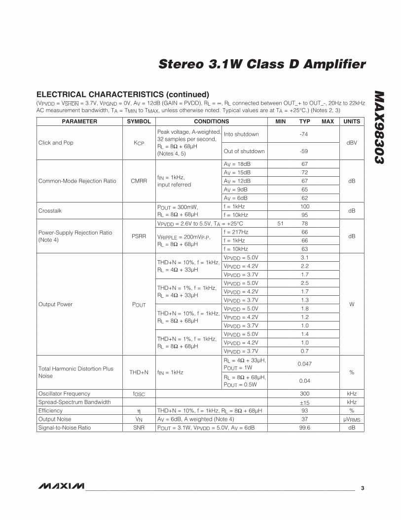
ELECTRICAL CHARACTERISTICS (continued)(VPVDD = VSHDN = 3.7V, VPGND = 0V, AV = 12dB (GAIN = PVDD), RL = J, RL connected between OUT_+ to OUT_-, 20Hz to 22kHz AC measurement bandwidth, TA = TMIN to TMAX, unless otherwise noted. Typical values are at TA = +25NC.) (Notes 2, 3)
PARAMETER SYMBOL CONDITIONS MIN TYP MAX UNITS
Click and Pop KCP
Peak voltage, A-weighted, 32 samples per second, RL = 8I + 68FH (Notes 4, 5)
Into shutdown -74
dBV
Out of shutdown -59
Common-Mode Rejection Ratio CMRRfIN = 1kHz, input referred
AV = 18dB 67
dB
AV = 15dB 72
AV = 12dB 67
AV = 9dB 65
AV = 6dB 62
CrosstalkPOUT = 300mW,RL = 8I + 68FH
f = 1kHz 100dB
f = 10kHz 95
Power-Supply Rejection Ratio (Note 4)
PSRR
VPVDD = 2.6V to 5.5V, TA = +25NC 51 78
dBVRIPPLE = 200mVP-P,RL = 8I + 68FH
f = 217Hz 66
f = 1kHz 66
f = 10kHz 63
Output Power POUT
THD+N = 10%, f = 1kHz, RL = 4I + 33µH
VPVDD = 5.0V 3.1
W
VPVDD = 4.2V 2.2
VPVDD = 3.7V 1.7
THD+N = 1%, f = 1kHz, RL = 4I + 33µH
VPVDD = 5.0V 2.5
VPVDD = 4.2V 1.7
VPVDD = 3.7V 1.3
THD+N = 10%, f = 1kHz, RL = 8I + 68µH
VPVDD = 5.0V 1.8
VPVDD = 4.2V 1.2
VPVDD = 3.7V 1.0
THD+N = 1%, f = 1kHz, RL = 8I + 68µH
VPVDD = 5.0V 1.4
VPVDD = 4.2V 1.0
VPVDD = 3.7V 0.7
Total Harmonic Distortion Plus Noise
THD+N fIN = 1kHz
RL = 4I + 33FH,POUT = 1W
0.047
%RL = 8I + 68FH,POUT = 0.5W
0.04
Oscillator Frequency fOSC 300 kHz
Spread-Spectrum Bandwidth ±15 kHz
Efficiency E THD+N = 10%, f = 1kHz, RL = 8I + 68FH 93 %
Output Noise VN AV = 6dB, A weighted (Note 4) 37 FVRMS
Signal-to-Noise Ratio SNR POUT = 3.1W, VPVDD = 5.0V, AV = 6dB 99.6 dB

4 ______________________________________________________________________________________
MA
X9
83
03
Stereo 3.1W Class D Amplifier
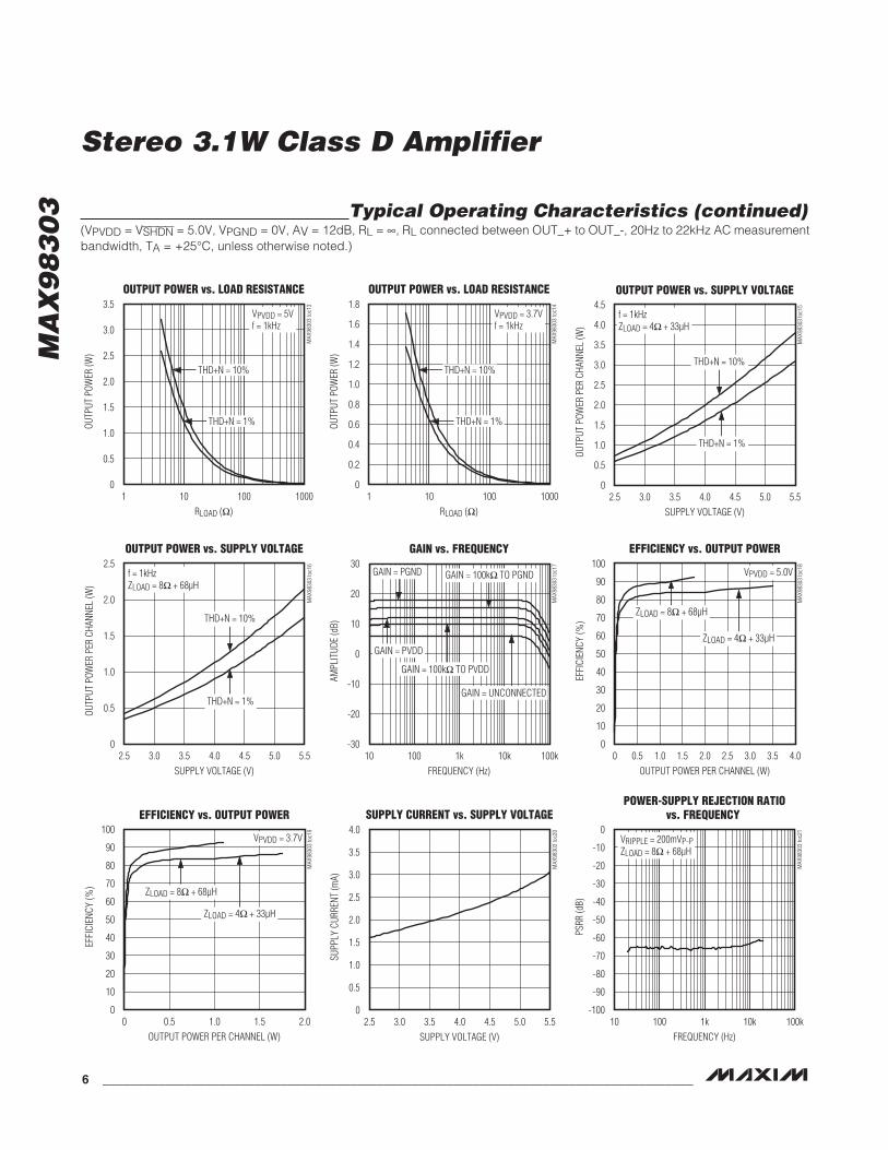
Typical Operating Characteristics(VPVDD = VSHDN = 5.0V, VPGND = 0V, AV = 12dB, RL = J, RL connected between OUT_+ to OUT_-, 20Hz to 22kHz AC measurement bandwidth, TA = +25NC, unless otherwise noted.)
ELECTRICAL CHARACTERISTICS (continued)(VPVDD = VSHDN = 3.7V, VPGND = 0V, AV = 12dB (GAIN = PVDD), RL = J, RL connected between OUT_+ to OUT_-, 20Hz to 22kHz AC measurement bandwidth, TA = TMIN to TMAX, unless otherwise noted. Typical values are at TA = +25NC.) (Notes 2, 3)
Note 2: This device is 100% production tested at TA = +25NC. All temperature limits are guaranteed by design.Note 3: Testing performed with a resistive load in series with an inductor to simulate an actual speaker load. For RL = 4I,
L = 33FH. For RL = 8I, L = 68FH.Note 4: Amplifier inputs AC-coupled to ground.Note 5: Mode transitions controlled by SHDN.
TOTAL HARMONIC DISTORTIONPLUS NOISE vs. FREQUENCY
MAX
9830
3 to
c01
FREQUENCY (Hz)
THD+
N (%
)
10k1k100
0.1
1
10
0.0110 100k
VPVDD = 5VZLOAD = 4I + 33µH
POUT = 2W
POUT = 1.5W
TOTAL HARMONIC DISTORTIONPLUS NOISE vs. FREQUENCY
MAX
9830
3 to
c02
FREQUENCY (Hz)
THD+
N (%
)
10k1k100
0.1
1
10
0.0110 100k
VPVDD = 4.2VZLOAD = 4I + 33µH
POUT = 0.2W
POUT = 1W
TOTAL HARMONIC DISTORTIONPLUS NOISE vs. FREQUENCY
MAX
9830
3 to
c03
FREQUENCY (Hz)
THD+
N (%
)
10k1k100
0.1
1
10
0.0110 100k
VPVDD = 3.7VZLOAD = 4I + 33µH
POUT = 0.8W
POUT = 0.2W
PARAMETER SYMBOL CONDITIONS MIN TYP MAX UNITS
Output Current Limit ILIM 2 A
Thermal Shutdown Level 145 NC
Thermal Shutdown Hysteresis 15 NC
DIGITAL INPUT (SHDN)Input Voltage High VINH VPVDD = 2.5V to 5.5V 1.4 V
Input Voltage Low VINL VPVDD = 2.5V to 5.5V 0.4 V
Input Leakage Current TA = +25NC ±1 FA

_______________________________________________________________________________________ 5
MA
X9
83
03
Stereo 3.1W Class D Amplifier
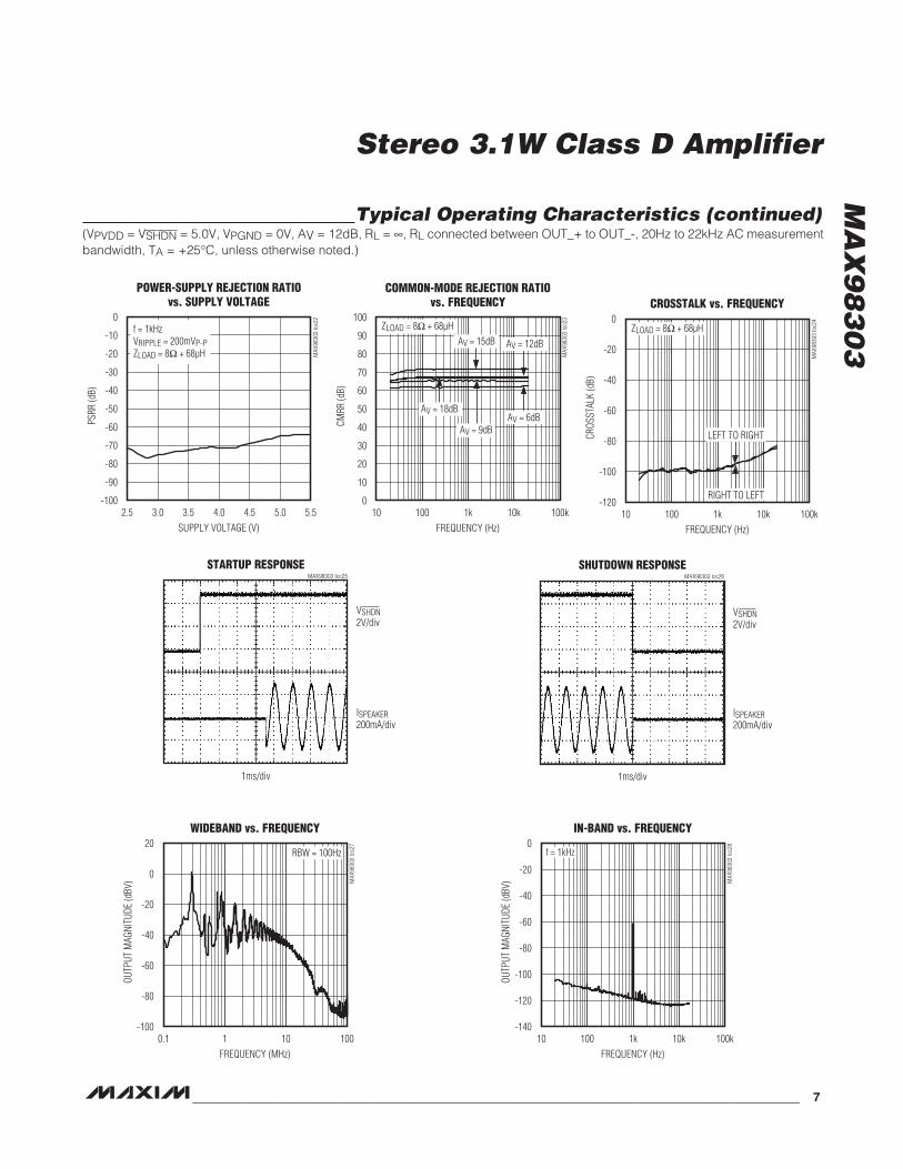
Typical Operating Characteristics (continued)(VPVDD = VSHDN = 5.0V, VPGND = 0V, AV = 12dB, RL = J, RL connected between OUT_+ to OUT_-, 20Hz to 22kHz AC measurement bandwidth, TA = +25NC, unless otherwise noted.)
TOTAL HARMONIC DISTORTIONPLUS NOISE vs. FREQUENCY
MAX
9830
3 to
c04
FREQUENCY (Hz)
THD+
N (%
)
10k1k100
0.1
1
10
0.0110 100k
VPVDD = 5VZLOAD = 8I + 68µH
POUT = 1.2W
POUT = 0.2W
TOTAL HARMONIC DISTORTIONPLUS NOISE vs. FREQUENCY
MAX
9830
3 to
c05
FREQUENCY (Hz)
THD+
N (%
)
10k1k100
0.1
1
10
0.0110 100k
VPVDD = 4.2VZLOAD = 8I + 68µH
POUT = 0.2W
POUT = 0.6W
TOTAL HARMONIC DISTORTIONPLUS NOISE vs. FREQUENCY
MAX
9830
3 to
c06
FREQUENCY (Hz)
THD+
N (%
)
10k1k100
0.1
1
10
0.0110 100k
VPVDD = 3.7VZLOAD = 8I + 68µH
POUT = 0.2W
POUT = 0.4W
TOTAL HARMONIC DISTORTIONPLUS NOISE vs. OUTPUT POWER
MAX
9830
3 to
c07
OUTPUT POWER (W)
THD+
N (%
)
3.02.52.01.51.00.5
0.1
1
10
100
0.010 3.5
VPVDD = 5VZLOAD = 4I + 33µH
f = 6000Hz
f = 1000Hz
f = 100Hz
TOTAL HARMONIC DISTORTIONPLUS NOISE vs. OUTPUT POWER
MAX
9830
3 to
c08
OUTPUT POWER (W)
THD+
N (%
)
2.01.51.00.5
0.1
1
10
100
0.010 2.5
VPVDD = 4.2VZLOAD = 4I + 33µH
f = 6000Hz
f = 1000Hz
f = 100Hz
TOTAL HARMONIC DISTORTIONPLUS NOISE vs. OUTPUT POWER
MAX
9830
3 to
c09
OUTPUT POWER (W)
THD+
N (%
)
1.51.00.5
0.1
1
10
100
0.010 2.0
VPVDD = 3.7VZLOAD = 4I + 33µH
f = 6000Hz
f = 1000Hz
f = 100Hz
TOTAL HARMONIC DISTORTIONPLUS NOISE vs. OUTPUT POWER
MAX
9830
3 to
c10
OUTPUT POWER (W)
THD+
N (%
)
1.51.00.5
0.1
1
10
100
0.010 2.0
VPVDD = 5VZLOAD = 8I + 68µH
f = 6000Hz
f = 1000Hz
f = 100Hz
TOTAL HARMONIC DISTORTIONPLUS NOISE vs. OUTPUT POWER
MAX
9830
3 to
c11
OUTPUT POWER (W)
THD+
N (%
)
1.20.90.60.3
0.1
1
10
100
0.010 1.5
VPVDD = 4.2VZLOAD = 8I + 68µH
f = 6000Hz
f = 1000Hz
f = 100Hz
TOTAL HARMONIC DISTORTIONPLUS NOISE vs. OUTPUT POWER
MAX
9830
3 to
c12
OUTPUT POWER (W)
THD+
N (%
)
1.00.80.60.40.2
0.1
1
10
100
0.010 1.2
VPVDD = 3.7VZLOAD = 8I + 68µH
f = 6000Hz
f = 1000Hz
f = 100Hz
6 ______________________________________________________________________________________
MA
X9
83
03
Stereo 3.1W Class D Amplifier
Typical Operating Characteristics (continued)(VPVDD = VSHDN = 5.0V, VPGND = 0V, AV = 12dB, RL = J, RL connected between OUT_+ to OUT_-, 20Hz to 22kHz AC measurement bandwidth, TA = +25NC, unless otherwise noted.)
OUTPUT POWER vs. LOAD RESISTANCEM
AX98
303
toc1
3
RLOAD (I)
OUTP
UT P
OWER
(W)
10010
0.5
1.0
1.5
2.0
2.5
3.0
3.5
01 1000
VPVDD = 5Vf = 1kHz
THD+N = 10%
THD+N = 1%
OUTPUT POWER vs. LOAD RESISTANCE
MAX
9830
3 to
c14
RLOAD (I)
OUTP
UT P
OWER
(W)
10010
0.2
0.4
0.6
0.8
1.0
1.2
1.4
1.6
1.8
01 1000
THD+N = 10%
THD+N = 1%
VPVDD = 3.7Vf = 1kHz
OUTPUT POWER vs. SUPPLY VOLTAGE
MAX
9830
3 to
c15
SUPPLY VOLTAGE (V)
OUTP
UT P
OWER
PER
CHA
NNEL
(W)
5.04.54.03.53.0
0.5
1.0
1.5
2.0
2.5
3.0
3.5
4.0
4.5
02.5 5.5
f = 1kHzZLOAD = 4I + 33µH
THD+N = 1%
THD+N = 10%
5.04.54.03.53.02.5 5.5
OUTPUT POWER vs. SUPPLY VOLTAGE
MAX
9830
3 to
c16
SUPPLY VOLTAGE (V)
OUTP
UT P
OWER
PER
CHA
NNEL
(W)
0.5
1.0
1.5
2.0
2.5
0
f = 1kHzZLOAD = 8I + 68µH
THD+N = 1%
THD+N = 10%
GAIN vs. FREQUENCYM
AX98
303
toc1
7
FREQUENCY (Hz)
AMPL
ITUD
E (d
B)
10k1k100
-20
-10
0
10
20
30
-3010 100k
GAIN = PGND GAIN = 100kI TO PGND
GAIN = PVDD
GAIN = 100kI TO PVDD
GAIN = UNCONNECTED
EFFICIENCY vs. OUTPUT POWER
MAX
9830
3 to
c18
OUTPUT POWER PER CHANNEL (W)
EFFI
CIEN
CY (%
)
3.53.02.0 2.51.0 1.50.50 4.0
10
20
30
40
50
60
70
80
90
100
0
ZLOAD = 8I + 68µH
ZLOAD = 4I + 33µH
VPVDD = 5.0V
EFFICIENCY vs. OUTPUT POWER
MAX
9830
3 to
c19
OUTPUT POWER PER CHANNEL (W)
EFFI
CIEN
CY (%
)
1.51.00.5
10
20
30
40
50
60
70
80
90
100
00 2.0
ZLOAD = 8I + 68µH
ZLOAD = 4I + 33µH
VPVDD = 3.7V
SUPPLY CURRENT vs. SUPPLY VOLTAGE
MAX
9830
3 to
c20
SUPPLY VOLTAGE (V)
SUPP
LY C
URRE
NT (m
A)
5.04.53.0 3.5 4.0
0.5
1.0
1.5
2.0
2.5
3.0
3.5
4.0
02.5 5.5
POWER-SUPPLY REJECTION RATIOvs. FREQUENCY
MAX
9830
3 to
c21
FREQUENCY (Hz)
PSRR
(dB)
10k1k10010 100k
-90
-80
-70
-60
-50
-40
-30
-20
-10
0
-100
VRIPPLE = 200mVP-PZLOAD = 8I + 68µH
_______________________________________________________________________________________ 7
MA
X9
83
03
Stereo 3.1W Class D Amplifier
Typical Operating Characteristics (continued)(VPVDD = VSHDN = 5.0V, VPGND = 0V, AV = 12dB, RL = J, RL connected between OUT_+ to OUT_-, 20Hz to 22kHz AC measurement bandwidth, TA = +25NC, unless otherwise noted.)
POWER-SUPPLY REJECTION RATIOvs. SUPPLY VOLTAGE
MAX
9830
3 to
c22
SUPPLY VOLTAGE (V)
PSRR
(dB)
5.04.54.03.53.0
-90
-80
-70
-60
-50
-40
-30
-20
-10
0
-1002.5 5.5
f = 1kHzVRIPPLE = 200mVP-PZLOAD = 8I + 68µH
COMMON-MODE REJECTION RATIOvs. FREQUENCY
MAX
9830
3 to
c23
FREQUENCY (Hz)
CMRR
(dB)
10k1k100
10
20
30
40
50
60
70
80
90
100
010 100k
ZLOAD = 8I + 68µH
AV = 12dBAV = 15dB
AV = 18dB
AV = 9dBAV = 6dB
CROSSTALK vs. FREQUENCY
MAX
9830
3 to
c24
FREQUENCY (Hz)
CROS
STAL
K (d
B)
10k1k100
-100
-80
-60
-40
-20
0
-12010 100k
ZLOAD = 8I + 68µH
RIGHT TO LEFT
LEFT TO RIGHT
STARTUP RESPONSEMAX98303 toc25
ISPEAKER200mA/div
VSHDN2V/div
1ms/div
SHUTDOWN RESPONSEMAX98303 toc26
ISPEAKER200mA/div
1ms/div
VSHDN2V/div
WIDEBAND vs. FREQUENCY
MAX
9830
3 to
c27
FREQUENCY (MHz)
OUTP
UT M
AGNI
TUDE
(dBV
)
101
-80
-60
-40
-20
0
20
-1000.1 100
RBW = 100Hz
IN-BAND vs. FREQUENCY
MAX
9830
3 to
c28
FREQUENCY (Hz)
OUTP
UT M
AGNI
TUDE
(dBV
)
10k1k100
-120
-100
-80
-60
-40
-20
0
-14010 100k
f = 1kHz
8 ______________________________________________________________________________________
MA
X9
83
03
Stereo 3.1W Class D Amplifier
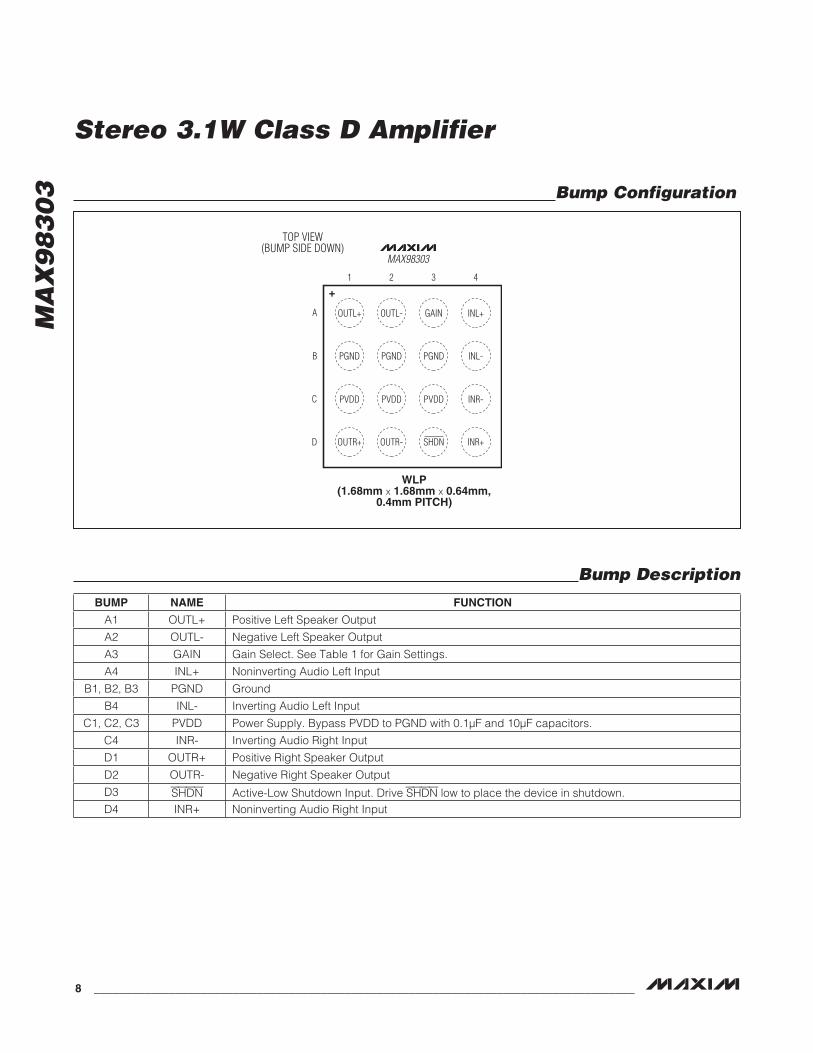
Bump Description
Bump Configuration
WLP(1.68mm O 1.68mm O 0.64mm,
0.4mm PITCH)
TOP VIEW(BUMP SIDE DOWN)
MAX98303
+
OUTL+
1
A
B
C
D
2 3 4
OUTL- GAIN INL+
PGND PGND PGND INL-
PVDD PVDD PVDD INR-
OUTR+ OUTR- SHDN INR+
BUMP NAME FUNCTION
A1 OUTL+ Positive Left Speaker Output
A2 OUTL- Negative Left Speaker Output
A3 GAIN Gain Select. See Table 1 for Gain Settings.
A4 INL+ Noninverting Audio Left Input
B1, B2, B3 PGND Ground
B4 INL- Inverting Audio Left Input
C1, C2, C3 PVDD Power Supply. Bypass PVDD to PGND with 0.1FF and 10FF capacitors.
C4 INR- Inverting Audio Right Input
D1 OUTR+ Positive Right Speaker Output
D2 OUTR- Negative Right Speaker Output
D3 SHDN Active-Low Shutdown Input. Drive SHDN low to place the device in shutdown.D4 INR+ Noninverting Audio Right Input

_______________________________________________________________________________________ 9
MA
X9
83
03
Stereo 3.1W Class D Amplifier
Detailed DescriptionThe MAX98303 features low quiescent current, a low-power shutdown mode, comprehensive click-and-pop suppression, and excellent RF immunity.
The IC offers Class AB audio performance with Class D efficiency in a minimal board-space solution.
The Class D amplifier features spread-spectrum modu-lation, edge-rate, and overshoot control circuitry that offers significant improvements to switch-mode amplifier radiated emissions.
The amplifier features click-and-pop suppression that reduces audible transients on startup and shutdown. The amplifier includes thermal-overload and short-circuit protection.
Class D Speaker AmplifierThe filterless Class D amplifier offers much higher effi-ciency than Class AB amplifiers. The high efficiency of a Class D amplifier is due to the switching operation of the output stage transistors. Any power loss associated with the Class D output stage is mostly due to the I2R loss of the MOSFET on-resistance and quiescent current overhead.
Ultra-Low-EMI Filterless Output StageTraditional Class D amplifiers require the use of external LC filters, or shielding, to meet EN55022B electromagnet-ic-interference (EMI) regulation standards. Maxim’s active emissions limiting edge-rate control circuitry and spread-spectrum modulation reduce EMI emissions, while main-taining up to 93% efficiency.
Maxim’s spread-spectrum modulation mode flattens wideband spectral components, while proprietary tech-niques ensure that the cycle-to-cycle variation of the switching period does not degrade audio reproduction or efficiency. The IC’s spread-spectrum modulator ran-domly varies the switching frequency by Q15kHz around the center frequency (300kHz). Above 10MHz, the wideband spectrum looks like noise for EMI purposes (Figure 1).
Speaker Current LimitIf the output current of the speaker amplifier exceeds the current limit (2A typ), the IC disables the outputs for approximately 100Fs. At the end of 100Fs, the outputs are reenabled. If the fault condition still exists, the IC continues to disable and reenable the outputs until the fault condition is removed.
Selectable GainThe IC offers five programmable gains selected using the GAIN input.
ShutdownThe IC features a low-power shutdown mode, drawing P 0.1FA (typ) of supply current. Drive SHDN low to place the MAX98303 into shutdown.
Click-and-Pop SuppressionThe IC speaker amplifier features Maxim’s comprehen-sive click-and-pop suppression. During startup, the click-and-pop suppression circuitry reduces any audible transient sources internal to the device. When entering shutdown, the differential speaker outputs ramp down to PGND quickly and simultaneously.
Table 1. Gain Control Configuration
Figure 1. EMI with 30cm of Speaker Cable and No Output Filter
GAIN PIN MAXIMUM GAIN (dB)
Connect to PGND 18
Connect to PGND through 100kI ±5% resistor
15
Connect to PVDD 12
Connect to PVDD through 100kI ±5% resistor
9
Unconnected 6
90
70
50
30
10
-100 100 200 300 400 500 600 700 800 900 1000
EMIS
SION
S LE
VEL
(dBµ
V/m
)
FREQUENCY (MHz)
EN55022B LIMIT
HORIZONTAL
VERTICAL

10 _____________________________________________________________________________________
MA
X9
83
03
Stereo 3.1W Class D Amplifier
Applications InformationFilterless Class D Operation
Traditional Class D amplifiers require an output filter. The filter adds cost and size and decreases THD perfor-mance. The IC’s filterless modulation scheme does not require an output filter.
Because the switching frequency of the IC is well beyond the bandwidth of most speakers, voice coil movement due to the switching frequency is very small. Use a speaker with a series inductance > 10FH. Typical 8I speakers exhibit series inductances in the 20FH to 100FH range.
Component SelectionPower-Supply Input (PVDD)
PVDD powers the speaker amplifier. PVDD ranges from 2.6V to 5.5V. Bypass PVDD with 0.1FF and 10FF capaci-tors to PGND. Apply additional bulk capacitance at the device if long input traces between PVDD and the power source are used.
Input FilteringThe input-coupling capacitor (CIN), in conjunction with the amplifier’s internal input resistance (RIN), forms a highpass filter that removes the DC bias from the incom-ing signal. These capacitors allow the amplifier to bias the signal to an optimum DC level.
Assuming zero source impedance with a gain setting of 12dB, 15dB, or 18dB, CIN is:
IN3dB
8C [ F]
f−= µ
with a gain setting of 9dB, CIN is:
IN3dB
5.7C [ F]
f−= µ
with a gain setting of 6dB, CIN is:
IN3dB
4C [ F]
f−= µ
where f-3dB is the -3dB corner frequency. Use capaci-tors with adequately low-voltage coefficients for best low-frequency THD performance.
Layout and GroundingProper layout and grounding are essential for optimum performance. Good grounding improves audio perfor-mance and prevents switching noise from coupling into the audio signal.
Use wide, low-resistance output traces. As the load impedance decreases, the current drawn from the device increases. At higher current, the resistance of the output traces decrease the power delivered to the load. For example, if 2W is delivered from the device output to a 4I load through 100mI of total speaker trace, 1.904W is delivered to the speaker. If power is delivered through 10mI of total speaker trace, 1.99W is delivered to the speaker. Wide output, supply, and ground traces also improve the power dissipation of the device.
The IC is inherently designed for excellent RF immunity. For best performance, add ground fills around all signal traces on top or bottom PCB planes.
WLP Applications InformationFor the latest application details on WLP construction, dimensions, tape carrier information, PCB techniques, bump-pad layout, and recommended reflow tempera-ture profile, as well as the latest information on reliability testing results, refer to Application Note 1891: Wafer level packaging (WLP) and its applications. Figure 2 shows the dimensions of the WLP balls used on the IC.
Figure 2. MAX98303 WLP Ball Dimensions
0.24mm
0.21mm

______________________________________________________________________________________ 11
MA
X9
83
03
Stereo 3.1W Class D Amplifier
Chip InformationPROCESS: CMOS
Block Diagram
CLASS D MODULATOR
A4INL+
A1
OUTL+
OUTL-A2
PVDD
D3
0.1µF
PVDD
C1, C2, C3
SHDN
INL-
GAIN
B4
A3
UVLO/POWERMANAGEMENT
CLICK-AND-POPSUPPRESSION
2.6V TO 5.5V
LOW-EMIDRIVER
PVDD
PGND
LOW-EMIDRIVER
PVDD
PGND
PGND
B1, B2, B3
MAX98303
10µF
CLASS D MODULATOR
D4INR+
D1
OUTR+
OUTR-D2
INR- C4
LOW-EMIDRIVER
PGND
LOW-EMIDRIVER
PVDD
PVDD
PGND
PVDD

12 _____________________________________________________________________________________
MA
X9
83
03
Stereo 3.1W Class D Amplifier
Package InformationFor the latest package outline information and land patterns, go to www.maxim-ic.com/packages. Note that a “+”, “#”, or “-” in the package code indicates RoHS status only. Package drawings may show a different suffix character, but the drawing pertains to the package regardless of RoHS status.
PACKAGE TYPE PACKAGE CODE OUTLINE NO. LAND PATTERN NO.
16 WLP W161B1+1 21-0491 —
Maxim cannot assume responsibility for use of any circuitry other than circuitry entirely embodied in a Maxim product. No circuit patent licenses are implied. Maxim reserves the right to change the circuitry and specifications without notice at any time.
Maxim Integrated Products, 120 San Gabriel Drive, Sunnyvale, CA 94086 408-737-7600 13
© 2010 Maxim Integrated Products Maxim is a registered trademark of Maxim Integrated Products, Inc.
MA
X9
83
03
Stereo 3.1W Class D Amplifier
Revision History
REVISIONNUMBER
REVISION DATE
DESCRIPTIONPAGES
CHANGED
0 9/10 Initial release —