superemission in vertically-aligned single-wall carbon
TRANSCRIPT

A
simdadtWaSttaP
K
1
cciT
f
1
Photonics and Nanostructures – Fundamentals and Applications 21 (2016) 67–81
Available online at www.sciencedirect.com
ScienceDirect
Superemission in vertically-aligned single-wall carbon nanotubes
Igor Khmelinskii a, Vladimir Makarov b,∗a University of the Algarve, FCT, DQB and CIQA, 8005-139 Faro, Portugal
b University of Puerto Rico, Rio Piedras Campus, PO Box 23343, San Juan, PR 00931-3343, USA
Received 4 April 2016; received in revised form 17 July 2016; accepted 18 July 2016Available online 25 July 2016
bstract
Presently we used two samples of vertically aligned single-wall carbon nanotubes (VA SWCNTs) with parallelepiped geometry,ized 0.02 cm × 0.2 cm × 1.0 cm and 0.2 cm × 0.2 cm × 1.0 cm. We report absorption and emission properties of the VA SWCNTs,ncluding strong anisotropy in both their absorption and emission spectra. We found that the emission spectra extend from the
iddle-IR range to the near-IR range, with such extended spectra being reported for the first time. Pumping the VA SWCNTs in theirection normal to their axis, superemission (SE) was observed in the direction along their axis. The SE band maximum is locatedt 7206 ± 0.4 cm−1. The energy and the power density of the superemission were estimated, along with the diffraction-limitedivergence. At the pumping energy of 3 mJ/pulse, the SE energy measured by the detector was 0.74 mJ/pulse, corresponding to theotal SE energy of 1.48 mJ/pulse, with the energy density of 18.5 mJ cm−2/pulse and the SE power density of 1.2 × 10⁵ W cm−2/pulse.
e report that a bundle of VA SWCNTs is an emitter with a relatively small divergence, not exceeding 3.9 × 10⁻³ rad. We developed theoretical approach to explain such absorption and emission spectra. The developed theory is based on the earlier proposedSH theory, which we extended to include the exchange interactions between the closest SWCNT neighbors. The developed
heoretical ideas were implemented in a homemade FORTRAN code. This code was successfully used to calculate and reproduce
he experimental spectra and to determine the SWCNT species that originate the respective absorption bands, with acceptablegreement between theory and experiment.ublished by Elsevier B.V.Electro
eywords: A Nanostructures; B Composites; C Optical properties; D. Introduction
Many earlier studies were devoted to the unique opti-al properties of carbon nanotubes [1–3]. Single-walled
arbon nanotubes (SWCNTs) are a special and verynteresting material, as regards their optical properties.heir diameter is typically in the 1.0–5.0 nm range, with∗ Corresponding author. Tel.: +1 787 529 2010;ax: +1 787 764 7717.
E-mail address: [email protected] (V. Makarov).
�
http://dx.doi.org/10.1016/j.photonics.2016.07.003569-4410/Published by Elsevier B.V.
n microscopy; D Electronic structure
the tube length significantly exceeding its diameter. Thestructure of a SWCNT may be characterized by a pairof integer numbers (n,m), which define the vector of thesystem translational symmetry:
r = m�a1 + n�a2 (1)
where a1 and a2 are the primitive vectors of the graphenelattice cell. The nanotubes have a zigzag structure when

uctures
68 I. Khmelinskii, V. Makarov / Photonics and Nanostrm = 0, and an armchair structure when n = m. The diam-eter of an ideal nanotube may be calculated as follows:
d = a
π
√(m + n)2 − mn (2)
where a = 0.246 nm.The SWCNT properties change significantly in func-
tion of the (n,m) values, in a non-monotonous manner[3]. For example, the band gap in the SWCNTs variesfrom zero to about 2 eV, with their electric conductiv-ity showing either metallic or semiconducting behavior.These fundamental properties very strongly affect theiroptical properties.
The density of states (DOS) in semiconducting carbonnanotubes is independent of the translational unit cellsize and the chiral angle [3–6]. The absorption spectraand the electron energy loss spectra (EELS) of SWCNTbundles were calculated, with the energies of the threemain peaks given approximately by [3–6]:
El = 2la
d
∣∣Vppπ∣∣ , l = 1, 2, 3 (3)
where Vppπ is the ppπ transfer integral between the twonearest carbon atoms. The p orbital rehybridization effecton the peak position was extensively studied as well[7–10]. It was found that such rehybridization may sig-nificantly change the DOS of the SWCNTs. Chen et al.[11] took these effects into account in their calcula-tions, obtaining a good agreement between theoreticaland experimental spectra. A theoretical analysis of thedetailed structure of the SWCNT absorption bands wascarried by Prylutsky et al. [12]. They found that spe-cific groups of subbands appear in different parts ofthe SWCNT absorption spectrum, with the resultingspectrum significantly more complex than the spec-tra than only have three principal absorption bands.Therefore, it is very important to discuss the experimen-tal measurements of the SWCNT absorption spectra.Meyyappan [13] described the absorption spectra ofthe high purity metallic and semiconducting SWCNTs,separated using the density-gradient ultracentrifugation.The spectra were recorded in the wide energy rangefrom 1 meV to 5 eV. A strong and broad absorptionband was observed at 0.06 eV in a high-purity metal-lic nanotube sample. This observation suggests thatthe optical properties of even the high-purity metallicnanotube bundles cannot be described by the simpleDrude conduction model. The origin of these absorp-
tion bands for the metallic and semiconducting nanotubesamples was discussed [14], taking into account thesmall energy gap in the metallic nanotube bundles andplasmonic resonance. Leson et al. [15] carried out an– Fundamentals and Applications 21 (2016) 67–81
experimental investigation of the optical spectra of theSWCNTs at temperatures up to 1273 K. Their studiesgive insights into the electronic structure of the metallicand semiconducting SWCNTs at different temperaturesby measuring the shifts of the S11, S22 and M11 bandsusing optical absorption spectroscopy, where S refersto the semiconducting SWCNTs and M to the metallicSWCNTs.
A decrease in the transition energies in both metal-lic and semiconducting SWCNTs with temperature isdetermined by the temperature shift of the S11, S22and M11 absorption bands. Weisman et al. [16] ana-lyzed the absorption spectra of the SWCNTs scannedover a wide spectral range. The broad backgrounds inthe visible-near-IR absorption spectra were studied in aseries of tightly controlled experiments [16], reportingno major differences between the spectral backgroundsin the sample fractions with the average lengths between120 and 650 nm. Thus, the authors concluded that thebroad background absorption is created by an amorphouscarbon fraction present in the SWCNT samples [16].Takeyama et al. [17] performed measurements of theoptical absorption cross-section of the SWCNTs. Theyprovided an empirical formula allowing to predict theabsorption spectrum of any SWCNT. A detailed analysisof the above reports shows that the SWCNTs demon-strate very interesting optical properties, which justifyan additional research effort. Lately we demonstrated[18] that metal nanolayers produce superemission; wetherefore expected to obtain similar effects in SWCNTsas well.
Single-walled carbon nanotubes are a very promisingmaterial for broad technological applications [19,20].The diameters of SWCNTs vary in the range of 1–5 nmand the length exceeds the diameter by the factor of102–107. Ugawa et al. [21] studied the MIR energygap in the SWCNTs. They found that the energy gapof metal-like SWCNTs is about several thousand cm−1.Thus, the lowest-energy transitions in the absorption andemission spectra should be located in the MIR spectralregion. The electronic structure of the SWCNTs was alsostudied quite extensively using optical spectroscopy andab initio calculations [22–24]. The perturbations in thecommon conjugated �-system were found to increasedramatically for thinner SWCNTs. The optical absorp-tion and emission, and the excited state dynamics ofSWCNTs were also investigated in detail [25–47], withthe emission spectrum of the individual SWCNTs typ-
ically appearing in the NIR range, and the dynamicsdeveloping in the subpicosecond time range. However,the radiative lifetime of the relaxed system is typicallyin the nanosecond time range.
uctures – Fundamentals and Applications 21 (2016) 67–81 69
wcSdu
ctnStastsmScsst
2
2
efSpftfTnt6dttsSerab
Sr
the light source (ESI 1200 100W MSR Lamp 3.8 A;Planet Bulb Inc.), the radiation was focused by appro-priate lenses, filtered by a water-cooled glass filter to
I. Khmelinskii, V. Makarov / Photonics and Nanostr
The optical properties of different SWCNT isomersere also studied [48], with the differences in opti-
al properties of different isomers of single-chiralityWCNTs used to separate these isomers. A method toetermine the SWCNT diameter was also proposed andsed to characterize the SWCNT morphology [49].
Presently, we report experimental and theoreticallyalculated absorption and emission spectra of the ver-ically aligned (VA) semiconductor SWCNTs (m /= 0,
/= 0). Both absorption and emission spectra of the VAWCNTs demonstrate very strong anisotropy as regards
he locations of the peak maxima and the peak widths. Welso found that VA SWCNTs produce strong superemis-ion in the direction of the tube axis. We also report that inhe macroscopic bundle of the VA SWCNTs the emissionpectra appear in the near-IR spectral range, in agree-ent with the NIR-only emission obtained for individualWCNTs. We describe the observed absorption spectraonsidering the cooperative effects in this macroscopicystem. Thus, we report the absorption, emission anduperemission spectra of the VA SWCNTs, and proposeheoretical models explaining the experimental results.
. Experimental methods
.1. Samples
The experimental measurements of the absorption,mission and superemission spectra were performedor samples consisting of bundles of vertically-alignedWCNTs with 0.02 cm × 0.2 cm × 1.0 cm size (sam-le T1) and 0.2 cm × 0.2 cm × 1.0 cm size (sample T2)rom Firstnano (www.firstnano.com), with the nano-ube length of 1.0 cm, grown in the central zone of theused silica substrates (1.25 cm × 1.25 cm × 0.05 cm).he average SWCNT diameter was 3.7 nm, and theirumber density ca. 1.7 × 10⁵ �m−2. The upper ends ofhe SWCNTs were trimmed to the same length using00 eV Cs ion beam, with the upper surface of the bun-le parallel to the substrate. Thus, the lengths of all ofhe SWCNTs were essentially equal. The substrates withhe SWCNT bundles were mounted on a support, with aecond fused silica plate protecting the upper ends of theWCNTs from damage, mounted with a spacing of sev-ral �m (see Fig. 1). The spectra of the samples could beecorded using different geometries. The emission waslways captured in the direction normal to the excitation
eam.To characterize the samples, we recorded theEM image of the T1 sample (JSM-7800F Extreme-esolution Analytical Field Emission SEM, Jeol Inc.).
Fig. 1. The sample geometry: (A, B) the lateral faces of the verticallyaligned SWCNT bundle; (C) the upper face of the vertically alignedSWCNT bundle; (D) the fused silica substrate.
The 0.2 cm × 1.0 cm sample face was scanned, with theSEM image shown in Fig. 2.
The SEM image shows well-aligned SWCNTs, withthe average diameter as estimated from the image being4.3 ± 1.8 nm, in acceptable agreement with the producerspecifications.
2.2. The experimental methods and techniques
The absorption and emission spectra were recordedon a Hitachi U-3900H UV-Visible and Shimadzu UV-3600 Plus Spectrophotometers, and FTIR spectrometer(IFS 66/S, Bruker Inc., with LN2 cooled detectors),respectively. The spectral peak maxima and widths werecalculated using the PeakFit software (Sigmaplot). Thesamples were reproducibly installed into a support ofblackened aluminum.
Fig. 3 shows the block diagram of the experimentalsetup used for measurements of the superemission spec-tra. A high-pressure 100W mercury lamp was used as
Fig. 2. The SEM image of the T1 sample, showing a bundle ofvertically-aligned single-walled carbon nanotubes.

70 I. Khmelinskii, V. Makarov / Photonics and Nanostructures
1
3
2
44
5
6
77
8
8
9 10
11
1213
4 4’
3 3’
Fig. 3. Superemission measurements: 1, the face of the SWCNT sam-ple; 2, the substrate; 3, 10 cm focal distance cylindrical lens (viewedfrom the top); 3′, the same, viewed from the left side; 4, 30 cm cylin-drical lens (viewed from the top); 4′, the same, viewed from the leftside; 5, 6, 7, the excitation laser beam focused on the sample face; 8,superemission exiting the top face of the sample; 9, condenser lens;
lic SWCNTs. Later on we shall simulate the absorption
10, spherical lens (5 mm or 30 cm focal distance); 11, sample emissionpassing through 9 and 10; 12, monocromator; 13, PD1 detector.
separate the 313 nm Hg emission band, and focused intoa 0.2 cm × 0.1 cm spot at the sample location, using anappropriate slit. The IR-NIR superemission was col-lected by a CaF2 lens onto the entrance slit of themonochromator (Cornerstone 130 1/8m Monochroma-tors, NewPort Inc.), and detected by a photodiode (PD1;DET10A Si biased detector, THORLABS). The outputof the PD1 signal was digitized by PCI-6034E DAQ I/Oboard (National Instruments), with the control code inthe LABVIEW environment running on a Dell PC. TheNIR and middle IR emission was focused onto the inputslit of the FTIR spectrometer, the spectra were scannedand the data collected by a PC computer.
For superemission measurements, an additionalexperimental setup was used. An additional excitationsource used a frequency-doubled (BBO crystal) dyelaser (LPD-2000, �-Physics, with Pyrromethene-556dye, 540–580 nm range; frequency-doubled radiation at270–290 nm) pumped by a XeCl excimer laser (LPX-200, �-Physics).The laser pulse was about 15–20 nslong. The dye laser radiation was focused by a cylin-drical lens onto either A or B face of the sample (Fig. 1).
The superemission was collected by a 30-cm spheri-cal CaF2 lens and registered by a photodiode (PD1;DET10A Biased Si Detector from THORLABS), after– Fundamentals and Applications 21 (2016) 67–81
passing through a neutral density filter and a monochro-mator (Cornerstone 130 1/8 m Monochromator, NewPortInc.). The data acquisition system was controlled by a PCcomputer, using a digital oscilloscope (WaveSurfer 400from LeCroy), digital delay generators (DG-535, Stan-ford Research), boxcar integrators (SR-250, StanfordResearch), a fast amplifier (SR-240, Stanford Research),and a computer interface board (SR-245, StanfordResearch). The superemission spectra were scanned at1 cm−1 resolution. The superemission energy was mea-sured using a calibrated photodiode (DET10A Si biaseddetector, THORLABS). The presently developed exper-imental methods allowed recording the time evolutionand the spectra of the superemission with high accuracy,2.5 ns and 1.5 cm−1, respectively.
3. Experimental results
3.1. Absorption spectra
The absorption spectra were recorded, shown inFigs. 4–6.
Both T1 and T2 samples (Figs. 4 and 5) producedspectra composed of narrow discrete bands, with theaverage bandwidth of 112 ± 10 cm−1, and the band max-ima positions independent on the sample optical length.Additionally, two broad bands 3670 ± 130 cm−1 wideare visible in the thinner T1 sample. The relative inten-sities of the narrow bands are quite different in the twosamples. The band maxima and intensities (in the O.D.units) are listed in Table 1, calculated using the Peak-Fitpackage. Taking into account that the SWCNT densityis 1.7 × 1013 cm−3, their absorption cross section wasestimated using the Lambert-Beer law:
D = σnl, (4)
with D the optical density, σ the absorption cross-section,n the density of SWCNTs, and l the optical path length.The estimated values of the absorption cross-sectionsare also listed in Table 1. The ratio of the absorptioncross sections of the two samples is additionally shownin the last column. The intensity ratio that most dif-fers from unity is the one obtained for the 22896 cm−1
band (number 3 in Table 1). The narrow spectral bandsmay be assigned to different (m,n) configurations of thesemiconducting SWCNTs, with the electronic transi-tions induced between discrete electronic states, whilethe continuum spectrum may be attributed to the metal-
spectra of different types of SWCNTs.The absorption spectrum of the T2 sample measured
along the VA SWCNT axis direction is shown in Fig. 6.

I. Khmelinskii, V. Makarov / Photonics and Nanostructures – Fundamentals and Applications 21 (2016) 67–81 71
F t spectrt cm sam
TFvobstω
sreivapa
3
Trtf
ig. 4. The absorption spectra of the T1 sample, presented in differenhe SWCNT axis; the spectrum was recorded through the 0.2 cm × 1.0
his spectrum is completely different from those ofigs. 4 and 5. It has a broad transmission band in theisible and near UV, with a higher absorbance outsidef this window (curve 1 in Fig. 6). This transmissionand was represented by a superposition of two Gaussianubbands with the following maxima, widths and ampli-udes: ω1 = 25341 cm−1, γ1 = 5612 cm−1, A1 = 0.93;
2 = 35187 cm−1, γ2 = 5612 cm−1, A2 = 0.61. Thus, theample is transparent in the visible and near-UV spectralange. We interpret these two bands as the two differentlectronic transitions activated when the excitation lightn parallel to the nanotube axis, with the electric fieldector E normal to the same axis. Note the very strongnisotropy in the absorption spectra recorded for therobe beam directed normal and parallel to the nanotubexis, to be discussed later.
.1.1. Emission spectraThe emission spectra were studied for both the
1 and T2 samples, using the right-angles configu-ation, namely, the excitation was performed throughhe 0.2 × 1.0 cm2 faces, and the emission recordedrom the 0.02 cm × 1.0 cm and 0.02 cm × 0.2 cm faces
al ranges. The spectra were obtained with the probe beam normal tople faces with the 0.02 cm optical thickness.
for the T1 sample, and from the 0.2 cm × 1.0 cm and0.2 cm × 0.2 cm faces for the T2 sample. The excitationwas performed at 280 and 357 nm into the broad absorp-tion bands (see Fig. 4). Figs. 7 and 8 show the emissionspectra for the respective samples T1 and T2.
We see in Figs. 7 and 8 that the emission spectrumrecorded normal to the nanotube axis is quite broad,exhibiting a series of discrete bands, charts (a,1) and(b,1), while the spectrum recorded in the direction of thenanotube axis has a single narrow radiation band, charts(a,2) and (b,2). The respective band maxima, intensitiesand widths are listed in Table 2.
3.1.2. The superemissionSuperemission may be observed if we create a popula-
tion inversion between an excited state and a lower-lying(excited) state, when optical transitions between thesetwo states are allowed. A higher excited state may bepopulated directly by optical absorption, or indirectly
via relaxation from the initially created excited state toan intermediate state, lying above an unpopulated state.Provided the linear size of the active medium in onedirection (z) is much larger than that in the other two
72 I. Khmelinskii, V. Makarov / Photonics and Nanostructures – Fundamentals and Applications 21 (2016) 67–81
(a)
Energy (cm-1 )
10000 20000 30000 40000
Opt
ical
Den
sity
0.0
0.2
0.4
0.6
0.8
1.0
1.2
1.4
1.6
(b)
Energy (cm-1 )
10000 15000 20000 25000
Opt
ical
Den
sity
0.0
0.2
0.4
0.6
0.8
1.0
1.2
1.4
1.6
(d)
Energy (cm-1 )
7000 8000 9000 10000
Opt
ical
Den
sity
0.1
0.2
0.3
0.4
0.5
0.6
S(7,5)
(c)
Energy (cm-1)
8000 1000 0 1200 0 1400 0
Opt
ical
Den
sity
0.1
0.2
0.3
0.4
0.5
0.6
t spect cm sam
Fig. 5. The absorption spectra of the T2 sample, presented in differenthe SWCNT axis; the spectrum was recorded through the 0.2 cm × 1.0
directions (x,y), superemission will be observed in boththe −z and +z directions.
All of the measurements of the superemission werecarried out for the T1 sample, with the excitation beampassing through the 0.2 cm × 1.0 cm faces, and the emis-
1
Energy (cm-1)
0 10000 20000 30000 40000 50000
Opt
ical
Den
sity
0.0
0.2
0.4
0.6
0.8
1.0
1.2
3
2
Fig. 6. The absorption spectrum of the T2 sample: 1, the experimentalspectrum; 2, 3, the transmission band decomposed into two Gaussiansubbands. The spectrum was recorded with the probe beam parallelto the SWCNT axis, through the 0.2 cm × 0.2 cm sample faces with1.0 cm optical thickness.
ral ranges. The spectra were obtained with the probe beam normal tople faces with the 0.2 cm optical thickness.
sion recorded at the 0.02 cm × 0.2 cm face. Thus, theexcitation was performed normal to the nanotube axis,and the emission recorded in the direction of the axis.We recorded the laser-induced fluorescence excitationspectrum in the 270–290 nm range, using the frequency-doubled dye laser at 3.1 mJ/pulse, with the spectrumshown in Fig. 9.
Fig. 9 shows the laser induced fluorescence (LIF)spectrum recorded for the T1 sample excited normal tothe VA SWCNT axis. The total emission, including lightemitted in the near-IR, and UV–vis spectral ranges, wasdetected in the direction along the VA SWCNT axis. Thespectrum was fitted by a superposition of Gaussian andLorentzian functions:
ILIF = AGe−(ω−ω0/σG)2 + AL
1 +(ω−ω0σL
)2 (5)
−1
where AG = 73 ± 8; ω0 = 35781 ± 101 cm ; σG = σL =3302 ± 217 cm−1; AG = 61 ± 7. Zero-slope straight-linebackground was used in the fitting procedure. Thus,this band coincides with the band 1 of the absorption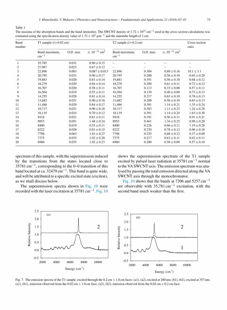
I. Khmelinskii, V. Makarov / Photonics and Nanostructures – Fundamentals and Applications 21 (2016) 67–81 73
Table 1The maxima of the absorption bands and the band intensities. The SWCNT density of 1.72 × 1013 cm−3 used in the cross-section calculations wasestimated using the specification density value of 1.72 × 10⁵ �m−2 and the nanotube length of 1 cm.
Bandnumber
T1 sample (l = 0.02 cm) T2 sample (l = 0.2 cm) Cross-sectionratio
Band maximum,cm−1
O.D. max σ, 10−11 cm2 Band maximum,cm−1
O.D. max σ, 10−11 cm2
1 35,785 0.031 0.90 ± 0.15 – – – –2 27,987 0.023 0.67 ± 0.12 – – – –3 22,896 0.003 0.087 ± 0.013 22,896 0.304 0.88 ± 0.16 10.1 ± 3.14 20,795 0.031 0.90 ± 0.17 20,795 0.200 0.58 ± 0.10 0.65 ± 0.205 19,883 0.028 0.81 ± 0.14 19,883 0.191 0.56 ± 0.10 0.68 ± 0.126 18,279 0.029 0.84 ± 0.14 18,279 0.209 0.61 ± 0.11 0.72 ± 0.127 16,707 0.020 0.58 ± 0.11 16,707 0.113 0.33 ± 0.08 0.57 ± 0.118 16,504 0.019 0.55 ± 0.11 16,504 0.139 0.40 ± 0.09 0.73 ± 0.139 14,255 0.028 0.81 ± 0.14 14,255 0.217 0.63 ± 0.10 0.78 ± 0.13
10 13,682 0.031 0.90 ± 0.18 13,682 0.200 0.58 ± 0.10 0.65 ± 0.1311 11,486 0.029 0.84 ± 0.17 11,486 0.391 1.14 ± 0.21 1.35 ± 0.2412 10,717 0.031 0.90 ± 0.18 10,717 0.383 1.11 ± 0.23 1.24 ± 0.2613 10,119 0.024 0.70 ± 0.12 10,119 0.391 1.14 ± 0.24 1.63 ± 0.3014 9418 0.021 0.61 ± 0.11 9418 0.191 0.56 ± 0.11 0.91 ± 0.2115 8953 0.051 1.48 ± 0.24 8953 0.461 1.34 ± 0.25 0.90 ± 0.2016 8400 0.019 0.55 ± 0.11 8400 0.226 0.66 ± 0.11 1.19 ± 0.2817 8222 0.028 0.81 ± 0.15 8222 0.270 0.78 ± 0.13 0.96 ± 0.1818 7798 0.063 1.83 ± 0.27 7798 0.235 0.68 ± 0.12 0.37 ± 0.091 73752 6960
sb3baa
r
F(
9 7375 0.035 1.02 ± 0.20
0 6960 0.035 1.02 ± 0.23
pectrum of this sample, with the superemission inducedy the transitions from the states located close to5781 cm−1, corresponding to the 0–0 transition of thisand located at ca. 32479 cm−1. This band is quite wide,nd will be attributed to a specific excited state (exciton),
s we shall discuss below.The superemission spectra shown in Fig. 10 wereecorded with the laser excitation at 35781 cm−1. Fig. 10
(a)
Energy (cm-1)
2000 4000 6000 8000 10000
Rel
ativ
e In
tens
ity
-0.5
0.0
0.5
1.0
1.5
2.0
2.5
1
2
ig. 7. The emission spectra of the T1 sample, excited through the 0.2 cm × 1.a1), (b1), emission observed from the 0.02 cm × 1.0 cm face; (a2), (b2), emis
0.217 0.63 ± 0.11 0.62 ± 0.11 0.200 0.58 ± 0.09 0.57 ± 0.10
shows the superemission spectrum of the T1 sampleexcited by pulsed laser radiation at 35781 cm−1 normalto the VA SWCNT axis. The emission spectrum was ana-lysed by passing the total emission directed along the VASWCNT axis through the monochromator.
Fig. 10 shows that the bands at 7206 and 5257 cm−1
are observable with 35,781 cm−1 excitation, with thesecond band much weaker than the first.
(b)
Energy (cm-1)
2000 4000 6000 8000 10000
Rel
ativ
e In
tens
ity
-0.5
0.0
0.5
1.0
1.5
2.0
2.5
1
2
0 cm faces: (a1), (a2), excited at 280 nm; (b1), (b2), excited at 357 nm;sion observed from the 0.02 cm × 0.2 cm face.

74 I. Khmelinskii, V. Makarov / Photonics and Nanostructures – Fundamentals and Applications 21 (2016) 67–81
(a)
-1
2000 400 0 600 0 800 0 1000 0
Rel
ativ
e In
tens
ity
-0.5
0.0
0.5
1.0
1.5
2.0
(b)
-1
2000 400 0 600 0 800 0 1000 0
Rel
ativ
e In
tens
ity
-0.5
0.0
0.5
1.0
1.5
2.0
2.5
1
2
1
2
× 1.0 c), emiss
Energy (cm )
Fig. 8. Emission spectra of the T2 sample, excited through the 0.2 cm(a1), (b1), emission observed from the 0.2 cm × 1.0 cm face; (a2), (b2
The SE kinetics was recorded for both bands usingthe 36,500 cm−1 excitation, with the waveforms shownin Fig. 11.
The first waveform was fitted by an exponential func-tion:
I(1)SE = A
(1)SEe
−t/τ(1)SE (6)
with τSE(1) = 152 ± 21 ns, while the second
waveform—by a sum of two exponentials:
I(2)SE = A
(2)SE
(e− t
τ(2,1)SE − e
− t
τ(2,2)SE
)(7)
Table 2The emission band maxima, intensities and widths (see the spectra in Figs. 7
a b c
ω, cm−1 A W, cm−1 ω, cm−1 A W, cm−1 ω
Fig. 71949 2 147 7206 139 46 13222 2 153 23975 3.5 159 24376 3 135 24820 3 155 35525 4 155 46591 2 179 46996 7.9 617 57206 11.3 547 68945 1.4 593Fig. 81948 2.4 141 7206 161 59 13221 2.5 155 23975 3.1 154 24375 2.8 143 24820 2.7 157 35526 2.9 157 46590 2.3 175 46995 6.5 603 57205 12.1 560 68945 1.1 592
Energy ( cm )
m faces: (a1), (a2), excited at 280 nm; (b1), (b2), excited at 357 nm;ion observed from the 0.2 cm × 0.2 cm face.
with τSE(2,1) = 209 ± 36 ns and τSE
(2,2) = 7.9 ± 6.3 ns,respectively. The fast rise time τSE
(2,2) = 7.9 ± 6.3 nsdescribes the relaxation from the relaxed intermediateexcited states populated by the intrasystem relaxation ofthe state excited by the 35781 cm−1 radiation. The twodecay times τSE
(1) = 152 ± 21 and τSE(2,1) = 209 ± 36 ns
correspond to the SE lifetime of the respective emittingstate population and the decay of this state.
The superemission energy was measured for the7206 cm−1 band pumped by the laser radiation at35781 cm−1 (280 nm). At the pumping energy of
and8).
d
, cm−1 A W, cm−1 ω, cm−1 A W, cm−1
798 2.3 146 5257 135 55026 1.8 155427 0.3 145871 5 160576 5 152317 2.7 177642 0.5 151257 18.6 572997 0.8 589
799 3.3 151 5257 139 54025 5.1 158425 0.5 149871 10 153575 5 152319 5 182640 0.7 153255 24.8 569997 1.1 599

I. Khmelinskii, V. Makarov / Photonics and Nanostructures
Energy (cm-1)
34500 35000 35500 36000 36500 37000
Em
issi
on I
nten
sity
110
115
120
125
130
135
140
Fig. 9. Laser-induced fluorescence excitation spectrum of the T1 sam-ple; the excitation beam is normal to the nanotube axis, with theemission observed along the axis.
Energy (cm-1)
2000 400 0 600 0 800 0 1000 0
Rel
ativ
e In
tens
ity
-0.2
0.0
0.2
0.4
0.6
0.8
1.0
1.2
Fig. 10. The superemission spectra of the T1 sample recorded withlaser excitation at 35,781 cm−1, where laser beam was directed per-pendicular to the VA SWCNT axis. Emission was observed along theVA SWCNT axis.
1
Time ( µs)
-0.2 0.0 0.2 0.4 0.6 0.8 1.0 1.2
SE I
nten
sity
-500
0
500
1000
1500
2000
2
Fig. 11. The time evolution of the SE signal for the T1 sample, excitedperpendicular to the VA SWCNT axis at 35,781 cm−1 and observedalong the VA SWCNTs axis: (1) 7206 cm−1 and (2) 5257 cm−1 emis-sion bands.
– Fundamentals and Applications 21 (2016) 67–81 75
3 mJ/pulse, the SE energy measured by the detec-tor was 0.74 mJ/pulse, corresponding to the total SEenergy of 1.48 mJ/pulse, with the energy density of18.5 mJ cm−2/pulse and the SE power density of1.2 × 105 W cm−2/pulse. These estimates show that thepresently studied bundles of vertically aligned SWC-NTs may be used as an active medium for lasers andnanolasers.
4. The detailed analysis of the experimental data
4.1. The absorption spectrum
We shall now analyze the spectrum shown in Fig. 4a.We shall assume that the vertically aligned SWCNTshave Gaussian distributions as regards their diameter (d)and chirality angle (θ):
n(d) = n0(d0)e−(d−d0δd
)2
(8)
n(θ) = n0(θ0)e−(θ−θ0/δθ)2(9)
where n0 is the density of the SWCNTs (�m−2),d0 = 3.7 nm, δd the width of the Gaussian distribution,assumed equal to 1.3 nm; n0(θ0) a fitting parameterdescribing the maximum number density of SWCNTswith the θ0, chirality angle, δθ the width of the distribu-tion, also a fitting parameter. To simplify the calculations,we assumed that the SWCNT bundle contains nanotubeswith their diameter in the range d0 – δd ≤ d ≤ d0 + δd, andtheir chirality angles in the range θ0 – δθ ≤ θ ≤ θ0 + δθ.With their average number density of 1.7 × 10⁵ �m−2,the SWCNTs are very densely packed. As we assumedthat the SWCNT diameters all fall within the [2.4;
5.0] nm interval, we included the exchange interactionsbetween the closest-neighbor nanotubes into the systemHamiltonian, with the elementary cell shown in Fig. 12.Fig. 12. The elementary cell in the nanotube bundle.

uctures
76 I. Khmelinskii, V. Makarov / Photonics and NanostrNote that if the SWCNTs are randomly oriented,the exchange interaction between the closest neighboursmay be neglected, whereas for well-organized VA SWC-NTs these interactions play an important role, as thecloset-neighbour nanotubes in the bundle are in con-tact all over their entire length, providing a large contactsurface.
To calculate the exchange interaction between theclosest neighbours (Fig. 12), we took into account suchinteractions between their respective carbon atoms. Thecarbon atoms involved in the exchange interactionsbetween the two nanotubes are located close to the planecontaining the axes of these nanotubes. The distancebetween these carbon atoms was calculated taking intoaccount the structure of the elementary cell (Fig. 12)and the shortest distance between the surfaces of theclosest neighbors. Analyzing the state structure of theelementary cell of Fig. 12, the distribution obtained bymultiplication of the relationships (8) and (9)
n(d, θ) = n0(d0, θ0)e−(d−d0/δd)2e−(θ−θ0/δθ)2
(10)
was used, and the electronic and optical properties of thecentral nanotube calculated, accounting for the exchangeinteractions with its closest neighbors. Here, n0(d0,θ0) = n0(d0)n0(θ0). The results obtained for a selectednanotube with given values of d and θ (directly depend-ent on the chirality parameters m and n) were averagedstatistically to obtain the optical absorption spectrum ofan ensemble of vertically aligned SWCNTS. Denotingthe absorption spectrum of a nanotube with the chiralityparameters (m,n) as Dm,n(E), and using n0(d0,θ0) = 1, thetotal absorption spectrum is given by [12]:
D(E) =∑m,n
Dm,n(E)e−(dm,n−d0/δd)2e−(θm,n−θ0/δθ)2
(11)
In the calculations, we considered separately thenanotubes with each of the (m,n) vectors, the elemen-tary cell as shown in Fig. 12 was built using a randomlyselected set of seven nanotubes, and the exchangeinteractions between these nanotubes were used as a per-turbation mixing the electronic states of the nanotubeswithin the selected elementary cell. Thus, we calculatedthe structure of the electronic states and the optical prop-erties of the central nanotube (shown in gray in Fig. 12)in the elementary cell. Next, we shall provide a detaileddescription of the presently used calculation procedures.
4.1.1. Calculation methods
We used the Su-Schrieffer–Heeger (SSH) model[50–57] in our numerical calculations of the electronicand optical properties of an individual nanotube. Allcalculations were carried out for the SWCNTs 20 nm
– Fundamentals and Applications 21 (2016) 67–81
long, as longer nanotubes required more calculationtime. In the frameworks of the self-consistent fieldapproximation, the model Hamiltonian may be written asfollows:
HHF =∑
(i,j),s
(−t − α · yij)c+is cis + K
2
∑i,j
y2ij
+ U∑(∑
ρisc+is cis − ρi↑ρi↓
)(12)
where the first and the second term determine kineticenergy of electrons (t, α, and K are empirical parametersdefined below), the third term determines the potentialenergy (U is an empirical parameter defined below), cis
+
and cis are the state creation and state annihilation oper-ators. The eigenvalues and eigenvectors are obtained asthe solutions of the secular equation
ξksυks =∑(i,j)
(−t − α · yij)ψks(j) − Uρisψks(i) (13)
where
ρis = ⟨c+is cis⟩ =∑k
′ψks(i)ψks(j) (14)
is the electron density, with the summation done over thepopulated levels only.
Eq. (13) was obtained from the general Schrödingerequation:
HHF∑k,s,i
C(i)ks ψks(i) = E
∑k,s,i
C(i)ks ψks(i) (15)
where Cks(i) are constants and E is the energy. Combin-
ing the latter parameters with those included into theHamiltonian, we obtain the expression for the ξksυksproducts.Using∑ij
yij = 0 (16)
we obtain the self-consistency relation for yij:
yij = 2α
K
∑k,s
ψks(i)ψks(j) − �y (17)
where
Δy = 2α
KN
∑i,j
∑k,s
ψks(i)ψks(j) (18)
here N is the number of �-bonds. We used the sameparameter values as proposed in [12]: α = 6.3 eV/A,
2
K = 49 eV/A , t = 2.7 eV, U = 7.4 eV. The first stepincludes calculations of the state structure of SWCNTswith 20 nm length and different diameters, assumingopen hollow tubes. The next step of the numerical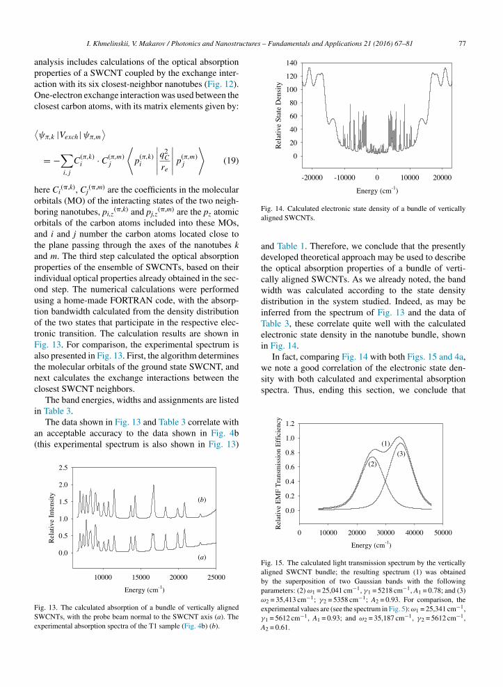
uctures – Fundamentals and Applications 21 (2016) 67–81 77
apaOc
⟨
hoboatapioutotFatnc
i
a(
FSe
Energy (cm-1)
-20000 -1 0000 0 1000 0 2000 0
Rel
ativ
e S
tate
Den
sity
0
20
40
60
80
100
120
140
In fact, comparing Fig. 14 with both Figs. 15 and 4a,we note a good correlation of the electronic state den-sity with both calculated and experimental absorptionspectra. Thus, ending this section, we conclude that
I. Khmelinskii, V. Makarov / Photonics and Nanostr
nalysis includes calculations of the optical absorptionroperties of a SWCNT coupled by the exchange inter-ction with its six closest-neighbor nanotubes (Fig. 12).ne-electron exchange interaction was used between the
losest carbon atoms, with its matrix elements given by:
ψπ,k |Vexch|ψπ,m⟩
= −∑i,j
C(π,k)i · C
(π,m)j
⟨p
(π,k)i
∣∣∣∣∣q2C
re
∣∣∣∣∣p(π,m)j
⟩(19)
ere Ci(�,k), Cj
(�,m) are the coefficients in the molecularrbitals (MO) of the interacting states of the two neigh-oring nanotubes, pi,z
(�,k) and pj,z(�,m) are the pz atomic
rbitals of the carbon atoms included into these MOs,nd i and j number the carbon atoms located close tohe plane passing through the axes of the nanotubes knd m. The third step calculated the optical absorptionroperties of the ensemble of SWCNTs, based on theirndividual optical properties already obtained in the sec-nd step. The numerical calculations were performedsing a home-made FORTRAN code, with the absorp-ion bandwidth calculated from the density distributionf the two states that participate in the respective elec-ronic transition. The calculation results are shown inig. 13. For comparison, the experimental spectrum islso presented in Fig. 13. First, the algorithm determineshe molecular orbitals of the ground state SWCNT, andext calculates the exchange interactions between thelosest SWCNT neighbors.
The band energies, widths and assignments are listedn Table 3.
The data shown in Fig. 13 and Table 3 correlate withn acceptable accuracy to the data shown in Fig. 4bthis experimental spectrum is also shown in Fig. 13)
(b)
Energy (cm-1)
10000 15000 20000 25000
Rel
ativ
e In
tens
ity
0.0
0.5
1.0
1.5
2.0
2.5
(a)
ig. 13. The calculated absorption of a bundle of vertically alignedWCNTs, with the probe beam normal to the SWCNT axis (a). Thexperimental absorption spectra of the T1 sample (Fig. 4b) (b).
Fig. 14. Calculated electronic state density of a bundle of verticallyaligned SWCNTs.
and Table 1. Therefore, we conclude that the presentlydeveloped theoretical approach may be used to describethe optical absorption properties of a bundle of verti-cally aligned SWCNTs. As we already noted, the bandwidth was calculated according to the state densitydistribution in the system studied. Indeed, as may beinferred from the spectrum of Fig. 13 and the data ofTable 3, these correlate quite well with the calculatedelectronic state density in the nanotube bundle, shownin Fig. 14.
(1)
Energy (cm-1)
0 1000 0 2000 0 3000 0 4000 0 5000 0
Rel
ativ
e E
MF
Tra
nsm
issi
on E
ffic
ienc
y
0.0
0.2
0.4
0.6
0.8
1.0
1.2
(2)
(3)
Fig. 15. The calculated light transmission spectrum by the verticallyaligned SWCNT bundle; the resulting spectrum (1) was obtainedby the superposition of two Gaussian bands with the followingparameters: (2) ω1 = 25,041 cm−1, γ1 = 5218 cm−1, A1 = 0.78; and (3)ω2 = 35,413 cm−1; γ2 = 5358 cm−1; A2 = 0.93. For comparison, theexperimental values are (see the spectrum in Fig. 5): ω1 = 25,341 cm−1,γ1 = 5612 cm−1, A1 = 0.93; and ω2 = 35,187 cm−1, γ2 = 5612 cm−1,A2 = 0.61.

78 I. Khmelinskii, V. Makarov / Photonics and Nanostructures – Fundamentals and Applications 21 (2016) 67–81
Table 3The band maxima, widths, and assignments for the calculated absorption spectrum of Fig. 14, and the SWCNT diameter used to obtain the respectiveband.
Number Band maximum,cm−1
Bandwidth, cm−1 Band assignment,(m,n)
Average nanotubediameter (nm)
Relative bandintensity
1 41,761 1611 (7,2) 3.1 0.08862 36,902 1721 (7,1) 3.3 0.05413 35,765 1625 (7,3) 3.7 0.04975 34,939 1603 (7,5) 2.7 0.05156 34,256 1731 (7,4) 3.1 0.06377 33,667 1613 (7,1) 3.5 0.06068 33,689 1651 (7,2) 4.2 0.05919 33,263 1636 (7,7) 2.5 0.0583
10 33,027 1710 (7,1) 2.8 0.058711 32,464 1627 (7,5) 3.8 0.054712 27,973 1612 (7,3) 4.6 0.033013 25,977 1612 (7,4) 3.1 0.023714 25,973 1612 (7,1) 3.3 0.021215 22,881 119 (5,5) 3.9 0.019916 20,785 129 (5,3) 2.8 0.019117 19,877 121 (4,1) 2.6 0.019218 18,279 122 (8,3) 2.7 0.021719 16,701 128 (6,5) 4.6 0.018020 16,721 127 (5,1) 2.8 0.020521 16,517 111 (9,5) 3.0 0.015922 14,243 173 (6,5) 2.7 0.013123 13,671 142 (10,5) 2.7 0.012624 11,479 121 (4,3) 3.6 0.023025 10,711 111 (8,1) 2.8 0.023126 10,103 143 (8,4) 2.9 0.021227 9407 129 (5,2) 3.0 0.018028 9057 129 (4,3) 2.7 0.036229 8389 153 (3,1) 2.8 0.021530 8209 128 (6,1) 2.6 0.020531 7779 127 (6,3) 4.7 0.0181
(7,1)
(7,3)
SWCNT bundle, and used to calculate the transmission
32 7363 111
33 6947 157
the presently developed approach may be used in theanalysis of the optical absorption properties of thevertically-aligned SWCNT bundles, with the exchangeinteractions between the closest-neighbor nanotubestaken into account.
Note that the mathematical procedure used for theband assignment, with the results presented in Table 3,may produce non-unique results. That is, the same spec-tral band could be assigned to more than one set of them and n values. However, we made test calculations,demonstrating that the results are indeed unique withinthe presently used diameter distribution of the nanotubes.A detailed numerical study was performed for the band#30 (8209 cm−1, m = 6, n = 1, and d = 2.6 nm). Varying m
and m in a broad range, we managed to obtain a band at8213 cm−1 for m = 73, n = 36, and d = 7.9 nm. The nano-tube diameter distribution was cut off at 10 nm in thesecalculations. However, the intensity of this band should3.0 0.01414.2 0.0197
be close to zero, due to negligible concentration of suchthick tubes in the sample. Thus, we conclude that theassignments of Table 3 are unique for the presently useddiameter distribution of the SWCNTs.
4.2. Analysis of the absorption spectrum of Fig. 6
The absorption spectrum shown in Fig. 6 correspondsto an efficient light transmission by the vertically alignedSWCNTs in the 20,000–40,000 cm−1 spectral range,with the light transmitted in the direction parallel tothe nanotube axis. To interpret these results, the earlierdeveloped theory [53] was modified, taking into accountthe electronic state structure of the vertically aligned
spectrum of the SWCNT bundle. The presently reportedtheoretical approaches were used in the numerical cal-culations. The earlier developed FORTRAN code [57]

uctures
wc
btdiasu
mdii
4
mwa3ed
ϑ
wcTweciT
5
vstbrhtstt
ma
I. Khmelinskii, V. Makarov / Photonics and Nanostr
as adapted to the present calculations, producing thealculated transmission spectrum shown in Fig. 15.
The calculated transmission spectrum was obtainedy the superposition of two Gaussian bands (Fig. 15)hat are in acceptable agreement with Gaussian bandsescribing the experimental absorption spectrum shownn Fig. 6. Thus, the presently developed theoreticalpproach is acceptable for the analysis of the transmis-ion spectra of bundles of vertically aligned SWCNTs,sing the light parallel to the nanotube axis.
To explain the presence of the two bands in the trans-ission spectrum, we should refer to the density of states
istribution of Fig. 13, with the two strong peaks locatedn the 10,000–20,000 cm−1 energy range, both contribut-ng to the emission propagating along the nanotube axis.
.2.1. The superemission divergenceThe SE beam divergence was measured using the
ethod developed earlier [23]. All of the measurementsere carried out for the T1 sample for the emission
t 5257 cm−1. The measured beam divergence was.9 × 10−3 and 5.2 × 10⁻⁴ rad, along the 0.02 and 0.2 cmdges of the sample, respectively. The limiting beamivergence was estimated using
= λ
πd(20)
here � is the SE wavelength and d is the geometri-al size of the SE beam at the output face of the sample.he calculated values are 7.6 × 10⁻⁴ and 7.6 × 10⁻⁵ rad,ith the experimental values exceeding the theoretic
stimates by the factor of 3.8 and 6.8, respectively, asommonly occurs for the superemission. Thus, the max-mum beam divergence was ca. 3.9 × 10⁻³ rad for the1 sample.
. Discussion
We report that the vertically aligned SWCNTs haveery interesting optical properties. We recorded theuperemission of the nanotube bundle upon laser excita-ion. The superemission spectrum has narrow emissionands; we presume that the emission bandwidth may beeduced still further by producing nanotubes with moreomogeneous properties. We found that the bundle ofhe VA SWCNTs, the T1 sample, has high superemis-ion energy and power density in the direction parallelo the nanotube axis, with the emission exiting through
he 0.02 cm × 0.2 cm faces.The superemission properties of the VA SWCNTsay be compared with those obtained for the VA single-
nd multi-wall carbon nanotubes [54–56]. Nojeh et al.
– Fundamentals and Applications 21 (2016) 67–81 79
[54–56] found that such nanotubes may be used as lightconcentrators, i.e. directing the excitation light normalto the nanotube axis, high-density radiation exits at theends of the nanotube. These effects are similar to whatwe observed earlier in metal nanolayers [18].
The results presently obtained for the verticallyaligned SWCNTs are the first step to building ananolaser. Lin et al. [57] investigated nanoscale opti-cal devices for classical and quantum photonics. Theydiscussed random lasers, where lasing relies on randommultiple scattering. Presently we have a well-organizedsystem, analyzed using the theoretical methods based onthe SSH theory successfully applied by Prylutsky et al.[12] to the optical spectra of SWCNTs. We modifiedtheir approach, by including the exchange interactionbetween the closest-neighbor nanotubes. The methodsdeveloped describe the optical spectra of the verticallyaligned SWCNTs with an acceptable accuracy. Note thatcalculated state density diagram has a specific structure,quite different from that reported by Prylutsky et al.[12]. Most probably, these differences result from theexchange interactions between the VA SWCNTs, closelypacked in our samples.
As it was mentioned above, the emission spectra andthe excited state dynamics of the isolated SWCNTs wereextensively studied earlier [28–46]. Taking into accountthat the photoemission quantum yield for the transitionbetween the quantum states |i〉 and |j〉 is given by:
ϕij(λ) = (τem,ij)−1
(τem,ij)−1 + knr(E)(21)
where τem,ij−1 is the inverse radiative lifetime of the
transition of interest and knr(E) is the nonradiative rateconstant describing the irreversible radiationless transi-tions from the state |j〉. It has been found earlier [31–35]for isolated SWCNTs that the relationship
(τem,ij)−1 << knr(E) (22)
is satisfied for the high-energy excited states, while forthe low-energy excited states we have:
(τem,ij)−1 < knr(E) (23)
The low-energy excited states are populated due tothe relaxation of the high-energy excited states, typicallyinduced by the exciton–phonon interaction. Presentlywe reported the emission spectra of the VA bundles ofSWCNTs for the first time. The observed photoemission
apparently results from the cooperative effects operat-ing in the samples studied. These cooperative effectsmay be created by strong interactions between the SWC-NTs organized into the VA bundle of macroscopic size.
uctures
[
[
[
[
[
[
[
[
[
[
[
[
[
[
[
80 I. Khmelinskii, V. Makarov / Photonics and Nanostr
Therefore, we do not have the microscopic quantum sys-tem any more, expecting different properties. The excitedstate energy and dynamics in such macroscopic systemsmay be dramatically different as compared to those ofisolated SWCNTs. Therefore, presently we are unableto exactly determine the nature of the optical transitionsthat are responsible for the observed superemission.
We address the reader to our previous publication [24]for the detailed discussion of the methods presently usedto calculate the transmission spectra in the longitudinaldirection.
6. Conclusions
In the present study, we investigated the NIR supere-mission in bundles of vertically aligned SWCNTs. Wereport that superemission is generated in the direction ofthe nanotube axis, when the pumping radiation is nor-mal to it. At the 3 mJ/pulse of the pumping laser energy,we obtained the SE at 0.74 mJ/pulse in the direction ofthe detector, corresponding to the total of 1.48 mJ/pulse.The energy and the power density were, respectively,18.5 mJ cm−2/pulse and 1.2 × 10⁵ W cm−2/pulse. Theseresults show that vertically aligned SWCNT bundlesshould be a good active medium for laser and nanolasersystems. The presently developed theoretical modelswere successfully used to fit both absorption and emis-sion spectra of the nanotube bundles. The divergence ofthe superemission was quite low, thus we have effec-tively obtained a single-pass laser, with the nanotubebundle being an efficient radiation energy concentrator.
Acknowledgements
The authors are grateful for the PR NASA EPSCoRgrant (NASA Cooperative Agreement NNX13AB22A)to V.M.
References
[1] X. Wang, Q. Li, J. Xie, Z. Jin, J. Wang, Y. Li, K. Jiang, S. Fan,Fabrication of Ultralong and Electrically Uniform Single-WalledCarbon Nanotubes on Clean Substrates, Nano Lett. 9 (2009)3137–3141, http://dx.doi.org/10.1021/nl901260b.
[2] R. Martel, V. Derycke, C. Lavoie, J. Appenzeller, K. Chan, J. Ter-soff, P. Avouris, Ambipolar electrical transport in semiconductingsingle-wall carbon nanotubes, Phys. Rev. Lett. 87 (2001) 256805,http://dx.doi.org/10.1103/PhysRevLett.87.256805.
[3] M.S. Dresselhaus, Nanotechnology: new tricks with nanotubes,Nature 391 (1998) 19–23.
[4] C.T. White, J.W. Mintmire, Density of states reflects diameter innanotubes, Nature 394 (1998) 29–37.
[5] J.W.G. Wildoer, et al., Electronic structure of atomically resolvedcarbon nanotube, Nature 391 (1998) 59–67.
[
– Fundamentals and Applications 21 (2016) 67–81
[6] R. Saito, M. Fujita, G. Dresselhaus, M.S. Dresselhaus, Tight-binding model for carbon nanotubes from ab initio calculations,Phys. Rev. B Condens. Matter 46 (1992) 1804–1921.
[7] C.L. Kane, E.J. Mele, Ratio problem in single carbon nano-tube fluorescence spectroscopy, Phys. Rev. Lett. 90 (2003)207401–207407.
[8] S. Yokojima, G.H. Chen, Linear-scaling localized-density-matrixmethod for the ground and excited states of one-dimensionalmolecular systems, Chem. Phys. Lett. 300 (1999) 540–549.
[9] W.Z. Liang, S. Yokojima, D.H. Zhou, G.H. Chen, Localized-density-matrix method and its application to carbon nanotubes, J.Phys. Chem. A 104 (2000) 2445–2453.
10] W. Liang, G. Chen, Z. Li, Z.-K. Tang, Absorption spectra andchirality of single-walled 4 A carbon nanotubes, Appl. Phys. Lett.80 (2000) 3415–3427.
11] Y. Zhao, X.J. Wang, C.-C. Ma, G.H. Chen, Absorption spectralfeature of single wall carbon nanotubes, Chem. Phys. Lett. 387(2004) 149–154.
12] Yu.I. Prylutsky, O.V. Ogloblya, P. Sharfe, Computer modelling ofthe optical absorption spectrum of single-walled carbon nanotubebundles, ISSN 0503-1265, Ukr. J. Phys. 49 (2004) A17–A28.
13] M. Meyyappan, Carbon Nanotubes: Science and Applications,July 28, 2004 by CRC Press, Reference – 310 Pages – 188 B/WIllustrations ISBN 9780849321115 – CAT# 2111.
14] A.A. Tonkikh, V.I. Tsebro, E.A. Obraztsova, K. Suenaga, H.Kataura, A.G. Nasibulin, E.I. Kauppinen, E.D. Obraztsova,Metallization of single-wall carbon nanotube thin filmsinduced by gas phase iodination, Carbon 94 (2015) 768–774,http://dx.doi.org/10.1016/j.carbon.2015.07.062.
15] A. Roch, L. Stepien, T. Roch, I. Dani, C. Leyens, O. Jost, A.Leson, Optical absorption spectroscopy and properties of singlewalled carbon nanotubes at high temperature, Synth. Metals 197(2014) 182–187.
16] A.V. Naumov, S. Ghosh, D.A. Tsyboulski, S.M. Bachilo, R.B.Weisman, One-dimensional silver nanostructures on single-wallcarbon nanotubes, ACS Nano J. 5 (2011) 1639–1648.
17] W. Zhou, D. Nakamura, H. Liu, H. Kataura, S. Takeyama,Relative ordering between bright and dark excitons in single-walled carbon nanotubes, Sci. Rep. 4 (6999) (2014) 1–6,http://dx.doi.org/10.1038/srep06999.
18] I.V. Khmelinskii, V.I. Makarov, Superemission of Cr Nanolayers,Mater. Res. Bull. (2016) (in print March 29).
19] R. Saito, G. Dresselhaus, M.S. Dresselhaus, Physical Propertiesof Carbon Nanotubes, Imperial College Press, London, 1998.
20] M.S. Dresselhaus, G. Dresselhaus, Ph. Avouris (Eds.), CarbonNanotubes: Synthesis, Structure, Properties, and Applications,Springer-Verlag, New York, 2001.
21] A. Ugawa, A. Rinzler, D.B. Tanner, Far-infrared gaps insingle-wall carbon nanotubes, Phys. Rev. B 60 (1999)R11305–R11308.
22] M.E. Itkis, S. Niyogi, M.E. Meng, M.A. Harmon, H. Hu, R.C.Haddon, Spectroscopic study of the Fermi level electronic struc-ture of single-walled carbon nanotubes, Nano Lett. 2 (2002)155–159.
23] C.L. Kane, E.J. Mele, Size, shape, and low energy electronic struc-ture of carbon nanotubes, Phys. Rev. Lett. 78 (1997) 1932–1935.
24] Th. Pichler, M. Knupfer, M.S. Golden, J. Fink, A. Rinzler, R.E.Smalley, Localized and delocalized electronic states in single-
wall carbon nanotubes, Phys. Rev. Lett. 80 (1998) 4729–4732.25] Y. Murakami, E. Einarsson, T. Edamura, S. Maruyama, Polariza-tion dependence of the optical absorption of single-walled carbonnanotubes, Phys. Rev. Lett. 94 (2005), 087402/1–087402/4.1.

uctures
[
[
[
[
[
[
[
[
[
[
[
[
[
[
[
[
[
[
[
[
[
[
[
[
[
[
[
[
[
[
[
[57] J. Liu, P.D. Garcia, S. Ek, N. Gregersen, T. Suhr, M. Schu-bert, J. Mørk, S. Stobbe, P. Lodahl, Plasmon-induced hot carrier
I. Khmelinskii, V. Makarov / Photonics and Nanostr
26] J.B. Birks, Photophysics of Aromatic Molecules, Wiley, London,1970.
27] Y.-Z. Ma, J. Stenger, J. Zimmerman, S.M. Bachilo, R.E. Smal-ley, R.B. Weisman, G.R. Fleming, Ultrafast carrier dynamics insingle-walled carbon nanotubes probed by femtosecond spec-troscopy, J. Chem. Phys. 120 (2004) 3368–3372.
28] S. Reich, M. Dworzak, A. Hoffmann, C. Thomsen, M.S. Strano,Excited-state carrier lifetime in single-walled carbon nanotubes,Phys. Rev. B 71 (2005), 033402/1 - 033402/4. 25.
29] J.-P. Yang, M.M. Kappes, H. Hippler, A.-N. Unterreiner, Fem-tosecond transient absorption spectroscopy of single-walledcarbon nanotubes in aqueous surfactant suspensions: determina-tion of the lifetime of the lowest excited state, Phys. Chem. Chem.Phys. 7 (2005) 512–517.
30] G.N. Ostojic, S. Zaric, J. Kono, M.S. Strano, V.C. Moore, R.H.Hauge, R.E. Smalley, Interband recombination dynamics in res-onantly excited single-walled carbon nanotubes, Phys. Rev. Lett.92 (2004), 117402/1–117402/4.
31] F. Wang, G. Dukovic, L.E. Brus, T.F. Heinz, The optical reso-nances in carbon nanotubes arise from excitons, Science 5723(2005) 838–841.
32] A.M. Rao, E. Richter, S. Bandow, B. Chase, P.C. Eklund, K.A.Williams, S. Fang, K.R. Subbaswamy, M. Menon, A. Thess, R.E.Smalley, G. Dresselhaus, M.S. Dresselhaus, Diameter-selectiveRaman scattering from vibrational modes in carbon nanotubes,Science 275 (1997) 187–191.
33] M.S. Dresselhaus, G. Dresselhaus, A. Jorio, A.G. Souza Filho,R. Saito, Raman spectroscopy on isolated single wall carbonnanotubes, Carbon 40 (2002) 2043–2061.
34] C.L. Kane, E.J. Mele, Ratio problem in single carbon nano-tube fluorescence spectroscopy, Phys. Rev. Lett. 90 (2003)207401–207407.
35] M. O’Connell, S.M. Bachilo, C.B. Huffman, V. Moore, M.S.Strano, E. Haroz, K. Rialon, P.J. Boul, W.H. Noon, C. Kittrell, J.Ma, R.H. Hauge, R.B. Weisman, R.E. Smalley, Band-gap fluores-cence from individual single-walled carbon nanotubes, Science297 (2002) 593–596.
36] H. Htoon, M.J. O’Connell, S.K. Doorn, V.I. Klimov, Singlecarbon nanotubes probed by photoluminescence excitation spec-troscopy: the role of phonon-assisted transitions, Phys. Rev. Lett.94 (2005), 127403/1–127403/4.
37] M. Jones, C. Engtrakul, W.K. Metzger, R.J. Ellingson, A.J. Nozik,M.J. Heben, G. Rumbles, Analysis of photoluminescence fromsolubilized single-walled carbon nanotubes, Phys. Rev. B 71(2005), 115426/1–115426/9.
38] J. Lefebvre, P. Finnie, Y. Homma, Temperature-dependent pho-toluminescence from single-walled carbon nanotubes, Phys. Rev.B 70 (2004), 045419/1–045419/8.
39] R.B. Weisman, S.M. Bachilo, D. Tsyboulski, Fluorescencespectroscopy of single-walled carbon nanotubes in aqueous sus-pension, Appl. Phys. A 78 (2004) 1111–1116.
40] J. Lefebvre, J.M. Fraser, Y. Homma, P. Finnie, Photoluminescencefrom single-walled carbon nanotubes: a comparison between sus-pended and micelle-encapsulated nanotubes, Appl. Phys. A 78(2004) 1107–1110.
41] J. Lefebvre, J.M. Fraser, P. Finnie, Y. Homma, Photoluminescencefrom an individual single-walled carbon nanotube, Phys. Rev. B69 (2004), 075403/1–075403/5.
42] T. Ando, Excitons in carbon nanotubes, J. Phys. Soc. Jpn. 66(1997) 1066–1073.
– Fundamentals and Applications 21 (2016) 67–81 81
43] C.D. Spataru, S. Ismail-Beigi, L.X. Benedict, S.G. Louie,Excitonic effects and optical spectra of single-walled carbonnanotubes, Phys. Rev. Lett. 92 (2004), 077402/1–077402/4.
44] V. Perebeinos, J. Tersoff, P. Avouris, Scaling of excitons in carbonnanotubes, Phys. Rev. Lett. 92 (2004), 257402/1–257402/4.
45] Y.-Z. Ma, L. Valkunas, S.L. Dexheimer, S.M. Bachilo, G.R.Fleming, Femtosecond spectroscopy of optical excitations insingle-walled carbon nanotubes: evidence for exciton–excitonannihilation, Phys. Rev. Lett. 94 (2005), 157402/1–157402/4.
46] V. Perebeinos, J. Tersoff, P. Avouris, Radiative lifetime of excitonsin carbon nanotubes, Los Alamos National Laboratory PreprintArchive, Condens. Matter (2005), 0506775/1–0506775/4.
47] C. Manzoni, A. Gambetta, E. Menna, M. Meneghetti, G. Lan-zani, G. Cerullo, Intersubband exciton relaxation dynamics insingle-walled carbon nanotubes, Phys. Rev. Lett. 94 (2005),207401/1–207401/4.
48] H. Liu, T. Tanaka, H. Kataura, Optical isomer separa-tion of single-chirality carbon nanotubes using gel col-umn chromatography, Nano Lett. 14 (2014) 6237–6243,http://dx.doi.org/10.1021/nl5025613.
49] H. Kuzmany, W. Plank, M. Hulman, Determination of SWCNTdiameters from the Raman response of the radial breathing mode,Eur. Phys. J. B 22 (2001) P307–P320.
50] Y.-S. Lim, A.R.T. Nugraha, S.-J. Cho, M.-Y. Noh, E.-J. Yoon,H. Liu, J.-H. Kim, H. Telg, E.H. Haroz, G.D. Sanders, S.-H. Baik, H. Kataura, S.K. Doorn, C.J. Stanton, R. Saito,J. Kono, T. Joo, Ultrafast generation of fundamental andmultiple-order phonon excitations in highly-enriched (6,5) single-wall carbon nanotubes, Nano Lett. 14 (2014) 1426–1432,http://dx.doi.org/10.1021/nl404536b.
51] M. Sauer, H. Shiozawa, P. Ayala, H. Ruiz-Soria, X. Liu,K. Yanagi, H. Kataura, S. Krause, T. Pichler, Environmentalstability of ferrocene filled in purely metallic single-walled car-bon nanotubes, Phys. Status Solidi B 250 (2013) 2599–2604,http://dx.doi.org/10.1002/pssb.201300124.
52] T. Hertel, R. Fasel, G. Moos, Exciton transfer and propagation incarbon nanotubes studied by near-field optical microscopy, Appl.Phys. A. 75 (2002) P449–P465.
53] V. Makarov, L. Zueva, T. Golubeva, E. Korneeva, I. Khmelinskii,M. Inyushin, Quantum mechanism of light transmission by theintermediate filaments in some specialized optically transparentcells, Neurophotonics J. (2016) (in press).
54] M. Chang, P. Yaghoobi, W. Khalid, A. Nojeh, The synthesisof vertically aligned multi-walled carbon nanotube forests bythermal chemical vapor deposition, in: A. Mishra (Ed.), CarbonNanotubes: Synthesis, Properties and Applications, Nova SciencePublishers Inc., 2012.
55] A.H. Khoshaman, A.T. Koch, M. Chang, H.D.E. Fan, M.V.Moghaddam, A. Nojeh, Nanostructured thermionics for con-version of light to electricity: simultaneous extraction ofdevice parameters, IEEE Trans. Nanotechnol. 14 (2015)624–632.
56] M. Vahdani Moghaddam, P. Yaghoobi, G.A. Sawatzky, A. Nojeh,Photon-impenetrable, electron-permeable: the carbon nanotubeforest as a medium for multi-photon thermal-photoemission, ACSNano 9 (2015) 4064–4069.
science and technology, Nat. Nanotechnol. 9 (2014) 285–289,http://dx.doi.org/10.1038/nnano.2014.34.