surface-plasmon waveguides for biosensor applications
TRANSCRIPT

Surface-plasmon waveguides (Fourth Lecture) Techno Forum on Micro-optics and Nano-optics Technologies
p gfor biosensor applications
송 석 호 한양대학교 물리학과 http://optics anyang ac kr/~shsong송 석 호, 한양대학교 물리학과, http://optics.anyang.ac.kr/~shsong
metal stripmetal slab
Y-branchS-band
metal slab
Metal SPP waveguide
300
350
Output signal
50
100
150
200
250
Inte
nsity
(uW
)
1. How do we define the dispersion relations of SPPs excited on thin metal films and stripes?
1.330 1.331 1.332 1.333 1.334 1.335 1.3360
Refractive index of waterReference arm Sensing arm
p p2. What are the long-range SPPs and short-range SPPs?2. How can we implement LRSPP waveguide devices?4. What are the merits of the LRSPP waveguide-type sensors?
Key notes
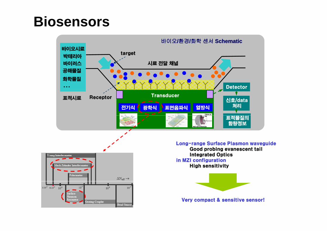
Biosensors
시료 전달 채널
바이오시료
박테리아
바이러스
target
바이오바이오//환경환경//화학화학 센서센서 SchematicSchematic
시료 전달 채널바이러스
공해물질
화학물질
… Detector
Transducer표적시료 신호/data
처리
Receptor
전기식 광학식 표면음파식 열방식
표적물질의함량정보
L S f Pl idLong-range Surface Plasmon waveguideGood probing evanescent tailIntegrated Optics
in MZI configurationHigh sensitivityg y
Very compact & sensitive sensor!

휴대폰용 Biosensors당뇨폰
음주측정폰
입냄새폰
Conventional prism-type SPR sensorsConventional prism type SPR sensors

Surface Plasmon Resonance Sensors시료 불감지 시
Convergentlight beam
Photodiode array
시료 감지시
Prism coupler
SPR-active metal
SPSample
Biomolecularrecognition
elements
시료 농도 변화 ~ sensing layer 유전율 변화 ~ SPR 공명각 변화량- Angle interrogation- Wavelength interrogation
Best SPR sensor:
BiaCoreAngle interrogationΔnmin~3x10⁻⁷
Large sizeLarge sizeExpensive (장비:2억, chip 10만원)
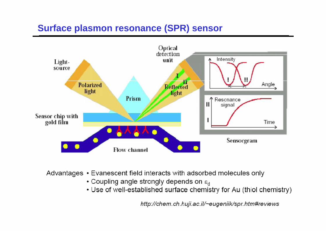
Surface plasmon resonance (SPR) sensor
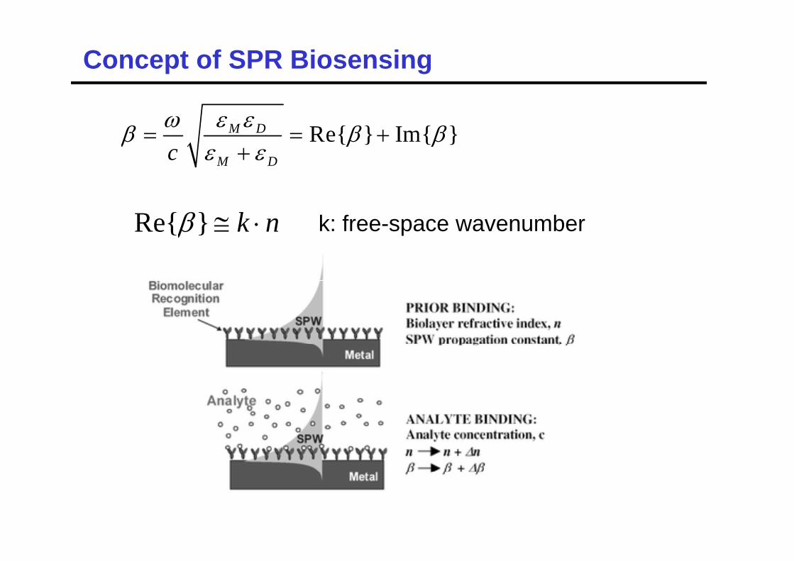
Concept of SPR Biosensing
Re{ } Im{ }M D
cω ε εβ β β
ε ε= = +
+M Dc ε ε+
R { } kβ k f bRe{ } k nβ ≅ ⋅ k: free-space wavenumber
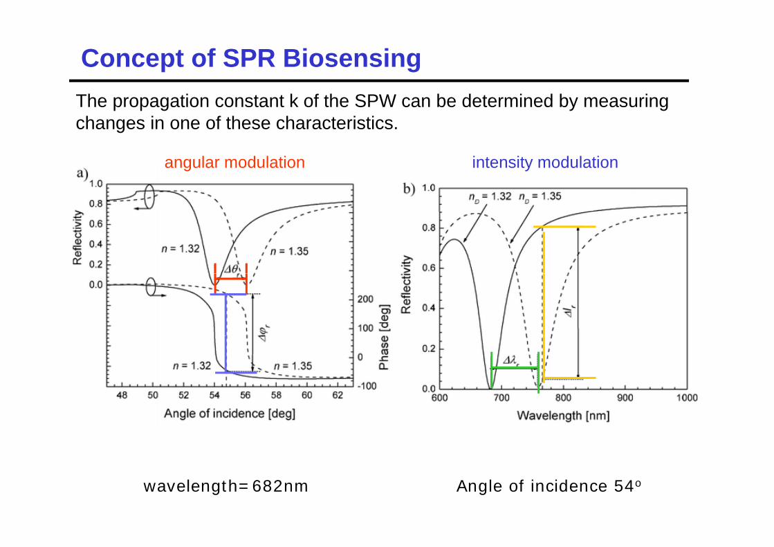
Concept of SPR BiosensingThe propagation constant k of the SPW can be determined by measuring changes in one of these characteristics.
angular modulation intensity modulation
wavelength=682nm Angle of incidence 54o

SPR imaging
• Spatially-filtered, expanded, l i d H N lp-polarized HeNe laser
beam illuminates the gold sample through a prism couplercoupler.
• Reflected light from the gold surface, containing the SPR image, is monitored with a CCD camera.
• The angle of incidence can be changed by rotating the g y gentire sample assembly.
A.J. Thiel et. al., Anal. Chem. 69 (1997), pp. 4948–4956.
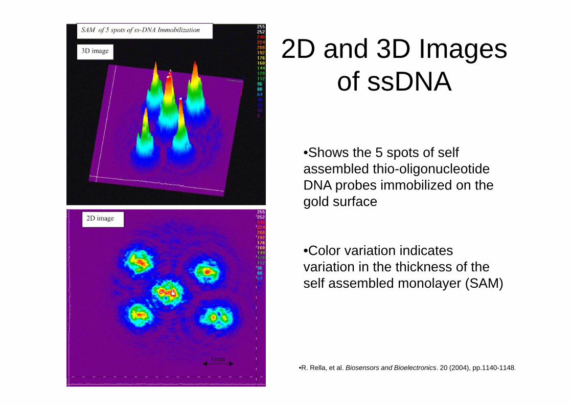
2D and 3D Images of ssDNA
•Shows the 5 spots of selfShows the 5 spots of self assembled thio-oligonucleotide DNA probes immobilized on the gold surfacegold surface
Color variation indicates•Color variation indicates variation in the thickness of the self assembled monolayer (SAM)
•R. Rella, et al. Biosensors and Bioelectronics. 20 (2004), pp.1140-1148.
Surface plasmon-polaritons excited on thin metal filmsSurface plasmon polaritons excited on thin metal filmswith IMI (insulator-metal-insulator) structures
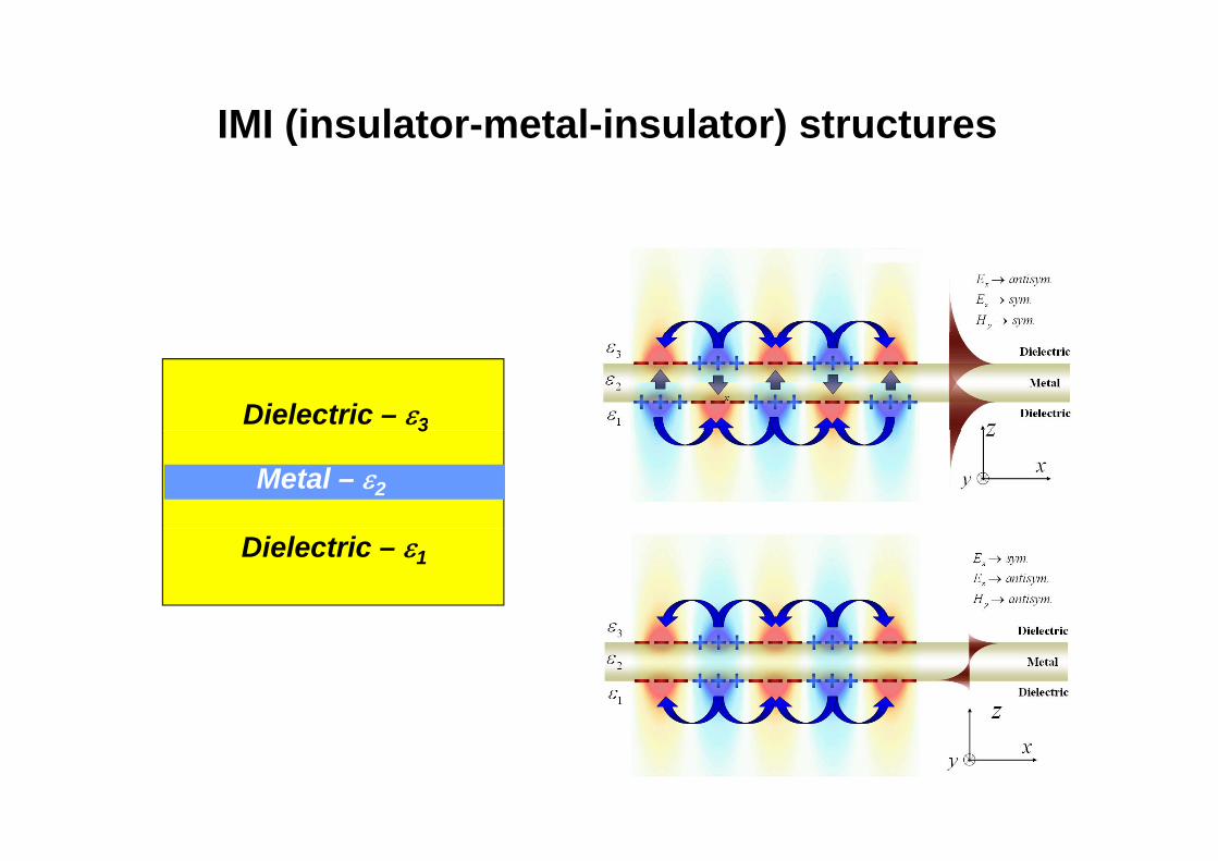
IMI (insulator-metal-insulator) structuresIMI (insulator metal insulator) structures
Dielectric – ε33
Metal – ε2
Dielectric – ε1
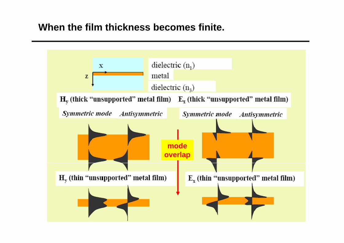
When the film thickness becomes finite.
modeoverlap

Long-range SPP and short-range SPPg g g
Long-Range SPP:Long-Range SPP: weak surface confinement, low loss
yeq
uenc
yfr
e
Short-Range SPP:strong surface confinement, high loss
in-plane wavevector
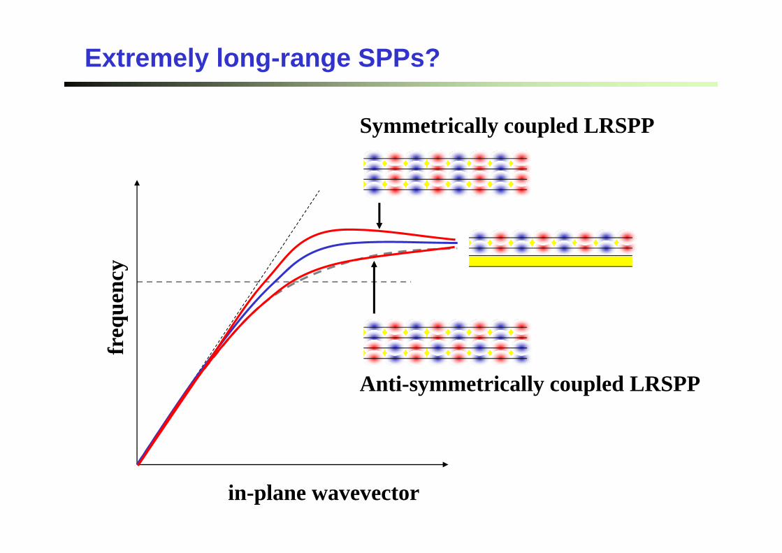
Extremely long-range SPPs?
Symmetrically coupled LRSPPcy
requ
enc
fr
Anti-symmetrically coupled LRSPP
in-plane wavevector

Dependence of dispersion on film thickness
0 75
1
0 75
1
0 75
1
0 75
1
200 400 600 800
-0.25
0.25
0.5
0.75
200 400 600 800
-0.25
0.25
0.5
0.75
250 500 750 1000 1250 1500
-0.25
0.25
0.5
0.75
250 500 750 1000 1250 1500
-0.25
0.25
0.5
0.75
practically forbidden-1
-0.75
-0.5
-1
-0.75
-0.5
60h nm=-1
-0.75
-0.5
-1
-0.75
-0.5
10h nm=
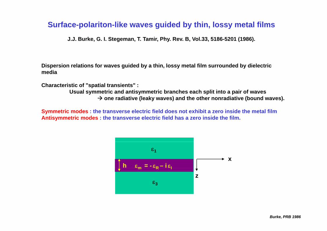
Surface-polariton-like waves guided by thin, lossy metal films
G S ( )J.J. Burke, G. I. Stegeman, T. Tamir, Phy. Rev. B, Vol.33, 5186-5201 (1986).
Dispersion relations for waves guided by a thin, lossy metal film surrounded by dielectric media
Characteristic of "spatial transients" : Usual symmetric and antisymmetric branches each split into a pair of waves
one radiative (leaky waves) and the other nonradiative (bound waves).
Symmetric modes : the transverse electric field does not exhibit a zero inside the metal filmAntisymmetric modes : the transverse electric field has a zero inside the film.
εm = - εR – i εIhx
ε1
m R I
zε3
Burke, PRB 1986
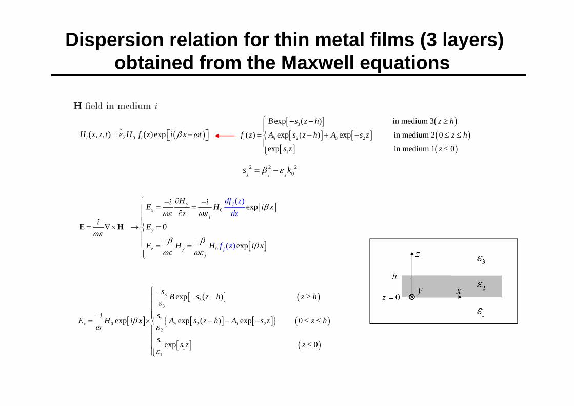
Dispersion relation for thin metal films (3 layers)obtained from the Maxwell equationsobtained from the Maxwell equations
( )0( , , ) ( )expyi iH x z t e H f z i x tβ ω= −⎡ ⎤⎣ ⎦
[ ] ( )[ ] [ ] ( )
[ ] ( )
3
2 0 2
1
exp ( ) in medium 3
( ) exp ( ) exp in medium 2 0
exp in medium 1 0i h
B s z h z h
f z A s z h A s z z h
s z z
⎧ − − ≥⎪
= − + − ≤ ≤⎨⎪ ≤⎩
2 2 20j j js kβ ε= −
[ ]( )jHi i df z∂⎧ − − [ ]
[ ]
0
0
exp
0
( )
( ) exp
yx
j
y
z y
j
j
Hi iE H i xz
i E
E H
d
H i x
f zdz
f z
βωε ωε
ωεβ β β
∂⎧= =⎪ ∂⎪
⎪= ∇× → =⎨⎪ − −⎪ = =⎪
E H
[ ]0 ( ) pz yj
jf βωε ωε⎪⎩
[ ] ( )3 ( )s B h h⎧−
≥⎪
[ ]
[ ] ( )
[ ] [ ]{ } ( )
[ ] ( )
33
3
20 2 0 2
2
1
exp ( )
exp exp ( ) exp 0x h
B s z h z h
siE H i x A s z h A s z z h
s
ε
βω ε
− − ≥⎪⎪⎪− ⎪= × − − − ≤ ≤⎨⎪⎪⎪ [ ] ( )1
11
exp 0s s z zε
≤⎪⎪⎩
From the boundary conditions,
( )( )
1 2 2 0
2 3 2 0
0 : exp[ ] 1
: exp[ ]x x h
x x h
z H H s h A A
z h H H A s h A B
= = ⇒ − + =⎧⎪⎨
= = ⇒ + − =⎪⎩
2 11 2 2 0
1 2
2 32 3 2 0
0 : exp[ ]
: exp[ ]
x x h
x x h
sz E E s h A As
sz h E E A s h A B
εεε
⎧ = = ⇒ − − =⎪⎪⎨⎪ = = ⇒ − − = −⎪⎩ 3 2sε⎪⎩
⎧⎛ ⎞
From the equations at z = 0, Ah, Ao, and B can be determined by,
[ ] [ ] [ ] ( )
[ ] [ ] ( )
2 12 2 3
1 2
2 12 2
1 2
cosh sinh exp ( ) 3:
( ) cosh sinh 2 : 0j
ss h s h s z h j z hs
sf z s z s z j z hs
εεεε
⎧⎛ ⎞+ − − = ≥⎪⎜ ⎟
⎝ ⎠⎪⎪⎪= + = ≤ ≤⎨⎪
[ ] ( )1exp 1: 0s z j z⎪⎪ = ≤⎪⎪⎩
Therefore, anther equations at z = h gives the dispersion relation,
( ) [ ] ( )2 21 3 2 2 1 3 2 2 2 3 1 1 3tanh 0s s s s h s s sε ε ε ε ε ε+ + + =( ) [ ] ( )1 3 2 2 1 3 2 2 2 3 1 1 3
2 2 20j j js kβ ε= −
ε1
εm
Hy
ε1
εm
Hy
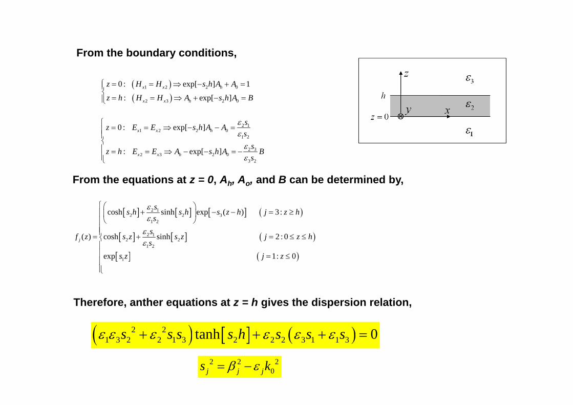
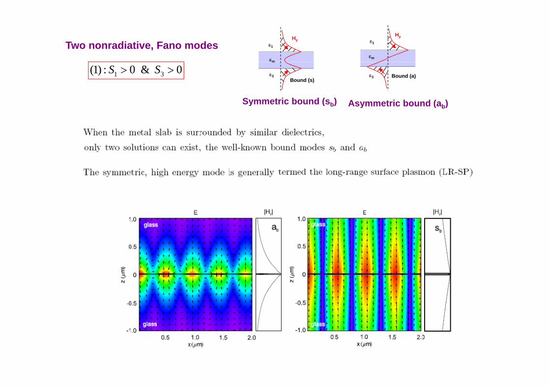
Two nonradiative, Fano modes
ε3 Bound (a)
m
ε3Bound (s)
1 3(1) : 0 & 0S S> >
Symmetric bound (sb) Asymmetric bound (ab)y ( b) Asymmetric bound (ab)

Surface plasmon dispersion for thin filmsDrude model
ε1(ω)=1-(ωp/ω) 2Two modes appear
L-(asymmetric)
Thinner film:
L+(symmetric)
Thinner film:Shorter SP wavelength
Propagation
L
Example:λHeNe = 633 nm
λSP = 60 nm
Propagationlengths: cm !!!(infrared)
L-λSP = 60 nm

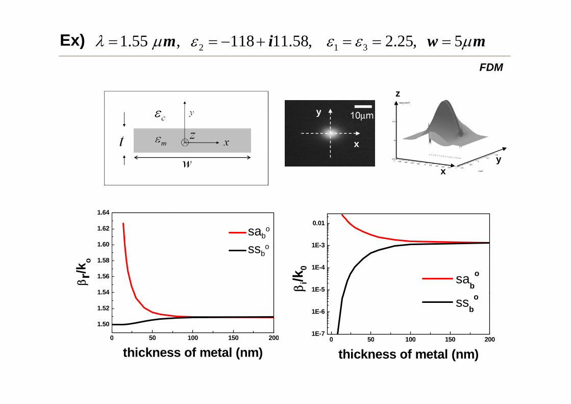
2 1 31.55 , 118 11.58 2.25 , m iλ μ ε ε ε= = − + = =Ex)
( ) [ ] ( )2 21 3 2 2 1 3 2 2 2 3 1 1 3tanh 0s s s s h s s sε ε ε ε ε ε+ + + =
H
sb ab
2 2 20j j js kβ ε= − ε1
εm
ε3
Hy
Bound (a)
ε1
εm
ε3
Hy
Bound (s)
2.0
1
a
( )Bound (s)
1.8
1.9ab
sb
k 0 1E 3
0.01
0.1ab
sb
k 01.6
1.7 β r/k
1E-5
1E-4
1E-3
β i/k
0 50 100 150 200
1.5
( )0 50 100 150 200
1E-7
1E-6
thickness (h : nm) thickness (h : nm) thickness (h : nm)

Metal stripe waveguides usingMetal stripe waveguides usinglong-range surface plasmon polaritons(LRSPPs)
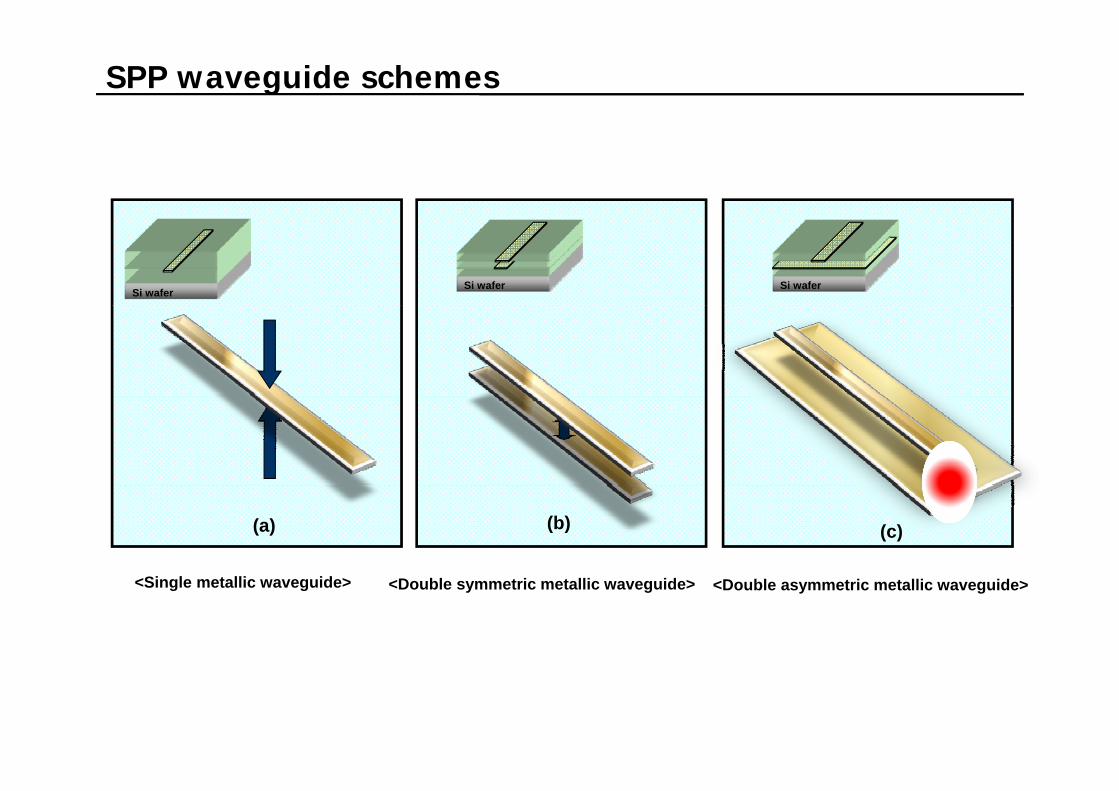
SPP waveguide schemes
Si waferSi waferSi wafer
(a) (c)(b)
<Single metallic waveguide> <Double symmetric metallic waveguide> <Double asymmetric metallic waveguide>
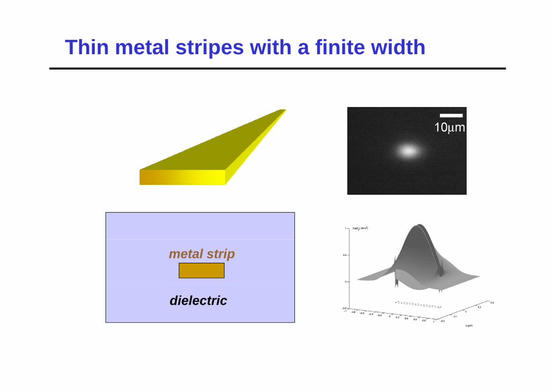
Thin metal stripes with a finite width
metal strip
dielectric
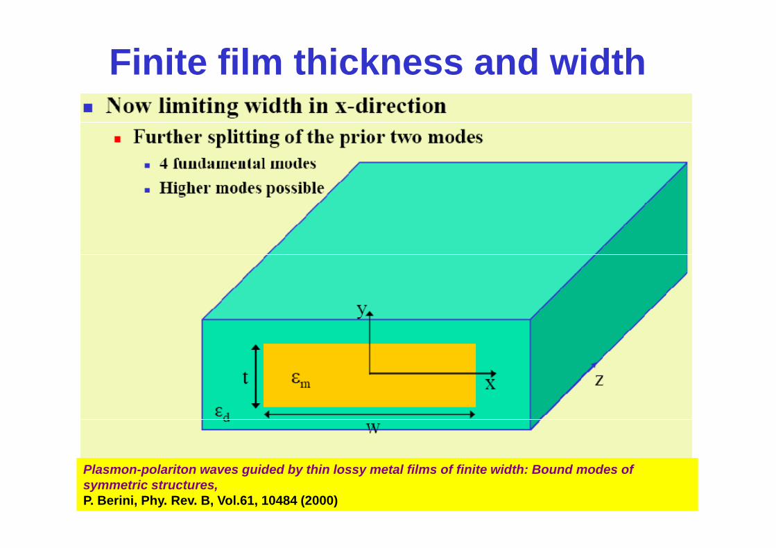
Finite film thickness and width
Plasmon-polariton waves guided by thin lossy metal films of finite width: Bound modes of symmetric structures,P. Berini, Phy. Rev. B, Vol.61, 10484 (2000)
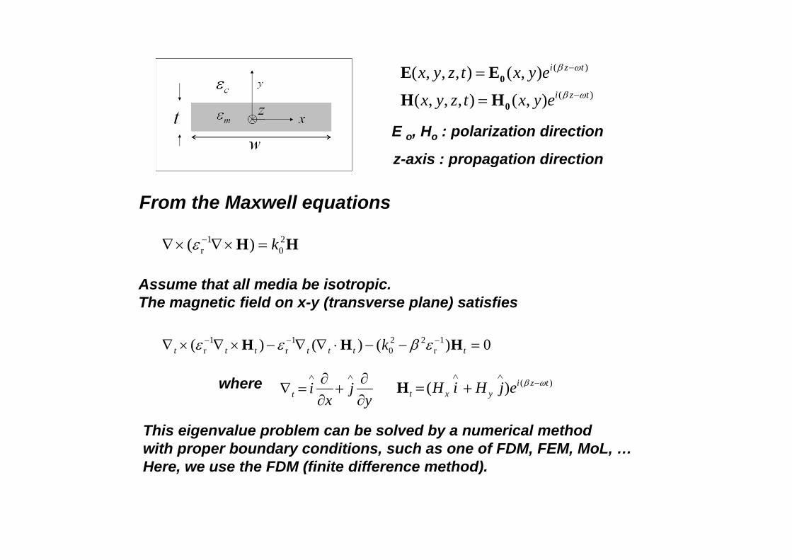
( )( , , , ) ( , ) i z tx y z t x y e β ω−= 0E E( )( , , , ) ( , ) i z tx y z t x y e β ω−= 0H H
E o, Ho : polarization direction
z-axis : propagation direction
From the Maxwell equations
1 2r 0( ) kε −∇× ∇× =H H
A th t ll di b i t i
1 1 2 2 1( ) ( ) ( ) 0kε ε β ε− − −∇ × ∇ × ∇ ∇H H H
Assume that all media be isotropic.The magnetic field on x-y (transverse plane) satisfies
r r 0 r( ) ( ) ( ) 0t t t t t t tkε ε β ε∇ × ∇ × − ∇ ∇ ⋅ − − =H H H
t i jx y
∧ ∧∂ ∂∇ = +
∂ ∂( )( ) i z t
t x yH i H j e β ω∧ ∧
−= +Hwherey
This eigenvalue problem can be solved by a numerical method with proper boundary conditions, such as one of FDM, FEM, MoL, …Here, we use the FDM (finite difference method).Here, we use the FDM (finite difference method).
FDM
2 1 31.55 , 118 11.58, 2.25, 5 m i w mλ μ ε ε ε μ= = − + = = =Ex)FDM
y
z
y
x
xy
1.60
1.62
1.64
sabo
ss o 1E-3
0.01
1.54
1.56
1.58
β r/k
o
ssbo
1E-5
1E-4
β i/k
0
sabo
0 50 100 150 200
1.50
1.52
1.54
0 50 100 150 2001E-7
1E-6 ssb
o
0 50 100 150 200
thickness of metal (nm)0 50 100 150 200
thickness of metal (nm)
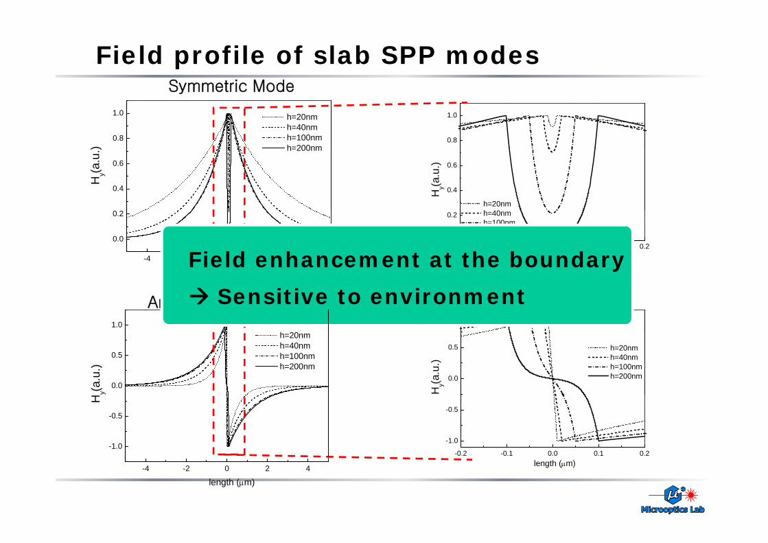
Field profile of slab SPP modesSymmetric Mode
0.8
1.0
)
h=20nm h=40nm h=100nmh=200nm
0.8
1.0
Symmetric Mode
0.4
0.6
Hy(a
.u.) h=200nm
0.4
0.6
Hy(a
.u.)
h=20nm
-4 -2 0 2 4
0.0
0.2
length ( m)
-0.2 -0.1 0.0 0.1 0.20.0
0.2
length (μm)
h=40nm h=100nm h=200nm
Field enhancement at the boundary
1.0h 20
length (μm)
1.0
Anti-Symmetric Mode
y
Sensitive to environment
0.0
0.5
h=20nm h=40nm h=100nm h=200nm
y(a.u
.)
0.0
0.5
h=20nm h=40nm h=100nm h=200nm
Hy(a
.u.)
-1.0
-0.5
H
-0.2 -0.1 0.0 0.1 0.2
-1.0
-0.5
-4 -2 0 2 4
length (μm)
length (μm)

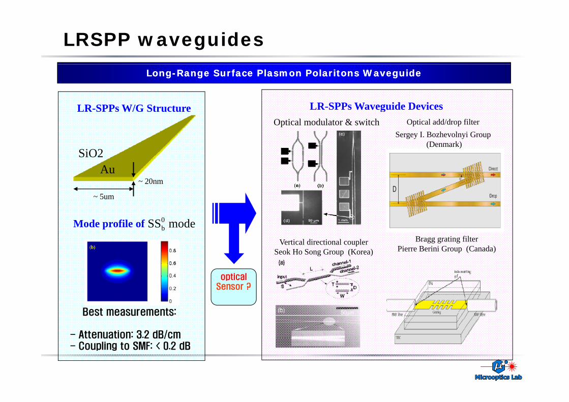
LRSPP waveguidesLongLong--Range Surface Plasmon Polaritons WaveguideRange Surface Plasmon Polaritons Waveguide
LR-SPPs W/G Structure LR-SPPs Waveguide Devices
SiO2
LR SPPs W/G Structure S s W vegu de ev cesOptical modulator & switch
Sergey I. Bozhevolnyi Group(Denmark)
Optical add/drop filter
SiO2Au
~ 20nm
~ 5um
mode SS0bMode profile of
Bragg grating filterPi B i i G (C d )
Vertical directional couplerPierre Berini Group (Canada)Seok Ho Song Group (Korea)
optical Sensor ?
Best measurements:
- Attenuation: 3.2 dB/cmAttenuation 3.2 dB/cm- Coupling to SMF: < 0.2 dB
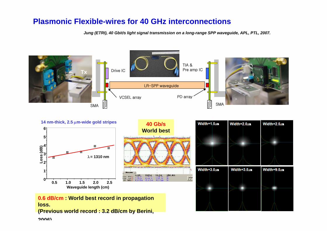
Jung (ETRI), 40 Gbit/s light signal transmission on a long-range SPP waveguide, APL, PTL, 2007.
Plasmonic Flexible-wires for 40 GHz interconnections
LR-SPP waveguide
Drive IC
TIA & Pre amp ICTx
VCSEL array
SMA SMA
PD array
Rx
14 nm-thick, 2.5 μm-wide gold stripes
5
640 Gb/s
World best
2
3
4
Loss
(dB
)
λ= 1310 nm
0.5 1.0 1.5 2.0 2.50
1
Waveguide length (cm)
0.6 dB/cm : World best record in propagation loss. (Previous world record : 3.2 dB/cm by Berini, 2006)

Double-electrode metal waveguides : Lines, S-band, Y-branchJoo, Long-range surface -plasmon--polaritons on asymmetric double-electrode structures, APL, 2008.
εd3 ε2D
wSPP mode
metal strip
εd3
D
metal slab
core
cladding
εd1
metal strip
Y-branchS-band
pmetal slab
LRSPP waveguide sensorsLRSPP waveguide sensors
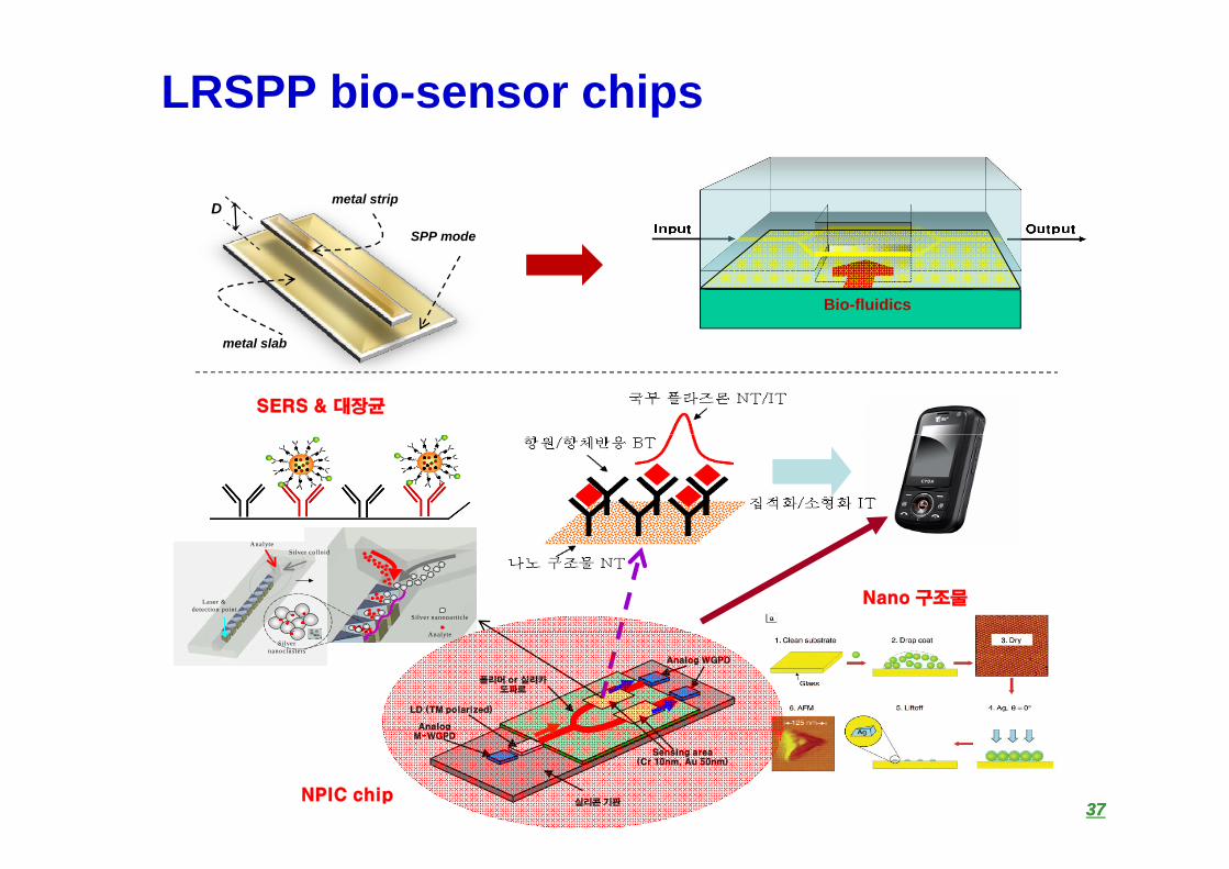
LRSPP bio-sensor chips
D
SPP mode
metal strip
Bio-fluidics
SPP mode
metal slab
SERS & 대장균
Silver nanoparticle
Silver colloid Analyte
Laser & detection point
Nano 구조물
Analog
Analog WGPD
LD (TM polarized)
폴리머 or 실리카도파로
AnalyteSilver
nanoclusters
3737
gM-WGPD
실리콘 기판
Sensing area (Cr 10nm, Au 50nm)
NPIC chip
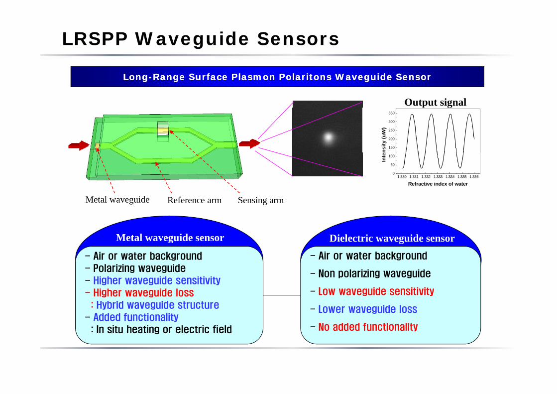
LRSPP Waveguide Sensors
LongLong--Range Surface Plasmon Polaritons Waveguide SensorRange Surface Plasmon Polaritons Waveguide Sensor
Output signal
150
200
250
300
350
nsity
(uW
)
p g
M t l id
1.330 1.331 1.332 1.333 1.334 1.335 1.3360
50
100
Inte
Refractive index of water
R f S iMetal waveguide Reference arm Sensing arm
Metal waveguide sensor Dielectric waveguide sensor
- Air or water background
- Polarizing waveguide
- Higher waveguide sensitivity
g e ec c w vegu de se so- Air or water background
- Non polarizing waveguide
- Higher waveguide loss
: Hybrid waveguide structure
- Added functionality
: In situ heating or electric field
- Low waveguide sensitivity
- Lower waveguide loss
- No added functionality: In situ heating or electric field y
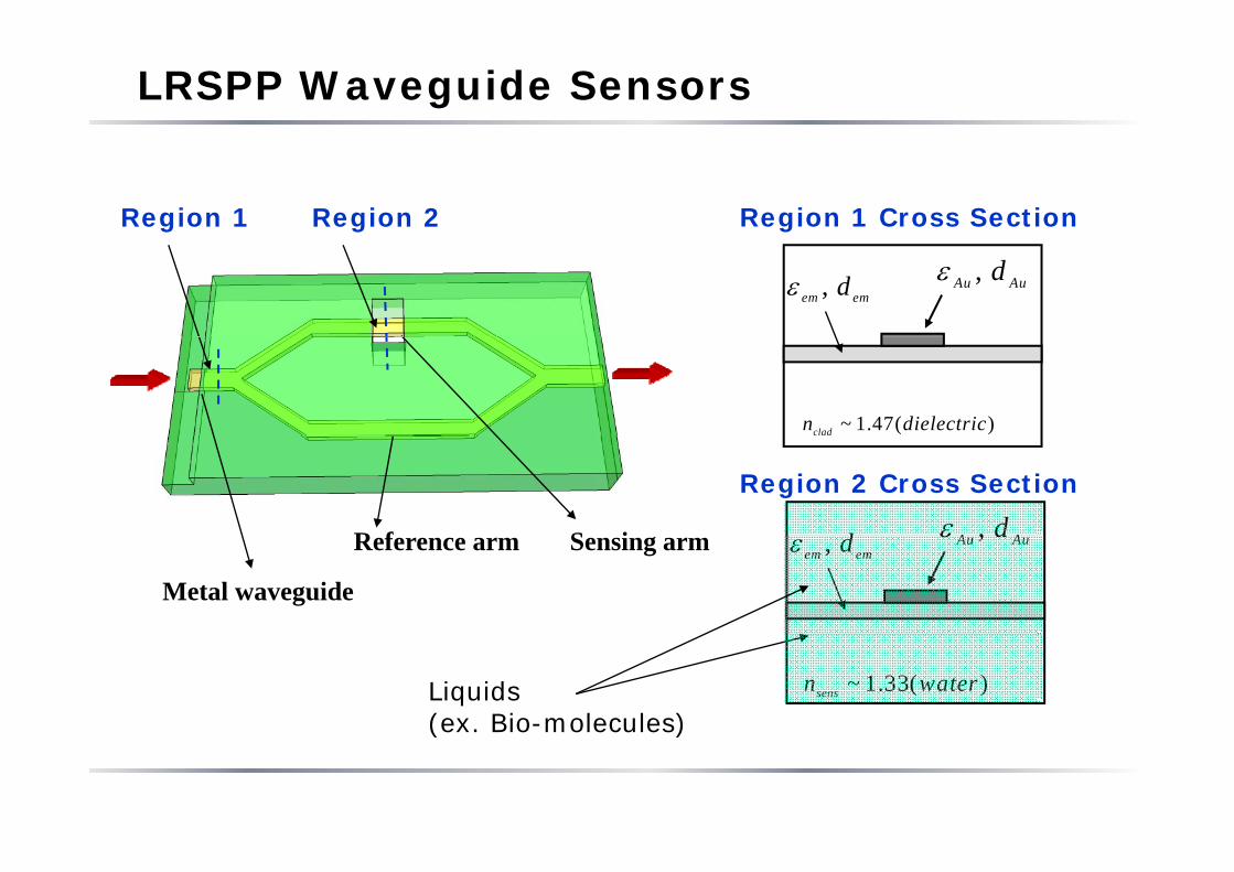
LRSPP Waveguide Sensors
Region 1 Region 2 Region 1 Cross Section
,em emdε ,Au Audε
~ 1.47( )cladn dielectric
R f S i
Region 2 Cross Section
d ,A Adε
Metal waveguide
Reference arm Sensing arm ,em emdε ,Au Audε
~ 1.33( )sensn waterLiquids(ex. Bio-molecules)( )
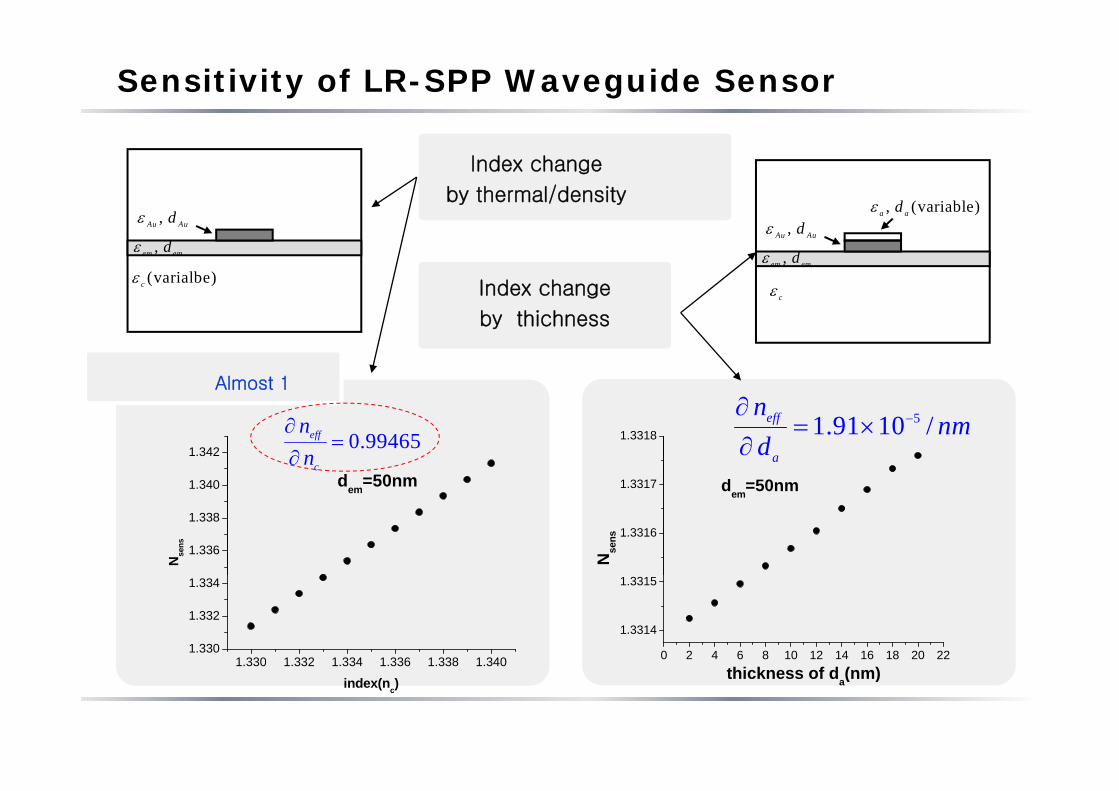
Sensitivity of LR-SPP Waveguide Sensor
, (variable)a adε
Index change
by thermal/densitydε
cε
,em emdε
,Au Audε
Index change(varialbe)cε
,em emdε
,Au Audε
by thichness
Almost 1
1 3317
1.3318
d =50nm1 340
1.342
d =50nm
51.91 10 /eff
a
nnm
d−∂
= ×∂0.99465eff
c
nn
∂=
∂
1.3316
1.3317 dem=50nm
Nse
ns
1.336
1.338
1.340 dem 50nm
Nse
ns
0 2 4 6 8 10 12 14 16 18 20 22
1.3314
1.3315
1.330 1.332 1.334 1.336 1.338 1.3401.330
1.332
1.334
thickness of da(nm)1.330 1.332 1.334 1.336 1.338 1.340
index(nc)
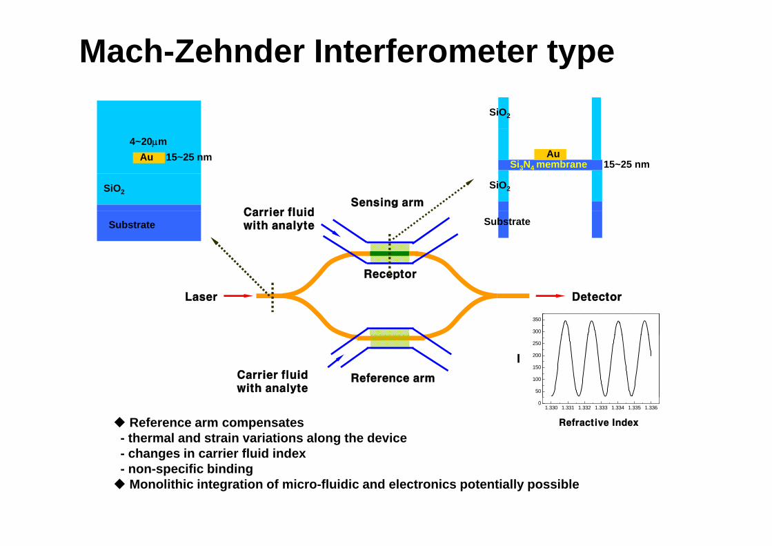
Mach-Zehnder Interferometer type
4~20μm
SiO2
Carrier fluidSensing arm
SiO2
Au 15~25 nm
SiO2
Au15~25 nmSi3N4 membrane
Receptor
Carrier fluid with analyteSubstrate Substrate
Laser Detector
Receptor
300
350
Carrier fluid with analyte
Reference arm50
100
150
200
250
Inte
nsity
(uW
)
I
Reference arm compensates- thermal and strain variations along the device- changes in carrier fluid index
1.330 1.331 1.332 1.333 1.334 1.335 1.3360
Refractive index of waterRefractive Index
g- non-specific binding
Monolithic integration of micro-fluidic and electronics potentially possible

MZI Sensor sensitivitySensing armSensing arm
L250
300
350
uW)
I
1.330 1.331 1.332 1.333 1.334 1.335 1.3360
50
100
150
200
Inte
nsity
(uI
0 2 3
Reference arm
Binding of bio-molecules on sensing armMode effective index change sensing arm
Refractive index of waterΔφ0 π 2π 3π
LneffΔ=Δ πφ 2
Mode effective index change sensing armMode propagation phase difference (Δφ) between sensing and reference arms
Phase difference is converted to intensity variation
( )( )⎥⎦⎤
⎢⎣⎡ +Δ+= 0cos121log10 φφI
Phase difference is converted to intensity variation
Sensitivity
Ca
an
nI
CIySensitivit eff
eff ∂∂
∂∂
∂∂
∂∂
=∂∂
=φ
φ
MZI 2πL/λ waveguide receptor

MZI-LRSPP Sensor Design1000 mμ
2
In Out40 mμ
1
1000 mμ 1000 mμ2000 mμ500 mμ 500 mμ 500 mμ 500 mμ
Cross section Cross section21 Metal
SiO2
5 mμ
20nm 100nmSiO2
Receptor
dielectric
dielectric
SiO2(1.47) Air(1.0)
SiO2
water metal
SiO2
membrane 1
substrate
membrane 2

Sensitivity
400
500
300
350
300
400
ity (u
W)
200
250
300
ty (u
W)
100
200
Inte
ns
50
100
150
Inte
nsit
0 10 20 30 40 500
Thickness of water (nm)1.330 1.331 1.332 1.333 1.334 1.335 1.336
0
Refractive index of water
If a detector has 0.1 uW sensitivity, 3 pm thickness variation can be detectable
If a detector has 0.1 uW sensitivity,3x10-7 index difference can be detecteddetectable. detected
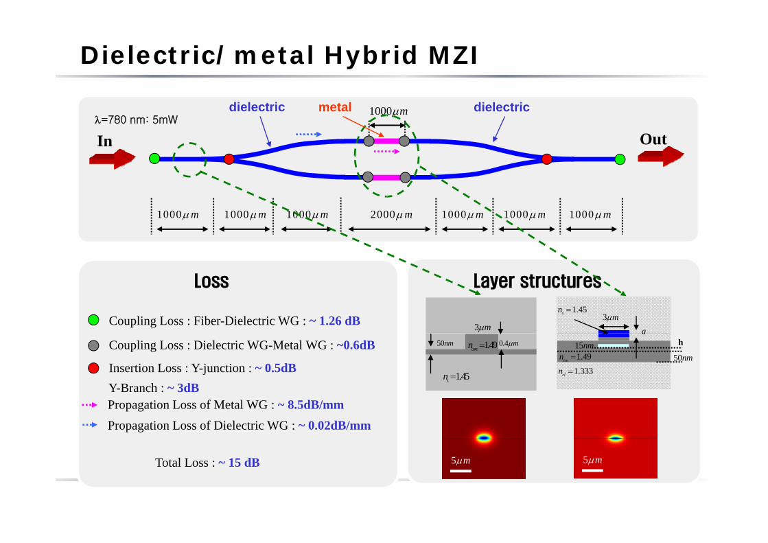
Dielectric/metal Hybrid MZI
1000 mμ
In Outλ=780 nm: 5mW
dielectric dielectricmetal
1000 mμ 1000 mμ2000 mμ1000 mμ 1000 mμ 1000 mμ 1000 mμ
Coupling Loss : Fiber-Dielectric WG : ~ 1.26 dB 3 mμ3 mμ
1.45sn =
a
Loss Layer structures
Insertion Loss : Y-junction : ~ 0.5dB
Coupling Loss : Dielectric WG-Metal WG : ~0.6dB
1.45sn =
1.49coren = 0.4 mμ50nm
50nm15nm
1.333cln =
1.49emn =
ha
Y-Branch : ~ 3dBPropagation Loss of Metal WG : ~ 8.5dB/mmPropagation Loss of Dielectric WG : ~ 0.02dB/mm
10 mμ510 mμ5 mμ5 mμTotal Loss : ~ 15 dB

Double-layered LRSPP waveguide type
Biocontents SAMcontents
Channelarea
Dielectric material
Cladding
Y Y Y Y Y Y Y Y Y Y Y Y Y Y Y Y Y Y Y Y
Y Y Y Y
< Double LR-SPP biosensor >
Metal (Au)Substrate
Cladding
Strip configurations
Mach-zender interferometers
Directional couplersDirectional couplers
DFB gratingsSubstrate
Bragg grating
y
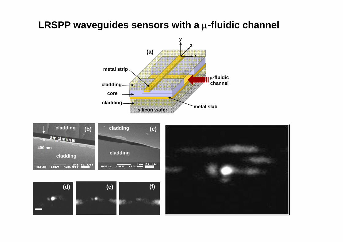
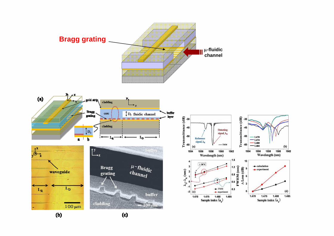
LRSPP waveguides sensors with a μ-fluidic channel
(a)
yz
x
μ-fluidicchannel
metal strip
core
cladding
silicon wafer
core
claddingmetal slab
450 nm
(b) (c)cladding cladding
450 nm
cladding cladding
(d) (e) (f)
Bragg gratingμ-fluidicchannel
Bragg grating
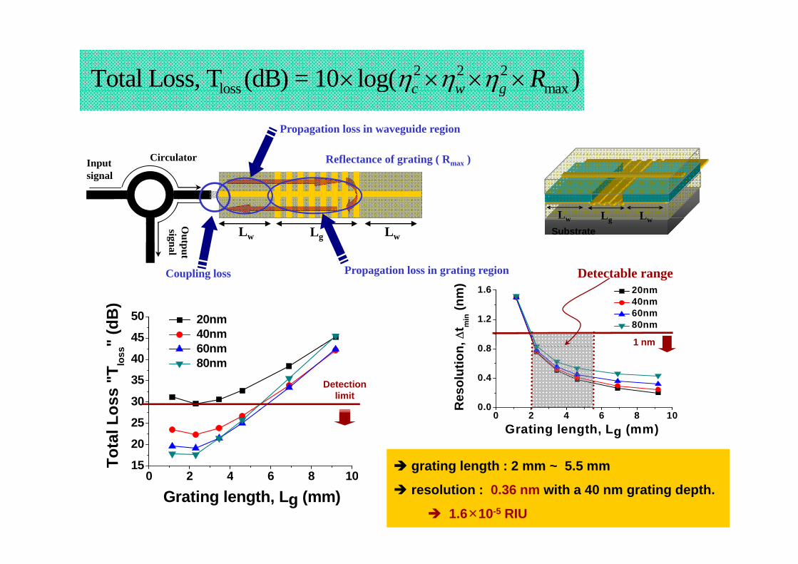
2 2 2loss maxTotal Loss, T (dB) = 10 log( )c w g Rη η η× × × ×
Ci l
loss max, ( ) g( )c w gη η η
Propagation loss in waveguide region
Lw LL
CirculatorInput signal
Reflectance of grating ( Rmax )
Lw LwLg
SubstrateLgLw Lw
Output
signal
Coupling loss Propagation loss in grating region Detectable range
45
50
" (d
B)
20nm 40nm60 0 8
1.2
1.6
, Δt m
in (n
m) 20nm
40nm 60nm 80nm
1 nm
30
35
40
oss
"Tlo
ss 60nm 80nm
Detectionlimit
0.0
0.4
0.8
Res
olut
ion
0 2 4 6 8 1015
20
25
Tota
l Lo 0 2 4 6 8 10
0 0
Grating length, Lg (mm)
grating length : 2 mm ~ 5.5 mm0 2 4 6 8 10
Grating length, Lg (mm) resolution : 0.36 nm with a 40 nm grating depth.
1.6×10⁻⁵ RIU
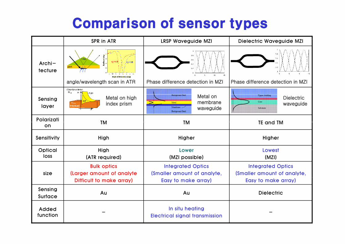
Comparison of sensor types SPR in ATR LRSP Waveguide MZI Dielectric Waveguide MZI
Archi-
tecture
angle/wavelength scan in ATR Phase difference detection in MZI Phase difference detection in MZI
Sensing
layer
PolarizatiTM TM TE and TM
Metal on high index prism
Metal on membrane waveguide
Dielectric waveguide
onTM TM TE and TM
Sensitivity High Higher Higher
Optical High Lower LowestOptical loss
High
(ATR required)
Lower
(MZI possible)
Lowest
(MZI)
size
Bulk optics
(Larger amount of analyte
Integrated Optics
(Smaller amount of analyte,
Integrated Optics
(Smaller amount of analyte,
Difficult to make array) Easy to make array) Easy to make array)
Sensing
SurfaceAu Au Dielectric
Added function
-In situ heating
Electrical signal transmission-
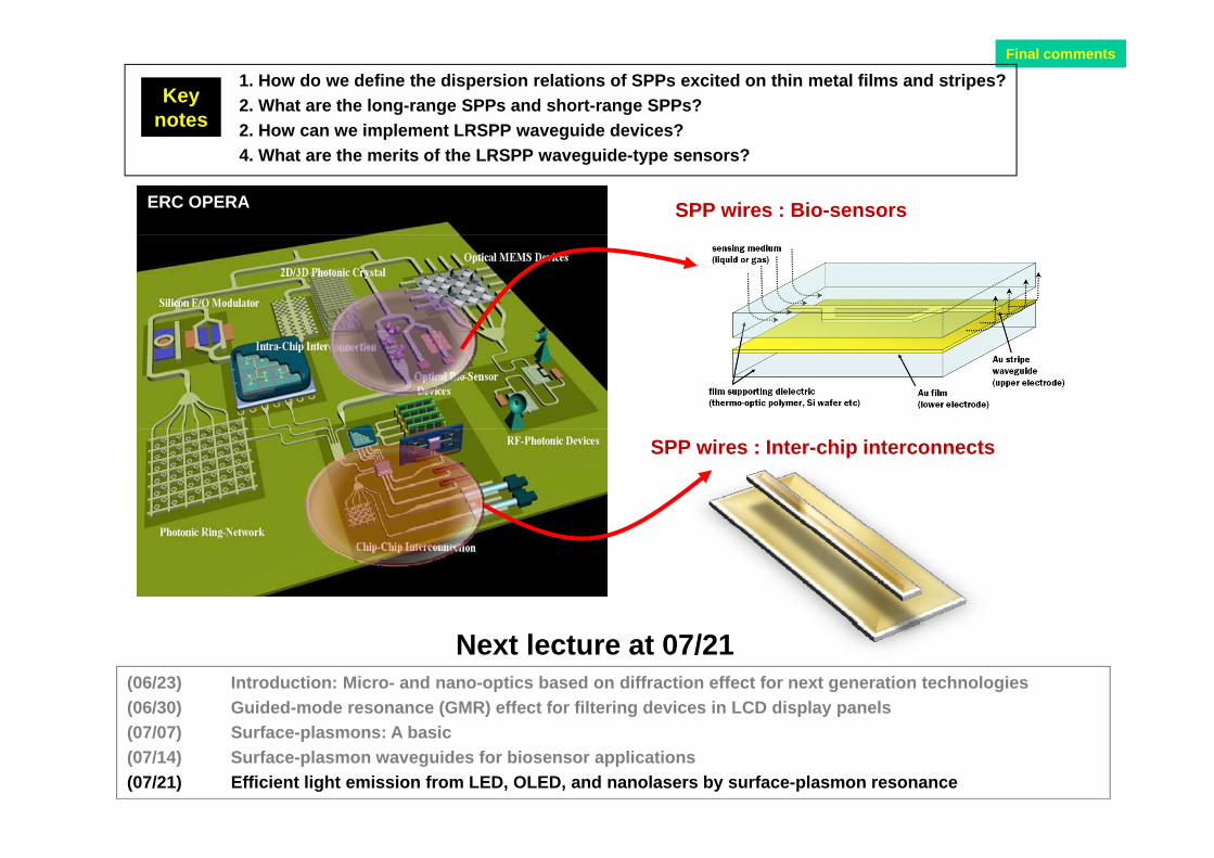
Final comments
1. How do we define the dispersion relations of SPPs excited on thin metal films and stripes?2. What are the long-range SPPs and short-range SPPs?2. How can we implement LRSPP waveguide devices?
Key notes
SPP wires : Bio-sensorsERC OPERA
p g4. What are the merits of the LRSPP waveguide-type sensors?
SPP wires : Inter-chip interconnects
Next lecture at 07/21(06/23) Introduction: Micro- and nano-optics based on diffraction effect for next generation technologies(06/30) Guided-mode resonance (GMR) effect for filtering devices in LCD display panels(07/07) Surface-plasmons: A basic(07/14) Surface-plasmon waveguides for biosensor applications(07/21) Efficient light emission from LED, OLED, and nanolasers by surface-plasmon resonance
(Appendix) GMR grating sensors(Appendix) GMR grating sensors
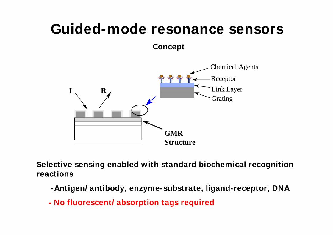
Guided-mode resonance sensorsConcept
I R Link LayerReceptor
Chemical Agents
I RGrating Link Layer
GMR Structure
Selective sensing enabled with standard biochemical recognition i
Structure
reactions
-Antigen/antibody, enzyme-substrate, ligand-receptor, DNA
- No fluorescent/absorption tags required
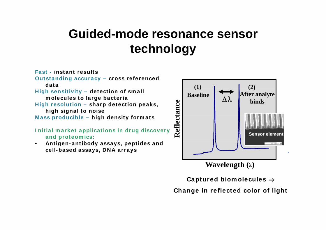
Guided-mode resonance sensorGuided mode resonance sensor technology
Fast - instant resultsOutstanding accuracy – cross referenced
data (1) (2)High sensitivity – detection of small
molecules to large bacteriaHigh resolution – sharp detection peaks,
high signal to noise
( )Baseline
(2) After analyte
bindsΔλ
tanc
e
Mass producible – high density formats
Initial market applications in drug discovery and proteomics:
i ib d id d
Ref
lect
Sensor element
• Antigen-antibody assays, peptides and cell-based assays, DNA arrays
Wavelength (λ)
Captured biomolecules ⇒
Change in reflected color of light
g ( )
g g
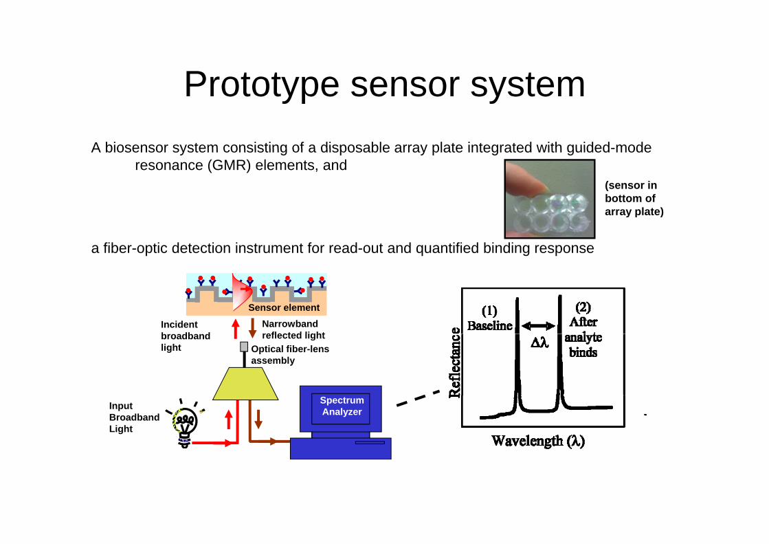
Prototype sensor systemPrototype sensor systemA biosensor system consisting of a disposable array plate integrated with guided-modeA biosensor system consisting of a disposable array plate integrated with guided-mode
resonance (GMR) elements, and(sensor in bottom of array plate)
a fiber-optic detection instrument for read-out and quantified binding response
array plate)
Incident b db d
Narrowbandreflected light
Sensor element
Optical fiber-lens assembly
broadband light
reflected light
SpectrumAnalyzerInput
Broadband Light
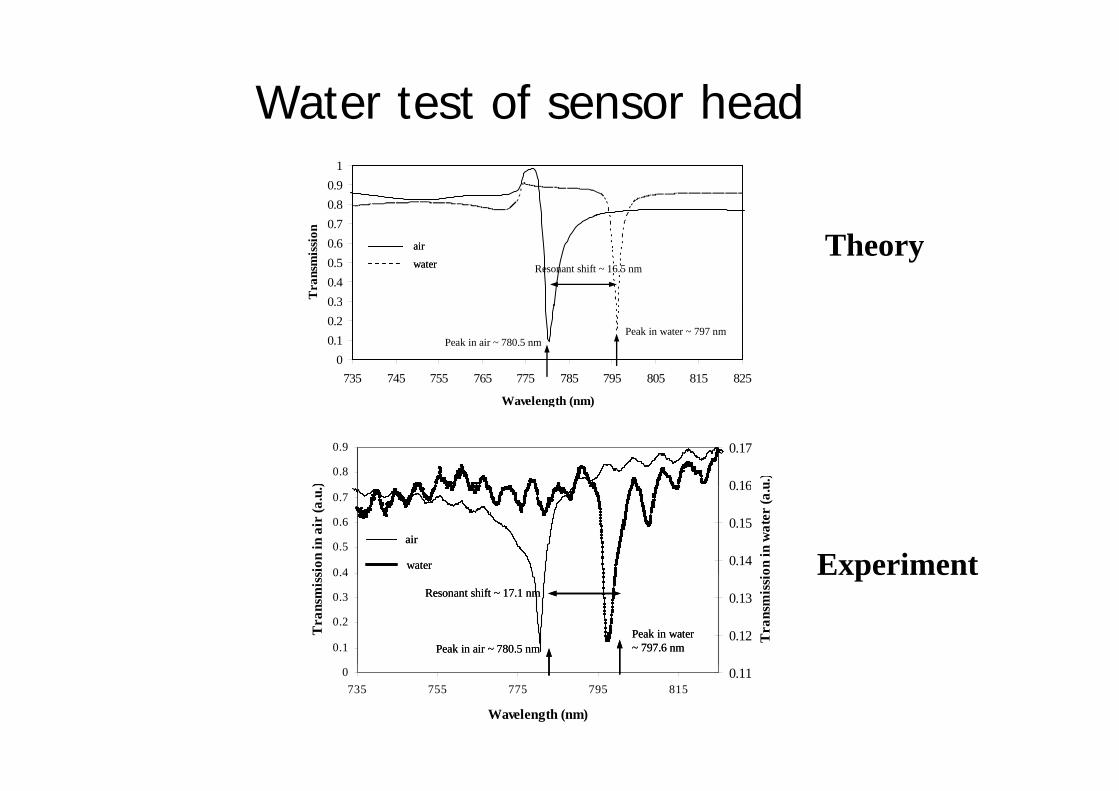
Water test of sensor head
0.80.9
1
0.80.9
1
0.30.40.50.60.7
Tra
nsm
issi
on
Resonant shift ~ 16.5 nm
air
water
0.30.40.50.60.7
Tra
nsm
issi
on
Resonant shift ~ 16.5 nm
air
water
air
waterTheory
00.10.20.3
735 745 755 765 775 785 795 805 815 825
Peak in water ~ 797 nmPeak in air ~ 780.5 nm
00.10.20.3
735 745 755 765 775 785 795 805 815 825
Peak in water ~ 797 nmPeak in air ~ 780.5 nm
Wavelength (nm)Wavelength (nm)
0.8
0.9
) 0 16
0.17
u.)0.8
0.9
) 0 16
0.17
u.)
0.4
0.5
0.6
0.7
sion
in a
ir (a
.u.)
0.14
0.15
0.16
on in
wat
er (a
.u
air
water0.4
0.5
0.6
0.7
sion
in a
ir (a
.u.)
0.14
0.15
0.16
on in
wat
er (a
.u
air
water
air
water Experiment
0.1
0.2
0.3
0.4
Tra
nsm
iss
0.12
0.13
Tra
nsm
issi
Peak in water ~ 797.6 nmPeak in air ~ 780.5 nm
Resonant shift ~ 17.1 nm
0.1
0.2
0.3
0.4
Tra
nsm
iss
0.12
0.13
Tra
nsm
issi
Peak in water ~ 797.6 nmPeak in air ~ 780.5 nm
Resonant shift ~ 17.1 nm
Peak in water ~ 797.6 nmPeak in air ~ 780.5 nm
Resonant shift ~ 17.1 nm
pe e
0735 755 775 795 815
Wavelength (nm)
0.110735 755 775 795 815
Wavelength (nm)
0.11

B t i l tt h t hBacterial attachment scheme
Blocking protein
Antibody
S. aureus bacteria (1 μm)
Silane layer xxxGrating element
P Sil t d ti f bi d tib di th t tt h t t i A ( f t i SProcess: Silane-coated grating surface binds antibodies that attach to protein A (surface protein on S. aureusbacteria). Milk protein added to block nonspecific binding of S. aureus to unoccupied silane sites.
Chemistry steps provided in Magnusson et al, Proc SPIE vol. 6008, pp. 60080U 1-10, 2005.
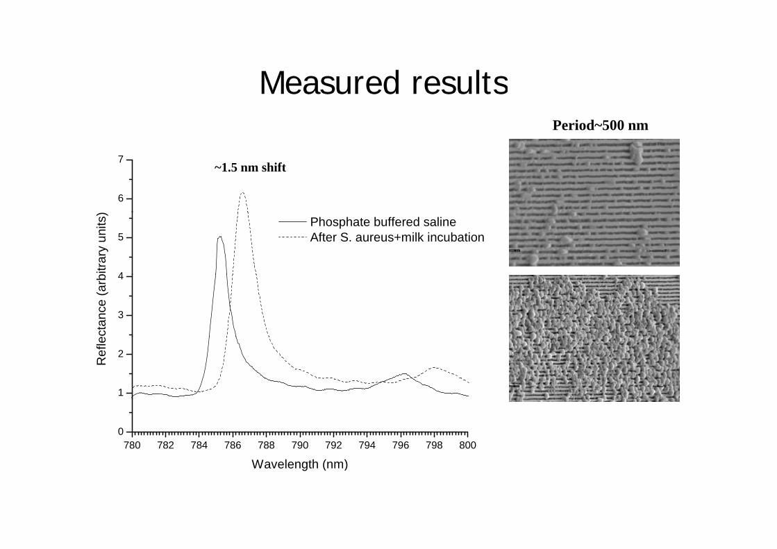
Measured resultsMeasured resultsPeriod~500 nm
6
7~1.5 nm shift
4
5
bitra
ry u
nits
)
Phosphate buffered saline After S. aureus+milk incubation
3
4
ecta
nce
(arb
1
2
Ref
le
780 782 784 786 788 790 792 794 796 798 8000
W l th ( )Wavelength (nm)
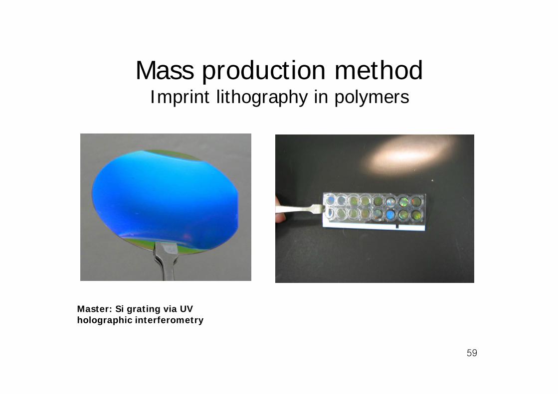
M d ti th dMass production methodImprint lithography in polymers
Master: Si grating via UV holographic interferometry
59

Next generation: Integrated GMR biochipsAngular addressing, laser source, transmission
Microwell plates
Platform holding an NxM detector matrix
GMR Sensor
Microlens Array
Plane Wave
Estimated density~100x100 elements/cm2
60