susbtrate-induced stabilization and reconstruction of zigzag edges
TRANSCRIPT

arX
iv:1
502.
0077
1v1
[con
d-m
at.m
trl-s
ci]
3 F
eb 2
015 Substrate-Induced Stabilization and Reconstruction
of Zigzag Edges in Graphene Nanoislands on Ni(111)
A. Garcia-Lekue,∗,†,‡ M. Ollé,∗,¶,§ D. Sanchez-Portal,†,‖ J.J. Palacios,⊥,# A.
Mugarza,¶ G. Ceballos,¶ and P. Gambardella¶,§,@
Donostia International Physics Center (DIPC), Paseo Manuel de Lardizabal 4, E-20018 San
Sebastián, Spain, IKERBASQUE, Basque Foundation for Science, E-48011, Bilbao, Spain,
Catalan Institute of Nanoscience and Nanotechnology (ICN2), UAB Campus, E-08193 Bellaterra
(Barcelona), Spain, Department of Materials, Eidgenössische Technische Hochschule (ETH)
Zurich, Hönggerbergring 64, CH-8093 Zurich, Switzerland, Centro de Física de Materiales
CSIC-UPV/EHU, Paseo Manuel de Lardizabal 5, San Sebastián, Spain, Departamento de Física
de la Materia Condensada, Universidad Autónoma de Madrid, Cantoblanco, Madrid 28049,
Spain, Instituto de Física de la Materia Condensada (IFIMAC), Universidad Autónoma de
Madrid, Cantoblanco, Madrid 28049, Spain, and Institució Catalana de Recerca i Estudis
Avancats (ICREA), E-08193 Barcelona, Spain
E-mail: [email protected]; [email protected]
Abstract∗To whom correspondence should be addressed†Donostia International Physics Center (DIPC)‡IKERBASQUE, Basque Foundation for Science, E-48011, Bilbao, Spain¶Catalan Institute of Nanoscience and Nanotechnology (ICN2)§Eidgenössische Technische Hochschule (ETH) Zurich‖Centro de Física de Materiales CSIC-UPV/EHU (CFM)⊥Dpto. de Física de la Materia Condensada, Univ. Autónoma de Madrid#Instituto de Física de la Materia Condensada (IFIMAC), Univ. Autónoma de Madrid
@Institució Catalana de Recerca i Estudis Avancats (ICREA)
1

We combine experimental observations by scanning tunneling microscopy (STM) and den-
sity functional theory (DFT) to reveal the most stable edge structures of graphene on Ni(111)
as well as the role of stacking-driven activation and suppression of edge reconstruction. De-
pending on the position of the outermost carbon atoms relative to hollow and on-top Ni sites,
zigzag edges have very different energies. Triangular graphene nanoislands are exclusively
bound by the more stable zigzag hollow edges. In hexagonal nanoislands, which are con-
strained by geometry to alternate zigzag hollow and zigzag top edges along their perimeter,
only the hollow edge is stable whereas the top edges spontaneously reconstruct into the (57)
pentagon-heptagon structure. Atomically-resolved STM images are consistent with either top-
fcc or top-hcp epitaxial stacking of graphene and Ni sites, with the former being favored by
DFT. Finally, we find that there is a one-to-one relationshipbetween the edge type, graphene
stacking, and orientation of the graphene islands.
Introduction
Edges play a fundamental role in shaping the morphology1–5 and electronic6–9 properties of
graphene nanostructures. Electron confinement due to edge boundaries gives rise to energy band
gaps,10,11 localized states6,7, spin-polarization,10,12and spin-dependent electron scattering.13 Fur-
thermore, graphene edges determine the preferred sites forthe attachment of metal atoms,14 chem-
ical functionalization,15 as well as oxygen etching and intercalation.16,17Understanding and defin-
ing the edge morphology is therefore important to tune the growth of graphene nanostructures as
well as to modulate the electronic properties of graphene inconfined geometries.
In free-standing graphene, crystallographically oriented edges are of either zigzag (zz) or arm-
chair (ac) type.6 Graphene with ac and zz edges can be obtained by mechanical exfoliation18 and
etching techniques.19 However, free-standing unpassivated edges are unstable due to the high den-
sity of dangling bonds,20–22 which induce the zz edges to spontaneously reconstruct intoa line
of pentagon and heptagon pairs, the so called zz(57) or Stone-Wales reconstruction.23,24. A very
different scenario arises in epitaxially grown graphene, where the interaction with the substrate
2

can stabilize ac,25,26zz,27–29and reconstructed edges,4,30–32and induce complex graphene-metal
boundaries.28,29,33
Despite the potential of epitaxy for tailoring graphene edges evidenced by these studies, pre-
dicting the edge structure is still a challenging task, which requires detailed insight into the inter-
play of substrate interaction and edge morphology. For example, minimal variations in the lattice
constant and electronic structure of the substrate can leadto very different edge energetics, re-
sulting in hexagonal islands with zz and Klein-type edges inCo(1000),30 and either hexagonal or
triangular islands in Ni(111), depending on growth parameters.34,35The latter strongly differ from
the quasi-isotropic shape predicted by theory.4,31
In this work, we show that the experimentally observed morphological transition of graphene
islands on Ni(111) is driven by a substrate-induced reconstruction of zz edges into the zz(57) struc-
ture.This reconstruction, which was found to be unstable onmost close-packed metals including
Ni(111) according to previous first principles calculations,4,31, occurs along a particular direction
with respect to the substrate, and can only be properly reproduced by theory by taking into account
the stacking of differently oriented edges.
Methods
Experiments
Graphene nanoislands were grown on a Ni(111) single-crystal surface kept in a ultra-high vacuum
(UHV) chamber with a base pressure of 3×10⁻¹⁰ mbar. The crystal surface was cleaned by re-
peated cycles of Ar+ sputtering followed by annealing at 800◦C during 1 minute. The surface tem-
perature was measured throughout the experiment using a pyrometer (IMPAC IGA 140). Propene
was dosed on a freshly prepared Ni(111) crystal at room temperature. Once the dosing process
is complete the sample is heated at 500◦C for 5 minutes to nucleate the graphene nanoislands
and subsequently cooled to room temperature. The islands soobtained have an irregular shape. In
order to prepare triangular and hexagonal graphene islands(TGIs and HGIs, respectively) we post-
3
anneal the sample to a temperatureTA = 500◦C (650◦C) during a timetA = 20 min (10 min). We
use a propene doseD= 1 L for the TGIs andD= 2 L for the HGIs to compensate for C loss at high
temperature. The heating rate was 12◦C/s and the cooling rate was 1.7◦C/s. It should be empha-
sized that the presence of contaminants, such as H or CO, is minimized by annealing the samples
in UHV. Atomic H as well as molecular species, such as CO, desorb from Ni(111) at temperatures
lower than 300◦C.36,37 Moreover, we observe that the island shape does not change at500◦C,
which is another indication that the edge structures are notdriven by hydrogenation. Although
it is notoriously difficult to completely rule out the presence of contaminants, the fact that DFT
calculations provide a very satisfactory explanation for the STM observations can be considered
as a further evidence for the absence of contaminants at the edges. More details on the preparation
of the TGIs and HGIs preparation can be found in Ref. 35. Topographic images of the surface
were obtained at room temperature using a variable-temperature scanning tunneling microscope
(SPECS, STM Aarhus 150) and processed using a freeware software (WSxM 5.0 develop 4.1).38
Theory
Ab-initio spin-polarized calculations were performed using DFT as implemented in the SIESTA39
and ANT.G codes.40 For the description of TGIs using SIESTA, we considered a supercell made
of a three Ni(111) layers (up to four layers in convergence test, see the Supporting Information)
and one graphene island containing 22 C atoms, whereas the results using ANT.G were obtained
employing a graphene island of 33 C atoms placed on a Ni(111) surface described by a cluster with
2 Ni layers. The simulation of HGIs with alternate edge typeswould require the use of extremely
large supercells; we have therefore used the nanoribbon geometry to compare the properties of
different graphene edges on Ni(111) using SIESTA. The results obtained for the nanoribbon cal-
culations yield information on the edge stability and energetics, which can be extended to the case
of large hexagonal nanoislands. For such calculations we employed a 4x8 supercell made of three
Ni(111) layers and a graphene ribbon containing 40 C atoms placed on one of the surfaces. In this
case, only graphene nanoribbons with top-fcc stacking withrespect to the underlying Ni(111) were
4

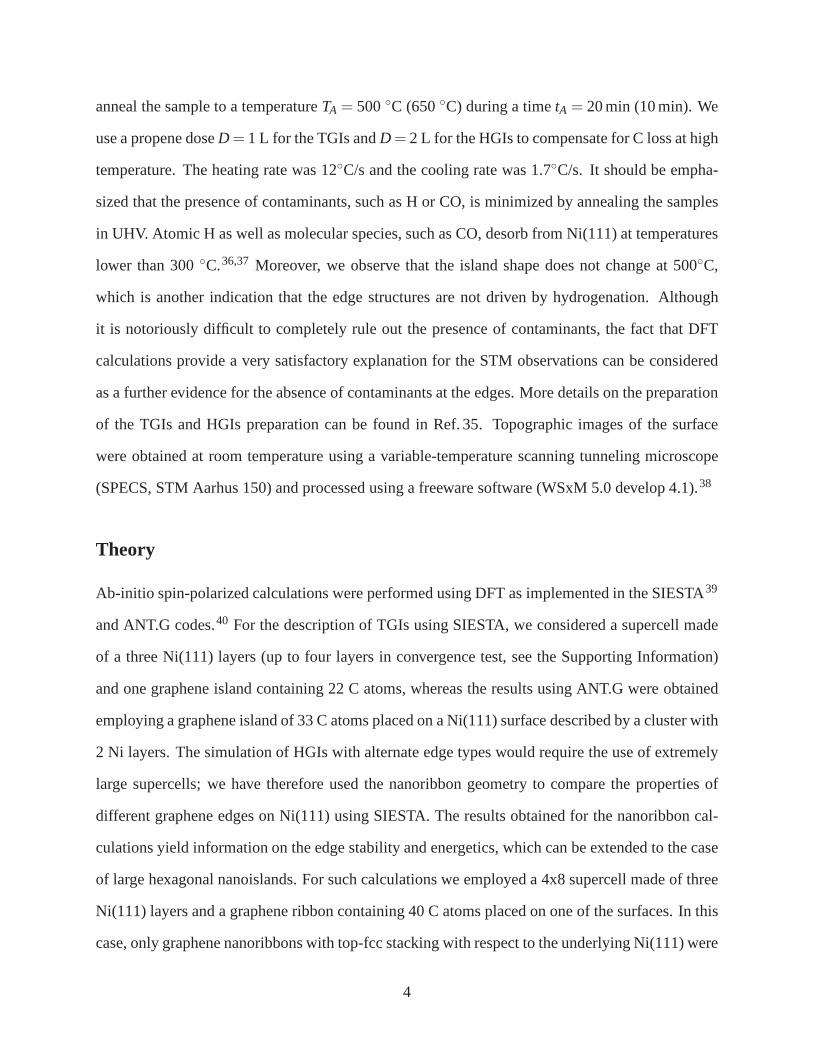
Figure 1: Hard sphere models of different zigzag graphene edges on Ni(111) for fcc (left) and hcp(right) graphene-Ni stacking.
considered. Further details on the calculations are given in the Supporting Information.
Results and discussion
The small lattice mismatch between graphene and Ni(111), 1×1 stacking, and the corresponding
absence of a Moiré pattern make this system an optimal candidate to investigate the structure,
stability, and epitaxial relationship between the graphene edges and a metallic substrate. Several
1×1 stacking structures have been proposed for graphene monolayers on Ni(111).41–45According
to these previous studies, the top-fcc, top-hcp and bridge-top configurations are considered to be
the most stable, with a small energetic preference for the top-fcc stacking. Indeed, a recent report
has confirmed the coexistance of these three graphene configurations on Ni(111), with a general
5
predominance of top-fcc.46 In the case of graphene nanoislands on Ni(111) reported here, the
possible stacking configurations are expected to be the sameas for the graphene monolayer. Sym-
metry arguments, however, allow us to exclude bridge-top stacking (see Supporting Information)
and consider only top-fcc and top-hcp stacking shown in Figure 1.
Regarding zz edges, we distinguish two different types according to the position of the outer-
most C atoms with respect to the substrate. We thus define edges having the outer C atoms located
on top of Ni atoms as zzt and edges having the outer C atoms on hollow sites as zzh, as shown in
Figure 1. The outer C atoms of a zzh edge can occupy hollow fcc or hcp sites, depending on the
stacking configuration and edge orientation. As seen in Figure 1, the crystallographic directions of
zzt and zzh edges with the same stacking differ by 60◦ and the crystallographic directions of edges
of the same type but different stacking also differ by 60◦. Note also that an edge perpendicular to
the (121) direction can be either a top-fcc/zzt or a top-hcp/zzh edge, while an edge perpendicular
to the (112) direction can be either a top-fcc/zzh or a top-hcp/zzt edge.
In previous work, we have shown that graphene islands that nucleate with random shape upon
dosing propene on a clean Ni(111) surface and annealing the substrate above 450◦C evolve to
either triangular or hexagonal shapes depending on the initial hydrocarbon dose, annealing time,
and temperature.35 Such TGIs and HGIs provide an ideal system to study the structure and stacking
of the edge C atoms on close-packed metal surfaces. Due to thethreefold symmetry of the zzt and
zzh edges introduced above, TGIs present only a single edge typewhereas HGIs must alternate
different edges. By varying the island size and shape it is thus possible not only to characterize the
different edges but also to study the influence of the edge morphology and graphene stacking on
the stability of the islands.
Figure 2(a) shows a representative STM image of TGIs obtained by annealing the substrate
to 500◦C and subsequent cooling to room temperature (see Methods).Under these conditions,
most islands exhibit straight edges, which indicates that they can only be of either zz or ac type.
Topographic images with atomic resolution on both grapheneand Ni are shown in Figure 2(b)
and (c). We observe that the TGIs have unreconstructed zz edges with no defects, in agreement
6

with previous results.34,35The edge shown in Figure 2(c) runs perpendicular to the [112] direction,
i.e., parallel to a high symmetry [110] direction of the Ni lattice. A honeycomb and an hexago-
nal lattice, representing the atomic positions of the graphene and surface Ni atoms respectively,
have been superposed on the image for illustrative purposes. Note that the STM image taken over
the graphene-covered region exhibits almost hexagonal contrast, despite the honeycomb atomic
structure of graphene. This is a well-known electronic effect induced by the graphene-metal in-
teraction, which breaks the symmetry between C atoms in on-top and hollow positions.46–48 In
particular, previous theoretical simulations concluded that in the case of graphene on Ni(111) the
bright spots in the STM images at zero or very small bias correspond to C atoms located in hollow
positions,46,47as reproduced also by our calculations. Besides, all the images shown in this work
have been acquired under well controlled tip conditions, which allows us to exclude tip-induced
contrast effects. All this suggests that, away from local variations related, e.g., to surface impu-
rities, lattice imperfections, and the proximity of the edge, the spots with larger intensity in the
STM images correlate with C atoms in hollow positions. In anycase, the hexagonal units of the
honeycomb lattice can be clearly identified and extrapolated to the Ni lattice, which let us draw
two important conclusions: i) that vertices of the honeycomb lattice at the graphene-Ni lateral
boundary (red circles) correspond to hollow positions on the hexagonal lattice, and hence the edge
is of zzh type; ii) The vertices representing the other sublattice (blue circles) are located on top
of the Ni atoms, and hence graphene has either top-fcc or top-hcp stacking with the substrate, in
agreement with our initial hypothesis.
The great majority of the TGIs in our samples point in the samedirection, as seen in Figure 2(a).
Because there is a one-to-one relationship between the edgetype, stacking, and orientation of TGIs
(Figure S2 of the Supporting Information), this implies that the TGIs have a preference for a unique
edge type and stacking combination, which, according to ouranalysis, corresponds to zzh and
either top-fcc or top-hcp. Moreover, we find evidence that the edge type dominates the preference
for the epitaxial stacking of the inner C atoms in the islands. The enlarged area of Figure 2(a)
shows two TGIs pointing in opposite directions, meaning that they are rotated with respect to each
7
other by 60◦. This inverted orientation can only be explained by a changein the stacking or in
the edge type (see Figure S2 of the Supporting Information).Note that all the TGIs pointing in
the direction opposite to the predominant one [indicated byarrows in Figure 2(a)] have a small
size, below 10 nm2. Since the effect of the edge type on the system’s energy is higher for smaller
islands, the most plausible scenario is that the TGIs with inverted orientation maintain the lowest
energy edge configuration and change their stacking.
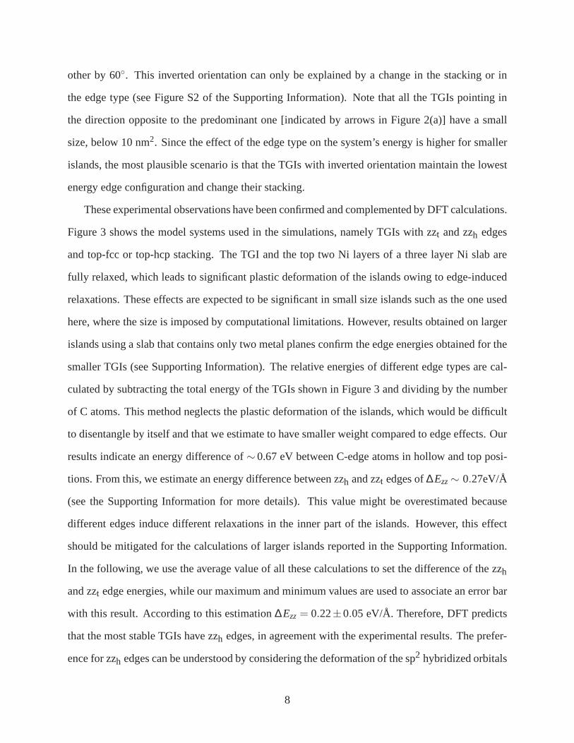
These experimental observations have been confirmed and complemented by DFT calculations.
Figure 3 shows the model systems used in the simulations, namely TGIs with zzt and zzh edges
and top-fcc or top-hcp stacking. The TGI and the top two Ni layers of a three layer Ni slab are
fully relaxed, which leads to significant plastic deformation of the islands owing to edge-induced
relaxations. These effects are expected to be significant insmall size islands such as the one used
here, where the size is imposed by computational limitations. However, results obtained on larger
islands using a slab that contains only two metal planes confirm the edge energies obtained for the
smaller TGIs (see Supporting Information). The relative energies of different edge types are cal-
culated by subtracting the total energy of the TGIs shown in Figure 3 and dividing by the number
of C atoms. This method neglects the plastic deformation of the islands, which would be difficult
to disentangle by itself and that we estimate to have smallerweight compared to edge effects. Our
results indicate an energy difference of∼0.67 eV between C-edge atoms in hollow and top posi-
tions. From this, we estimate an energy difference between zzh and zzt edges of∆Ezz∼ 0.27eV/Å
(see the Supporting Information for more details). This value might be overestimated because
different edges induce different relaxations in the inner part of the islands. However, this effect
should be mitigated for the calculations of larger islands reported in the Supporting Information.
In the following, we use the average value of all these calculations to set the difference of the zzh
and zzt edge energies, while our maximum and minimum values are usedto associate an error bar
with this result. According to this estimation∆Ezz= 0.22±0.05 eV/Å. Therefore, DFT predicts
that the most stable TGIs have zzh edges, in agreement with the experimental results. The prefer-
ence for zzh edges can be understood by considering the deformation of the sp2 hybridized orbitals
8

of the edge C atoms as they bind to the surface Ni atoms. In the case of zzh edges only a small
deformation is required to form a bond with a Ni atom, whereasfor zzt edges a larger deformation
takes place, which also leads to the bent edge structure thatcan be observed in Figure 3.
With respect to the stacking with the substrate, the calculations predict a small energy gain for
the top-fcc stacking with respect to the top-hcp, of the order of a few tens of meV per C atom,
which is not very significant in the case of the small islands considered in this study. This result
agrees with the calculations for extended graphene on Ni(111).43 Moreover, it is consistent with
the preferential orientation found for the TGIs. The small energy difference obtained for the two
stacking configurations is reflected by the fact that islandswith opposite orientation, although very
rare, can still be observed when their size is small enough [Figure 2(a)].
Figure 4(a) shows that TGIs evolve into HGIs by annealing theNi(111) surface up to 650◦C
for 10 minutes. This seems to imply that the growth of the TGIsis kinetically limited, whereas
the equilibrium shape of the graphene islands on Ni(111) is hexagonal, as confirmed by the re-
sults of our DFT simulations. This is similar to the homo- andhetero-epitaxy of metals on (111)
surfaces.49,50 The triangular and hexagonal island shapes allow us to compare the structure and
stability of different edge types. Contrary to TGIs, HGIs are constrained to exhibit zzh and zzt
edges alternated along their perimeter. Because of the 60◦ angle between adjacent edges, the for-
mation of ac edges can be excluded since these would be oriented at 30◦ with respect to the zz
edges. As in the case of TGIs, HGIs have their edges aligned with the high symmetry directions of
the substrate, and hence possess only zz edges. Since zzh and zzt edges alternate independently of
the stacking (Figure 1), the edge energy contribution is equivalent for top-fcc and top-hcp stack-
ing. The orientation of the islands does not change as they evolve from triangular to hexagonal
by increasing the annealing temperature from 500◦C to 650◦C, which indicates that the prefer-
ential stacking for the HGIs and TGIs is the same, that is, top-fcc according to the DFT results.
Figure 4(b) shows a detail of an HGI. Edges 1, 3, and 5 appear atomically straight and correspond
to zzh edges. Edges 2, 4 and 6, on the other hand, present a few structural imperfections and are
shorter compared to the odd-numbered edges. These edges should be of the zzt type according
9
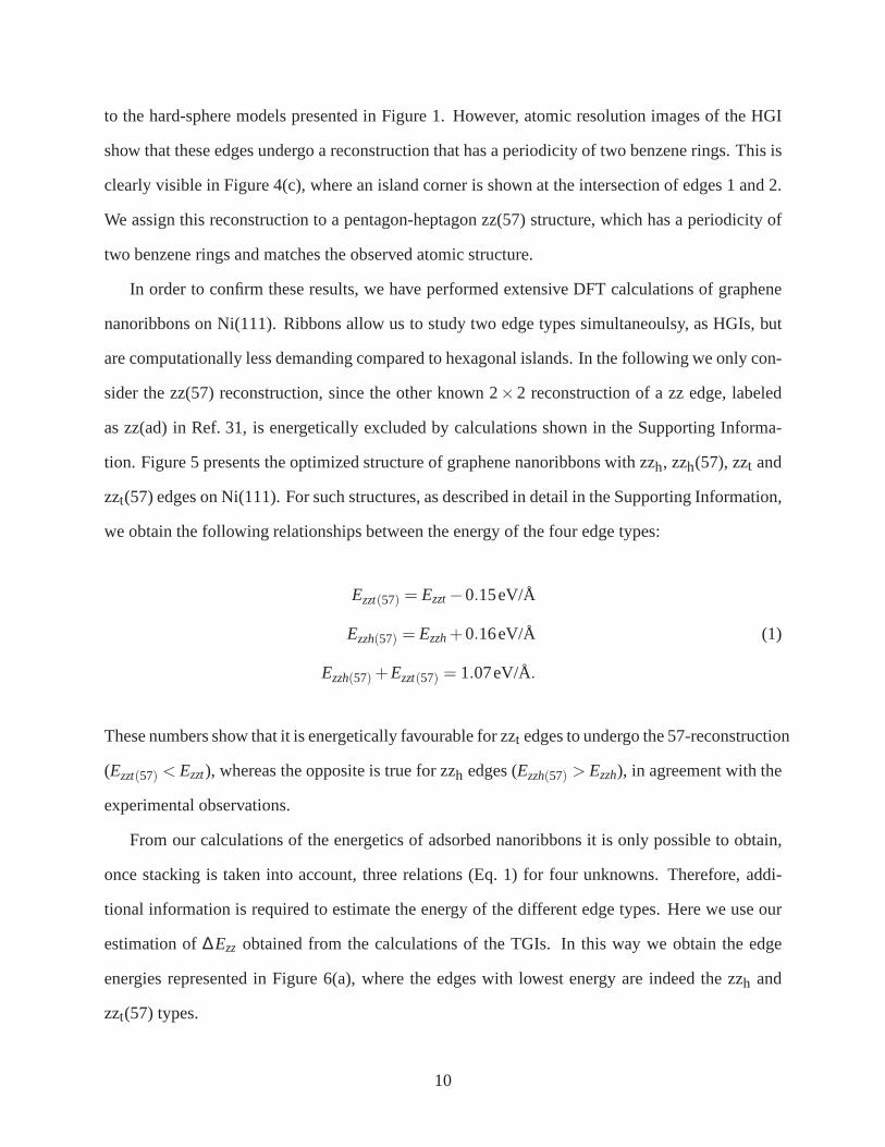
to the hard-sphere models presented in Figure 1. However, atomic resolution images of the HGI
show that these edges undergo a reconstruction that has a periodicity of two benzene rings. This is
clearly visible in Figure 4(c), where an island corner is shown at the intersection of edges 1 and 2.
We assign this reconstruction to a pentagon-heptagon zz(57) structure, which has a periodicity of
two benzene rings and matches the observed atomic structure.
In order to confirm these results, we have performed extensive DFT calculations of graphene
nanoribbons on Ni(111). Ribbons allow us to study two edge types simultaneoulsy, as HGIs, but
are computationally less demanding compared to hexagonal islands. In the following we only con-
sider the zz(57) reconstruction, since the other known 2×2 reconstruction of a zz edge, labeled
as zz(ad) in Ref. 31, is energetically excluded by calculations shown in the Supporting Informa-
tion. Figure 5 presents the optimized structure of graphenenanoribbons with zzh, zzh(57), zzt and
zzt(57) edges on Ni(111). For such structures, as described in detail in the Supporting Information,
we obtain the following relationships between the energy ofthe four edge types:
Ezzt(57) = Ezzt−0.15eV/Å
Ezzh(57) = Ezzh+0.16eV/Å (1)
Ezzh(57)+Ezzt(57) = 1.07eV/Å.
These numbers show that it is energetically favourable for zzt edges to undergo the 57-reconstruction
(Ezzt(57) < Ezzt), whereas the opposite is true for zzh edges (Ezzh(57) > Ezzh), in agreement with the
experimental observations.
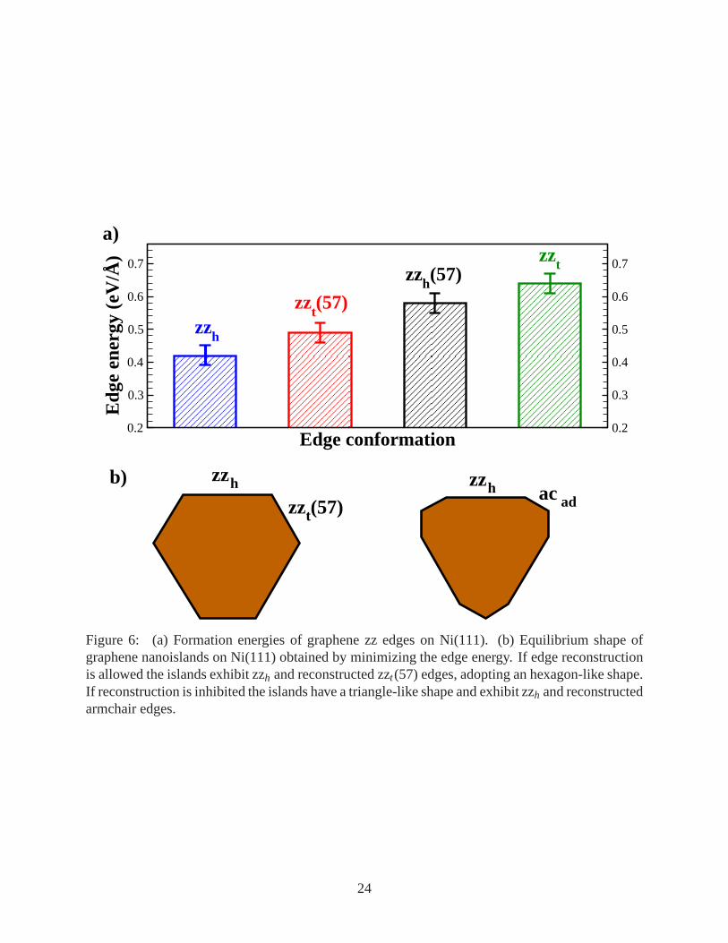
From our calculations of the energetics of adsorbed nanoribbons it is only possible to obtain,
once stacking is taken into account, three relations (Eq. 1)for four unknowns. Therefore, addi-
tional information is required to estimate the energy of thedifferent edge types. Here we use our
estimation of∆Ezz obtained from the calculations of the TGIs. In this way we obtain the edge
energies represented in Figure 6(a), where the edges with lowest energy are indeed the zzh and
zzt(57) types.
10

The results of our calculations are in disagreement with recent theoretical studies of graphene
nanoribbons on Ni(111),4,31 in which the unreconstructed edge is predicted to be more stable than
the reconstructed one. However, these studies do not consider the influence of stacking, which
leads to the conclusion that the 57-reconstructed edges arealways less stable than the unrecon-
structed ones. Besides, at least in one of these works,4 the estimation of the edge formation
energies is based on the assumption that the ribbons are perfectly symmetric, which is not true
if epitaxial stacking is taken into account (see Figure S4 ofthe Supporting Information). However,
it is interesting to note that the average value (over the twostacking configurations) of our edge
energies is in good agreement with the values reported by Gaoet al.31 using plane-wave calcula-
tions and the same exchange-correlation functional that weuse here (Perdew, Burke and Ernzerhof
functional51, see the Supporting Information). The agreement is particularly good for the unrecon-
structed zigzag edges, for which our average edge energy is 0.53 eV/Å, exactly the value reported
by Gaoet al. for the zigzag edge energy (without resolving the stacking dependency). Our average
value for the 57-reconstructed edge energies is∼0.54 eV/Å, which is somewhat lower than the
0.60 eV/Å reported by Gaoet al., but still in good correspondence.
With the edge energies in Figure 6(a), following the classical Wulff construction, the equilib-
rium shape of graphene islands on Ni(111) turns out to be hexagonal, as shown in Figure 6(b). The
different length of the zzh and zzt(57) island edges observed in Figure 4(b) can also be accounted
for by such a model, and reflect the larger stability of zzh edges as compared to zzt (57) edges. On
the other hand, if no reconstruction would occur for the zzt edge, the islands would have an almost
triangular shape, as shown in Figure 6(b) (the optimal shapecalculated for triangular islands ex-
hibits also portions of reconstructed armchair instead of zzt edges, see the Supporting Information
for more details).
These results outline a possible scenario to explain the evolution of TGIs into HGIs on Ni(111)
when the annealing temperature is increased from∼500 ◦C to∼650 ◦C. According to our theo-
retical model, HGIs with alternate zzh and zzt (57) edges have lower energy compared to TGIs of
equal size (we estimate HGIs of 10 nm2 to be∼3 eV more stable than TGIs of the same size, see
11

the Supporting Information). This suggests that an energy barrier must be overcome in order to
achieve the equilibrium hexagonal shape. In view of our results, we can speculate that this energy
barrier is associated with the 57-reconstruction of the zz edges. Below a certain temperature the
system does not have enough energy to overcome this barrier and, as a result, the zzt edge does not
reconstruct and the island grows into a triangle. On the contrary, as the temperature increases the
barrier can be easily surpassed and the zzt edges efficiently reconstruct into zzt(57), giving rise to
hexagonal nanoislands.
Conclusions
In summary, we have shown that the structure and stability ofthe edges of graphene islands grown
on Ni(111) are dominated by the stacking of the edge atoms relative to the substrate. Conversely,
the edge type and energetics determine the island shape and,in TGIs smaller than 10 nm2, also the
stacking relationship of the inner C atoms with the substrate. Atomically-resolved STM images
show that TGIs and HGIs exhibit only zz-like edges. As the epitaxial constraint imposed by the
Ni substrate breaks the six-fold symmetry of free-standinggraphene, we distinguish between zzh
and zzt edges, which differ in the position of the outermost C atoms relative to the substrate lattice.
TGIs are bound uniquely by zzh edges, whereas HGIs are bound by alternate zzh and reconstructed
zzt(57) edges. Accordingly, DFT calculations show that the energy of the zzh and zzt(57) edges
is about 0.2 eV/Å smaller relative to the unreconstructed zzt edges, which are not stable on this
surface. The edge energetics fully accounts for the shape ofthe HGIs observed experimentally
and suggests that the temperature driven transition from TGIs to HGIs is an activated process
related to the existence of an energy barrier for the 57 pentagon-heptagon reconstruction. The
stacking of the TGIs and HGIs is experimentally determined to be either top-fcc or top-hcp. All
the TGIs and HGIs larger than a few nm2 adopt the same stacking, which, according to DFT,
corresponds to the top-fcc configuration. The above considerations are important when a well-
defined 1×1 stacking leads to strongly orientation-dependent edge stacking configuration, as is
12

the case of Ni(111) or Co(0001).30 This can apply in a different degree also to other close-packed
metal surfaces. Likewise, the stability of zz edges and their tendency to reconstruct may play a role
in determining the density and orientation of grain boundaries in extended graphene layers grown
on metal substrates.
Acknowledgement
We acknowledge support from the Basque Departamento de Educación, UPV/EHU (Grant No.
IT-756-13), the Spanish Ministerio de Ciencia e Innovación(Grants No. MAT2013-46593-C6-2-P
and MAT2013-46593-C6-5-P, MAT2007-62732), the ETORTEK program funded by the Basque
Departamento de Industria, the European Union FP7-ICT Integrated Project PAMS under contract
No. 610446, the European Research Council (StG 203239 NOMAD), and Agència de Gestió
d’Ajuts Universitaris i de Recerca (2014 SGR 715).
Supporting Information
The atomic structures and symmetry of different edge types,TGIs, HGIs, as well as details of the
DFT calculations can be found in the Supporting Information. This information is available free
of charge via the Internet at http://pubs.acs.org
References
(1) Loginova, E.; Bartelt, N.; Feibelman, P.; McCarty, K. Factors Influencing Graphene Growth
on Metal Surfaces.New J. Phys2009, 11, 063046.
(2) Wofford, J. M.; Nie, S.; McCarty, K. F.; Bartelt, N. C.; Dubon, O. D. Graphene Islands
on Cu Foils: The Interplay between Shape, Orientation, and Defects.Nano Lett.2010, 10,
4890–4896.
13

(3) Luo, Z.; Kim, S.; Kawamoto, N.; Rappe, A. M.; Johnson, A. T. C. Growth Mechanism of
Hexagonal-Shape Graphene Flakes with Zigzag Edges.ACS Nano2011, 5, 9154–9160.
(4) Artyukhov, V. I.; Liu, Y.; Yakobson, B. I. Equilibrium atthe Edge and Atomistic Mechanisms
of Graphene Growth.Proc. Natl. Acad. Sci.2012, 109, 15136–15140.
(5) Ma, T.; Ren, W.; Zhang, X.; Liu, Z.; Gao, Y.; Yin, L.-C.; Ma, X.-L.; Ding, F.; Cheng, H.-
M. Edge-controlled Growth and Kinetics of Single-Crystal Graphene Domains by Chemical
Vapor Deposition.Proc. Natl. Acad. Sci.2013, 110, 20386–20391.
(6) Nakada, K.; Fujita, M.; Dresselhaus, G.; Dresselhaus, M. S. Edge State in Graphene Ribbons:
Nanometer Size Effect and Edge Shape Dependence.Phys. Rev. B1996, 54, 17954–17961.
(7) Brey, L.; Fertig, H. A. Edge States and the Quantized HallEffect in Graphene.Phys. Rev. B
2006, 73, 195408–1/195408–5.
(8) Barone, V.; Hod, O.; Scuseria, G. E. Electronic Structure and Stability of Semiconducting
Graphene Nanoribbons.Nano Lett.2006, 6, 2748–2754.
(9) Ritter, K. A.; Lyding, J. W. The Influence of Edge Structure on the Electronic Properties of
Graphene Quantum Dots and Nanoribbons.Nature Materials2009, 8, 235–242.
(10) Son, Y.-W.; Cohen, M. L.; Louie, S. G. Energy Gaps in Graphene Nanoribbons.Phys. Rev.
Lett.2006, 97, 216803–1/216803–4.
(11) Han, M. Y.; Özyilmaz, B.; Zhang, Y.; Kim, P. Energy Band-Gap Engineering of Graphene
Nanoribbons.Phys. Rev. Lett.2007, 98, 206805–1/206805–4.
(12) Fernández-Rossier, J.; Palacios, J. J. Magnetism in Graphene Nanoislands.Phys. Rev. Lett.
2007, 99, 177204–1/177204–4.
(13) Garcia-Lekue, A.; Balashov, T.; Olle, M.; Ceballos, G.; Arnau, A.; Gambardella, P.; Sanchez-
Portal, D.; Mugarza, A. Spin-Dependent Electron Scattering at Graphene Edges on Ni(111).
Phys. Rev. Lett.2014, 112, 066802–1/066802–5.
14

(14) Gan, Y.; Sun, L.; Banhart, F. One- and Two-Dimensional Diffusion of Metal Atoms in
Graphene.Small2008, 4, 587–591.
(15) Cervantes-Sodi, F.; Csányi, G.; Piscanec, S.; Ferrari, A. C. Edge-Functionalized and Substi-
tutionally Doped Graphene Nanoribbons: Electronic and Spin Properties.Phys. Rev. B2008,
77, 165427–1/165427–13.
(16) Wang, X.; Dai, H. Etching and Narrowing of Graphene fromthe Edges.Nature Chem.2010,
2, 661–665.
(17) Grånas, E.; Knudsen, J.; Schröder, U. A.; Gerber, T.; Busse, C.; Arman, M. A.; Schulte, K.;
Andersen, J. N.; Michely, T. Oxygen Intercalation under Graphene on Ir (111): Energetics,
Kinetics, and the Role of Graphene Edges.ACS nano2012, 6, 9951–9963.
(18) Novoselov, K. S.; Geim, A. K.; Mozorov, S. V.; Jiang, D.;Zhang, Y.; and. I. V. Grigorieva, S.
V. D.; Firsov, A. A. Electric Field Effect in Atomically ThinCarbon Films.Science2004,
306, 666–669.
(19) Datta, S. S.; Strachan, D. R.; Khamis, S. M.; Johnson, A.T. C. Crystallographic Etching of
Few-Layer Graphene.Nano Lett.2008, 8, 1912–1915.
(20) Koskinen, P.; Malola, S.; Häkkinen, H. Self-Passivating Edge Reconstructions of Graphene.
Phys. Rev. Lett.2008, 101, 115502–1/115502–4.
(21) Wassmann, T.; Seitsonen, A. P.; Saitta, A. M.; Lazzeri,M.; Mauri, F. Structure, Stability,
Edge States, and Aromaticity of Graphene Ribbons.Phys. Rev. Lett.2008, 101, 096402–
1/096402–4.
(22) Huang, B.; Liu, M.; Su, N.; Wu, J.; Duan, W.; Gu, B.-l.; Liu, F. Quantum Manifestations of
Graphene Edge Stress and Edge Instability: A First-Principles Study.Phys. Rev. Lett.2009,
102, 166404–1/166404–4.
15

(23) Girit, C. O.; Meyer, J. C.; Erni, R.; Rossell, M. D.; Kisielowski, C.; Yang, L.; park, C. H.;
Crommie, M. F.; Cohen, M. L.; Louie, S. G. et al. Graphene at the Edge: Stability and
Dynamics.Science2009, 323, 1705–1708.
(24) Koskinen, P.; Malola, S.; Häkkinen, H. Evidence for Graphene Edges Beyond Zigzag and
Armchair.Phys. Rev. B2009, 80, 073401–1/073401–3.
(25) Rutter, G. M.; Guisinger, N. P.; Crain, J. N.; First, P. N.; Stroscio, J. A. Edge Structure of
Epitaxial Graphene Islands.Phys. Rev. B2010, 81, 245408–1/245408–4.
(26) Chen, Y.-C.; de Oteyza, D. G.; Pedramrazi, Z.; Chen, C.;Fischer, F. R.; Crommie, M. F.
Tuning the Band Gap of Graphene Nanoribbons Synthesized from Molecular Precursors.
ACS Nano2013, 7, 6123–6128.
(27) Leicht, P.; Zielke, L.; Bouvron, S.; Moroni, R.; Voloshina, E.; Hammerschmidt, L.; Ded-
kov, Y. S.; Fonin, M. In Situ Fabrication Of Quasi-Free-Standing Epitaxial Graphene
Nanoflakes On Gold.ACS Nano2014, 8, 3735–3742.
(28) Phark, S.-h.; Borme, J.; Vanegas, A. L.; Corbetta, M.; Sander, D.; Kirschner, J. Atomic
Structure and Spectroscopy of Graphene Edges on Ir(111).Phys. Rev. B2012, 86, 045442–
1/045442–4.
(29) Li, Y.; Subramaniam, D.; Atodiresei, N.; Lazic, P.; Caciuc, V.; Pauly, C.; Georgi, A.;
Busse, C.; Liebmann, M.; Blügel, S. et al. Absence of Edge States in Covalently Bonded
Zigzag Edges of Graphene on Ir(111).Adv. Mater.2013, 25, 1967–1972.
(30) Prezzi, D.; Eom, D.; Rim, K. T.; Zhou, H.; Xiao, S.; Nuckolls, C.; Heinz, T. F.; Flynn, G. W.;
Hybertsen, M. S. Edge Structures for Nanoscale Graphene Islands on Co(0001) Surfaces.
ACS Nano2014, 8, 5765–5773.
(31) Gao, J.; Zhao, J.; Ding, F. Transition Metal Surface Passivation Induced Graphene Edge
Reconstruction.J. Am. Chem. Soc2012, 134, 6204–6209.
16

(32) Tetlow, H.; de Boer, J. P.; Ford, I.; Vvedensky, D.; Coraux, J.; Kantorovich, L. Growth of
Epitaxial Graphene: Theory and Experiment.Physics Reports2014, 542, 195–295.
(33) Merino, P.; Rodrigo, L.; Pinardi, A. L.; Méndez, J.; López, M. F.; Pou, P.; Pérez, R.;
Martín Gago, J. A. Sublattice Localized Electronic States in Atomically Resolved Graphene-
Pt(111) Edge-Boundaries.ACS Nano2014, 8, 3590–3596.
(34) Li, M.; Hannon, J. B.; Tromp, R. M.; Sun, J.; Li, J.; Shenoy, V. B.; Chason, E. Equilibrium
Shape of Graphene Domains on Ni(111).Phys. Rev. B2013, 88, 041402–1/041402–4.
(35) Ollé, M.; Ceballos, G.; Serrate, D.; Gambardella, P. Yield and Shape Selection of Graphene
Nanoislands Grown on Ni(111).Nano Lett.2012, 12, 4431–4436.
(36) Ibach, H.; Erley, W.; Wagner, H. The Preexponential Factor in Desorption - {CO} on Ni(111).
Surf. Sci.1980, 92, 29–42.
(37) Christmann, K.; Behm, R. J.; Ertl, G.; Van Hove, M. A.; Weinberg, W. H. Chemisorption
Geometry of Hydrogen on Ni(111): Order and Disorder.J. Chem. Phys.1979, 70, 4168–
4184.
(38) Horcas, I.; Fernández, R.; Gómez-Rodríguez, J. M.; Colchero, J.; Gómez-Romero, J.;
Baro, A. M. A Software for Scanning Probe Microscopy and a Tool for Nanotechnology.
Rev. Sci. Instrum2007, 78, 013705–1/013705–8.
(39) Soler, J. M.; Artacho, E.; Gale, J. D.; Garcia, A.; Junquera, J.; Ordejón, P.; Sanchez-Portal, D.
The SIESTA Method for Ab Initio Order-N Materials Simulation. J. Phys.: Condens. Matter
2002, 14, 2745–2779.
(40) Jacob, D.; Palacios, J. J. Critical Comparison of Electrode Models in Density Functional The-
ory Based Quantum Transport Calculations.J. Chem. Phys.2011, 134, 044118–1/044118–
16.
17

(41) Gamo, Y.; Nagashima, A.; Wakabayashi, M.; Terai, M.; Oshima, C. Atomic Structure of
Monolayer Graphite Formed on Ni(111).Surf. Sci.1997, 374, 61–64.
(42) Fuentes-Cabrera, M.; Baskes, M.; Melechko, A.; M., S. Bridge Structure for the
Graphene/Ni(111) System: a First Principles Study.Phys. Rev. B2008, 77, 035404–
1/035404–10.
(43) Lahiri, J.; Lin, Y.; Bozkurt, P.; Oleynik, I. I.; Batzill, M. An Extended Defect in Graphene as
a Metallic Wire.Nature Nanotech.2010, 5, 326–329.
(44) Zhao, W.; Kozlov, S. M.; Höfert, O.; Gotterbarm, K.; Lorenz, M.; Viñes, F.; Papp, C.; Gör-
ling, A.; Steinrück, H.-P. Graphene on Ni(111): Coexistance of Different Surface Structures.
J. Phys. Chem. Lett.2012, 2, 759–764.
(45) Kozlov, S. M.; Viñes, F.; Görlan, A. Bonding Mechanismsof Graphene on Metal Surfaces.J.
Phys. Chem. C2012, 116, 7360–7366.
(46) Bianchini, F.; Patera, L. L.; Peressi, M.; Africh, C.; Comelli, G. Atomic Scale Identification
of Coexisting Graphene Structures on Ni(111).J. Phys. Chem. Lett.2014, 5, 467–473.
(47) Dzemiantsova, L. V.; Karolak, M.; Lofink, F.; Kubetzka,A.; Sachs, B.; von Bergmann, K.;
Hankemeier, S.; Wehling, T. O.; Frömter, R.; Oepen, H. P. et al. Multiscale Magnetic Study
of Ni(111) and Graphene on Ni(111).Phys. Rev. B2011, 84, 205431–1/205431–10.
(48) Varykhalov, A.; Marchenko, D.; Sánchez-Barriga, J.; Scholz, M. R.; Verberck, B.;
Trauzettel, B.; Wehling, T. O.; Carbone, C.; Rader, O. Intact Dirac Cones at Broken Sub-
lattice Symmetry: Photoemission Study of Graphene on Ni andCo. Phys. Rev. X2012, 2,
041017–1/041017–10.
(49) Michely, T.; Hohage, M.; Bott, M.; Comsa, G. Inversion of Growth Speed Anisotropy in Two
Dimensions.Phys. Rev. Lett.1993, 70, 3943–3946.
18

(50) Kalff, M.; Comsa, G.; Michely, T. How Sensitive is Epitaxial Growth to Adsorbates?Phys.
Rev. Lett.1998, 81, 1255–1258.
(51) Perdew, J. P.; Burke, K.; Ernzerhof, M. Generalized Gradient Approximation Made Simple.
Phys. Rev. Lett.1996, 77, 3865–3868.
19
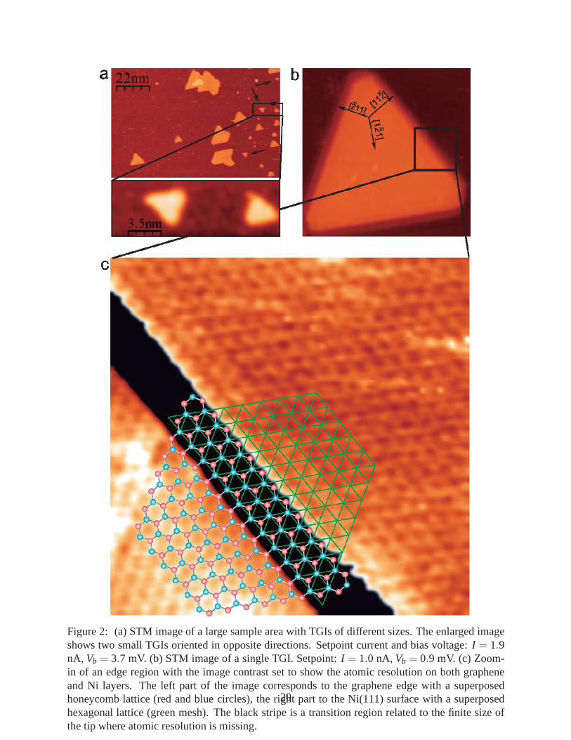
Figure 2: (a) STM image of a large sample area with TGIs of different sizes. The enlarged imageshows two small TGIs oriented in opposite directions. Setpoint current and bias voltage:I = 1.9nA, Vb = 3.7 mV. (b) STM image of a single TGI. Setpoint:I = 1.0 nA,Vb = 0.9 mV. (c) Zoom-in of an edge region with the image contrast set to show the atomic resolution on both grapheneand Ni layers. The left part of the image corresponds to the graphene edge with a superposedhoneycomb lattice (red and blue circles), the right part to the Ni(111) surface with a superposedhexagonal lattice (green mesh). The black stripe is a transition region related to the finite size ofthe tip where atomic resolution is missing.
20

Figure 3: Relaxed model configurations of TGIs on Ni(111) calculated by DFT, together with thecorresponding energies per C atom in meV. The latter are given with respect to E0, the energy ofthe most stable TGI.
21
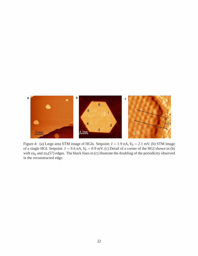
Figure 4: (a) Large area STM image of HGIs. Setpoint:I = 1.9 nA,Vb = 2.1 mV. (b) STM imageof a single HGI. Setpoint:I = 9.6 nA,Vb = 0.9 mV. (c) Detail of a corner of the HGI shown in (b)with zzh and zzt(57) edges. The black lines in (c) illustrate the doubling ofthe periodicity observedin the reconstructed edge.
22
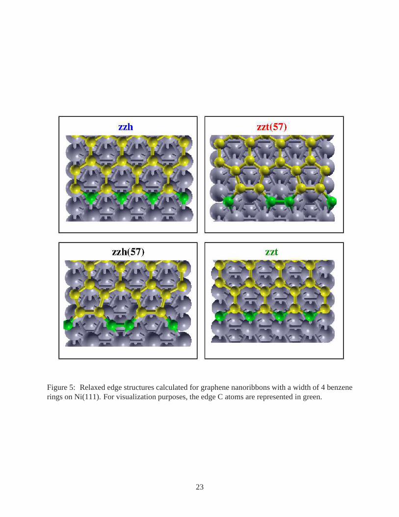
Figure 5: Relaxed edge structures calculated for graphene nanoribbons with a width of 4 benzenerings on Ni(111). For visualization purposes, the edge C atoms are represented in green.
23
Edge conformation0.2 0.2
0.3 0.3
0.4 0.4
0.5 0.5
0.6 0.6
0.7 0.7
Edg
e en
ergy
(eV
/Å)
zzt(57)zzh
zztzzh(57)
zzhzzh
ac ad
a)
b)
zz (57) t
Figure 6: (a) Formation energies of graphene zz edges on Ni(111). (b) Equilibrium shape ofgraphene nanoislands on Ni(111) obtained by minimizing theedge energy. If edge reconstructionis allowed the islands exhibit zzh and reconstructed zzt(57) edges, adopting an hexagon-like shape.If reconstruction is inhibited the islands have a triangle-like shape and exhibit zzh and reconstructedarmchair edges.
24