switching regulators (integrated fet) 3.3v and 5v output...
TRANSCRIPT

Datasheet
. 1/28
TSZ02201-0W1W0AL00030-1-2© 2013 ROHM Co., Ltd. All rights reserved. 07.Jul.2014 Rev.003TSZ22111・14・001
www.rohm.com
Product structure:Silicon monolithic integrated circuit This product is not designed protection against radioactive rays
Switching Regulators (Integrated FET)
3.3V and 5V output Low Iq DC/DC Converters BD99010EFV-M BD99011EFV-M
General Description
The BD99010EFV-M and BD99011EFV-M are ultra low Iq Step-down DC/DC converters with integrated power MOSFETs for 3.3V and 5V, respectively. The SLLMTM (Simple Light Load Mode) control ensures an ultra low quiescent current and high efficiency at low load situation as well as a high efficiency at high load situations while maintaining a regulated output voltage. The product is compliant with automotive standards and accommodates a maximum voltage of 42V. The minimum input voltage is 3.6 V in order to sustain output at cold cranking conditions. The current mode regulation loop gives a fast transient response and easy phase compensation. The BD99010EFV-M and BD99011EFV-M are available in a HTSSOP-B24 package. In an application it requires a small number of external components and small PCB footprint.
Features Low Quiescent Operating Current: 22μA Simple Light Load Mode (SLLM) Supports Cold Cranking Down to 3.6V Output Voltage Accuracy: ±2% Synchronous Rectifier Soft Start Chip Enable pin compatible with CMOS logic and
battery voltages Forced PMW Mode Function Current Mode Control with External Compensation
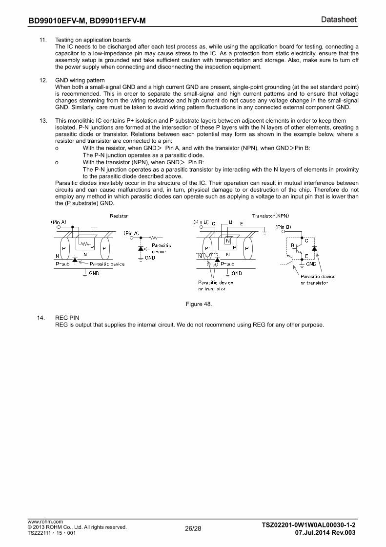
Circuit Over Current Protection, Short Circuit Protection,
Over Voltage Protection for VOUT, Under Voltage Lock Out for VIN and Thermal Protection Circuits
Key Specifications Input Voltage Range: 3.6V to 35V
(Absolute Maximum42V) (Initial startup is over 3.9V) Output Voltage Range: 3.3V (BD99010EFV-M)
5V (BD99011EFV-M) Switch Output Current: 2A(Max) Switching Frequency: 200kHz to 500kHz Pch FET ON Resistance: 170mΩ(Typ) Nch FET ON Resistance: 130mΩ(Typ) Operating Temperature Range: -40°C to +105°C AEC-Q100 Qualified
Package W(Typ) x D(Typ) x H(Max)
HTSSOP-B24 7.80mm x 7.600mm x 1.00mm
Applications Automotive Battery Powered Supplies(Cluster Panel,
Car Multimedia) Industrial/Consumer Supplies.
Typical Application Circuit
Figure1. Reference application circuit

DatasheetDatasheet
2/28 TSZ02201-0W1W0AL00030-1-2© 2013 ROHM Co., Ltd. All rights reserved.
07.Jul.2014 Rev.003
www.rohm.com
TSZ22111・15・001
BD99010EFV-M, BD99011EFV-M
Pin Configuration
<TOP VIEW>
Figure 2. Pin configuration Pin Description
Pin No. Pin Name Function Pin No. Pin Name Function
1 N.C. No connection 13 FPWM Forced PWM mode pin
2 PVIN Power input supply pin 14 N.C. No connection
3 PVIN Power input supply pin 15 EN Enable pin, active high
4 N.C. No connection 16 VOUT Output pin
5 VIN Input supply pin 17 REG_L Internal logic supply pin
6 N.C. No connection 18 N.C. No connection
7 VREGB FET driver drive power supply pin 19 SW Switching output pin
8 N.C. No connection 20 SW Switching output pin
9 RT Switching frequency setting pin 21 N.C. No connection
10 COMP Error amplifier output pin 22 PGND Power GND pin
11 GND GND pin 23 PGND Power GND pin
12 REG Internal regulator output pin 24 PGND Power GND pin
1
2
3
4
5
6
7
8
9
10
11
12
24
23
22
21
20
19
18
17
16
15
14
13
PVIN
PVIN
VIN
VREGB
RT
COMP
GND
REG
PGND
PGND
SW
VOUT
EN
PGND
SW
FPWM
N.C.
N.C.
N.C.
N.C.
N.C.
N.C.
N.C.
REG _ L
DatasheetDatasheet
3/28 TSZ02201-0W1W0AL00030-1-2© 2013 ROHM Co., Ltd. All rights reserved.
07.Jul.2014 Rev.003
www.rohm.com
TSZ22111・15・001
BD99010EFV-M, BD99011EFV-M
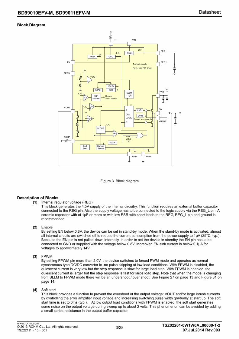
Block Diagram
EN
FPWM
VREF
RT VIN
OSC
REG
SCPcounter
IBIAS
UVLO
TSD
SLLMLogic
S
DRV
LOGIC
R
SLOPE
VOUT
COMP
SoftStart
CurrentSense
OCP
LVS
REG
REG_L
VREGB
SW
PVIN
4.5V
For logic supply
1.2V
1.2V
FPWM
0.8VReleaseafter 1024clk
1.2V
1.2V
SCP
OVP
ERR
PWM
OVPUVLOTSD
GND PGND
LVIN
Detect Vin under 6V
For L-side FET driver
Figure 3. Block diagram Description of Blocks
(1) Internal regulator voltage (REG) This block generates the 4.5V supply of the internal circuitry. This function requires an external buffer capacitor connected to the REG pin. Also the supply voltage has to be connected to the logic supply via the REG_L pin. A ceramic capacitor with of 1μF or more or with low ESR with short leads to the REG, REG_L pin and ground is recommended.
(2) Enable By setting EN below 0.8V, the device can be set in stand-by mode. When the stand-by mode is activated, almost all internal circuits are switched off to reduce the current consumption from the power supply to 1μA (25°C, typ.). Because the EN pin is not pulled-down internally, in order to set the device in standby the EN pin has to be connected to GND or supplied with the voltage below 0.8V. Moreover, EN sink current is below 0.1μA for voltages to approximately 14V.
(3) FPWM By setting FPWM pin more than 2.0V, the device switches to forced PWM mode and operates as normal synchronous type DC/DC converter ie. no pulse skipping at low load conditions. With FPWM is disabled, the quiescent current is very low but the step response is slow for large load step. With FPWM is enabled, the quiescent current is larger but the step response is fast for large load step. Note that when the mode is changing from SLLM to FPWM mode there will be an undershoot / over shoot. See Figure 27 on page 13 and Figure 31 on page 14.
(4) Soft start This block provides a function to prevent the overshoot of the output voltage: VOUT and/or large inrush currents by controlling the error amplifier input voltage and increasing switching pulse width gradually at start up. The soft start time is set to 6ms (typ.). At low output load conditions with FPWM is enabled, the soft start generates some noise on the output voltage during sweep up to about 2 volts. This phenomenon can be avoided by adding a small series resistance in the output buffer capacitor.

DatasheetDatasheet
4/28 TSZ02201-0W1W0AL00030-1-2© 2013 ROHM Co., Ltd. All rights reserved.
07.Jul.2014 Rev.003
www.rohm.com
TSZ22111・15・001
BD99010EFV-M, BD99011EFV-M
(5) Error amplifier The error amplifier compares the output feedback voltage to the 1.2V internal reference voltage and outputs the difference as current to the COMP pin, which voltage is used to determine the switching duty cycle. A t initial startup when the soft start works, the COMP voltage is limited to the soft start voltage. Moreover, the external resistor and capacitor are required to COMP pin as phase compensation circuit.
(6) PWM modulator. The PWM modulator converts the voltage at the COMP terminal to a continuous variable duty cycle that controls the output power transistors. At very low input voltages the duty cycle can become 1 indicating the high-side power transistor continuously in on-state. At very high input voltages the duty cycle becomes very small but limited at an on-time of about 200ns. It should be noted that at high oscillation frequency settings this could lead to random pulse skipping. For instance at 500 kHz the duty cycle is limited to values larger than 200ns / 2µs = 10%. This means that for 3.3V output the input voltage is limited to 33 V when avoiding random pulse skips. In case, a higher input voltage is required the switching frequency has to be chosen lower.
(7) Oscillator The oscillation frequency is determined by the current going through the external resistor RT at constant voltage of ca. 0.3V. The frequency can be set in the range between 200kHz to 500kHz. It should be noted that the frequency increases ca. 10% when the input voltage VIN is lower than 4.5 V because in that condition the internal supply voltage VREG is also lowered.
(8) VREGB pin and Low input voltage detection (LVIN)
VREGB is the supply voltage of the high-side driver and output power transistor. VREGB voltage is referenced from PVIN at voltage with 7.2V (typ.). When VIN voltage becomes below 6V (typ.), the LVIN circuit is activated and VREGB is shorted to GND. By doing so the output power transistor is driven with the full supply voltage at cold cranking conditions. An external capacitor is required between PVIN and VREGB pin. A ceramic capacitor with 0.1μF or low ESR type is recommended.
(9) Overcurrent protection (OCP) The overcurrent protection is activated when the SW current exceeds 3.3A (typ.). Once activated the ON duty cycle will be limited and the output voltage lowered.
(10) Short circuit protection (SCP) and SCP counter The short circuit protection is activated after the output voltage (FB voltage) drops below 67% of the nominal voltage level and the overcurrent protection is activated (except during startup). This indicated an output short and the short circuit protection will be activated. When the short circuit protection is activated, for a period of 1024 cycles of oscillation frequency, switching will be terminated by turning off the output transistors and the SS and COMP pins discharged. After this time out period the switching will resume including soft start.
(11) Under voltage lockout circuit (UVLO) If the VIN drops below 3.4V (typ.) the UVLO is activated and the BD99010 and BD99011 is turned off.
(12) Thermal shutdown (TSD) If the chip temperature (Tj) reaches or exceeds ca. 175°C (typ.) the output is turned off. Switching will resume with soft start when the temperature drops below ca. 150 °C (typ.)
(13) Over voltage protection(OVP)
The BD9901x is equipped with an integrated over voltage protection (OVP) for output voltages exceeding 10% above nominal output voltage. The OVP terminates switching until the output voltage drops below nominal value again before resuming normal operation. The OVP is intended as a last-resort protection mechanism and should never trigger in well-designed applications. Essentially there are two main root causes for an OVP event in a practical application: Extremely fast and extreme input voltage variations, for instance a supply voltage step from a few volts to a
maximum of 36V in a few micro seconds. Normally, an appropriate input filter should prevent this from occurring.
Extreme load current variations from maximum current to zero in very short time, for instance caused by a mechanical fuse or relay to trip.
Also it should be noted that when the output load is zero for a longer time while the ambient temperature is extremely high (above 105ºC) a small leakage current through the high-side switch inside the BD9901x can cause the output voltage to be higher than the OVP level. In case this might happen in the application under extraordinary conditions, it is advised to bleed a small output current exceeding this leakage. Naturally, this current increases the ultra-low quiescent current of 22 µA of a typical BD9901x application.

DatasheetDatasheet
5/28 TSZ02201-0W1W0AL00030-1-2© 2013 ROHM Co., Ltd. All rights reserved.
07.Jul.2014 Rev.003
www.rohm.com
TSZ22111・15・001
BD99010EFV-M, BD99011EFV-M
Operation The BD99010EFV-M and BD99011EFV-M are a synchronous rectifying step-down switching regulator with fast transient response by the current mode PWM control system. These operate as PWM (Pulse Width Modulation) mode for heavy load, and it operates as SLLM (Simple Light Load Mode) operation for the light load to improve efficiency. When FPWM is enabled, the SLLM is disabled and these devices operate only the current mode PWM control. (1) Synchronous rectifier The application does not require an external Schottky diode as commonly used in conventional DC/DC converter IC’s. The low-side power transistor provides two advantages: it reduces the switching losses by careful on-chip timing to prevent shoot-through and improves the leakage current (resulting in large quiescent current) at high operating temperatures. (2) Current mode PWM control Synthesizes an additional PWM control signal, representing the inductor current next to the conventional PWM control signal, representing the output voltage of the converter. The current feedback loop is essential to achieve regulation loop stability under all load conditions at so-called continuous condition Buck conversion. (a) PWM (Pulse Width Modulation) control
The PWM circuit operates as follows: At the start of every switch cycle the oscillator sets the flip-flop that controls the power transistors. This flip-flop is reset again when the slope signal (representing the inductor current) is exceeding the COMP signal (representing the difference between output voltage and internal reference).
(b) SLLM (Simple Light Load Mode) control
For small output currents, this device automatically switches to SLLM. In SLLM, the device operates in PWM control by comparing the output voltage with an internal reference voltage. When the output voltages drops below the reference voltage the output makes several switching pulses in order to raise the output voltage above reference level again. Next, switching pulses are skipped because the SW output is off. Depending on the output load, the controller now waits at very low current consumption until the output voltage is lower than the reference voltage to resume switching. When the time in between the switching pulse skip becomes short the device exits the SLLM mode and resumes normal continuous switching again. The load level of the switching pulse skip is changed by the input voltage and inductor value.
Figure 4. Diagram of current mode PWM control
Figure 5. PWM switching timing chart Figure 6. SLLM switching timing chart

DatasheetDatasheet
6/28 TSZ02201-0W1W0AL00030-1-2© 2013 ROHM Co., Ltd. All rights reserved.
07.Jul.2014 Rev.003
www.rohm.com
TSZ22111・15・001
BD99010EFV-M, BD99011EFV-M
Below the SW and VOUT waveforms during SLLM and PWM are shown.
Figure 7. SW and VOUT waveforms at SLLM Figure 8. SW and VOUT waveforms at PWM (Light load) (Heavy load)
Recommended specification for SLLM
The figure below shows the relation between the input / output currents and output ripple voltage at SLLM. SLLM at light load is different from regular PWM and has an increased output ripple voltage. During SLLM, the transient response for heavy loads is also slower. A recommendation is shown below on how to minimize the output ripple voltage and load changes at each of the control modes.
Figure 9. Ripple voltage and load response at SLLM
DatasheetDatasheet
7/28 TSZ02201-0W1W0AL00030-1-2© 2013 ROHM Co., Ltd. All rights reserved.
07.Jul.2014 Rev.003
www.rohm.com
TSZ22111・15・001
BD99010EFV-M, BD99011EFV-M
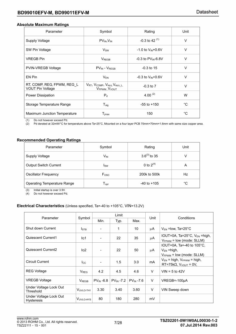
Absolute Maximum Ratings
Parameter Symbol Rating Unit
Supply Voltage PVIN,VIN -0.3 to 42 (1) V
SW Pin Voltage VSW -1.0 to VIN+0.6V V
VREGB Pin VREGB -0.3 to PVIN-6.8V V
PVIN-VREGB Voltage PVIN - VREGB -0.3 to 15 V
EN Pin VEN -0.3 to VIN+0.6V V
RT, COMP, REG, FPWM, REG_L VOUT Pin Voltage
VRT, VCOMP, VREG, VREG_L,
VFPWM , VVOUT -0.3 to 7 V
Power Dissipation Pd 4.00 (2) W
Storage Temperature Range Tstg -55 to +150 °C
Maximum Junction Temperature Tjmax 150 °C
(1) Do not however exceed Pd. (2) Pd derated at 32mW/°C for temperature above Ta=25°C, Mounted on a four layer PCB 70mm×70mm×1.6mm with same size copper area.
Recommended Operating Ratings
Parameter Symbol Rating Unit
Supply Voltage VIN 3.6(3) to 35 V
Output Switch Current ISW 0 to 2(4) A
Oscillator Frequency FOSC 200k to 500k Hz
Operating Temperature Range Topr -40 to +105 °C
(3) Initial startup is over 3.9V. (4) Do not however exceed Pd.
Electrical Characteristics (Unless specified, Ta=-40 to +105°C, VIN=13.2V)
Parameter Symbol Limit
Unit Conditions Min. Typ. Max.
Shut down Current ISTB - 1 10 A VEN =low, Ta=25°C
Quiescent Current1 IQ1 - 22 35 A IOUT=0A, Ta=25°C, VEN =high, VFPWM = low (mode: SLLM)
Quiescent Current2 IQ2 - 22 50 A IOUT=0A, Ta=-40 to 105°C, VEN =high, VFPWM = low (mode: SLLM)
Circuit Current ICC - 1.5 3.0 mA VEN = high, VFPWM = high, RT=75kΩ, VVOUT = 0V,
REG Voltage VREG 4.2 4.5 4.6 V VIN = 5 to 42V
VREGB Voltage VREGB PVIN -6.8 PVIN -7.2 PVIN -7.6 V VREGB=-100μA
Under Voltage Lock Out Threshold VUVLO-TH1 3.30 3.40 3.60 V VIN Sweep down
Under Voltage Lock Out Hysteresis VUVLO-HYS 80 180 280 mV

DatasheetDatasheet
8/28 TSZ02201-0W1W0AL00030-1-2© 2013 ROHM Co., Ltd. All rights reserved.
07.Jul.2014 Rev.003
www.rohm.com
TSZ22111・15・001
BD99010EFV-M, BD99011EFV-M
Electrical Characteristics (Unless specified, Ta=-40 to +105°C, VIN=13.2V)
Output Voltage
BD99010 VOUT,3.3V
3.23 3.30 3.37 V VIN = 6.5 to 18V, PWM mode
3.17 (5) 3.30 (5) 3.43 (5) V VIN = 6.5 to 18V, SLLM Including output ripple (6)
3.1 3.30 - V VIN = 3.6V, ILoad = 0 to 1A Ta=25°C
BD99011 VOUT,5V
4.90 5.00 5.10 V VIN = 6.5 to 18V, PWM mode
4.80 (5) 5.00 (5) 5.20 (5) V VIN = 6.5 to 18V, SLLM Including output ripple (6)
4.5 4.73 - V VIN = 5V, ILoad = 0 to 1A Ta=25°C
High Side FET ON resistanceRONH - 170 340 mΩ
ISW =-50mA, VIN=13.2V Ta=25°C
RONH_LV - 265 500 mΩ ISW =-50mA, VIN=3.6V Ta=25°C
Low Side FET ON resistance RONL - 130 260 mΩ ISW =50mA, VIN=13.2V Ta=25°C
SW Leakage Current IOLEAK - - 10 A VIN = 42V, VSW = 0V, VEN =low, Ta=25°C
DC Output Current Limit IOLIMIT 2.4 (5) 3.3 (5) 4.2 (5) A
Oscillator Frequency FOSC 320 400 480 kHz RT=75kΩ, VIN= 6.5 to 18V
Soft Start Time TSS 3 6 11 ms
Enable
EN Threshold VIH-EN 2.0 - - V
VIL-EN - - 0.8 V
EN Hysteresis VEN-HYS 50 100 200 mV
EN Sink Current IEN - 0.1 1.0 A VEN =5V, Ta=25°C
Forced PWM mode
FPWM Threshold VIH-PWM 2.0 - - V PWM mode
VIL-PWM - - 0.8 V
FPWM Hysteresis VFPWM-HYS 200 330 460 mV
FPWM Sink Current IFPWM 4.0 7.5 12.0 A VFPWM =5V
(5) Not production tested. Guaranteed by design. (6) Using external components on page 17 and 18.

DatasheetDatasheet
9/28 TSZ02201-0W1W0AL00030-1-2© 2013 ROHM Co., Ltd. All rights reserved.
07.Jul.2014 Rev.003
www.rohm.com
TSZ22111・15・001
BD99010EFV-M, BD99011EFV-M
Typical Performance Curves
Figure 10. Efficiency Log Scale (BD99010EFV-M : VOUT.3.3V)
Figure 11. Efficiency Linear Scale (BD99010EFV-M : VOUT.3.3V)
Figure 12. Efficiency Log Scale (BD99011EFV-M : VOUT.5V)
Figure 13. Efficiency Linear Scale (BD99011EFV-M: VOUT.5V)
SLLM
PWM
0
10
20
30
40
50
60
70
80
90
100
0.01 0.1 1 10 100 1000 10000
Effi
cie
ncy
[%
]
ILOAD Log scale [mA]
VIN=13.2Vf=400kHz
PWM
SLLM
60
65
70
75
80
85
90
95
100
0 500 1000 1500 2000
Effi
cie
ncy
[%]
ILOAD Linear scale [mA]
VIN=13.2Vf=400kHz
SLLM
PWM
0
10
20
30
40
50
60
70
80
90
100
0.01 0.1 1 10 100 1000 10000
Effi
cie
ncy
[%
]
ILOAD Log scale [mA]
VIN=13.2Vf=400kHz
PWM
SLLM
60
65
70
75
80
85
90
95
100
0 500 1000 1500 2000
Effi
cie
ncy
[%]
ILOAD Linear scale [mA]
VIN=13.2Vf=400kHz

DatasheetDatasheet
10/28 TSZ02201-0W1W0AL00030-1-2© 2013 ROHM Co., Ltd. All rights reserved.
07.Jul.2014 Rev.003
www.rohm.com
TSZ22111・15・001
BD99010EFV-M, BD99011EFV-M
0
5
10
15
20
25
30
35
40
45
50
0 5 10 15 20 25 30 35 40
I IN[µ
A]
Input Voltage [V]
0
5
10
15
20
25
30
35
40
45
50
-40 -20 0 20 40 60 80 100I IN
[uA
]Temperature[°C]
Figure 14. IIN vs. Input Voltage at No Load Figure 15. IIN vs. Temperature at No Load
Figure 16. IIN vs. ILOAD Figure 17. Frequency vs. Temperature
BD99011EFV-M
BD99010EFV-M
VIN=13.2VIOUT=0A
Ta=25°C IOUT=0A
320
340
360
380
400
420
440
460
480
-40 -20 0 20 40 60 80 100
Fre
qu
en
cy [k
Hz]
Temperature [°C]
0
50
100
150
200
250
300
350
400
10 100 1000
I IN [u
A]
ILOAD Log Scale [uA]
Ta=25°C VIN=13.2V
BD99011EFV-M
BD99010EFV-M

DatasheetDatasheet
11/28 TSZ02201-0W1W0AL00030-1-2© 2013 ROHM Co., Ltd. All rights reserved.
07.Jul.2014 Rev.003
www.rohm.com
TSZ22111・15・001
BD99010EFV-M, BD99011EFV-M
3.23
3.24
3.25
3.26
3.27
3.28
3.29
3.30
3.31
3.32
3.33
3.34
3.35
3.36
3.37
0 500 1000 1500 2000
Ou
tpu
t Vo
ltag
e [V
]
ILOAD [mA]
Ta=25
Ta=-40
Ta=105
3.23
3.24
3.25
3.26
3.27
3.28
3.29
3.30
3.31
3.32
3.33
3.34
3.35
3.36
3.37
5 10 15 20 25 30 35 40
Ou
tpu
t Vo
ltag
e [V
]
Input Voltage [V]
Ta=25°C
Ta=-40°C
Ta=105°C
3.23
3.24
3.25
3.26
3.27
3.28
3.29
3.30
3.31
3.32
3.33
3.34
3.35
3.36
3.37
5 10 15 20 25 30 35 40
Ou
tpu
t Vo
ltag
e [V
]
Input Voltage[V]
Ta=25°C
Ta=-40°C
Ta=105°C
Figure 18. Line Regulation 1 (BD99010EFV-M: VOUT.3.3V)
Figure 19. Line Regulation 2 (BD99010EFV-M: VOUT.3.3V)
Figure 20. Load Regulation (BD99010EFV-M: VOUT.3.3V)
Figure 21. Output Voltage vs. Temperature (BD99010EFV-M: VOUT.3.3V)
f=400kHz ILOAD=1A VFPWM=low
f=400kHzILOAD=100µA VFPWM=low
VIN=13.2V f=400kHz VFPWM=low
3.23
3.24
3.25
3.26
3.27
3.28
3.29
3.30
3.31
3.32
3.33
3.34
3.35
3.36
3.37
-40 -20 0 20 40 60 80 100
Out
pu
t Vo
ltag
e [V
]
Temperature[°C]

DatasheetDatasheet
12/28 TSZ02201-0W1W0AL00030-1-2© 2013 ROHM Co., Ltd. All rights reserved.
07.Jul.2014 Rev.003
www.rohm.com
TSZ22111・15・001
BD99010EFV-M, BD99011EFV-M
4.90
4.92
4.94
4.96
4.98
5.00
5.02
5.04
5.06
5.08
5.10
5 10 15 20 25 30 35 40
Ou
tpu
t Vo
ltag
e [V
]
Input Voltage[V]
Ta=25°C
Ta=-40°C
Ta=105°C
4.90
4.92
4.94
4.96
4.98
5.00
5.02
5.04
5.06
5.08
5.10
5 10 15 20 25 30 35 40O
utp
ut V
olta
ge
[V]
Input Voltage [V]
Ta=25°C
Ta=-40°C
Ta=105°C
4.90
4.92
4.94
4.96
4.98
5.00
5.02
5.04
5.06
5.08
5.10
0 500 1000 1500 2000
Ou
tpu
t Vo
ltag
e [V
]
ILOAD [mA]
Ta=25
Ta=-40
Ta=1054.90
4.92
4.94
4.96
4.98
5.00
5.02
5.04
5.06
5.08
5.10
-40 -20 0 20 40 60 80 100
Ou
tpu
t Vo
ltag
e [V
]
Temperature[°C]
Figure 22. Line Regulation 1 (BD99011EFV-M: VOUT.5V)
Figure 23. Line Regulation 2 (BD99011EFV-M: VOUT.5V)
Figure 24. Load Regulation (BD99011EFV-M: VOUT.5V)
Figure 25. Output Voltage vs. Temperature (BD99011EFV-M: VOUT.5V)
f=400kHz ILOAD=1A VFPWM=low
f=400kHzILOAD=100µA VFPWM=low
VIN=13.2V f=400kHz VFPWM=low

DatasheetDatasheet
13/28 TSZ02201-0W1W0AL00030-1-2© 2013 ROHM Co., Ltd. All rights reserved.
07.Jul.2014 Rev.003
www.rohm.com
TSZ22111・15・001
BD99010EFV-M, BD99011EFV-M
Figure 26. Transient Response (BD99010EFV-M: VOUT.3.3V)
Figure 27. Mode Transition (SLLM ⇔ FWPM) (BD99010EFV=M: VOUT.3.3V)
Figure 28. Slow Input Ramp Up and Down (BD99010EFV-M: VOUT.3.3V)
Figure 29. VIN Cranking (BD99010EFV-M: VOUT.3.3V)
SW 5V/div
VIN 5V/div
VOUT2V/div
ILOAD 2A/div
VOUT (AC coupled) 100mV/div
FPWM 5V/div
SW 10V/div
VIN 5V/div
SW 5V/div
VOUT2V/div
VOUT (AC coupled) 100mV/div
ILOAD 1A/div
VIN=13.2V, f=400kHz
200mA
2A

DatasheetDatasheet
14/28 TSZ02201-0W1W0AL00030-1-2© 2013 ROHM Co., Ltd. All rights reserved.
07.Jul.2014 Rev.003
www.rohm.com
TSZ22111・15・001
BD99010EFV-M, BD99011EFV-M
Figure 30. Transient Response (BD99011EFV-M: VOUT.5V)
Figure 31. Mode Transition (SLLM ⇔ FWPM) (BD99011EFV-M: VOUT.5V)
Figure 32. Slow Input Ramp Up and Down (BD99011EFV-M: VOUT.5V)
Figure 33. VIN Cranking (BD99011EFV-M: VOUT.5V)
SW 5V/div
VIN 5V/div
VOUT5V/div
ILOAD 2A/div
VOUT (AC coupled) 100mV/div
FPWM 5V/div
SW 10V/div
VIN 5V/div
SW 5V/div
VOUT5V/div
VIN=3.6V
VOUT (AC coupled) 100mV/div
ILOAD 1A/div
VIN=13.2V, f=400kHz
200mA
2A

DatasheetDatasheet
15/28 TSZ02201-0W1W0AL00030-1-2© 2013 ROHM Co., Ltd. All rights reserved.
07.Jul.2014 Rev.003
www.rohm.com
TSZ22111・15・001
BD99010EFV-M, BD99011EFV-M
Figure 34. EN Sink Current Figure 35. FPWM Sink Current
Figure 36. Measurement Figure
0
2
4
6
8
10
12
14
16
18
5 10 15 20 25 30 35 40
EN
Sin
k C
urr
en
t [μ
A]
EN Voltage [V]
Ta=25°C
Ta=-40°C
Ta=105°C
0
2
4
6
8
10
12
14
1.0 1.5 2.0 2.5 3.0 3.5 4.0 4.5 5.0 5.5 6.0 6.5 7.0F
PW
M S
ink
Cu
rre
nt
[μA
]FPWM Voltage [V]
Ta=25°C
Ta=-40°C
Ta=105°C
PVIN
PVIN
VIN
COMP
GND
RT
VREGB
REG
C6
C1
RRT R1
C7 C5
EN
REG_L
FPWM
SW
SW
VOUT
C8
COUT3 COUT4 COUT5
L1
R100
EN
FPWM
C2CIN
VIN
GND PGND
VOUT
(1)
PGND
PGND
PGND
PGNDPGNDPGND
GND GND GND GND
GND PGNDPGNDPGND
ILOAD
IIN
Input Voltage

DatasheetDatasheet
16/28 TSZ02201-0W1W0AL00030-1-2© 2013 ROHM Co., Ltd. All rights reserved.
07.Jul.2014 Rev.003
www.rohm.com
TSZ22111・15・001
BD99010EFV-M, BD99011EFV-M
Timing Chart (1) Startup operations
Figure 37. Timing Chart 1 (Start up operation)
(2) Protection operations (VIN,PVIN=13.2V, VEN=high)
Figure 38. Timing Chart 2 (Protection operation)
VIN, PVIN
Internal
soft start
REG
EN
UVLO release(typ : 3.58V)
COMP
SW
VOUT

DatasheetDatasheet
17/28 TSZ02201-0W1W0AL00030-1-2© 2013 ROHM Co., Ltd. All rights reserved.
07.Jul.2014 Rev.003
www.rohm.com
TSZ22111・15・001
BD99010EFV-M, BD99011EFV-M
Applications
Figure 39. Application circuit
BD99010EFV-M
No Component
Name Component
Value Description Product Name Comment
1 CIN(1) 220µF Capacitor, 50V, electrolytic -
2 C1 4.7µF Capacitor, 50V, ceramic GCM32ER71H475KA55
3 C2 - Capacitor, 50V, ceramic -
4 COUT3 22µF Capacitor, 10V, ceramic GCM32ER71A226KE12
5 COUT4 22µF Capacitor, 10V, ceramic GCM32ER71A226KE12
6 COUT5 22µF Capacitor, 10V, ceramic GCM32ER71A226KE12
7 C5 1µF Capacitor, 16V, ceramic GCM188R71C105KA64
8 C6 0.1µF Capacitor, 50V, ceramic GCM188R71H104KA57
9
C7
2200pF Capacitor, 50V, ceramic GCM188R71H222KA37 f=200kHz
1500pF Capacitor, 50V, ceramic GCM188R71H152KA37 f=300kHz
1000pF Capacitor, 50V, ceramic GCM188R71H102KA37 f=400kHz
1000pF Capacitor, 50V, ceramic GCM188R71H102KA37 f=500kHz
10 C8 - Capacitor, 16V, ceramic -
11
R1
27kΩ Resistor, MCR03EZP Series f=200kHz
27kΩ Resistor, MCR03EZP Series f=300kHz
33kΩ Resistor, MCR03EZP Series f=400kHz
33kΩ Resistor, MCR03EZP Series f=500kHz
12
RRT
164kΩ Resistor, MCR03EZP Series f=200kHz
104kΩ Resistor, MCR03EZP Series f=300kHz
75kΩ Resistor, MCR03EZP Series f=400kHz
58kΩ Resistor, MCR03EZP Series f=500kHz
13 R100 0Ω Resistor, MCR03EZP Series
14 L1
22µH Inductor CLF10040T-220M-H f=200kHz
15µH Inductor CLF10040T-150M-H f=300kHz
10µH Inductor CLF10040T-100M-H f=400kHz
10µH Inductor CLF10040T-100M-H f=500kHz (1): Refer to Setting the input capacitor in page 20/28.
(1): Refer to Setting the input capacitor in page 20/28.
DatasheetDatasheet
18/28 TSZ02201-0W1W0AL00030-1-2© 2013 ROHM Co., Ltd. All rights reserved.
07.Jul.2014 Rev.003
www.rohm.com
TSZ22111・15・001
BD99010EFV-M, BD99011EFV-M
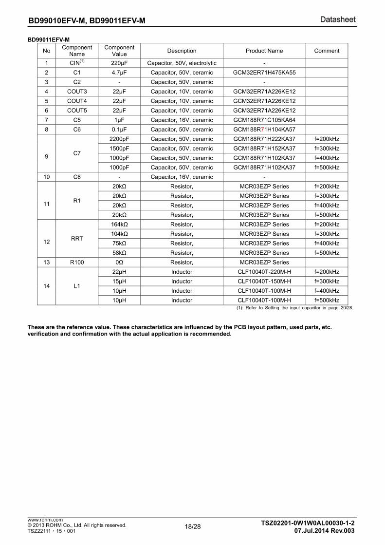
BD99011EFV-M
No Component
Name Component
Value Description Product Name Comment
1 CIN(1) 220µF Capacitor, 50V, electrolytic -
2 C1 4.7µF Capacitor, 50V, ceramic GCM32ER71H475KA55
3 C2 - Capacitor, 50V, ceramic -
4 COUT3 22µF Capacitor, 10V, ceramic GCM32ER71A226KE12
5 COUT4 22µF Capacitor, 10V, ceramic GCM32ER71A226KE12
6 COUT5 22µF Capacitor, 10V, ceramic GCM32ER71A226KE12
7 C5 1µF Capacitor, 16V, ceramic GCM188R71C105KA64
8 C6 0.1µF Capacitor, 50V, ceramic GCM188R71H104KA57
9
C7
2200pF Capacitor, 50V, ceramic GCM188R71H222KA37 f=200kHz
1500pF Capacitor, 50V, ceramic GCM188R71H152KA37 f=300kHz
1000pF Capacitor, 50V, ceramic GCM188R71H102KA37 f=400kHz
1000pF Capacitor, 50V, ceramic GCM188R71H102KA37 f=500kHz
10 C8 - Capacitor, 16V, ceramic -
11
R1
20kΩ Resistor, MCR03EZP Series f=200kHz
20kΩ Resistor, MCR03EZP Series f=300kHz
20kΩ Resistor, MCR03EZP Series f=400kHz
20kΩ Resistor, MCR03EZP Series f=500kHz
12
RRT
164kΩ Resistor, MCR03EZP Series f=200kHz
104kΩ Resistor, MCR03EZP Series f=300kHz
75kΩ Resistor, MCR03EZP Series f=400kHz
58kΩ Resistor, MCR03EZP Series f=500kHz
13 R100 0Ω Resistor, MCR03EZP Series
14 L1
22µH Inductor CLF10040T-220M-H f=200kHz
15µH Inductor CLF10040T-150M-H f=300kHz
10µH Inductor CLF10040T-100M-H f=400kHz
10µH Inductor CLF10040T-100M-H f=500kHz (1): Refer to Setting the input capacitor in page 20/28.
These are the reference value. These characteristics are influenced by the PCB layout pattern, used parts, etc. verification and confirmation with the actual application is recommended.
DatasheetDatasheet
19/28 TSZ02201-0W1W0AL00030-1-2© 2013 ROHM Co., Ltd. All rights reserved.
07.Jul.2014 Rev.003
www.rohm.com
TSZ22111・15・001
BD99010EFV-M, BD99011EFV-M
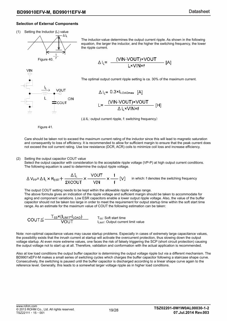
Selection of External Components (1) Setting the Inductor (L) value
The inductor-value determines the output current ripple. As shown in the following equation, the larger the inductor, and the higher the switching frequency, the lower the ripple current.
Figure 40. The optimal output current ripple setting is ca. 30% of the maximum current.
(ΔIL: output current ripple, f: switching frequency)
Figure 41.
Care should be taken not to exceed the maximum current rating of the inductor since this will lead to magnetic saturation and consequently to loss of efficiency. It is recommended to allow for sufficient margin to ensure that the peak current does not exceed the coil current rating. Use low resistance (DCR, ACR) coils to minimize coil loss and increase efficiency.
(2) Setting the output capacitor COUT value
Select the output capacitor with consideration to the acceptable ripple voltage (VP-P) at high output current conditions. The following equation is used to determine the output ripple voltage.
in which: f denotes the switching frequency
The output COUT setting needs to be kept within the allowable ripple voltage range. The above formula gives an indication of the ripple voltage and sufficient margin should be taken to accommodate for aging and component variations. Low ESR capacitors enable a lower output ripple voltage. Also, the value of the buffer capacitor should not be taken too large in order to meet the requirement for output startup time within the soft start time range. As an estimate for the maximum value of COUT the following estimation can be taken:
TSS: Soft start time ILIMIT: Output current limit value Note: non-optimal capacitance values may cause startup problems. Especially in cases of extremely large capacitance values, the possibility exists that the inrush current at startup will activate the overcurrent protection, thus slowing down the output voltage startup. At even more extreme values, one faces the risk of falsely triggering the SCP (short circuit protection) causing the output voltage not to start up at all. Therefore, validation and conformation with the actual application is recommended. Also at low load conditions the output buffer capacitor is determining the output voltage ripple but via a different mechanism. The BD9901xEFV-M makes a small series of switching cycles which charges the buffer capacitor following a staircase shape curve. Consecutively, the switching is paused until the buffer capacitor is discharged according to a linear shape curve again to the reference level. Generally, this leads to a somewhat larger voltage ripple as in higher load conditions.

DatasheetDatasheet
20/28 TSZ02201-0W1W0AL00030-1-2© 2013 ROHM Co., Ltd. All rights reserved.
07.Jul.2014 Rev.003
www.rohm.com
TSZ22111・15・001
BD99010EFV-M, BD99011EFV-M
(3) Setting input capacitor
The input capacitor acts as (i) Decoupling capacitor (ii) Bulk capacitor. Decoupling capacitor: Ceramic capacitor of value 4.7μF to 10μF is necessary. The voltage rating should be > 1.2x max input voltage or > 2 x normal input voltage. It is better to place it as close as possible to PVIN pin and PGND pin. Bulk capacitor: It acts as a backup power supply and tries to keep the input potential when the input power supply drops. The low ESR electrolytic capacitor with large capacity is suitable for the bulk capacitor. Based on application appropriate value can be taken. When the impedance on the input side is high (long wiring from the power supply to VIN, etc.), the high capacity is needed In application, it is necessary to verify that there is no problem at output due to the decrease of VIN at transient response. Please be careful not to exceed the rated ripple current of the capacitor. The IRMS value of the input ripple current can be calculated with the expression below.
Figure 42.
In addition, in the automotive and other applications requiring high reliability, it is recommended that the multiple electrolytic capacitors are connected in parallel to avoid a dry up. In order to reduce a risk of destruction because of short in a ceramic capacitor, we recommend using 2 serials +2 parallel structure. Since the lineup also of what packed 2 series and 2 parallel structure in 1package, respectively is carried out by each capacitor supplier, please confirm to each supplier.
(4) Setting the switching frequency
The switching frequency is set with the resistor RT. The setting range is 200kHz to 500kHz.The relation between the resistance value and the oscillation frequency is shown in the table below. Selecting a resistor outside the range shown below may cause malfunctions of the switching regulator.
RT resistance Oscillation frequency
164 kΩ
128 kΩ
104 kΩ
88 kΩ
75 kΩ
66 kΩ
58 kΩ
200kHz
250kHz
300kHz
350kHz
400kHz
450kHz
500kHz

DatasheetDatasheet
21/28 TSZ02201-0W1W0AL00030-1-2© 2013 ROHM Co., Ltd. All rights reserved.
07.Jul.2014 Rev.003
www.rohm.com
TSZ22111・15・001
BD99010EFV-M, BD99011EFV-M
(5) Setting the phase compensation circuit
The phase compensation circuitry provides regulation loop stability and ensures sufficient regulation bandwidth for rapid load and supply voltage step responses. There are two conditions to avoid (near) negative feedback that causes regulation in stability:
(a) At the frequency of unity loop gain(0dB), fc. the phase delay should be 150° or less. (i.e. the so-called phase margin is 30° or higher)
(b) As the DC/DC converter application is sampled according to the switching frequency, fc should be set to 1/10 or less of the switching frequency.
In order to achieve sufficient rapid step response fc should be as high as possible and consequently the switching frequency has to be set as high as possible. The phase compensation is set by the capacitors and resistors serially connected to the COMP pin. Achieving stability by using the phase compensation is done by cancelling the 2 poles (error amp pole denoted as fp1 and power stage pole denoted as fp2) of the regulation loop by means of a zero, denoted as fz1, of the capacitor C3 in the phase compensation circuit. fp1, fp2 and fz1 are determined by the formulas below.
In the formula above, gm is the error amp Trans conductance (140 μA/V) and AV is the error amp voltage gain (2500 V/V)
Figure 43.
During startup in forced PWM mode at light loads the duty cycle of the regulator has to be very small and the regulation loop has a tendency to become marginally instable causing a large voltage ripple or noise. This noise during startup can be prevented by creating another zero, fz2, in the regulation loop with resistor ROUT. Please note that adding this resistor is effectively increasing the ESR of the output buffer capacitor and hence increasing
the ripple voltage according eq. 2. In practice a small value suffices to remove all noise during soft start while keeping a small ripple voltage of ca. 50mVP-P at high load situations. In case, the noise at low voltages during startup is not negatively affecting other system components the resistor ROUT can be omitted. Moreover, in case of the start-up at SLLM with light load, the ripple voltage does not become large during the soft start. This setting is obtained by using a simplified calculation, therefore, small adjustments in values in the actual application
may be required. Also as these characteristics are influenced by the substrate layout, load conditions, etc. validation and confirmation with the actual application at time of mass production design is recommended.
fz1=2π×C3×R1
1
fp1=2π×C3×AV
gm

DatasheetDatasheet
22/28 TSZ02201-0W1W0AL00030-1-2© 2013 ROHM Co., Ltd. All rights reserved.
07.Jul.2014 Rev.003
www.rohm.com
TSZ22111・15・001
BD99010EFV-M, BD99011EFV-M
PCB Layout Pattern The PCB layout greatly influences the stable operation of the IC. Depending on the PCB layout IC might not show its
original characteristics or might not function properly. Please note the following points when creation the PCB layout. Moreover, Fig 35 shows the recommended layout pattern
and component placement. The input capacitors C1, C2 and CIN should be placed as close as possible to the VIN, PVIN GND and PGND.
Especially, C1 and C2 should be placed as close as possible to PVIN and PGND pin. The output voltage feedback line VOUT should be separated from lines with a lot of noise such as the SW line.
The output capacitors COUT3, COUT4 and COUT5 should be placed in close proximity to inductor L1. The inductor L1 should be placed as close as close as possible to the SW pin. The pattern area of the SW node
should be as small as possible. EN pin has to be connected GND or supplied with the voltage below 0.8V to set the device in shut down mode
because the EN pin is not pulled-down internally. The exposed die pad on the bottom of the package has to be soldered to GND. Then the device is connected to GND
electrically and gets good thermal performance. The feedback frequency characteristics (phase margin) can be measured by inserting a resistor at the location of
R100 and using FRA. However, this should be shorted during normal operation. <TOP VIEW> <BOTTOM VIEW>
Figure 44. Reference layout pattern
VIN
VOUT
FPWM
PGND
GND
PGND
EN

DatasheetDatasheet
23/28 TSZ02201-0W1W0AL00030-1-2© 2013 ROHM Co., Ltd. All rights reserved.
07.Jul.2014 Rev.003
www.rohm.com
TSZ22111・15・001
BD99010EFV-M, BD99011EFV-M
0.0
0.5
1.0
1.5
2.0
2.5
3.0
3.5
4.0
4.5
0 20 40 60 80 100 120 140
PO
WE
R D
ISS
IPA
TIO
N:
Pd
[W
]
AMBIENT TEMPERATURE: Ta []
(1) 4.0W
(2) 2.8W
(3) 1.1W
Heat Dissipation The allowance maximum junction temperature Tj of BD99010EFV-M and BD99011EFV-M is 150. When the junction temperature becomes 150 or more, the thermal shutdown circuit operates, and the device becomes shut down. Therefore, it is necessary to design the system requirements and the board layout so that the junction temperature should not exceed 150 in the power-supply voltage, the output load, and the operating temperature rating. The maximum junction temperature can be determined from ambient temperature Ta, thermal resistance θja of package and heat dissipation P of IC by the following equation. Tj = Ta + θja × P [] Thermal resistance θja of the package changes depending on the number of layers and the area of the copper foil of the board etc. Heat dissipation PTOTAL of IC can be calculated by the next expression. PTOTAL = PICC + PRON + PSW [W] PICC = VIN × ICC ・・・ Heat dissipation in control circuit PRON = Ron × IOUT2 ・・・ Heat dissipation in output FET Ron = D × RONH + (1 - D) × RONL PSW = Tr × IOUT × VIN × Fosc ・・・ Heat dissipation in switching ICC : Circuit current (refer to page. 6) RONH : ON resistance of H-side FET (refer to page. 7) RONL : ON resistance of L-side FET (refer to page. 7) Fosc : Oscillator frequency D : ON duty (=VOUT/ VIN) IOUT : Output load current Tr : switching rise and fall time (approximately 20ns)
Power dissipation vs. temperature characteristics
(1) :Standalone IC
(2) :Mounted on a ROHM 2 layer standard board
(70mm×70mm×1.6mm glass-epoxy board)
(3) : Mounted on a ROHM 4 layer standard board
(70mm×70mm×1.6mm glass-epoxy board)
Figure 45. Power dissipation vs. temperature characteristics

DatasheetDatasheet
24/28 TSZ02201-0W1W0AL00030-1-2© 2013 ROHM Co., Ltd. All rights reserved.
07.Jul.2014 Rev.003
www.rohm.com
TSZ22111・15・001
BD99010EFV-M, BD99011EFV-M
I/O Equivalence Circuits
Figure 46. Equivalent circuit figure
SW, VREGB REG, REG_L VOUT
RT COMP
ENFPWM
※()is for BD99011EFV-M

DatasheetDatasheet
25/28 TSZ02201-0W1W0AL00030-1-2© 2013 ROHM Co., Ltd. All rights reserved.
07.Jul.2014 Rev.003
www.rohm.com
TSZ22111・15・001
BD99010EFV-M, BD99011EFV-M
Operational Notes 1. Absolute maximum ratings
Exceeding the absolute maximum rating for supply voltage, operating temperature or other parameters can result in damages to or destruction of the chip. In this event it also becomes impossible to determine the cause of the damage (e.g. short circuit, open circuit, etc). Therefore, if any special mode is being considered with values expected to exceed the absolute maximum ratings, implementing physical safety measures, such as adding fuses, should be considered.
2. GND electric potential
Keep the GND terminal potential at the lowest (minimum) potential under any operating condition. Furthermore, excluding the SW pin, the voltage of all pin should never drop below that of GND. In case there is a pin with a voltage lower than GND implement countermeasures such as using a bypass route.
3. Power dissipation
Should by any chance the power dissipation rating be exceeded the rise in temperature of the chip may result in deterioration of the properties of the chip. Therefore allow for sufficient margins to ensure use within the power dissipation rating.
4. Input power supply
Concerning the input pins VIN and PVIN, the layout pattern should be as short as possible and free from electrical interferences. In case the impedance of the input supply line is large, the resulting voltage drop at high load situation and low supply voltage will cause repeated UVLO cycles sometimes referred to as “chattering”. Therefore, the impedance of the input line should be so small that the worst case voltage drop is smaller than the UVLO hysteresis. To prevent damage to or destruction of the chip, the input filter which can be contain 0.5V/μs against the voltage of VIN and PNIN should be considered.
5. Electrical characteristics
The electrical characteristics given in this specification may be influenced by conditions such as temperature, supply voltage and external components. Transient characteristics should be sufficiently verified.
6. Thermal shutdown (TSD)
This IC incorporates and integrated thermal shutdown circuit to prevent heat damage to the IC. Normal operation should be within the power dissipation rating, if however the rating is exceeded for a continued period, the junction temperature (Tj) will rise and the TSD circuit will be activated and turn all output pins OFF. After the Tj falls below the TSD threshold the circuits are automatically restored to normal operation. Note that the TSD circuit operates in a situation that exceeds the absolute maximum ratings and therefore, under no circumstances, should the TSD circuit be used in a set design or for any purpose other than protecting the IC from heat damage.
7. Inter-pin shorting and mounting errors
Ensure that when mounting the IC on the PCB the direction and position are correct. Incorrect mounting may result in damaging the IC. Also, shorts caused by dust entering between the output, input and GND pin may result in damaging the IC.
8. In some applications, the VIN and pin potential might be reversed, possibly resulting in circuit internal damage or
damage to the elements. For example, while the external capacitor is charged, the VIN shorts to the GND. For the REG and REG_L output pin use a capacitor with a capacitance with less than 100μF. We also recommend using reverse polarity diodes in series or a bypass diode between all pins and the VBAT pin.
Figure 47. 9. Operation in strong electromagnetic fields
Use caution when operating in the presence of strong electromagnetic fields, as this may cause the IC to malfunction.
10. In applications where the output pin is connected to a large inductive load, a counter-EMF (electromotive force) might occur at startup or shutdown. A diode should be added for protection.
DatasheetDatasheet
26/28 TSZ02201-0W1W0AL00030-1-2© 2013 ROHM Co., Ltd. All rights reserved.
07.Jul.2014 Rev.003
www.rohm.com
TSZ22111・15・001
BD99010EFV-M, BD99011EFV-M
11. Testing on application boards The IC needs to be discharged after each test process as, while using the application board for testing, connecting a capacitor to a low-impedance pin may cause stress to the IC. As a protection from static electricity, ensure that the assembly setup is grounded and take sufficient caution with transportation and storage. Also, make sure to turn off the power supply when connecting and disconnecting the inspection equipment.
12. GND wiring pattern
When both a small-signal GND and a high current GND are present, single-point grounding (at the set standard point) is recommended. This in order to separate the small-signal and high current patterns and to ensure that voltage changes stemming from the wiring resistance and high current do not cause any voltage change in the small-signal GND. Similarly, care must be taken to avoid wiring pattern fluctuations in any connected external component GND.
13. This monolithic IC contains P+ isolation and P substrate layers between adjacent elements in order to keep them
isolated. P-N junctions are formed at the intersection of these P layers with the N layers of other elements, creating a parasitic diode or transistor. Relations between each potential may form as shown in the example below, where a resistor and transistor are connected to a pin: o With the resistor, when GND> Pin A, and with the transistor (NPN), when GND>Pin B:
The P-N junction operates as a parasitic diode. o With the transistor (NPN), when GND> Pin B:
The P-N junction operates as a parasitic transistor by interacting with the N layers of elements in proximity to the parasitic diode described above.
Parasitic diodes inevitably occur in the structure of the IC. Their operation can result in mutual interference between circuits and can cause malfunctions and, in turn, physical damage to or destruction of the chip. Therefore do not employ any method in which parasitic diodes can operate such as applying a voltage to an input pin that is lower than the (P substrate) GND.
Figure 48.
14. REG PIN REG is output that supplies the internal circuit. We do not recommend using REG for any other purpose.

DatasheetDatasheet
27/28 TSZ02201-0W1W0AL00030-1-2© 2013 ROHM Co., Ltd. All rights reserved.
07.Jul.2014 Rev.003
www.rohm.com
TSZ22111・15・001
BD99010EFV-M, BD99011EFV-M
Ordering Information
B D 9 9 0 1 x E F V ME 2
Part Number 99010 : 3.3V output 99011 : 5V output
Package EFV: HTSSOP-B24
Packaging and forming specification E2: Embossed tape and reel
Physical Dimension Tape and Reel Information Marking Diagram
Part Number Marking Output Voltage (V)BD99010 3.3 BD99011 5.0
(Unit : mm)
HTSSOP-B24
0.65
1.0M
AX
0.85
±0.0
5
0.08
±0.0
5
0.24+0.05-0.04 0.08 M
S0.08
1.0±
0.2
0.53
±0.1
5
0.17+0.05-0.03
4°+6°−4°
S
24 13
1 12
0.325
(3.4
)
(5.0)
7.8±0.1
7.6±
0.2
5.6±
0.1
(MAX 8.15 include BURR)
1PIN MARK
∗ Order quantity needs to be multiple of the minimum quantity.
<Tape and Reel information>
Embossed carrier tape (with dry pack)Tape
Quantity
Direction of feed
The direction is the 1pin of product is at the upper left when you hold reel on the left hand and you pull out the tape on the right hand
2000pcs
E2
( )
Direction of feed
Reel1pin
HTSSOP-B24(TOP VIEW)
Part Number Marking
LOT Number
1PIN MARK

DatasheetDatasheet
28/28 TSZ02201-0W1W0AL00030-1-2© 2013 ROHM Co., Ltd. All rights reserved.
07.Jul.2014 Rev.003
www.rohm.com
TSZ22111・15・001
BD99010EFV-M, BD99011EFV-M
Revision History
Date Revision Changes
28.Feb.2013 Rev.001 New Release as Draft.
23.Jun.2014 Rev.002
P.1 Key Specifications , Input Voltage Range change. (record both Absolute Maximum Ratings and Recommended Operating Ratings) Figure.1 Correct.
P.4 UVLO , Correct comment. (REG Voltage→VIN Voltage). P.7 Absolute Maximum Ratings, Add parameter [PVIN-VREB voltage].
Delete comment (2) P.17,18 Change inductor’s Product Name.
7.July.2014 Rev.003
P.1 Key Specifications Sentense change “AEC-Q100 qualification is in progress” ↓ “AEC-Q100 qualified”

Notice-PAA-E Rev.003
© 2015 ROHM Co., Ltd. All rights reserved.
Notice
Precaution on using ROHM Products 1. If you intend to use our Products in devices requiring extremely high reliability (such as medical equipment
(Note 1),
aircraft/spacecraft, nuclear power controllers, etc.) and whose malfunction or failure may cause loss of human life, bodily injury or serious damage to property (“Specific Applications”), please consult with the ROHM sales representative in advance. Unless otherwise agreed in writing by ROHM in advance, ROHM shall not be in any way responsible or liable for any damages, expenses or losses incurred by you or third parties arising from the use of any ROHM’s Products for Specific Applications.
(Note1) Medical Equipment Classification of the Specific Applications
JAPAN USA EU CHINA
CLASSⅢ CLASSⅢ
CLASSⅡb CLASSⅢ
CLASSⅣ CLASSⅢ
2. ROHM designs and manufactures its Products subject to strict quality control system. However, semiconductor
products can fail or malfunction at a certain rate. Please be sure to implement, at your own responsibilities, adequate safety measures including but not limited to fail-safe design against the physical injury, damage to any property, which a failure or malfunction of our Products may cause. The following are examples of safety measures:
[a] Installation of protection circuits or other protective devices to improve system safety [b] Installation of redundant circuits to reduce the impact of single or multiple circuit failure
3. Our Products are not designed under any special or extraordinary environments or conditions, as exemplified below. Accordingly, ROHM shall not be in any way responsible or liable for any damages, expenses or losses arising from the use of any ROHM’s Products under any special or extraordinary environments or conditions. If you intend to use our Products under any special or extraordinary environments or conditions (as exemplified below), your independent verification and confirmation of product performance, reliability, etc, prior to use, must be necessary:
[a] Use of our Products in any types of liquid, including water, oils, chemicals, and organic solvents [b] Use of our Products outdoors or in places where the Products are exposed to direct sunlight or dust [c] Use of our Products in places where the Products are exposed to sea wind or corrosive gases, including Cl2,
H2S, NH3, SO2, and NO2
[d] Use of our Products in places where the Products are exposed to static electricity or electromagnetic waves [e] Use of our Products in proximity to heat-producing components, plastic cords, or other flammable items [f] Sealing or coating our Products with resin or other coating materials [g] Use of our Products without cleaning residue of flux (even if you use no-clean type fluxes, cleaning residue of
flux is recommended); or Washing our Products by using water or water-soluble cleaning agents for cleaning residue after soldering
[h] Use of the Products in places subject to dew condensation
4. The Products are not subject to radiation-proof design. 5. Please verify and confirm characteristics of the final or mounted products in using the Products. 6. In particular, if a transient load (a large amount of load applied in a short period of time, such as pulse. is applied,
confirmation of performance characteristics after on-board mounting is strongly recommended. Avoid applying power exceeding normal rated power; exceeding the power rating under steady-state loading condition may negatively affect product performance and reliability.
7. De-rate Power Dissipation depending on ambient temperature. When used in sealed area, confirm that it is the use in
the range that does not exceed the maximum junction temperature. 8. Confirm that operation temperature is within the specified range described in the product specification. 9. ROHM shall not be in any way responsible or liable for failure induced under deviant condition from what is defined in
this document.
Precaution for Mounting / Circuit board design 1. When a highly active halogenous (chlorine, bromine, etc.) flux is used, the residue of flux may negatively affect product
performance and reliability. 2. In principle, the reflow soldering method must be used on a surface-mount products, the flow soldering method must
be used on a through hole mount products. If the flow soldering method is preferred on a surface-mount products, please consult with the ROHM representative in advance.
For details, please refer to ROHM Mounting specification

Notice-PAA-E Rev.003
© 2015 ROHM Co., Ltd. All rights reserved.
Precautions Regarding Application Examples and External Circuits 1. If change is made to the constant of an external circuit, please allow a sufficient margin considering variations of the
characteristics of the Products and external components, including transient characteristics, as well as static characteristics.
2. You agree that application notes, reference designs, and associated data and information contained in this document
are presented only as guidance for Products use. Therefore, in case you use such information, you are solely responsible for it and you must exercise your own independent verification and judgment in the use of such information contained in this document. ROHM shall not be in any way responsible or liable for any damages, expenses or losses incurred by you or third parties arising from the use of such information.
Precaution for Electrostatic This Product is electrostatic sensitive product, which may be damaged due to electrostatic discharge. Please take proper caution in your manufacturing process and storage so that voltage exceeding the Products maximum rating will not be applied to Products. Please take special care under dry condition (e.g. Grounding of human body / equipment / solder iron, isolation from charged objects, setting of Ionizer, friction prevention and temperature / humidity control).
Precaution for Storage / Transportation 1. Product performance and soldered connections may deteriorate if the Products are stored in the places where:
[a] the Products are exposed to sea winds or corrosive gases, including Cl2, H2S, NH3, SO2, and NO2 [b] the temperature or humidity exceeds those recommended by ROHM [c] the Products are exposed to direct sunshine or condensation [d] the Products are exposed to high Electrostatic
2. Even under ROHM recommended storage condition, solderability of products out of recommended storage time period may be degraded. It is strongly recommended to confirm solderability before using Products of which storage time is exceeding the recommended storage time period.
3. Store / transport cartons in the correct direction, which is indicated on a carton with a symbol. Otherwise bent leads
may occur due to excessive stress applied when dropping of a carton. 4. Use Products within the specified time after opening a humidity barrier bag. Baking is required before using Products of
which storage time is exceeding the recommended storage time period.
Precaution for Product Label A two-dimensional barcode printed on ROHM Products label is for ROHM’s internal use only.
Precaution for Disposition When disposing Products please dispose them properly using an authorized industry waste company.
Precaution for Foreign Exchange and Foreign Trade act Since concerned goods might be fallen under listed items of export control prescribed by Foreign exchange and Foreign trade act, please consult with ROHM in case of export.
Precaution Regarding Intellectual Property Rights 1. All information and data including but not limited to application example contained in this document is for reference
only. ROHM does not warrant that foregoing information or data will not infringe any intellectual property rights or any other rights of any third party regarding such information or data.
2. ROHM shall not have any obligations where the claims, actions or demands arising from the combination of the Products with other articles such as components, circuits, systems or external equipment (including software).
3. No license, expressly or implied, is granted hereby under any intellectual property rights or other rights of ROHM or any third parties with respect to the Products or the information contained in this document. Provided, however, that ROHM will not assert its intellectual property rights or other rights against you or your customers to the extent necessary to manufacture or sell products containing the Products, subject to the terms and conditions herein.
Other Precaution 1. This document may not be reprinted or reproduced, in whole or in part, without prior written consent of ROHM.
2. The Products may not be disassembled, converted, modified, reproduced or otherwise changed without prior written consent of ROHM.
3. In no event shall you use in any way whatsoever the Products and the related technical information contained in the Products or this document for any military purposes, including but not limited to, the development of mass-destruction weapons.
4. The proper names of companies or products described in this document are trademarks or registered trademarks of ROHM, its affiliated companies or third parties.

DatasheetDatasheet
Notice – WE Rev.001© 2015 ROHM Co., Ltd. All rights reserved.
General Precaution 1. Before you use our Pro ducts, you are requested to care fully read this document and fully understand its contents.
ROHM shall n ot be in an y way responsible or liabl e for fa ilure, malfunction or acci dent arising from the use of a ny ROHM’s Products against warning, caution or note contained in this document.
2. All information contained in this docume nt is current as of the issuing date and subj ect to change without any prior
notice. Before purchasing or using ROHM’s Products, please confirm the la test information with a ROHM sale s representative.
3. The information contained in this doc ument is provi ded on an “as is” basis and ROHM does not warrant that all
information contained in this document is accurate an d/or error-free. ROHM shall not be in an y way responsible or liable for any damages, expenses or losses incurred by you or third parties resulting from inaccuracy or errors of or concerning such information.