syllabus of undergraduate degree course€¦ · content to be taught lecture 1 zero lecture lecture...
TRANSCRIPT

Syllabus of
UNDERGRADUATE DEGREE COURSE
Electronics & Communication Engineering
Rajasthan Technical University, Kota
Effective from session: 2018 – 2019

RAJASTHAN TECHNICAL UNIVERSITY, KOTA SYLLABUS
II Year - III Semester: B.Tech. (Electronics & Communication Engineering)
Syllabus of 2nd
Year B. Tech. (ECE) for students admitted in Session 2017-18 onwards Page 1
3EC2-01: Advance Engineering Mathematics-I
3 Credits Max. Marks: 150 (IA:30, ETE:120)
3L:0T:0P End Term Exam: 3 Hours
SN Contents Hours
1 Numerical Methods – 1:
Finite differences, Relation between operators, Interpolation using
Newton’s forward and backward difference formulae. Gauss’s
forward and backward interpolation formulae. Stirling’s Formulae.
Interpolation with unequal intervals: Newton’s divided difference
and Lagrange’s formulae.
Numerical Differentiation, Numerical integration: Trapezoidal rule
and Simpson’s 1/3rd and 3/8 rules.
10
2 Numerical Methods – 2:
Numerical solution of ordinary differential equations: Taylor’s
series, Euler and modified Euler’s methods. Runge- Kutta method
of fourth order for solving first and second order equations. Milne’s
and Adam’s predicator-corrector methods.
Solution of polynomial and transcendental equations-Bisection
method, Newton-Raphson method and Regula-Falsi method.
8
3 Laplace Transform:
Definition and existence of Laplace transform, Properties of Laplace
Transform and formulae, Unit Step function, Dirac Delta function,
Heaviside function, Laplace transform of periodic functions.
Finding inverse Laplace transform by different methods,
convolution theorem. Evaluation of integrals by Laplace transform,
solving ODEs by Laplace transforms method.
10
4 Fourier Transform:
Fourier Complex, Sine and Cosine transform, properties and
formulae, inverse Fourier transforms, Convolution theorem,
application of Fourier transforms to partial ordinary differential
equation (One dimensional heat and wave equations only).
7
5 Z-Transform:
Definition, properties and formulae, Convolution theorem, inverse
Z-transform, application of Z-transform to difference equation.
5
Total 40

RAJASTHAN TECHNICAL UNIVERSITY, KOTA SYLLABUS
II Year - III Semester: B.Tech. (Electronics & Communication Engineering)
Syllabus of 2nd
Year B. Tech. (ECE) for students admitted in Session 2017-18 onwards Page 2
3EC1-02/4EC1-02: Technical Communication
2 Credit Max. Marks: 100 (IA:20, ETE:80)
2L:0T:0P End Term Exam: 2 Hours
SN Contents Hours
1 Introduction to Technical Communication- Definition of technical communication, Aspects of technical communication, forms of technical communication, importance of technical communication, technical communication skills (Listening, speaking, writing, reading writing), linguistic ability, style in technical communication.
4
2 Comprehension of Technical Materials/Texts and Information Design & development- Reading of technical texts, Readingand comprehending instructions and technical manuals, Interpreting and summarizing technical texts, Note-making. Introduction of different kinds of technical documents, Information collection, factors affecting information and document design, Strategies for organization, Information design and writing for print and online media.
6
3 Technical Writing, Grammar and Editing- Technical writing process, forms of technical discourse, Writing, drafts and revising, Basics of grammar, common error in writing and speaking, Study of advanced grammar, Editing strategies to achieve appropriate technical style, Introduction to advanced technical communication. Planning, drafting and writing Official Notes, Letters, E-mail, Resume, Job Application, Minutes of Meetings.
8
4 Advanced Technical Writing- Technical Reports, types of technical reports, Characteristics and formats and structure of technical reports. Technical Project Proposals, types of technical proposals, Characteristics and formats and structure of technical proposals. Technical Articles, types of technical articles, Writing strategies, structure and formats of technical articles.
8
Total 26

RAJASTHAN TECHNICAL UNIVERSITY, KOTA SYLLABUS
II Year - III Semester: B.Tech. (Electronics & Communication Engineering)
Syllabus of 2nd
Year B. Tech. (ECE) for students admitted in Session 2017-18 onwards Page 3
3EC1-03/4EC1-03: Managerial Economics And Financial Accounting 2 Credit Max. Marks: 100 (IA:20, ETE:80) 2L:0T:0P End Term Exam: 2 Hours
SN Contents Hours
1 Basic economic concepts- Meaning, nature and scope of economics, deductive vs inductive methods, static and dynamics, Economic problems: scarcity and choice, circular flow of economic activity, national income-concepts and measurement.
4
2 Demand and Supply analysis- Demand-types of demand, determinants of demand, demand function, elasticity of demand, demand forecasting –purpose, determinants and methods, Supply-determinants of supply, supply function, elasticity of supply.
5
3 Production and Cost analysis- Theory of production- production function, law of variable proportions, laws of returns to scale, production optimization, least cost combination of inputs, isoquants. Cost concepts-explicit and implicit cost, fixed and variable cost, opportunity cost, sunk costs, cost function, cost curves, cost and output decisions, cost estimation.
5
4 Market structure and pricing theory- Perfect competition, Monopoly, Monopolistic competition, Oligopoly.
4
5 Financial statement analysis- Balance sheet and related concepts, profit and loss statement and related concepts, financial ratio analysis, cash-flow analysis, funds-flow analysis, comparative financial statement, analysis and interpretation of financial statements, capital budgeting techniques.
8
Total 26

RAJASTHAN TECHNICAL UNIVERSITY, KOTA SYLLABUS
II Year - III Semester: B.Tech. (Electronics & Communication Engineering)
Syllabus of 2nd
Year B. Tech. (ECE) for students admitted in Session 2017-18 onwards Page 4
3EC4-04: Digital System Design
3 Credits Max. Marks: 150 (IA:30, ETE:120)
3L:0T:0P End Term Exam: 3 Hours
SN Contents Hours
1 Logic Simplification and Combinational Logic Design: Review of
Boolean Algebra and De Morgan’s Theorem, SOP & POS forms,
Canonical forms, Karnaugh maps up to 6 variables, Binary codes,
Code Conversion.
7
2 MSI devices like Comparators, Multiplexers, Encoder, Decoder,
Driver & Multiplexed Display, Half and Full Adders, Subtractors,
Serial and Parallel Adders, BCD Adder, Barrel shifter and ALU
8
3 Sequential Logic Design: Building blocks like S-R, JK and Master-
Slave JK FF, Edge triggered FF, Ripple and Synchronous counters,
Shift registers, Finite state machines, Design of Synchronous FSM,
Algorithmic State Machines charts. Designing synchronous circuits
like Pulse train generator, Pseudo Random Binary Sequence
generator, Clock generation.
9
4 Logic Families and Semiconductor Memories: TTL NAND gate,
Specifications, Noise margin, Propagation delay, fan-in, fan-out,
Tristate TTL, ECL, CMOS families and their interfacing, memory
elements, Concept of Programmable logic devices like FPGA. Logic
implementation using programmable devices.
8
5 VLSI Design flow: Design entry: Schematic, FSM & HDL, different
modeling styles in VHDL, Data types and objects, Dataflow,
Behavioral and Structural Modeling, Synthesis and Simulation
VHDL constructs and codes for combinational and sequential
circuits.
8
Total 40

RAJASTHAN TECHNICAL UNIVERSITY, KOTA SYLLABUS
II Year - III Semester: B.Tech. (Electronics & Communication Engineering)
Syllabus of 2nd
Year B. Tech. (ECE) for students admitted in Session 2017-18 onwards Page 5
Course Outcome:
CO-PO Mapping:
Subje
ct
Course Outcome
s
PO 1
PO 2
PO 3
PO4
PO5
PO6
PO7
PO8
PO9
PO10
PO11
PO12
3E
C4-0
4
Dig
ital
Syste
m
Desig
n
CO 1 3 2 2 1 1
CO 2 3 2 3 2
CO 3 2 2 3 1 1
CO 4 3 2 1 1 1
CO 5 2 1 3 1 1
3: Strongly 2: Moderate 1: Weak
Course
Code
Course
Name
Course
Outco
me
Details
3E
C4-0
4
Dig
ital
Syste
m D
esig
n
CO 1 Develop the understanding of number system
and its application in digital electronics.
CO 2 Development and analysis of K-map to solve
the Boolean function to the simplest form for
the implementation of compact digital
circuits.
CO 3 Design various combinational and sequential
circuits using various metrics: switching
speed, throughput/latency, gate count and
area, energy dissipation and power.
CO 4 Understanding Interfacing between digital
circuits and analog component using Analog
to Digital Converter (ADC), Digital to Analog
Converter (DAC) etc.
CO 5 Design and implement semiconductor
memories, programmable logic devices (PLDs)
and field programmable gate arrays (FPGA) in
digital electronics.

RAJASTHAN TECHNICAL UNIVERSITY, KOTA SYLLABUS
II Year - III Semester: B.Tech. (Electronics & Communication Engineering)
Syllabus of 2nd
Year B. Tech. (ECE) for students admitted in Session 2017-18 onwards Page 6
Lecture Plan:
Lecture
No.
Content to be taught
Lecture 1 Zero Lecture
Lecture 2 Review of Boolean Algebra
Lecture 3 DeMorgan’s Theorem, SOP & POS forms,
Lecture 4 Problem of SOP and POS forms of boolean functions.
Lecture 5 Simplification of karnaugh map up to 6 variables
Lecture 6 Simplification of karnaugh map up to 6 variables
Lecture 7 Simplification of karnaugh map up to 6 variables
Lecture 8 Binary codes and code conversion
Lecture 9 Binary codes and code conversion
Lecture 10 Encoder, Decoder
Lecture 11 Half and Full Adders, Subtractors, Serial and Parallel Adders
Lecture 12 BCD Adder, Barrel shifter
Lecture 13 S-R FF, edge triggered and level triggered
Lecture 14 D and J-K FF
Lecture 15 Master-Slave JK FF and T FF
Lecture 16 Ripple and Synchronous counters
Lecture 17 Other type of counters
Lecture 18 Shift registers, Finite state machines, Asynchronous FSM
Lecture 19 Design of synchronous FSM
Lecture 20 Design of synchronous FSM
Lecture 21 Design of synchronous FSM
Lecture 22 Designing synchronous circuits (pulse train generator, pseudo
random binary sequence generator, clock generation)

RAJASTHAN TECHNICAL UNIVERSITY, KOTA SYLLABUS
II Year - III Semester: B.Tech. (Electronics & Communication Engineering)
Syllabus of 2nd
Year B. Tech. (ECE) for students admitted in Session 2017-18 onwards Page 7
Lecture 23 TTL NAND gate, specifications, noise margin, propagation delay,
fan-in, fan-out
Lecture 24 TTL NAND gate
Lecture 25 Tristate TTL, ECL
Lecture 26 CMOS families and their interfacing
Lecture 27 CMOS families and their interfacing
Lecture 28 Read-Only Memory, Random Access Memory
Lecture 29 Programmable Logic Arrays (PLA)
Lecture 30 Programmable Array Logic (PAL),
Lecture 31 Field Programmable Gate Array (FPGA)
Lecture 32 Combinational PLD-Based State Machines,
Lecture 33 State Machines on a Chip
Lecture 34 Schematic, FSM & HDL
Lecture 35 Different modeling styles in VHDL
Lecture 36 Data types and objects, Data flow
Lecture 37 Behavioral and Structural Modeling
Lecture 38 Behavioral and Structural Modeling
Lecture 39 Simulation VHDL constructs and codes for combinational and
sequential circuits
Lecture 40 Simulation VHDL constructs and codes for combinational and
sequential circuits
Content delivery method:
1. Chalk and Duster
2. PPT
3. Hand-outs

RAJASTHAN TECHNICAL UNIVERSITY, KOTA SYLLABUS
II Year - III Semester: B.Tech. (Electronics & Communication Engineering)
Syllabus of 2nd
Year B. Tech. (ECE) for students admitted in Session 2017-18 onwards Page 8
Sample Assignments:
Assignment 1 Q1. Using K-maps, find the minimal Boolean expression of the following SOP and POS representations.
a. f (w,x,y,z)= (7,13,14,15)
b. f(w,x,y,z) = (1,3,4,6,9,11,14,15)
c. f(w,x,y,z) = (1,4,5,6,11,12,13,14,15)
d. f(w,x,y,z) = (1,3,4,5,7,8,9,11,15)
e. f(w,x,y,z) = (0,4,5,7,8,9,13,15)
Q2. Find the function h(a,b,c,d) such that f = fd.
f (a,b,c,d) a b c (a c b) d h(a,b,c,d)
Q3. Using K-maps of the functions f1 and f2, find the
following: (provide
the canonical form expression and simplify)
a. T1 = f1 f2
b. T2 = f1 + f2
c. T3 = f1 f2
where f1(w,x,y,z) = (0,2,4,9,12,15), f2(w,x,y,z) =
(1,2,4,5,12,13)
Assignment 2 Q1. Draw the state diagram of a serial adder.
Q2.In the following circuit, given binary values were
applied to the
Inputs X and Y inputs of the NAND latch shown
in the figure. X =
0, Y = 1; X = 0, Y = 0; X = 1, Y = 1. Find out the
corresponding stable output P, Q.

RAJASTHAN TECHNICAL UNIVERSITY, KOTA SYLLABUS
II Year - III Semester: B.Tech. (Electronics & Communication Engineering)
Syllabus of 2nd
Year B. Tech. (ECE) for students admitted in Session 2017-18 onwards Page 9
Q3. When the race around condition will occur in the circuit given Below:

RAJASTHAN TECHNICAL UNIVERSITY, KOTA SYLLABUS
II Year - III Semester: B.Tech. (Electronics & Communication Engineering)
Syllabus of 2nd
Year B. Tech. (ECE) for students admitted in Session 2017-18 onwards Page 10
3EC4-05: Signals & Systems
3 Credits Max. Marks: 150 (IA:30, ETE:120)
3L:0T:0P End Term Exam: 3 Hours
SN Contents Hours
1 Energy and power signals, continuous and discrete time signals,
continuous and discrete amplitude signals. System properties:
linearity: additivity and homogeneity, shift-invariance, causality,
stability, realizability.
6
2 Linear shift-invariant (LSI) systems, impulse response and step
response, convolution, input output behavior with aperiodic
convergent inputs. Characterization of causality and stability of
linear shift-invariant systems. System representation through
differential equations and difference equations
7
3 Periodic and semi-periodic inputs to an LSI system, the notion of
a frequency response and its relation to the impulse response,
Fourier series representation, the Fourier Transform,
convolution/multiplication and their effect in the frequency
domain, magnitude and phase response, Fourier domain duality.
The Discrete-Time Fourier Transform (DTFT) and the Discrete
Fourier Transform (DFT). Parseval's Theorem. The idea of signal
space and orthogonal bases
8
4 The Laplace Transform, notion ofeigen functions of LSI systems, a
basis of eigen functions, region of convergence, poles and zeros of
system, Laplace domain analysis, solution to differential
equations and system behavior.
6
5 The z-Transform for discrete time signals and systems- eigen
functions, region of convergence, z-domain analysis. 5
6 State-space analysis and multi-input, multi-output
representation. The state-transition matrix and its role. The
Sampling Theorem and its implications- Spectra of sampled
signals. Reconstruction: ideal interpolator, zero-order hold, first-
order hold, and so on. Aliasing and its effects. Relation between
continuous and discrete time systems.
8
Total 40

RAJASTHAN TECHNICAL UNIVERSITY, KOTA SYLLABUS
II Year - III Semester: B.Tech. (Electronics & Communication Engineering)
Syllabus of 2nd
Year B. Tech. (ECE) for students admitted in Session 2017-18 onwards Page 11
Course Outcome:
CO-PO Mapping:
Subje
ct
Course Outcome
s
PO 1
PO 2
PO 3
PO4
PO5
PO6
PO7
PO8
PO9
PO10
PO11
PO12
3E
C4-0
5
Sig
nals
& S
yste
ms
CO 1 3 3 1 2 2 1 2
CO 2 3 1 2 3 1 2
CO 3 3 2 2 3 2
CO 4 3 2 3 3 1
CO 5 3 2 2 3 1 2 1
3: Strongly 2: Moderate 1: Weak
Course
Code
Course
Name
Course
Outcom
e
Details
3E
C4-0
5
Sig
nals
&
Syste
ms
CO 1 Analyze different types of signals and system properties
CO 2 Represent continuous and discrete systems in time and frequency domain using different transforms
CO 3 Investigate whether the system is stable.
CO 4 Sampling and reconstruction of a signal.
CO 5 Acquire an understanding of MIMO systems

RAJASTHAN TECHNICAL UNIVERSITY, KOTA SYLLABUS
II Year - III Semester: B.Tech. (Electronics & Communication Engineering)
Syllabus of 2nd
Year B. Tech. (ECE) for students admitted in Session 2017-18 onwards Page 12
Lecture Plan:
Lecture
No.
Content to be taught
Lecture 1 Zero Lecture
Lecture 2 Energy signals power signals
Lecture 3 Continuous and discrete time signals
Lecture 4 Continuous amplitude signals
Lecture 5 and discrete amplitude signals
Lecture 6 System properties: linearity: additivity and homogeneity
Lecture 7 shift-invariance, causality
Lecture 8 stability, realizability.
Lecture 9 Linear shift-invariant (LSI) systems
Lecture 10 impulse response
Lecture 11 Step response
Lecture 12 Convolution.
Lecture 13 Input output behavior with aperiodic convergent inputs
Lecture 14 Characterization of causality and stability of linear shift-invariant
systems.
Lecture 15 System representation through differential equations and
difference equations.
Lecture 16 Characterization of causality and stability of linear shift-invariant
systems.
Lecture 17 System representation through differential equations and
difference equations.
Lecture 18 Periodic and semi-periodic inputs to an LSI system
Lecture 19 The notion of a frequency response.
Lecture 20 Its relation to the impulse response
Lecture 21 Fourier series representation
Lecture 22 Fourier Transform
Lecture 23 Convolution/multiplication and their effect in the frequency
domain
Lecture 24 Magnitude and phase response
Lecture 25 Fourier domain duality.
Lecture 26 The Discrete-Time Fourier Transform (DTFT) and Discrete Fourier
Transform (DFT).
Lecture 27 Parseval's Theorem. The idea of signal space and orthogonal
bases
Lecture 28 The Laplace Transform
Lecture 29 Notion of eigen functions of LSI systems

RAJASTHAN TECHNICAL UNIVERSITY, KOTA SYLLABUS
II Year - III Semester: B.Tech. (Electronics & Communication Engineering)
Syllabus of 2nd
Year B. Tech. (ECE) for students admitted in Session 2017-18 onwards Page 13
Lecture 30 A basis of eigen functions, region of convergence
Lecture 31 Poles and zeros of system, Laplace domain analysis,
Lecture 32 Solution to differential equations and system behavior.
Lecture 33 The z-Transform for discrete time signals and systems- eigen
functions,
Lecture 34 Region of convergence, z-domain analysis.
Lecture 35 State-space analysis and multi-input, multi-output
representation.
Lecture 36 The state-transition matrix and its role.
Lecture 37 The Sampling Theorem and its implications- Spectra of sampled
signals.
Lecture 38 Reconstruction: ideal interpolator, zero-order hold, first-order
hold, and so on
Lecture 39 Aliasing and its effects.
Lecture 40 Relation between continuous and discrete time systems.
Content delivery method:
1. Chalk and Duster
2. PPT
3. Animation
4. Hand-outs

RAJASTHAN TECHNICAL UNIVERSITY, KOTA SYLLABUS
II Year - III Semester: B.Tech. (Electronics & Communication Engineering)
Syllabus of 2nd
Year B. Tech. (ECE) for students admitted in Session 2017-18 onwards Page 14
Assignments:
Assignment 3

RAJASTHAN TECHNICAL UNIVERSITY, KOTA SYLLABUS
II Year - III Semester: B.Tech. (Electronics & Communication Engineering)
Syllabus of 2nd
Year B. Tech. (ECE) for students admitted in Session 2017-18 onwards Page 15

RAJASTHAN TECHNICAL UNIVERSITY, KOTA SYLLABUS
II Year - III Semester: B.Tech. (Electronics & Communication Engineering)
Syllabus of 2nd
Year B. Tech. (ECE) for students admitted in Session 2017-18 onwards Page 16
Assignment 4

RAJASTHAN TECHNICAL UNIVERSITY, KOTA SYLLABUS
II Year - III Semester: B.Tech. (Electronics & Communication Engineering)
Syllabus of 2nd
Year B. Tech. (ECE) for students admitted in Session 2017-18 onwards Page 17
3EC4-06: Network Theory
4 Credits Max. Marks: 200 (IA:40, ETE:160)
3L:1T:0P End Term Exam: 3 Hours
SN Contents Hours
1 Node and Mesh Analysis, matrix approach of network containing
voltage and current sources, and reactances, source transformation
and duality.
7
2 Network theorems: Superposition, reciprocity, Thevenin’s, Norton’s,
Maximum power Transfer, compensation and Tallegen's theorem as
applied to AC. circuits.
7
3 Trigonometric and exponential Fourier series: Discrete spectra and
symmetry of waveform, steady state response of a network to non-
sinusoidal periodic inputs, power factor, effective values, Fourier
transform and continuous spectra, three phase unbalanced circuit
and power calculation.
8
4 Laplace transforms and properties: Partial fractions, singularity
functions, waveform synthesis, analysis of RC, RL, and RLC
networks with and without initial conditions with Laplace
transforms evaluation of initial conditions..
8
5 Transient behavior, concept of complex frequency, Driving points
and transfer functions poles and zeros of immittance function, their
properties, sinusoidal response from pole-zero locations,
convolution theorem and Two four port network and
interconnections, Behaviors of series and parallel resonant circuits,
Introduction to band pass, low pass, high pass and band reject
filters.
10
Total 40

RAJASTHAN TECHNICAL UNIVERSITY, KOTA SYLLABUS
II Year - III Semester: B.Tech. (Electronics & Communication Engineering)
Syllabus of 2nd
Year B. Tech. (ECE) for students admitted in Session 2017-18 onwards Page 18
Course Outcome:
Course
Code
Course
Name
Course
Outcom
e
Details
3E
C4-0
6
Netw
ork
Th
eory
CO 1 Apply the basic circuital law and simplify the
network using network theorems
CO 2 Appreciate the frequency domain techniques in
different applications.
CO 3 Apply Laplace Transform for steady state and
transient analysis
CO 4 Evaluate transient response and two-port
network parameters
CO 5 Analyze the series resonant and parallel
resonant circuit and design filters

RAJASTHAN TECHNICAL UNIVERSITY, KOTA SYLLABUS
II Year - III Semester: B.Tech. (Electronics & Communication Engineering)
Syllabus of 2nd
Year B. Tech. (ECE) for students admitted in Session 2017-18 onwards Page 19
CO-PO Mapping: Subje
ct
Course Outcom
es
PO 1
PO 2
PO 3
PO4
PO5
PO6
PO7
PO8
PO9
PO10
PO11
PO12
3E
C4-0
6
Netw
ork
Th
eory
CO 1 3 2
3 2
CO 2 3 3 1 2 2 1
CO 3 3 2 2 2 1
CO 4 2 3 2 2 1
CO 5 2 3 3 2 1
3: Strongly 2: Moderate 1: Weak
Lecture Plan:
Lecture
No.
Content to be taught
Lecture 1 Overview of Network Theory and its significance
Lecture 2 Node and Mesh Analysis
Lecture 3 matrix approach of network containing voltage and current
sources and reactances
Lecture 4 source transformation and duality
Lecture 5 Network theorems: Superposition and reciprocity
Lecture 6 Thevenin’s and Norton’s theorem
Lecture 7 Maximum power Transfer theorem
Lecture 8 compensation and Tallegen's theorem as applied to AC. Circuits
Lecture 9 Trigonometric and exponential Fourier series
Lecture 10 Fourier series: Discrete spectra and symmetry of waveform
Lecture 11 Steady state response of a network to non-sinusoidal periodic
inputs
Lecture 12 power factor and effective values
Lecture 13 Fourier transform and continuous spectra
Lecture 14 three phase unbalanced circuit and power calculation
Lecture 15 three phase unbalanced circuit and power calculation
Lecture 16 Laplace transforms
Lecture 17 Laplace transforms
Lecture 18 Laplace transforms properties: Partial fractions
Lecture 19 singularity functions and waveform synthesis

RAJASTHAN TECHNICAL UNIVERSITY, KOTA SYLLABUS
II Year - III Semester: B.Tech. (Electronics & Communication Engineering)
Syllabus of 2nd
Year B. Tech. (ECE) for students admitted in Session 2017-18 onwards Page 20
Lecture 20 analysis of RC networks
Lecture 21 analysis of RL networks
Lecture 22 analysis of RLC networks
Lecture 23 Analysis of networks with and without initial conditions
Lecture 24 Analysis of networks with and without initial conditions
Lecture 25 Analysis of networks with and without initial conditions with
lapalace transforms evaluation
Lecture 26 Analysis of networks with and without initial conditions with
lapalace transforms evaluation of initial condition
Lecture 27 Transient behavior
Lecture 28 concept of complex frequency
Lecture 29 Driving points and transfer functions poles and zeros of
immittance function
Lecture 30 Driving points and transfer functions poles and zeros of
immittance function: their properties
Lecture 31 sinusoidal response from pole-zero locations
Lecture 32 sinusoidal response from pole-zero locations
Lecture 33 convolution theorem
Lecture 34 sinusoidal response from pole-zero locations
Lecture 35 Two four port network and interconnections
Lecture 36 Two four port network and interconnections
Lecture 37 Behaviors of series and parallel resonant circuits
Lecture 38 Introduction to band pass and low pass
Lecture 39 Introduction to high pass and reject filters
Lecture 40 Spill over class
Content delivery method:
1. Chalk and Duster
2. PPT
3. Hand-outs

RAJASTHAN TECHNICAL UNIVERSITY, KOTA SYLLABUS
II Year - III Semester: B.Tech. (Electronics & Communication Engineering)
Syllabus of 2nd
Year B. Tech. (ECE) for students admitted in Session 2017-18 onwards Page 21
Sample assignments:
Assignment 1 Q1. Elaborate the significance of source transformation with relevant example
Q2. State and prove time differentiation theorem in Laplace Transform
Q3. Find the Thevenin equivalent of the network shown in figure. What power would be delivered to a load of 100 ohms at a and b?
Assignment 2 Q4. Calculate Thevenin equivalent circuit with respect to terminals a and b
Q5. Derive transient current and voltage responses of sinusoidal driven RL and RC circuits.
Q6. Specify the restrictions on pole and zero locations for transfer functions and driving-point functions.

RAJASTHAN TECHNICAL UNIVERSITY, KOTA SYLLABUS
II Year - III Semester: B.Tech. (Electronics & Communication Engineering)
Syllabus of 2nd
Year B. Tech. (ECE) for students admitted in Session 2017-18 onwards Page 22
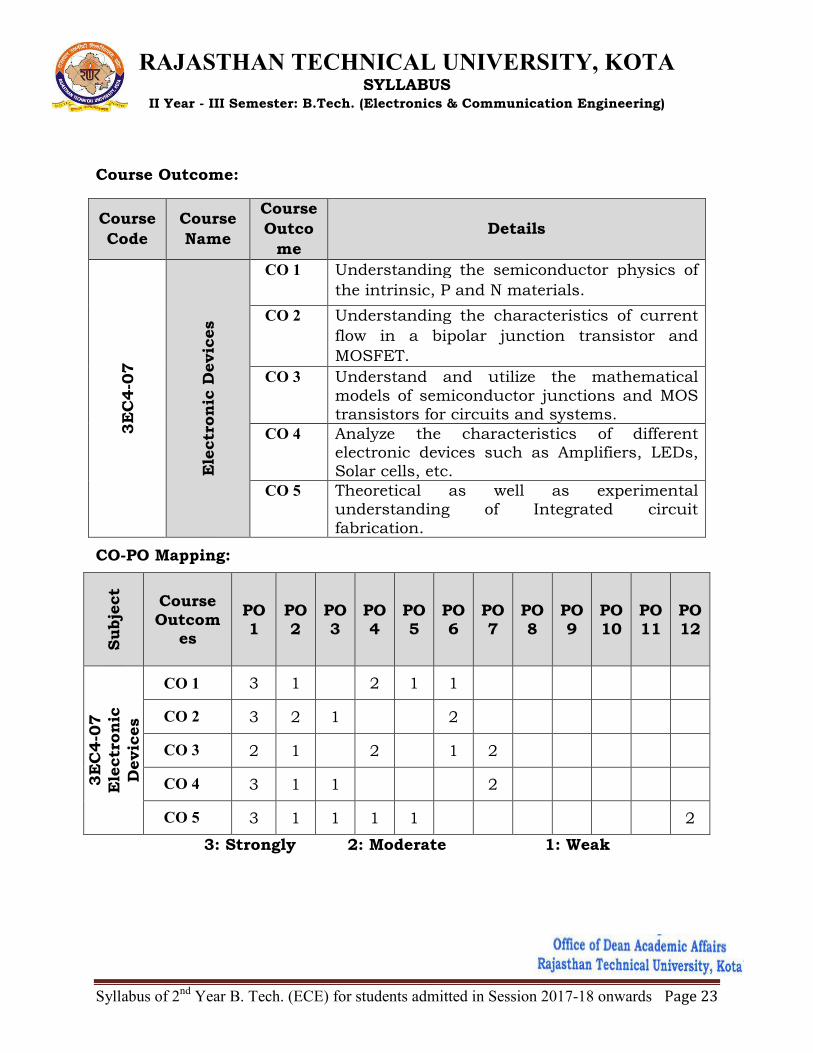
3EC4-07: Electronic Devices
4 Credits Max. Marks: 200 (IA:40, ETE:160)
3L:1T:0P End Term Exam: 3 Hours
SN Contents Hours
1 Introduction to Semiconductor Physics: Introduction, Energy band gap structures of semiconductors, Classifications of semiconductors, Degenerate and non-degenerate semiconductors, Direct and indirect band gap semiconductors, Electronic properties of Silicon, Germanium, Compound Semiconductor, Gallium Arsenide, Gallium phosphide & Silicon carbide, Variation of semiconductor conductivity, resistance and bandgap with temperature and doping. Thermistors, Sensitors.
6
2 Review of Quantum Mechanics, Electrons in periodic Lattices, E-k diagrams. Energy bands in intrinsic and extrinsic silicon; Carrier transport: diffusion current, drift current, mobility and resistivity; sheet resistance, design of resistors.
6
3 Generation and recombination of carriers; Poisson and continuity equation P-N junction characteristics, I-V characteristics, and small signal switching models; Avalanche breakdown,
Zener diode, Schottky diode.
8
4 Bipolar Junction Transistor, I-V characteristics, Ebers-Moll Model, MOS capacitor, C-V characteristics, MOSFET, I-V characteristics, and small signal models of MOS transistor, LED, photodiode and solar cell.
11
5 Integrated circuit fabrication process: oxidation, diffusion, ion implantation, Photolithography, etching, chemical vapor deposition, sputtering, twin-tub CMOS process.
9
Total 40
RAJASTHAN TECHNICAL UNIVERSITY, KOTA SYLLABUS
II Year - III Semester: B.Tech. (Electronics & Communication Engineering)
Syllabus of 2nd
Year B. Tech. (ECE) for students admitted in Session 2017-18 onwards Page 23
Course Outcome:
CO-PO Mapping:
Subje
ct
Course Outcom
es
PO 1
PO 2
PO 3
PO4
PO5
PO6
PO7
PO8
PO9
PO10
PO11
PO12
3E
C4-0
7
Ele
ctr
on
ic
Devic
es
CO 1 3 1 2 1 1
CO 2 3 2 1 2
CO 3 2 1 2 1 2
CO 4 3 1 1 2
CO 5 3 1 1 1 1 2
3: Strongly 2: Moderate 1: Weak
Course
Code
Course
Name
Course
Outco
me
Details
3E
C4-0
7
Ele
ctr
on
ic D
evic
es
CO 1 Understanding the semiconductor physics of
the intrinsic, P and N materials.
CO 2 Understanding the characteristics of current
flow in a bipolar junction transistor and
MOSFET.
CO 3 Understand and utilize the mathematical models of semiconductor junctions and MOS transistors for circuits and systems.
CO 4 Analyze the characteristics of different electronic devices such as Amplifiers, LEDs, Solar cells, etc.
CO 5 Theoretical as well as experimental understanding of Integrated circuit fabrication.

RAJASTHAN TECHNICAL UNIVERSITY, KOTA SYLLABUS
II Year - III Semester: B.Tech. (Electronics & Communication Engineering)
Syllabus of 2nd
Year B. Tech. (ECE) for students admitted in Session 2017-18 onwards Page 24
Lecture Plan:
Lecture
No.
Content to be taught
Lecture 1 Zero Lecture
Lecture 2 Introduction to Semiconductor Physics
Lecture 3 Introduction to Semiconductor Physics
Lecture 4 Introduction to Semiconductor Physics
Lecture 5 Review of Quantum Mechanics
Lecture 6 Electrons in periodic Lattices
Lecture 7 E-k diagrams
Lecture 8 Energy bands in intrinsic and extrinsic silicon
Lecture 9 Carrier transport: diffusion current, drift current, mobility and
resistivity
Lecture 10 Sheet resistance and design of resistors
Lecture 11 Generation and recombination of carriers
Lecture 12 Poisson and continuity equation
Lecture 13 P-N junction characteristics and their I-V characteristics
Lecture 14 P-N junction characteristics and their I-V characteristics
Lecture 15 P-N junction small signal switching models
Lecture 16 P-N junction small signal switching models
Lecture 17 Avalanche breakdown
Lecture 18 Zener diode and Schottky diode
Lecture 19 Basics of Bipolar Junction Transistor
Lecture 20 I-V characteristics of BJT
Lecture 21 Ebers-Moll Model
Lecture 22 MOS capacitor
Lecture 23 MOS capacitor

RAJASTHAN TECHNICAL UNIVERSITY, KOTA SYLLABUS
II Year - III Semester: B.Tech. (Electronics & Communication Engineering)
Syllabus of 2nd
Year B. Tech. (ECE) for students admitted in Session 2017-18 onwards Page 25
Lecture 24 C-V characteristics
Lecture 25 Basics of MOSFET
Lecture 26 Basics of MOSFET
Lecture 27 I-V characteristics of MOSFET
Lecture 28 Small signal models of MOS transistor
Lecture 29 Small signal models of MOS transistor
Lecture 30 Light Emitting Diode
Lecture 31 Photodiode and solar cell
Lecture 32 Basics of Integrated Circuits
Lecture 33 Advancement in Integrated Circuits
Lecture 34 Oxidation, diffusion and ion implantation
Lecture 35 Photolithography and etching
Lecture 36 Chemical vapor deposition
Lecture 37 Sputtering
Lecture 38 Twin-tub CMOS process
Lecture 39 Spill over class
Lecture 40 Spill over class
Content delivery method:
1. Chalk and Duster
2. PPT
3. Hand-outs

RAJASTHAN TECHNICAL UNIVERSITY, KOTA SYLLABUS
II Year - III Semester: B.Tech. (Electronics & Communication Engineering)
Syllabus of 2nd
Year B. Tech. (ECE) for students admitted in Session 2017-18 onwards Page 26
Sample assignments:
Assignment 1 Q1. Investigates the input/output characteristics of various diodes?
Q2. Investigate the applications of various diodes?
Q3. A p-type sample of silicon has a resistivity of 5 Ω-cm. In this sample, the hole mobility, µh, is 600
cm2/V-s and the electron mobility, µe, is 1600
cm2/V-s. Ohmic contacts are formed on the ends
of the sample and a uniform electric field is imposedwhich results in a drift current density in
the sample is 2 x 10³ A/cm
2.
[1]. What are the hole and electron concentrations in this sample?
[2]. What are the hole and electron drift velocities under these conditions?
[3]. What is the magnitude of the electric field?
Assignment 2 Q1. Discuss the applications of Ebers-Moll Model.
Q2. Discuss different types of fabrication techniques.
Q3. Discuss various characteristics of CMOS transistor.

RAJASTHAN TECHNICAL UNIVERSITY, KOTA SYLLABUS
II Year - III Semester: B.Tech. (Electronics & Communication Engineering)
Syllabus of 2nd
Year B. Tech. (ECE) for students admitted in Session 2017-18 onwards Page 27
3EC4-21: Electronics Devices Lab
1 Credit Max. Marks: 50 (IA:30, ETE:20)
0L:0T:2P
List of Experiments
Sr.
No. Name of Experiment
1.
Study the following devices: (a) Analog& digital multimeters (b) Function/
Signal generators (c) Regulated d. c. power supplies (constant voltage and
constant current operations) (d) Study of analog and digital CRO,
measurement of time period, amplitude, frequency & phase angle using
Lissajous figures.
2. Plot V-I characteristic of P-N junction diode & calculate cut-in voltage,
reverse Saturation current and static & dynamic resistances.
3.
Plot the output waveform of half wave rectifier and effect of filters on
waveform. Also calculate its ripple factor.
4. Study bridge rectifier and measure the effect of filter network on D.C.
voltage output & ripple factor.
5. Plot and verify output waveforms of different clipper and clamper.
6. Plot V-I characteristic of Zener diode
7. Study of Zener diode as voltage regulator. Observe the effect of load
changes and determine load limits of the voltage regulator
8. Plot input-output characteristics of BJT in CB, CC and CE configurations.
Find their h-parameters.
9. Study of different biasing circuits of BJT amplifier and calculate its Q-
point.
10. Plot frequency response of two stage RC coupled amplifier & calculate its
bandwidth .
11. Plot input-output characteristics of field effect transistor and measure Idss
and Vp.
12. Plot frequency response curve for FET amplifier and calculate its gain
bandwidth product.

RAJASTHAN TECHNICAL UNIVERSITY, KOTA SYLLABUS
II Year - III Semester: B.Tech. (Electronics & Communication Engineering)
Syllabus of 2nd
Year B. Tech. (ECE) for students admitted in Session 2017-18 onwards Page 28
Course Outcome:
CO-PO Mapping:
Subje
ct
Course Outcom
es
PO 1
PO 2
PO 3
PO4
PO5
PO6
PO7
PO8
PO9
PO10
PO11
PO12
3E
C4-2
1
Ele
ctr
on
ic
Devic
es L
ab
CO 1 3 2 3 2 1 1
CO 2 2 3 1 3 3 2
CO 3 2 1 2 3 3
CO 4 3 2 3 2 2 1
CO 5 3 2 1 2 2
3: Strongly 2: Moderate 1: Weak
Course
Code
Cours
e
Name
Course
Outcom
e
Details
3E
C4-2
1
Ele
ctr
on
ic D
evic
es L
ab
CO 1 Understand the characteristics of different Electronic Devices.
CO 2 Verify the rectifier circuits using diodes and implement them using hardware.
CO 3 Design various amplifiers like CE, CC, common source amplifiers and implement them using hardware and also observe their frequency responses
CO 4 Understand the construction, operation and characteristics of JFET and MOSFET, which can be used in the design of amplifiers.
CO 5 Understand the need and requirements to obtain frequency response from a transistor so that Design of RF amplifiers and other high frequency amplifiers is feasible

RAJASTHAN TECHNICAL UNIVERSITY, KOTA SYLLABUS
II Year - III Semester: B.Tech. (Electronics & Communication Engineering)
Syllabus of 2nd
Year B. Tech. (ECE) for students admitted in Session 2017-18 onwards Page 29
3EC4-22: Digital System Design Lab
1 Credit Max. Marks: 50 (IA:30, ETE:20)
0L:0T:2P
List of Experiments
S.No. Name of Experiment
Part A: Combinational Circuits
1. To verify the truth tables of logic gates: AND, OR, NOR, NAND, NOR, Ex-OR and Ex-NOR
2. To verify the truth table of OR, AND, NOR, Ex-OR, Ex-NOR logic gates realized using NAND & NOR gates.
3. To realize an SOP and POS expression.
4. To realize Half adder/ Subtractor& Full Adder/ Subtractor using NAND & NOR gates and to verify their truth tables
5. To realize a 4-bit ripple adder/ Subtractor using basic Half adder/ Subtractor& basic Full Adder/ Subtractor.
6. To design 4-to-1 multiplexer using basic gates and verify the truth table. Also verify the truth table of 8-to-1 multiplexer using IC
7. To design 1-to-4 demultiplexer using basic gates and verify the truth table. Also to construct 1-to-8 demultiplexer using blocks of 1-to-4 demultiplexer
8. To design 2x4 decoder using basic gates and verify the truth table. Also verify the truth table of 3x8 decoder using IC
9. Design & Realize a combinational circuit that will accept a 2421 BCD code and drive a TIL -312 seven-segment display
Part B: Sequential Circuits
10. Using basic logic gates, realize the R-S, J-K and D-flip flops with and without clock signal and verify their truth table.
11. Construct a divide by 2, 4 & 8 asynchronous counter. Construct a 4-bit binary counter and ring counter for a particular output pattern using D flip flop.
12. Design and construct unidirectional shift register and verify the
13. Design and construct BCD ripple counter and verify the function.
14. Design and construct a 4 Bit Ring counter and verify the function
15. Perform input/output operations on parallel in/Parallel out and Serial in/Serial out registers using clock. Also exercise loading only one of multiple values into the register using multiplexer.
Note: Minimum 6 experiments to be conducted from Part-A& 4 experiments to
be conducted from Part-B.

RAJASTHAN TECHNICAL UNIVERSITY, KOTA SYLLABUS
II Year - III Semester: B.Tech. (Electronics & Communication Engineering)
Syllabus of 2nd
Year B. Tech. (ECE) for students admitted in Session 2017-18 onwards Page 30
Course Outcome:
CO-PO Mapping:
Subje
ct
Course Outcom
es
PO 1
PO 2
PO 3
PO4
PO5
PO6
PO7
PO8
PO9
PO10
PO11
PO12
3E
C4-2
2
Dig
ital
Syste
m
Desig
n L
ab
CO 1 3 3 1 1
CO 2 3 3 2 1 1 1
CO 3 3 3 3 2 3 1 2
CO 4 3 3 3 2 3 1 2
CO 5 3 3 3 3 3 3 3
3: Strongly 2: Moderate 1: Weak
Course
Code
Cours
e
Name
Course
Outcome Details
3E
C4-2
2
Dig
ital
Syste
m
Desig
n L
ab
CO 1
CO 2 To minimize the complexity of digital logic circuits.
CO 3 To design and analyse combinational logic circuits.
CO 4 To design and analyse sequential logic circuits.
CO 5 Able to implement applications of
combinational & sequential logic circuits.

RAJASTHAN TECHNICAL UNIVERSITY, KOTA SYLLABUS
II Year - III Semester: B.Tech. (Electronics & Communication Engineering)
Syllabus of 2nd
Year B. Tech. (ECE) for students admitted in Session 2017-18 onwards Page 31
3EC4-23: Signal Processing Lab
1 Credit Max. Marks: 50 (IA:30, ETE:20)
0L:0T:2P
List of Experiments
Sr.
No. Name of Experiment (Simulate using MATLAB environment)
1. Generation of continuous and discrete elementary signals (periodic and
non periodic) using mathematical expression.
2. Generation of Continuous and Discrete Unit Step Signal.
3. Generation of Exponential and Ramp signals in Continuous & Discrete
domain.
4. Continuous and discrete time Convolution (using basic definition).
5. Adding and subtracting two given signals. (Continuous as well as
Discrete signals)
6. To generate uniform random numbers between (0, 1).
7. To generate a random binary wave.
8.
To generate and verify random sequences with arbitrary distributions,
means and variances for following:
(a) Rayleigh distribution
(b) Normal distributions: N(0,1).
(c) Gaussion distributions: N (m, x)
9. To plot the probability density functions. Find mean and variance for
the above distributions
Course Outcome:
Course
Code
Course
Name
Course
Outcom
e
Details
3E
C4-2
3
Sig
nal
Pro
cessin
g L
ab CO 1 Able to generate different Continuous and Discrete time signals.
CO 2 Understand the basics of signals and different operations on signals.
CO 3 Develop simple algorithms for signal processing and test them using MATLAB
CO 4 Able to generate the random signals having different distributions, mean and variance.
CO 5 Design and conduct experiments, interpret and analyse data and report results.

RAJASTHAN TECHNICAL UNIVERSITY, KOTA SYLLABUS
II Year - III Semester: B.Tech. (Electronics & Communication Engineering)
Syllabus of 2nd
Year B. Tech. (ECE) for students admitted in Session 2017-18 onwards Page 32
CO-PO Mapping: Subje
ct
Course Outcom
es
PO 1
PO 2
PO 3
PO4
PO5
PO6
PO7
PO8
PO9
PO10
PO11
PO12
3E
C4-2
3
Sig
nal
Pro
cessin
g
Lab
CO 1 2 1 2
CO 2 3 1
CO 3 1 2 3 1 3
CO 4 2 1 1 2
CO 5 1 1 2 2 2
3: Strongly 2: Moderate 1: Weak

RAJASTHAN TECHNICAL UNIVERSITY, KOTA SYLLABUS
II Year - III Semester: B.Tech. (Electronics & Communication Engineering)
Syllabus of 2nd
Year B. Tech. (ECE) for students admitted in Session 2017-18 onwards Page 33
3EC3-24: Computer Programming Lab-I
1 Credit Max. Marks: 50 (IA:30, ETE:20)
0L:0T:2P
1. Write a simple C program on a 32 bit compiler to understand the concept of
array storage, size of a word. The program shall be written illustrating the
concept of row major and column major storage. Find the address of
element and verify it with the theoretical value. Program may be written for
arrays upto 4-dimensions.
2. Simulate a stack, queue, circular queue and dequeue using a one
dimensional array as storage element. The program should implement the
basic addition, deletion and traversal operations.
3. Represent a 2-variable polynomial using array. Use this representation to
implement addition of polynomials.
4. Represent a sparse matrix using array. Implement addition and
transposition operations using the representation.
5. Implement singly, doubly and circularly connected linked lists illustrating
operations like addition at different locations, deletion from specified
locations and traversal.
6. Repeat exercises 2, 3 & 4 with linked structures.
7. Implementation of binary tree with operations like addition, deletion,
traversal.
8. Depth first and breadth first traversal of graphs represented using
adjacency matrix and list.
9. Implementation of binary search in arrays and on linked Binary Search
Tree.
10. Implementation of insertion, quick, heap, topological and bubble sorting
algorithms.