taher ghomian, hyunhak jeong, victor pan, kubra celik
TRANSCRIPT

www.advmatinterfaces.de
2001476 (1 of 10) © 2021 Wiley-VCH GmbH
Full PaPer
High-Throughput Dielectrophoretic Trapping and Detection of DNA Origami
Taher Ghomian, Hyunhak Jeong, Victor Pan, Kubra Celik, Mashari Alangari, Yonggang Ke, and Joshua Hihath*
DOI: 10.1002/admi.202001476
1. Introduction
Recently, nanomaterials are increas-ingly being used in many applica-tions such as electronics,[1–3] biology,[4] energy harvesting,[1,5–7] agriculture,[8] optoelectronics,[1,9] and chemistry.[10] Deoxyribonucleic acid (DNA), beyond its key function in biology as a long-term memory of genetic information and instruction, has arisen as a promising nanomaterial, and it is being widely used in many interdisciplinary fields of nano-technology such as nanoelectronics.[11–14] DNA possesses unique electronic,[15] mechanical,[16] biological,[17] and physical[18] properties providing an excellent platform for potentially developing compact, high throughput, flexible, robust, and low-cost electronic devices. Another significant advantage of DNA is its exceptional self-assembly properties which open up a novel opportunity for the bottom-up design and fabrication of nanoscale devices[19] with resolutions that can surpass conven-
tional lithographic technologies. In particular, it is possible to build exceptionally complex nanostructures by folding long DNA strands into desired 2D or 3D shapes at nanometer scales. These artificial DNA nanostructures are often referred to as “DNA origami.”[20] This can realize a further step toward scaling down of tunable electronic devices and circuits as well as high-density memory devices which are beyond the limit of conventional silicon technology.[21,22]
Therefore, the study of the properties of DNA is in the interest of science and engineering. In order to study the elec-trical and mechanical properties of DNA nanostructures, to analyze the behavior of the DNA structures in specific chem-ical environments, and to integrate DNA nanostructure into a large-scale system, it is necessary to confidently and precisely attach and immobilize the DNA nanostructures to prede-fined locations within a device structure. Moreover, effective manipulation of DNA nanostructures is important since DNA origamis are expensive to produce and typically supplied in small volumes on the order of microliters with a low concentration (× 10–9 m).
Several methods are available for guiding, trapping, and immobilizing DNA nanostructures at the location of interest. Optical trapping as a noninvasive technique has been widely studied for manipulating micro- and nano-materials for
Accurate control over the location of nanostructured materials for studying their electronic properties is important for the development of useful elec-tronic devices. Dielectrophoresis is a unique method for trapping non-symmetric nanostructured materials between two electrodes in a specific direction. However, this method has traditionally suffered from a costly and slow fabrication process as well as low efficiency when trapping high-imped-ance nanomaterials. In this work, a dielectrophoretic device addressing the mentioned problems, is reported. First, a photolithography-based fabrication process achieves high throughput and low-cost devices with nanostructured contacts for attaching nanomaterials. Second, trapping of high-impedance nanomaterials is controlled using a scalable-electronic circuit that measures the capacitance variation at the trap location to identify when the nanomate-rials of interest are attached to the electrode. As a primary target of interest, the trapping of 1D deoxyribonucleic acid (DNA) origamis is demonstrated. It is shown that a capacitance change in the range of 18% to 60% guarantees the presence of a single or a few DNA origamis in the trap location well-aligned with nanoelectrodes. Fluorescent, scanning electron microscopy, and atomic force microscopy images demonstrate the presence of DNA origamis in the trap location with the correct orientation.
Prof. T. Ghomian, Dr. H. Jeong, Prof. K. Celik, M. Alangari, Prof. J. HihathDepartment of Electrical and Computer EngineeringUniversity of CaliforniaDavis, CA 95616, USAE-mail: [email protected]. T. GhomianDepartment of Computer Sciences and Electrical EngineeringMarshall UniversityHuntington, WV 25755, USADr. V. Pan, Prof. Y. KeDepartment of Biomedical EngineeringGeorgia Institute of Technology and Emory UniversityAtlanta, Georgia 30322, USAProf. K. CelikCivil Aviation CollegeDepartment of Air Traffic ControlFirat UniversityElazig 23180, TurkeyM. AlangariElectrical Engineering DepartmentUniversity of Ha’ilHa’il 81451, Saudi Arabia
The ORCID identification number(s) for the author(s) of this article can be found under https://doi.org/10.1002/admi.202001476.
Adv. Mater. Interfaces 2021, 8, 2001476

www.advancedsciencenews.com
© 2021 Wiley-VCH GmbH2001476 (2 of 10)
www.advmatinterfaces.de
biomedical applications.[23,24] In this method, a focused laser beam applies a high optical gradient force to confine the par-ticle at a focal point. Optical tweezers can be integrated on a chip providing useful devices for simultaneously running mul-tiple tests as well as high throughput fabrication devices. How-ever, optical tweezers suffer from low efficiency and operation is hard especially when they are dealing with nanomaterials. To improve the efficiency of this method, some measurements are required such as incorporating plasmonic structures[25] which increases the cost and complexity of the fabrication process. Another feasible approach for nanomaterial confinement is based on the hydrodynamic flow in a microfluidic structure.[26] In this method, the position of the particle is adjusted by con-trolling the fluid flow in a simple cross-slot channel. Using this method, Tanyeri et al. demonstrated a low-cost, highly efficient, and easy to operate method for trapping and manipulation of spherical micro- and nano-materials. However, control-ling the location of the nanomaterials without 3D symmetry such as DNA origamis or non-spherical cells is challenging with this method since the orientation of the nanomaterial is important in adjusting the parameters. As another method, Lil-liehorn et al. showed that the interaction of nanomaterials with acoustic waves inside a microfluidic channel can trap the nano-materials in a specific location. In particular, nanomaterials are placed in pressure minima of standing ultrasonic waves gen-erated through the channel.[27] Although this method provides good control and fast method for locating nanomaterials in a micrometer size trap location, it could damage the nanomate-rial and operation is not simple.
The methods discussed above have focused mostly on manipulating nanomaterials such as sorting or trapping inside the solution. However, for studying the electrical properties of a trapped nanomaterial, further capabilities are required in order to align the nanomaterials in a specific direction (espe-cially for non-spherical nanomaterials) and electrically connect them to a pair of electrodes, then immobilize them in that loca-tion. Nanomaterial trapping based on the electrical field is a promising method to manipulate nanomaterials for trapping them in a precise location and desirable orientation.[28–33] This also provides the advantage of studying the electrical proper-ties of the nanomaterial. This trapping mechanism is based on dielectrophoresis (DEP) phenomena generated by conductive micro- or nano-electrodes. Dielectrophoresis is a phenomenon in which a polarizable particle moves when it is placed in a non-uniform electric field.[34] The force that moves the particle can be toward or against the high intensity region of the elec-tric field depending on the dielectric properties of the particle. This phenomenon plays an important role in biological diag-nostics for separating, sorting, fractioning, and concentrating biological samples because it is fast, noninvasive, and nonde-structive.[35] In addition, DEP only requires a small volume of sample allowing faster and massively parallel manipulation as well as facilitating analysis of electrical, mechanical, and biolog-ical functions in a miniaturized device.[35] However, nanomate-rial manipulation relying on DEP requires fabrication of at least a pair of specific conductive electrodes fitting the dimension of the targeted nanomaterial. A few experimental demonstra-tions have reported DNA origamis trapping using dielectro-phoresis phenomena. Kuzyk et al. proposed a DEP device
fabricated by electron beam lithography on a SiO2 substrate for trapping 2D DNA origamis. They control the trap mechanism by tuning the buffer concentration, applied voltage level, and frequency.[36] They reported 10% efficiency in precisely trapping the origamis in between the electrodes. In other research, Shen et al. reported a DEP structure on a silicon dioxide substrate. They demonstrated anchoring different shapes of 3D DNA origamis to fabricated 20-nm-thick gold nanoelectrodes with a yield of higher than 50%.[28]
To the best of our knowledge, the DEP devices used for trap-ping nanomaterials incorporate high cost and low throughput electron beam lithography for nanoelectrode fabrication on a silicon dioxide (SiO2) substrate. The hydrophilic properties of the SiO2 surface provide a reliable surface for attaching DNA origamis, and the insulating properties of this substrate are also suitable for conducting I–V measurements on high-impedance origamis. However unexpected destruction by the formation of a nanocanyon between the electrodes during the trapping procedure is observed on the SiO2 substrate.[28] In addition, the presented DEP devices lack effective monitoring of the trap-ping mechanism. The trap mechanism is generally tuned based on the applied voltage level, frequency of the signal, solution concentration, and trap time. Since there is an unavoidable dif-ference in each experimental condition such as the geometry of the nanoelectrodes on different chips or solution molarity of different samples (especially in the case of ultra-low concentra-tion of DNA origami samples), trapping based on the prede-fined parameters results in low yield. This can be even worse if there is a slight modification on either device fabrication or sample preparation processes.
The goal of this work is to present a reliable method to precisely trap the DNA origamis, dispersed in the solution, between a pair of nanoelectrodes and address the mentioned problems associated with both costly fabrication process and lack of trap monitoring mechanism. This method involves high throughput fabrication process, surface preparation, and spe-cific electronic circuit designed for trapping and monitoring. A 1D 10-Helix-Bundle (10HB) DNA origami with ≈1250 nm in length are assembled from five ≈250 nm monomers and then used for the trapping demonstration. These 10HB origamis are modified with thiols on both ends to enforce the longitudinal orientation of the origami in the trap location while attaching to the gold nanoelectrodes of the device. The thin and long structure of these DNA origamis makes the trapping and moni-toring challenging because it usually demands very thin elec-trodes (cross-section area of less than 10 nm × 10 nm) to pre-vent aggregation of DNA origamis in between the electrodes. In addition, this 1D DNA origami is an ultra-high impedance nanomaterial therefore detecting the presence of it in the trap location is another challenge.
2. Results
2.1. Device Structure
The device structure consists of two thin gold nanoelectrodes connected to contact pads through gold wires on a sapphire substrate as shown in Figure 1a. The high insulation property of
Adv. Mater. Interfaces 2021, 8, 2001476

www.advancedsciencenews.com
© 2021 Wiley-VCH GmbH2001476 (3 of 10)
www.advmatinterfaces.de
the sapphire substrate makes it an excellent candidate for high impedance measurements at high frequencies. This is not the case for SiO2 substrate since the Si layer beneath the oxide layer conducts current at high frequencies and increases the limit of conductance measurement. The width of one nanoelectrode is ≈400 nm and the width of the other one is 600 nm. The asym-metrical structure of the electrodes generates enhanced electric field gradient in between the electrodes; therefore, DEP force enhances in the space between the electrodes.[37] Accordingly, lower voltage is required to guide the DNA origami toward the trap location which decreases the leakage current and improves the accuracy of the measurement. The height of the electrodes is ≈65 nm. Although it is possible to deposit thinner electrodes to have precise control on monitoring the trap, the visual con-trol and fluorescent imaging of such a thin device on a trans-parent sapphire substrate is difficult. Since the monitoring circuit worked well with 65-nm-height nanoelectrodes, we didn’t decrease the thickness of the gold nanoelectrodes. The optical image of the fabricated chip is shown in Figure 1b. This chip consists of 14 devices with three trap sizes including 400, 600, and 800 nm. Scanning electron microscopy (SEM) image in Figure 1c shows that the trap area is not encapsulated with a silicon nitride insulator layer and opened for electrical con-nection to electrodes. The AC electric field in between the two gold substrates attracts DNA origamis toward the high-intensity region of the electric field. Since the length of our DNA ori-gami (1250 nm) is much longer than the gap sizes on a chip,
all DEP devices on the chip are suitable for trapping purposes. To reduce the cost and increase the throughput of the fabri-cation process, projection photolithography is used instead of the commonly used electron-beam lithography technique. The minimum achievable device dimension with photolithog-raphy is related to the wavelength of the exposure source used for recording the pattern of a mask on to the photoresist. The exposure source of GCA Wafer Stepper is 365-nm UV light, therefore, 400-nm feature is reachable. Although e-beam lithog-raphy can pattern much smaller dimensions, its costs and low throughput hinder its use for applications. As such, we have designed a monitoring circuit to address the drawbacks associ-ated with the wider nanoelectrodes obtained using photolithog-raphy (see below). The fluorescent image, shown in Figure 1c, illustrates the presence of DNA origami trapped between the nanoelectrodes.
2.2. Fabrication Process and Surface Preparation
The overview of the fabrication process of the dielectrophoresis chip is shown in Figure 2a. 270-nm-thick high-resolution posi-tive photoresist (KL 5302) is spin-coated on a clean sapphire wafer. Then, the wafer is soft baked to remove the solvent from the photoresist layer. After this step, the wafer is exposed to the UV light through a designed mask for an optimum dose. The process is followed by one more step of soft baking and then developing in MF CD-26 to remove the exposed areas on the photoresist. Then 5/60-nm-thick Cr/Au metals are deposited on the device with an e-beam evaporator. The thin layer of chromium gives a good adhesion of gold on the sub-strate. The fabrication process is followed by a lift-off process to remove all the unwanted photoresists and metallic layers. In order to have a better control of the trapping process in terms of the trap location and monitoring, all the connections on the chip are covered with an insulating layer and only the trap area is exposed to the DNA origami solution. Therefore, a 100-nm thick silicon nitride (Si3N4) layer is deposited on the entire surface of the chip using PECVD. To define the open areas, standard photolithography methods are employed. 1 µm-thick positive photoresist (S1813) is spin-coated on the silicon nitride layer. Then, the wafer is soft baked to remove the solvent from the photoresist layer. After this step, the wafer is exposed to the UV light through a designed mask for an optimum dose. The process is followed by soft baking and developing in MF CD-26 to remove the exposed areas on the photoresist. Then, the Si3N4 layer at defined areas is removed with ICP etching method. Finally, the chip is ready after a simple wet cleaning process to remove the photoresist residue and other organics left on the chip during the fabrication process.
Single crystalline sapphire (0001) surfaces contain hydro-phobic regions formed inside hydrophilic areas.[38] Therefore, the sapphire surface does not exhibit good adhesion to DNA ori-gamis, and origamis are more likely to displace with small tur-bulence. Accordingly, the sapphire surface should be functional-ized to improve the hydrophilicity of the surface. 3-Aminopropyl triethoxysilane (APTES) is a widely used coupling agent for covalently binding biomaterials to inorganic surfaces.[39] As such, careful studies have been conducted on functionalizing
Figure 1. Dielectrophoretic chip for trapping DNA origami. a) Device schematic structure of a dielectrophoresis chip on a sapphire substrate. Generated AC electric field in between gold nanoelectrodes absorbs DNA origamis to the high-intensity region of electric field and immobilizes it in a specific direction by binding the thiol linkers of DNA origami to gold electrodes; b) Optical image of a fabricated chip on a sapphire substrate including 14 devices; c) SEM image of a typical device on the chip showing gold nanoelectrodes and nitride encapsulation; and d) Fluorescent image of a device with DNA origamis trapped between nanoelectrodes.
Adv. Mater. Interfaces 2021, 8, 2001476

www.advancedsciencenews.com
© 2021 Wiley-VCH GmbH2001476 (4 of 10)
www.advmatinterfaces.de
different surfaces with APTES. Liquid-phase deposition of APTES on the sapphire surface is used to improve the adhesion of DNA origamis to the surface.[40] Figure 2b shows the silaniza-tion procedure. The process starts with chemically cleaning the fabricated dielectrophoresis chip and immersing in 20 × 10–3 m HNO3 for 30 min at room temperature. This step attaches OH groups on the surface of sapphire. The process continues by rinsing with ultra-pure DI water and drying with a nitrogen gun. Then the device is immersed in 600 × 10–3 m solution of APTES in toluene overnight inside a glovebox filled with inert gas. The process resumes by rinsing the device with toluene and tetrahydrofuran to remove excess unbounded APTES on the surface. Finally, after drying the sample with a nitrogen gun, the chip is heated at 150 °C for 2 h on a hotplate.
2.3. Theory and Simulation
The dielectrophoretic force is determined by:
1
2DEP
2F Eα ( )= ⋅ ∇ (1)
where α is the polarizability of the object and E is the root mean square value of the electric field. The finite element method (FEM) is used to determine the electric field inten-sity distribution in the area of the trap location by solving Poisson’s equation with COMSOL. Figure 3a shows the SEM image of a typical device used for trapping DNA origami with about 800 nm of separation between the 65-nm-thick nanoelectrode on the sapphire substrate. The width of each electrode is 429 and 600 nm. The electric field simulation for this chip with 1 volt applied potential, shown in Figure 2b, illustrates that intensity in the gap area is high and decreases when farther away.
In order to check the validity of the simulation, the capaci-tance value of the gap area obtained from both experimental and simulation results are compared. The experimental result shows a capacitance value of 4.57 fF for the blank chip in excellent agreement with the simulation result of 5.00 fF. Then, after applying diluted solution (16.7 × 10⁻¹² m of DNA concen-tration) to the chip, the experimental result shows that the capacitance increases from 4.57 fF of the blank chip to 165 fF. Based on our experimental results, the permittivity of the diluted solution is very close to that of DI water permittivity εr = 79.38 at 22 °C. The simulated capacitance value is 154.78 fF, again in good agreement with the measurement. Therefore, the results confirm the validity of the simulation.
In order for a DNA origami to be trapped in between the electrodes, DEP potential energy UDEP = −αE2/2[41] should be higher than the drag force of the thermal energy UTH = 3/2kB T associated with Brownian motion. Accordingly, the parameter of successful trapping is not only dependent on the electric field intensity but also on the polarizability of the DNA origami. In the solution phase, counterions are associated with the DNA backbone to neutralize the negative charge. The electric field can distort this “counterion cloud”, separate the charges, and generate dipoles.[42,43] Therefore, the presence of the counterion cloud around the DNA origami in buffer solution significantly increases the polarizability of DNA origamis. Accordingly, In the solution, DNA presents a high dielectric constant which is proportional to the length of the DNA.[43,44] The induced dipole is in the direction of the DNA’s long axis.[44]
The typical number for the polarizability of DNA equals α = 10−34Fm2/bp[32] giving UDEP = 1.147 × 10⁻¹¹E2 [ev] for the 36 760 bp DNA origamis (10 Helix bundle, 1250 nm in length) used in our experiment. Figure 3c shows the DEP potential energy along the axis perpendicular to the axis of the nano-electrodes in the middle of the gap for different heights from the surface of the substrate, shown in the insets of Figure 3c. This DEP potential energy is generated by applying 1 volt to the same electrodes with an 800 nm gap size. Generally, Figure 3c shows that the DEP potential is maximum in the center of the plot meaning the DEP potential is maximum along the direction of nanoelectrodes forcing DNA origami to bridge the nanoelectrodes. In addition, this figure shows that as moving up from the surface of the substrate, DEP poten-tial decreases. In some point higher than 2µm in height, DEP potential is close to the thermal potential (dashed line
Figure 2. Dielectrophoretic chip fabrication. a) Fabrication process of the dielectrophoresis chip on a sapphire substrate; b) Surface preparation for improving the hydrophilicity of the sapphire substrate with APTES molecules.
Adv. Mater. Interfaces 2021, 8, 2001476

www.advancedsciencenews.com
© 2021 Wiley-VCH GmbH2001476 (5 of 10)
www.advmatinterfaces.de
in Figure 3c). This means that applying the DEP signal with a peak voltage of 1 V can effectively overcome Brownian
motion force at room temperature for DNA origamis located less than 2 µm above the gap and attract them toward the trap location.
2.4. Measurement and Trap Procedure
DNA origami stock solution is composed of 100 picomolar (× 10–12 m) DNA origamis in a buffer solution. The buffer solution is 0.5xTBE (2.5 × 10⁻³ m Tris, 45 × 10–3 m boric acid, 5 × 10⁻³ m EDTA) with 10 × 10–3 m magnesium chloride. Each DNA origami is decorated with 85 covalently-linked fluoro-phores along the entire length of the wire for taking fluores-cent images. DC measurements show the resistance of the buffer solution covering the nanoelectrodes on the fabricated chip is more than 1013 Ω. Also, the resistance of both blank chip and DNA crossing the nanoelectrodes is more than 1014 Ω which is not in the measurement range of our device. Therefore, direct, DC resistance measurements do not provide useful information for the trapping mechanism. As mentioned above, the existence of the counterion cloud around the DNA origami in buffer solution substantially increases the polariz-ability of DNA origamis resulting in a high dielectric constant. Since the electric permittivity of DNA is higher than DI water for a wide range of frequencies, the presence of DNA origamis at the trap location increases the capacitance of the device.[45,46] Accordingly, the monitoring system for detecting the presence of DNA origamis in the trap location is based on capacitance measurements.
Just before the trap procedure, the stock solution is diluted in ultra-pure DI water to make a working solution with 10 × 10–12 m to 20 × 10–12 m DNA origami concentration. During the experi-ment, the chip is located inside a probe station. The metallic enclosure of probe station effectively grounds any electromag-netic noise and protects the DNA origamis from the ambient light to preserve fluorophores for fluorescent imaging. The trap procedure starts with pipetting 10 µL of prepared working solu-tion to the area of nanoelectrodes on the DEP chip while the chip is connected to the trapping circuit through a probe station. An overview of the tapping circuit is shown in Figure 4a. This circuit applies a sinusoidal signal to the nanoelectrodes of the DEP chip. Based on our experiment, the DNA origamis show higher polarizability at 6 MHz frequency, therefore working at this frequency makes the monitoring and trapping mechanism more efficient. The maximum peak voltage value of the applied signal is limited to 1 volt to prevent any unwanted reaction in the solution or any other accidental damage resulting from high electric field intensity generated between nanoelectrodes. Then, the desired trapping signal at 6 MHz with 1-volt peak value is applied to the electrodes and reads the current passing through the nanoelectrodes. The current signal is converted to a voltage with a trans-impedance amplifier and it is then amplified to improve the signal to noise ratio. Next, a lock-in technique is designed to detect the desired sinusoidal 6 MHz signal (which is at the same frequency of the applied trapping signal) combined with environmental noise. Finally, a last stage amplifier improves the signal level and sends it to LabView for storage and monitoring. While the trapping mechanism is running, the capacitance change is monitored and stored. Trap
Figure 3. Modeling dielectrophoretic trapping. a) SEM image of the DEP device with 800 nm gap size on a sapphire substrate used for modeling; b) Electric field intensity distribution around the gap at 300 nm above the substrate showing suitable pattern for trapping and aligning the DNA ori-gami; c) Potential energy along the axis perpendicular to the direction of the nanoelectrodes in the center of the gap for 50, 300, 500, 1000, and 2000 nm above the substrate surface; insets showing the measurement location.
Adv. Mater. Interfaces 2021, 8, 2001476

www.advancedsciencenews.com
© 2021 Wiley-VCH GmbH2001476 (6 of 10)
www.advmatinterfaces.de
mechanism manually stops by removing the trap signal when the signal level reaches to the specific value discussed below.
The circuit response to the capacitance value of the DEP device is simulated with MATLAB. Figure 4b shows that the output voltage is almost nearly a linear function of the device capacitance for values smaller than the 10 pF. Since our DEP device capacitance varies from a few femtofarads to sub-pico-farad, output voltage variation is almost linearly proportional to the capacitance variation. Since the decision is made based on the capacitance change, the unwanted effects of parameters such as concentration and volume of the working solution, the voltage level of the trapping signal, and nanoelectrodes geo-metry, significantly decreases in analysis. Lastly, in order to visualize the presence of the DNA origamis in the trap area,
SEM, atomic force microscopy (AFM), and fluorescent imaging techniques are used.
2.5. Characterization
One of the methods that we used for characterizing the presence of DNA origamis in the trap location is fluorescent microscopy. After finishing the trap procedure, the probes were lifted up and we waited a few minutes for the turbulences to settle down and let the DNA origamis or aggregated DNAs to be immobilized on the substrate. Then we gently covered the surface of the chip with a coverslip, and imaged the chip with fluorescence micros-copy. The intensity of the DNA origamis is used to estimate the number of DNA origamis in the trap location. However, the fluorescent intensity of fluorophores attached to DNA origamis varies depending on the exposure time and intensity of excita-tion source, solution age, and exposure time to ambient air and ambient light. In order to eliminate the effects of the excita-tion source on the intensity of the DNA origami and gain more insight into the possible variation of the intensity affecting from other mentioned factors, an image processing program was designed to calculated the normalized intensity of the DNA origami versus substrate intensity.
Therefore, the first step for characterizing the presence of DNA origami is to find possible intensity variation of a single DNA origami in the experimental conditions. A diluted working solu-tion with 10 × 10–12 m concentration is drop-cast on multiple clean sapphire substrate and fluorescent images of individual DNA origamis is captured. As demonstrated in Figure 5a, the image analysis of 12 samples shows that normalized fluorescent inten-sity of a DNA origami on a sapphire substrate varies by ≈82%. Moreover, DNA aggregates, which can form in the working solution or during the trapping process, might also be trapped between the nanoelectrodes. The normalized fluorescent intensity of eight samples containing aggregated DNA, shown in Figure 5a, varies by 55% and the average value is almost nine times that of a single DNA origami. As such, normalized fluorescent intensity of a single DNA origami has no overlap with that of aggregated DNAs for all the samples prepared in a variety of imaging, trap-ping, and solution conditions. Therefore, image processing of flu-orescent intensity can effectively distinguish between aggregated and non-aggregated DNA origamis on a sapphire substrate.
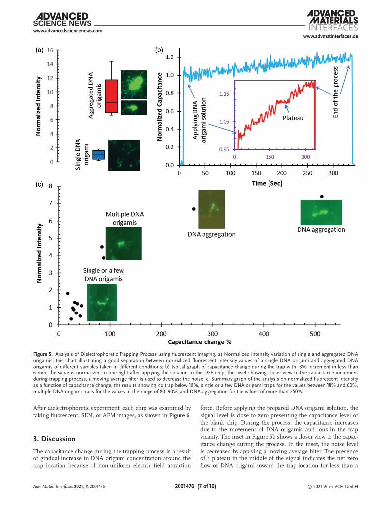
As mentioned above, many parameters affect the initial capacitance values for each device such as nanoelectrode geom-etry, the working solution concentration and volume, and the gap geometry and uniformity. To decrease the effects of the variation of these parameters on our results, trapping success is determined by measuring the normalized capacitance change for a given device (ΔC/Ci) while the RF field is applied. Ci is the initial capacitance value right after applying the working solution and ΔC is the capacitance change during the pres-ence of trapping signal. In order to find a reliable range for the capacitance change corresponding to a successful trap, different experiments are conducted. Each experiment corre-sponds to a different value of ΔC/Ci. Figure 5b shows a typ-ical trap monitoring signal corresponding to an 18% increase in the capacitance during a course of 6 min trapping proce-dure, which results in the successful placement of origami.
Figure 4. Dielectrophoretic trapping circuit. a) Circuit block diagram of the trapping and monitoring device. The circuit applying a sinusoidal signal to the dielectrophoresis chip and reading the current. The cur-rent which is proportional to the capacitance of the DEP chip is ampli-fied, filtered, stored, and monitored; b) Output voltage of the circuit is almost linearly proportional to the capacitance of the device in the range of interest (less than 10 pF).
Adv. Mater. Interfaces 2021, 8, 2001476
www.advancedsciencenews.com
© 2021 Wiley-VCH GmbH2001476 (7 of 10)
www.advmatinterfaces.de
After dielectrophoretic experiment, each chip was examined by taking fluorescent, SEM, or AFM images, as shown in Figure 6.
3. Discussion
The capacitance change during the trapping process is a result of gradual increase in DNA origami concentration around the trap location because of non-uniform electric field attraction
force. Before applying the prepared DNA origami solution, the signal level is close to zero presenting the capacitance level of the blank chip. During the process, the capacitance increases due to the movement of DNA origamis and ions in the trap vicinity. The inset in Figure 5b shows a closer view to the capac-itance change during the process. In the inset, the noise level is decreased by applying a moving average filter. The presence of a plateau in the middle of the signal indicates the net zero flow of DNA origami toward the trap location for less than a
Figure 5. Analysis of Dielectrophoretic Trapping Process using fluorescent imaging. a) Normalized intensity variation of single and aggregated DNA origamis, this chart illustrating a good separation between normalized fluorescent intensity values of a single DNA origami and aggregated DNA origamis of different samples taken in different conditions; b) typical graph of capacitance change during the trap with 18% increment in less than 6 min, the value is normalized to one right after applying the solution to the DEP chip; the inset showing closer view to the capacitance increment during trapping process, a moving average filter is used to decrease the noise. c) Summary graph of the analysis on normalized fluorescent intensity as a function of capacitance change, the results showing no trap below 18%, single or a few DNA origami traps for the values between 18% and 60%, multiple DNA origami traps for the values in the range of 80–90%, and DNA aggregation for the values of more than 250%.
Adv. Mater. Interfaces 2021, 8, 2001476

www.advancedsciencenews.com
© 2021 Wiley-VCH GmbH2001476 (8 of 10)
www.advmatinterfaces.de
minute. This might be attributed to the presence of induced backflow in the solution,[47,48] or potentially the trapping of an origami structure. Finally, after reaching to the desired capaci-tance value, the process stops by removing the trapping signal. A fluorescent image was taken after each trap, and the fluo-rescence intensity between the nanoelectrodes was recorded for processing purpose. Figure 5c summarizes the analysis results showing normalized fluorescent intensity as a function of capacitance change for 13 experiments. There is a low chance of successful DNA origami trapping for the capacitance changes of less than 18% and more than 250% at the normal trapping time of ≈6 min. The capacitance changes below 18% are attributed to the concentration increase due to the migra-tion of DNA origamis into the electrode area without binding. On the other hand, capacitance changes of more than 250% are attributed to the presence of aggregated DNAs or other con-taminating structures within the nanogap. Image processing shows the normalized fluorescence intensity of this category is in the range of values for DNA aggregation discussed above and shown in Figure 5a. Figure 6d,e illustrates the fluorescent image and corresponding SEM image of aggregated DNAs on a chip, respectively, with capacitance change of 513% and nor-malized fluorescent intensity of more than seven.
Thus, the important features for trapping DNA origamis occur between these two extremes. Capacitance changes in the range of 18% to 60% correspond to the normalized fluorescent
intensity of less than 1.8 suggesting one or only a few DNA origamis in the gap. Clear fluorescent images of a few trapped DNA origamis in Figure 6a,b as well as AFM and SEM images of a single DNA origami of a chip in Figure 6f,g illustrate the presence of single or a few DNA origamis for devices measured in this capacitance range.
Another category in Figure 5c is related to the capacitance change in the range of 80% to 90%. Samples in this area present normalized fluorescent intensity four times the average intensity of a single origami. Moreover, the samples of this cat-egory are separated well from the other categories. This cannot be categorized in the single or a few DNA origami because of higher normalized fluorescent intensity. However, the intensity is much less than aggregated DNA origamis. The fluorescent image of one sample in the category is presented in Figure 6c showing straight and very bright fluorescent intensity sug-gesting that many DNA origamis are well-aligned in the gap between electrodes.
Fluorescent intensity and capacitance values vary depending on many parameters during the synthesis process, trap proce-dure, and imaging condition. However, using the normalized values to analyze the data allows for a reliable methodology for identifying successful traps of DNA origamis down to the few-DNA level. We find there is one or only a few DNA ori-gamis trapped between the nanoelectrodes if the capacitance change is between 18% to 60%. If the aggregated DNA cluster
Figure 6. Imaging dielectrophoretically trapped structures. a,b) Fluorescent images presenting a few (likely two) trapped DNA origamis between nano-electrodes on two different chips; only a part of nanoelectrodes which are under the nitride layer is clearly visible c) High intensity fluorescent image showing multiple trapped DNA origamis aligned well along the nanoelectrodes; d) Fluorescent and e) SEM images of the same device illustrating aggregated DNA cluster trapping in between two nanoelectrodes; f) SEM and g) AFM phase images of the same chip presenting a single DNA origami immobilized along the nanoelectrodes.
Adv. Mater. Interfaces 2021, 8, 2001476

www.advancedsciencenews.com
© 2021 Wiley-VCH GmbH2001476 (9 of 10)
www.advmatinterfaces.de
is trapped between nanoelectrodes, normalized capacitance increases to higher values such as 250% or more within the normal trap time. Also, it is possible to detect multiple DNA origamis trapped in between nanoelectrodes corresponding to the capacitance change in the range of 80% to 90%. Based on our experiments, a trap time of ≈6 min for concentrations of 10–20 × 10–12 m and with an applied signal of 1 V yields con-sistent and reliable trapping.
4. Conclusion
This paper presents a low-cost, high-throughput dielectropho-retic platform for trapping and monitoring high impedance polarizable nanostructures such as DNA origami. Photolithog-raphy method is used to fabricate the dielectrophoretic chips providing fast and low-cost fabrication process. The device is used to trap 1D DNA origami wires, and we demonstrate that the method is capable of distinguishing between aggregated DNAs and down to a few DNAs in the trap location with a high sensitivity capacitance measurement. The results show that a capacitance change in the range of 18% to 60% is highly indicative of the presence of only a few DNA origamis in the trap location, but that values greater than 250% indicate that aggregation has occurred. Moreover, it is possible to trap mul-tiple DNAs in the designated location by increasing the trap time and monitoring the capacitance change. For instance, at an 80% to 90% capacitance change, multiple DNA origamis are always present in the trap location, and still aligned with nanoelectrodes. The normal time to trap a single or a few DNA origamis is around 6 min for our experimental conditions. This method is applicable to all types of polarizable micro- and nano-materials even for the high-impedance materials with non-symmetric structures such as DNA origamis. This highly-scalable methodology could allow trapping of a wide variety of different types of nanomaterials including biological molecules and carbon nanotubes for fabricating solution-processed cir-cuits, devices, and high density memories. Furthermore, this method can be used to parallelize the trapping process in a pre-defined electrode array allowing high-throughput device fabri-cation with selective deposition of nanomaterials.
5. Experimental SectionDNA Origami Preparation Method: In selecting an origami structure to
be the basis of the nanowire, the 10 helix bundle nanorod was chosen for its improved rigidity and persistence length compared to longer origamis with fewer helix bundles. The design software caDNAno [r] was used to design the staple sequences for this nanorod. 17 select staples along the entire length of the nanorod were modified with 3’ handles extending outside the bulk of the origami. These handle sequences were complimentary to a DNA strand fluorescently modified with Alexa 488 (IDT). With this, the final assembly of the DNA nanowire would be fluorescent along its entire length. Figure 7a shows total internal reflectance microscopy of agarose gel electrophoresis purified 5-mer DNA origamis exhibiting fluorescence along entire length of each structure. Hand-counted yields of complete intact DNA wires purified by AGE are approximately 80%.
To assemble multiple DNA origami nanorods into a long nanowire, five unique sets of sticky ends used to connect the individual nanorods
end to end were designed. For the beginning of the first origami and the end of the last, the sticky ends were designed to capture a thiol-modified DNA strand. Five batches of 10 HB origami nanorod were first assembled separately – each with their own set of unique sticky ends. The origami in each batch were assembled with p8064 scaffold at 20 × 10–9 m, all staples/sticky ends at 100 × 10–9 m each, Alexa 488 modified DNA at 2.5 × 10⁻⁶ m, thiol modified DNA at 500 × 10–9 m in the first and last origami, and 1X TE supplemented with 12.5 × 10⁻³ m Mg2+. A 2 h annealing protocol was used, starting at 85C for 10 min, then stepping from 80C to 30C for 2:30 at each degree. Next all origamis were mixed and incubated at 42C for 12 h to allow the sticky ends to connect the origamis. Finally, the DNA wires were subjected to agarose gel electrophoresis in 0.8% agarose in 0.5x TBE with 10 × 10–3 m Mg2+ and the assembled 5-mer DNA wire band was excised and purified with Freeze “n” Squeeze spin columns. Samples were stored at room temperature for up to a month. Figure 7b illustrates Transmission electron microscopy of agarose gel purified 5-mer DNA origamis.
Simulation: The electric field distribution and capacitance value of the gap area were calculated using a commercial finite element analysis (FEA) software package (COMSOL Multiphysics 5.0) with the electrostatics module. The gap area was modeled at the same dimensions as the original design where the center of the gap was located at the origin of 2D square plane of 1 mm × 1 mm area size. Then
Figure 7. a) Total internal reflectance microscopy of agarose gel electro-phoresis purified 5-mer DNA wires displaying fluorescence along entire length of each structure and b) Transmission electron microscopy of agarose gel purified 5-mer DNA origamis.
Adv. Mater. Interfaces 2021, 8, 2001476

www.advancedsciencenews.com
© 2021 Wiley-VCH GmbH2001476 (10 of 10)
www.advmatinterfaces.de
the plane was extruded in the z-axis direction to model the sapphire substrate and dielectric layer, respectively. 1 V potential difference was applied between the gap electrodes to generate the electric field and charge accumulation in the gap. In order to create a mesh, first, a 2D free triangular mesh was generated covering the entire xy-surface with varying element size to discretize the area near the smaller geometry finer. Then, the boundary mesh was swept along the z-axis with varying thickness to define a finer mesh near the gap area. It was verified that the simulation results were obtained when the mesh was further refined. Finally, two different materials (air with εr = 1 and solution with εr = 79.38) were applied as the dielectric layer for the capacitance calculation to model the blank and solution deposited chips.
AcknowledgementsAuthors recognize funding support from the NSF/SRC SemiSynBio program (1807555/2836).
Conflict of InterestThe authors declare no conflict of interest.
Keywordsdielectrophoresis, DNA origami, electrical characterization, molecular electronics, nanoelectrode fabrication
Received: August 20, 2020Revised: December 1, 2020
Published online: January 15, 2021
[1] D. Jariwala, V. K. Sangwan, L. J. Lauhon, T. J. Marks, M. C. Hersam, Chem. Soc. Rev. 2013, 42, 2824.
[2] A. Kamyshny, S. Magdassi, Small 2014, 10, 3515.[3] D.-H. Kim, N. Lu, R. Ghaffari, J. A. Rogers, NPG Asia Mater. 2012,
4, e15.[4] De Jong, Int. J. Nanomed. 2008, 3, 133.[5] T. Ghomian, O. Kizilkaya, J.-W. Choi, Appl. Energy 2018, 230, 761.[6] C. E. Mccold, L. Domulevicz, Z. Cai, W.-Y. Lo, S. Hihath, K. March,
H. M. Mohammad, M. P. Anantram, L. Yu, J. Hihath, J. Phys. Chem. C 2019, 124, 17.
[7] T. Ghomian, S. Mehraeen, Energy 2019, 178, 33.[8] S. Baruah, J. Dutta, Environ. Chem. Lett. 2009, 7, 191.[9] T. Ghomian, S. Farimand, J.-W. Choi, Microelectron. Eng. 2017,
183–184, 48.[10] H. H. Kung, M. C. Kung, Catal. Today 2004, 97, 219.[11] D. Y. u. Zhang, G. Seelig, Nat. Chem. 2011, 3, 103.[12] J. Hihath, S. Guo, P. Zhang, N. Tao, J. Phys.: Condens. Matter 2012,
24, 164204.[13] J. Richter, Phys. E 2003, 16, 157.[14] Y. Osakada, K. Kawai, M. Fujitsuka, T. Majima, Proc. Natl. Acad. Sci.
U.S.A 2006, 103, 18072.[15] J. M. Artés, Y. Li, J. Qi, M. P. Anantram, J. Hihath, Nat. Commun.
2015, 6, 8870.[16] J. P. Peters, S. P. Yelgaonkar, S. G. Srivatsan, Y. Tor, L. James Maher,
Nucleic Acids Res. 2013, 41, 10593.
[17] S. Höbel, A. Loos, D. Appelhans, S. Schwarz, J. Seidel, B. Voit, A. Aigner, J. Controlled Release 2011, 149, 146.
[18] R. HöLzel, IET Nanobiotechnol. 2009, 3, 28.[19] N. C. Seeman, Nature 2003, 421, 427.[20] P. W. K. Rothemund, Nature 2006, 440, 297.[21] C. W. Bauschlicher, J. W. Lawson, Theor. Chem. Acc. 2008, 119,
429.[22] S. Datta, Electronic Transport in Mesoscopic Systems, Cambridge
University Press, Cambridge, England 1997.[23] B. Shao, S. Zlatanovic, M. Ozkan, A. L. Birkbeck, S. C. Esener, Sens.
Actuators, B 2006, 113, 866.[24] P. Polimeno, A. Magazzù, M. A. Iatì, F. Patti, R. Saija, C. D. Esposti
Boschi, M. G. Donato, P. G. Gucciardi, P. H. Jones, G. Volpe, O. M. Maragò, J. Quant. Spectrosc. Radiat. Transfer 2018, 218, 131.
[25] C. Chen, M. L. Juan, Y. i. Li, G. Maes, G. Borghs, P. Van Dorpe, R. Quidant, Nano Lett. 2012, 12, 125.
[26] M. Tanyeri, C. M. Schroeder, Nano Lett. 2013, 13, 2357.[27] T. Lilliehorn, U. Simu, M. Nilsson, M. Almqvist, T. Stepinski,
T. Laurell, J. Nilsson, S. Johansson, Ultrasonics 2005, 43, 293.[28] B. Shen, V. Linko, H. Dietz, J. J. Toppari, Electrophoresis 2015, 36,
255.[29] L. Ying, S. S. White, A. Bruckbauer, L. Meadows, Y. E. Korchev,
D. Klenerman, Biophys. J. 2004, 86, 1018.[30] R. Hölzel, N. Calander, Z. Chiragwandi, M. Willander, F. F. Bier,
Phys. Rev. Lett. 2005, 95, 128102.[31] C. L. Asbury, A. H. Diercks, G. Van Den Engh, Electrophoresis 2002,
23, 2658.[32] S. Tuukkanen, A. Kuzyk, J. J. Toppari, H. Häkkinen, V. P. Hytönen,
E. Niskanen, M. Rinkiö, P. Törmä, Nanotechnology 2007, 18, 295204.[33] M. Kumemura, D. Collard, N. Sakaki, C. Yamahata, M. Hosogi,
G. Hashiguchi, H. Fujita, J. Micromech. Microeng. 2011, 21, 054020.[34] R. R. Pethig, Dielectrophoresis: Theory, Methodology and Biological
Applications, John Wiley & Sons, Hoboken, NJ 2017.[35] B. H. Lapizco-Encinas, M. Rito-Palomares, Electrophoresis 2007, 28,
4521.[36] A. Kuzyk, B. Yurke, J. J. Toppari, V. Linko, P. Törmä, Small 2008, 4, 447.[37] G. Xu, F. E. Tay, G. Tresset, F. S. Iliescu, A. Avram, C. Iliescu,
Informacije Midem 2010, 40, 253.[38] T. Isono, T. Ikeda, R. Aoki, K. Yamazaki, T. Ogino, Surf. Sci. 2010,
604, 2055.[39] E. T. Vandenberg, L. Bertilsson, B. o. Liedberg, K. Uvdal, R. Erlandsson,
H. Elwing, I. Lundström, J. Colloid Interface Sci. 1991, 147, 103.[40] M. S. Murib, W. S. Yeap, Y. Eurlings, B. Van Grinsven, H. - G. Boyen,
B. Conings, L. Michiels, M. Ameloot, R. Carleer, J. Warmer, P. Kaul, K. Haenen, M. J. Schöning, W. De Ceuninck, P. Wagner, Sens. Actuators, B 2016, 230, 260.
[41] R. Pethig, G. Markx, Trends Biotechnol. 1997, 15, 426.[42] C. L. Asbury, G. V. D. Engh, Biophys. J. 1998, 74, 1024.[43] D. J. Bakewell, I. Ermolina, H. Morgan, J. Milner, Y. Feldman,
Biochim. Biophys. Acta, Gene Struct. Expression 2000, 1493, 151.[44] S. Takashima, J. Mol. Biol. 1963, 7, 455.[45] S. Takashima, C. Gabriel, R. J. Sheppard, E. H. Grant, Biophys. J.
1984, 46, 29.[46] J. R. Baker-Jarvis, C. A. Jones, B. F. Riddle, Electrical Properties
and Dielectric Relaxation of DNA in Solution, NISTTechNotes, 1509, National Institute of Standards and Technology (U.S.), Gaithersburg, MD 1998.
[47] J. J. Juárez, P. P. Mathai, J. A. Liddle, M. A. Bevan, Lab Chip 2012, 12, 4063.
[48] Y.-D. Zhang, W.-J. Hu, Z.-G. Qiu, J.-Z. Xu, M.-Y. Yang, Y.-F. Gu, J.-X. Cao, P. Chen, G.-S. Liu, B.-R. Yang, Sci. Rep. 2019, 9, 1.
Adv. Mater. Interfaces 2021, 8, 2001476