tc9400/9401/9402 - microchip technologyww1.microchip.com/downloads/en/devicedoc/21483d.pdf · the...
TRANSCRIPT

TC9400/9401/9402Voltage-to-Frequency / Frequency-to-Voltage Converters
Features:
VOLTAGE-TO-FREQUENCY• Choice of Linearity:
- TC9401: 0.01% - TC9400: 0.05% - TC9402: 0.25%
• DC to 100 kHz (F/V) or 1 Hz to 100 kHz (V/F)• Low Power Dissipation: 27 mW (Typ.)• Single/Dual Supply Operation:
- +8V to +15V or ±4V to ±7.5V• Gain Temperature Stability: ±25 ppm/°C (Typ.)• Programmable Scale Factor
FREQUENCY-TO-VOLTAGE• Operation: DC to 100 kHz• Choice of Linearity:
- TC9401: 0.02%- TC9400: 0.05%- TC9402: 0.25%
• Programmable Scale Factor
Applications:• Microprocessor Data Acquisition• 13-bit Analog-to-Digital Converters (ADC)• Analog Data Transmission and Recording• Phase Locked Loops• Frequency Meters/Tachometer• Motor Control• FM Demodulation
General Description:The TC9400/9401/9402 are low-cost Voltage-to-Fre-quency (V/F) converters, utilizing low-power CMOStechnology. The converters accept a variable analoginput signal and generate an output pulse train, whosefrequency is linearly proportional to the input voltage.
The devices can also be used as highly accurateFrequency-to-Voltage (F/V) converters, acceptingvirtually any input frequency waveform and providing alinearly proportional voltage output.
A complete V/F or F/V system only requires theaddition of two capacitors, three resistors, and refer-ence voltage.
Package Type
1
2
3
4
5
6
7
14
13
12
11
10
9
8
VDD
NC
AMPLIFIER OUTTHRESHOLDDETECTOR
FREQ/2 OUT
OUTPUT COMMON
PULSE FREQ OUT
IBIAS
ZERO ADJ
IIN
VSS
VREFOUT
GND
VREF
1
2
3
4
5
6
7
14
13
12
11
10
9
8
TC9400TC9401TC9402
14-Pin Plastic DIP/CERDIP
14-Pin SOIC
TC9400TC9401TC9402
NC = No Internal Connection
VDD
NC
AMPLIFIER OUTTHRESHOLDDETECTOR
FREQ/2 OUT
OUTPUT COMMON
PULSE FREQ OUT
IBIAS
ZERO ADJ
IIN
VSS
VREFOUT
GND
VREF
© 2007 Microchip Technology Inc. DS21483D-page 1

TC9400/9401/9402
Functional Block DiagramIIN
IREF
TC9400
RIN
IntegratorOp Amp
IntegratorCapacitor Threshold
DetectorOne Shot
Pulse Output
Pulse/2 Output÷2
InputVoltage
ReferenceCapacitor
ReferenceVoltage
DS21483D-page 2 © 2007 Microchip Technology Inc.

TC9400/9401/9402
1.0 ELECTRICAL CHARACTERISTICS
Absolute Maximum Ratings †VDD – VSS ......................................................................+18VIIN ..................................................................................10 mAVOUTMAX – VOUT Common.................................................23VVREF – VSS .....................................................................-1.5VStorage Temperature Range.........................-65°C to +150°COperating Temperature Range: C Device ...................................................... 0°C to +70°C E Device....................................................-40°C to +85°CPackage Dissipation (TA ≤ 70°C): 8-Pin CerDIP........................................................800 mW 8-Pin Plastic DIP ..................................................730 mW 8-Pin SOIC...........................................................470 mW
† Stresses above those listed under “Absolute MaximumRatings” may cause permanent damage to the device. Theseare stress ratings only and functional operation of the deviceat these or any other conditions above those indicated in theoperation sections of the specifications is not implied.Exposure to Absolute Maximum Rating conditions forextended periods may affect device reliability.
TC940X ELECTRICAL SPECIFICATIONSElectrical Characteristics: unless otherwise specified, VDD = +5V, VSS = -5V, VGND = 0V, VREF = -5V, RBIAS = 100 kΩ, Full Scale = 10 kHz. TA = +25°C, unless temperature range is specified (-40°C to +85°C for E device, 0°C to +70°C for C device).
Parameter Min Typ Max Min Typ Max Min Typ Max Units Test Conditions
Voltage-to-Frequency
Accuracy TC9400 TC9401 TC9402
Linearity 10 kHz — 0.01 0.05 — 0.004 0.01 — 0.05 0.25 % Full Scale
Output Deviation from Straight Line Between Normalized Zero and Full Scale Input
Linearity 100 kHz — 0.1 0.25 — 0.04 0.08 — 0.25 0.5 % Full Scale
Output Deviation from Straight Line Between Normalized Zero Read-ing and Full Scale Input
Gain TemperatureDrift (Note 1)
— ±25 ±40 — ±25 ±40 — ±50 ± 100 ppm/°CFull Scale
Variation in Gain A due to Temperature Change
Gain Variance — ±10 — — ±10 — — ±10 — % ofNominal
Variation from Ideal Accuracy
Zero Offset (Note 2)
— ±10 ±50 — ±10 ±50 — ±20 ±100 mV Correction at Zero Adjust for Zero Output when Input is Zero
Zero TemperatureDrift (Note 1)
— ±25 ±50 — ±25 ±50 — ±50 ±100 µV/°C Variation in Zero Offset Due to Temperature Change
Note 1: Full temperature range; not tested.2: IIN = 0.3: Full temperature range, IOUT = 10 mA.4: IOUT = 10 µA.5: Threshold Detect = 5V, Amp Out = 0V, full temperature range.6: 10 Hz to 100 kHz; not tested.7: 5 µs minimum positive pulse width and 0.5 µs minimum negative pulse width.8: tR = tF = 20 ns.9: RL ≥ 2 kΩ, tested @ 10 kΩ.10: Full temperature range, VIN = -0.1V.
© 2007 Microchip Technology Inc. DS21483D-page 3

TC9400/9401/9402
Analog Input
IIN Full Scale — 10 — — 10 — — 10 — µA Full Scale Analog Input Current to achieve Specified Accuracy
IIN Over Range — — 50 — — 50 — — 50 µA Over Range CurrentResponse Time — 2 — — 2 — — 2 — Cycle Settling Time to 0.1%
Full Scale
Digital Section TC9400 TC9401 TC9402
VSAT @ IOL = 10mA — 0.2 0.4 — 0.2 0.4 — 0.2 0.4 V Logic “0” Output Voltage (Note 3)
VOUTMAX – VOUTCommon (Note 4)
— — 18 — — 18 — — 18 V Voltage Range Between Output and Common
Pulse FrequencyOutput Width
— 3 — — 3 — — 3 — µs
Frequency-to-Voltage
Supply Current
IDD Quiescent(Note 5)
— 1.5 6 — 1.5 6 — 3 10 mA Current Required from Positive Supply during Operation
ISS Quiescent(Note 5)
— -1.5 -6 — -1.5 -6 — -3 -10 mA Current Required from Negative Supply during Operation
VDD Supply 4 — 7.5 4 — 7.5 4 — 7.5 V Operating Range of Positive Supply
VSS Supply -4 — -7.5 -4 — -7.5 -4 — -7.5 V Operating Range of Negative Supply
Reference Voltage
VREF – VSS -2.5 — — -2.5 — — -2.5 — — V Range of Voltage Reference Input
Accuracy
Non-Linearity (Note 10)
— 0.02 0.05 — 0.01 0.02 — 0.05 0.25 %Full Scale
Deviation from ideal Transfer Function as a Percentage Full Scale Voltage
Input FrequencyRange (Notes 7 and 8)
10 — 100k 10 — 100k 10 — 100k Hz Frequency Range for Specified Non-Linearity
TC940X ELECTRICAL SPECIFICATIONS (CONTINUED)Electrical Characteristics: unless otherwise specified, VDD = +5V, VSS = -5V, VGND = 0V, VREF = -5V, RBIAS = 100 kΩ, Full Scale = 10 kHz. TA = +25°C, unless temperature range is specified (-40°C to +85°C for E device, 0°C to +70°C for C device).
Parameter Min Typ Max Min Typ Max Min Typ Max Units Test Conditions
Note 1: Full temperature range; not tested.2: IIN = 0.3: Full temperature range, IOUT = 10 mA.4: IOUT = 10 µA.5: Threshold Detect = 5V, Amp Out = 0V, full temperature range.6: 10 Hz to 100 kHz; not tested.7: 5 µs minimum positive pulse width and 0.5 µs minimum negative pulse width.8: tR = tF = 20 ns.9: RL ≥ 2 kΩ, tested @ 10 kΩ.10: Full temperature range, VIN = -0.1V.
DS21483D-page 4 © 2007 Microchip Technology Inc.

TC9400/9401/9402
Frequency Input
Positive Excursion 0.4 — VDD 0.4 — VDD 0.4 — VDD V Voltage Required to Turn Threshold Detector On
Negative Excursion -0.4 -2 -0.4 — -2 -0.4 — -2 V Voltage Required to Turn Threshold Detector Off
Minimum PositivePulse Width(Note 8)
— 5 — — 5 — — 5 — μs Time between Threshold Crossings
Minimum NegativePulse Width (Note 8)
— 0.5 — — 0.5 — — 0.5 — μs Time Between Threshold Crossings
Input Impedance — 10 — — 10 — — 10 MΩ
Analog Outputs TC9400 TC9401 TC9402
Output Voltage(Note 9)
— VDD – 1 — — VDD – 1 — — VDD – 1 — V Voltage Range of Op Amp Output for Specified Non-Linearity
Output Loading 2 — — 2 — — 2 — — kΩ Resistive Loading at Output of Op Amp
Supply Current TC9400 TC9401 TC9402
IDD Quiescent(Note 10)
— 1.5 6 — 1.5 6 — 3 10 mA Current Required from Positive Supply During Operation
ISS Quiescent(Note 10)
— -1.5 -6 -1.5 -6 — -3 -10 mA Current Required from Negative Supply During Operation
VDD Supply 4 — 7.5 4 — 7.5 4 — 7.5 V Operating Range of Positive Supply
VSS Supply -4 — -7.5 -4 — -7.5 -4 — -7.5 V Operating Range of Negative Supply
Reference Voltage
VREF – VSS -2.5 — — -2.5 — — -2.5 — — V Range of Voltage Reference Input
TC940X ELECTRICAL SPECIFICATIONS (CONTINUED)Electrical Characteristics: unless otherwise specified, VDD = +5V, VSS = -5V, VGND = 0V, VREF = -5V, RBIAS = 100 kΩ, Full Scale = 10 kHz. TA = +25°C, unless temperature range is specified (-40°C to +85°C for E device, 0°C to +70°C for C device).
Parameter Min Typ Max Min Typ Max Min Typ Max Units Test Conditions
Note 1: Full temperature range; not tested.2: IIN = 0.3: Full temperature range, IOUT = 10 mA.4: IOUT = 10 µA.5: Threshold Detect = 5V, Amp Out = 0V, full temperature range.6: 10 Hz to 100 kHz; not tested.7: 5 µs minimum positive pulse width and 0.5 µs minimum negative pulse width.8: tR = tF = 20 ns.9: RL ≥ 2 kΩ, tested @ 10 kΩ.10: Full temperature range, VIN = -0.1V.
© 2007 Microchip Technology Inc. DS21483D-page 5

TC9400/9401/9402
2.0 PIN DESCRIPTIONSThe descriptions of the pins are listed in Table 2-1.
TABLE 2-1: PIN FUNCTION TABLE
2.1 Bias Current (IBIAS)An external resistor, connected to VSS, sets the biaspoint for the TC9400. Specifications for the TC9400 arebased on RBIAS = 100 kΩ ±10%, unless otherwisenoted.
Increasing the maximum frequency of the TC9400beyond 100 kHz is limited by the pulse width of thepulse output (typically 3 µs). Reducing RBIAS willdecrease the pulse width and increase the maximumoperating frequency, but linearity errors will alsoincrease. RBIAS can be reduced to 20 kΩ, which willtypically produce a maximum full scale frequency of500 kHz.
2.2 Zero AdjustThis pin is the non-inverting input of the operationalamplifier. The low frequency set point is determined byadjusting the voltage at this pin.
2.3 Input Current (IIN)The inverting input of the operational amplifier and thesumming junction when connected in the V/F mode. Aninput current of 10 μA is specified, but an over rangecurrent up to 50 μA can be used without detrimentaleffect to the circuit operation. IIN connects the summingjunction of an operational amplifier. Voltage sourcescannot be attached directly, but must be buffered byexternal resistors.
2.4 Voltage Capacitor (VREF Out)The charging current for CREF is supplied through thispin. When the op amp output reaches the thresholdlevel, this pin is internally connected to the referencevoltage and a charge, equal to VREF x CREF, is removedfrom the integrator capacitor. After about 3μsec, this pinis internally connected to the summing junction of theop amp to discharge CREF. Break-before-make switch-ing ensures that the reference voltage is not directlyapplied to the summing junction.
2.5 Voltage Reference (VREF)A reference voltage from either a precision source, orthe VSS supply is applied to this pin. Accuracy of theTC9400 is dependent on the voltage regulation andtemperature characteristics of the reference circuitry.
Since the TC9400 is a charge balancing V/F converter,the reference current will be equal to the input current.For this reason, the DC impedance of the referencevoltage source must be kept low enough to preventlinearity errors. For linearity of 0.01%, a referenceimpedance of 200Ω or less is recommended. A 0.1 µFbypass capacitor should be connected from VREF toground.
Pin No. Symbol Description
1 IBIAS This pin sets bias current in the TC9400. Connect to VSS through a 100 kΩ resistor. 2 ZERO ADJ Low frequency adjustment input. 3 IIN Input current connection for the V/F converter.4 VSS Negative power supply voltage connection, typically -5V.5 VREF OUT Reference capacitor connection.6 GND Analog ground.7 VREF Voltage reference input, typically -5V.8 PULSE FREQ
OUTFrequency output. This open drain output will pulse LOW each time the Freq. Threshold Detector limit is reached. The pulse rate is proportional to input voltage.
9 OUTPUT COMMON
Source connection for the open drain output FETs.
10 FREQ/2 OUT This open drain output is a square wave at one-half the frequency of the pulse output (Pin 8). Output transitions of this pin occur on the rising edge of Pin 8.
11 THRESHOLD DETECTOR
Input to the Threshold Detector. This pin is the frequency input during F/V operation.
12 AMPLIFIER OUT Output of the integrator amplifier.13 NC No internal connection.14 VDD Positive power supply connection, typically +5V.
DS21483D-page 6 © 2007 Microchip Technology Inc.
TC9400/9401/9402
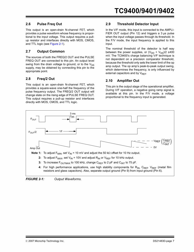
2.6 Pulse Freq OutThis output is an open-drain N-channel FET, whichprovides a pulse waveform whose frequency is propor-tional to the input voltage. This output requires a pull-up resistor and interfaces directly with MOS, CMOS,and TTL logic (see Figure 2-1).2.7 Output CommonThe sources of both the FREQ/2 OUT and the PULSEFREQ OUT are connected to this pin. An output levelswing from the drain voltage to ground, or to the VSSsupply, may be obtained by connecting this pin to theappropriate point.
2.8 Freq/2 OutThis output is an open-drain N-channel FET, whichprovides a square-wave one-half the frequency of thepulse frequency output. The FREQ/2 OUT output willchange state on the rising edge of PULSE FREQ OUT.This output requires a pull-up resistor and interfacesdirectly with MOS, CMOS, and TTL logic.
2.9 Threshold Detector InputIn the V/F mode, this input is connected to the AMPLI-FIER OUT output (Pin 12) and triggers a 3 µs pulsewhen the input voltage passes through its threshold. Inthe F/V mode, the input frequency is applied to thisinput.
The nominal threshold of the detector is half waybetween the power supplies, or (VDD + VSS)/2 ±400mV. The TC9400’s charge balancing V/F technique isnot dependent on a precision comparator threshold,because the threshold only sets the lower limit of the opamp output. The op amp’s peak-to-peak output swing,which determines the frequency, is only influenced byexternal capacitors and by VREF.
2.10 Amplifier OutThis pin is the output stage of the operational amplifier.During V/F operation, a negative going ramp signal isavailable at this pin. In the F/V mode, a voltageproportional to the frequency input is generated.
FIGURE 2-1: Output Waveforms.
3 ms Typ.
1/f
FOUT
FOUT/2
Amp Out
VREF
0V
CREFCINT
Note 1: To adjust FMIN, set VIN = 10 mV and adjust the 50 kΩ offset for 10 Hz output.
2: To adjust FMAX, set VIN = 10V and adjust RIN or VREF for 10 kHz output.
3: To increase FOUTMAX to 100 kHz, change CREF to 2 pF and CINT to 75 pF.
4: For high performance applications, use high stability components for RIN, CREF. VREF (metal filmresistors and glass capacitors). Also, separate output ground (Pin 9) from input ground (Pin 6).
© 2007 Microchip Technology Inc. DS21483D-page 7

TC9400/9401/9402
3.0 DETAILED DESCRIPTION
3.1 Voltage-to-Frequency (V/F) Circuit Description
The TC9400 V/F converter operates on the principal ofcharge balancing. The operation of the TC9400 iseasily understood by referring to Figure 3-1. The inputvoltage (VIN) is converted to a current (IIN) by the inputresistor. This current is then converted to a charge onthe integrating capacitor and shows up as a linearlydecreasing voltage at the output of the op amp. Thelower limit of the output swing is set by the thresholddetector, which causes the reference voltage to beapplied to the reference capacitor for a time period longenough to charge the capacitor to the reference volt-age. This action reduces the charge on the integratingcapacitor by a fixed amount (q = CREF x VREF), causingthe op amp output to step up a finite amount.
At the end of the charging period, CREF is shorted out.This dissipates the charge stored on the referencecapacitor, so that when the output again crosses zero,the system is ready to recycle. In this manner, the con-tinued discharging of the integrating capacitor by theinput is balanced out by fixed charges from the refer-
ence voltage. As the input voltage is increased, thenumber of reference pulses required to maintainbalance increases, which causes the output frequencyto also increase. Since each charge increment is fixed,the increase in frequency with voltage is linear. Inaddition, the accuracy of the output pulse width doesnot directly affect the linearity of the V/F. The pulsemust simply be long enough for full charge transfer totake place.
The TC9400 contains a “self-start” circuit to ensure theV/F converter always operates properly when power isfirst applied. In the event that, during power-on, the opamp output is below the threshold and CREF is alreadycharged, a positive voltage step will not occur. The opamp output will continue to decrease until it crosses the-3.0V threshold of the “self-start” comparator. Whenthis happens, an internal resistor is connected to the opamp input, which forces the output to go positive untilthe TC9400 is in its normal Operating mode.
The TC9400 utilizes low-power CMOS processing forlow input bias and offset currents, with very low powerdissipation. The open drain N-channel output FETsprovide high voltage and high current sink capability.
FIGURE 3-1: 10 Hz to 10 kHz V/F Converter.
–
+
+5V+5V
14VDD
+5V
RL10 kΩ
RL10 kΩ
8
10
9
FOUT
FOUT/2
11 3 msDelay
Self-Start
12
5
20 kΩ
60 pF
Op Amp
CINT820 pF CREF
180 pF 12 pFRIN
1 MΩVIN
+5V
-5V
50 kΩ510 kΩ
10 kΩ
3
1OffsetAdjust
IIN
Zero Adjust0V –10V
IBIAS VSS
4
-5V
2
OutputCommon
VREFOUT
RBIAS100 kΩ
AMP OUT
TC9400TC9401TC9402
GND6
ThresholdDetector
ThresholdDetect
Reference Voltage(Typically -5V)
÷2
VREF
7
-3V
INPUT
DS21483D-page 8 © 2007 Microchip Technology Inc.
TC9400/9401/9402
3.2 Voltage-to-Time MeasurementsThe TC9400 output can be measured in the timedomain as well as the frequency domain. Some micro-computers, for example, have extensive timing capabil-ity, but limited counter capability. Also, the responsetime of a time domain measurement is only the periodbetween two output pulses, while the frequencymeasurement must accumulate pulses during theentire counter time-base period.Time measurements can be made from either theTC9400’s PULSE FREQ OUT output, or from theFREQ/2 OUT output. The FREQ/2 OUT outputchanges state on the rising edge of PULSE FREQOUT, so FREQ/2 OUT is a symmetrical square wave atone-half the pulse output frequency. Timing measure-ments can, therefore, be made between successivePULSE FREQ OUT pulses, or while FREQ/2 OUT ishigh (or low).
© 2007 Microchip Technology Inc. DS21483D-page 9

TC9400/9401/9402
4.0 VOLTAGE-TO-FREQUENCY(V/F) CONVERTER DESIGN INFORMATION
4.1 Input/Output RelationshipsThe output frequency (FOUT) is related to the analoginput voltage (VIN) by the transfer equation:
EQUATION 4-1:
4.2 External Component Selection4.2.1 RIN
The value of this component is chosen to give a fullscale input current of approximately 10 µA:
EQUATION 4-2:
EQUATION 4-3:
Note that the value is an approximation and the exactrelationship is defined by the transfer equation. Inpractice, the value of RIN typically would be trimmed toobtain full scale frequency at VIN full scale (seeSection 4.3 “Adjustment Procedure”, AdjustmentProcedure). Metal film resistors with 1% tolerance orbetter are recommended for high accuracy applicationsbecause of their thermal stability and low noisegeneration.
4.2.2 CINTThe exact value is not critical but is related to CREF bythe relationship:
3CREF ≤ CINT ≤ 10CREF
Improved stability and linearity are obtained whenCINT ≤ 4CREF. Low leakage types are recommended,although mica and ceramic devices can be used inapplications where their temperature limits are notexceeded. Locate as close as possible to Pins 12and 13.
4.2.3 CREFThe exact value is not critical and may be used to trimthe full scale frequency (see Section 6.1 “Input/Out-put Relationships”, Input/Output Relationships).Glass film or air trimmer capacitors are recommendedbecause of their stability and low leakage. Locate asclose as possible to Pins 5 and 3 (see Figure 4-1).
FIGURE 4-1: Recommended CREF vs. VREF.
4.2.4 VDD, VSSPower supplies of ±5V are recommended. For highaccuracy requirements, 0.05% line and load regulationand 0.1 µF disc decoupling capacitors, located near thepins, are recommended.
4.3 Adjustment ProcedureFigure 3-1 shows a circuit for trimming the zerolocation. Full scale may be trimmed by adjusting RIN,VREF, or CREF. Recommended procedure for a 10 kHzfull scale frequency is as follows:
1. Set VIN to 10 mV and trim the zero adjust circuitto obtain a 10 Hz output frequency.
2. Set VIN to 10V and trim either RIN, VREF, or CREFto obtain a 10 kHz output frequency.
If adjustments are performed in this order, there shouldbe no interaction and they should not have to berepeated.
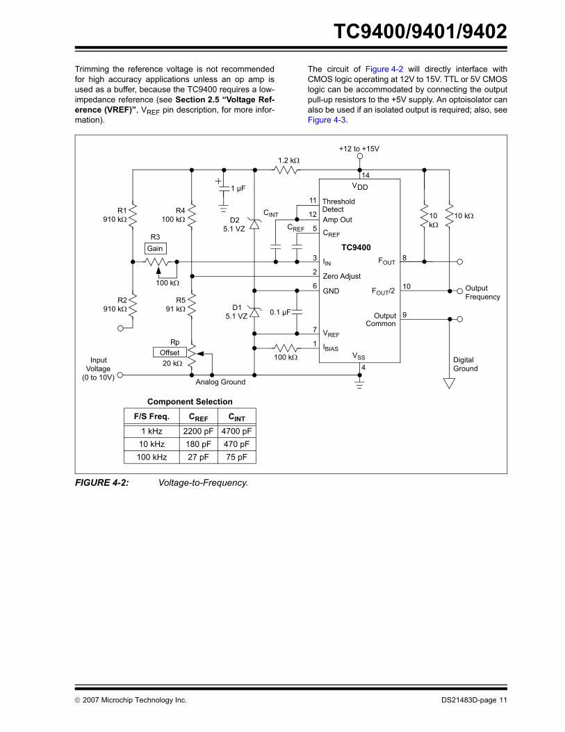
4.4 Improved Single Supply V/F Converter Operation
A TC9400, which operates from a single 12 to 15Vvariable power source, is shown in Figure 4-2. Thiscircuit uses two Zener diodes to set stable biasinglevels for the TC9400. The Zener diodes also providethe reference voltage, so the output impedance andtemperature coefficient of the Zeners will directly affectpower supply rejection and temperature performance.Full scale adjustment is accomplished by trimming theinput current.
Frequency OutVINRIN-------- 1
VREF( ) CREF( )------------------------------------•=
VIN FULL SCALE
10 μARIN ≅
10V10 μA
RIN ≅ = 1 MΩ
500
400
300
200
100
0 -1 -2 -3 -4 -5 -6 -7VREF (V)
C REF
(pF)
+12
pF
10 kHz
100 kHz
VDD = +5VVSS = -5VRIN = 1MWVIN = +10VTA = +25°C
DS21483D-page 10 © 2007 Microchip Technology Inc.
TC9400/9401/9402
Trimming the reference voltage is not recommendedfor high accuracy applications unless an op amp isused as a buffer, because the TC9400 requires a low-impedance reference (see Section 2.5 “Voltage Ref-erence (VREF)”, VREF pin description, for more infor-mation).The circuit of Figure 4-2 will directly interface withCMOS logic operating at 12V to 15V. TTL or 5V CMOSlogic can be accommodated by connecting the outputpull-up resistors to the +5V supply. An optoisolator canalso be used if an isolated output is required; also, seeFigure 4-3.
FIGURE 4-2: Voltage-to-Frequency.
R1910 kΩ
R4
1 µF
D25.1 VZ
R2910 kΩ
R591 kΩ
RpOffset20 kΩ
100 kΩ
D15.1 VZ 0.1 µF
100 kΩ
CREF
CINT
1.2 kΩ
+12 to +15V
10 10 kΩ
OutputFrequency
DigitalGround
Analog Ground
InputVoltage
(0 to 10V)
R3Gain TC9400
11
12
5
3
2
6
7
1
4
14
9
10
8
ThresholdDetectAmp Out
CREF
IIN
Zero Adjust
GND
VREF
IBIAS
OutputCommon
FOUT/2
FOUT
VDD
VSS
100 kΩkΩ
Component Selection
F/S Freq. CREF CINT
1 kHz 2200 pF 4700 pF10 kHz 180 pF 470 pF
100 kHz 27 pF 75 pF
© 2007 Microchip Technology Inc. DS21483D-page 11
TC9400/9401/9402
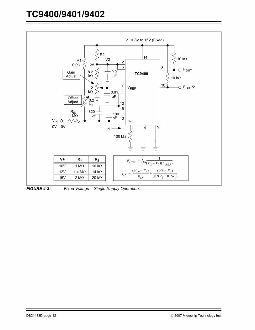
FIGURE 4-3: Fixed Voltage – Single Supply Operation.
V+ = 8V to 15V (Fixed)
14
8
10 kΩ
10 kΩ
FOUT
FOUT/210
1 4 9
100 kΩ
0V–10V IIN
180 pF
820 pF
3
512
117
0.01µF
2kΩ
8.2kΩ
62
V2R2
0.9Ω R1
0.2R1
RIN1 MΩ
IIN
VREF
TC9400
OffsetAdjust
GainAdjust
5V
0.01µF
VIN
V+ R1 R2
10V 1 MΩ 10 kΩ
12V 1.4 MΩ 14 kΩ
15V 2 MΩ 20 kΩ
FOUT IIN1
V2 V7–( ) CREF( )------------------------------------------=
IINVIN V2–( )
RIN--------------------------
V+ V2–( )0.9R1 0.2R1+( )---------------------------------------+=
DS21483D-page 12 © 2007 Microchip Technology Inc.

TC9400/9401/9402
5.0 FREQUENCY-TO-VOLTAGE (F/V) CIRCUIT DESCRIPTION
When used as an F/V converter, the TC9400 generatesan output voltage linearly proportional to the inputfrequency waveform.
Each zero crossing at the threshold detector’s inputcauses a precise amount of charge (q = CREF x VREF)to be dispensed into the op amp’s summing junction.This charge, in turn, flows through the feedbackresistor, generating voltage pulses at the output of theop amp. A capacitor (CINT) across RINT averages thesepulses into a DC voltage, which is linearly proportionalto the input frequency.
© 2007 Microchip Technology Inc. DS21483D-page 13

TC9400/9401/9402
6.0 F/V CONVERTER DESIGN INFORMATION
6.1 Input/Output RelationshipsThe output voltage is related to the input frequency(FIN) by the transfer equation:
EQUATION 6-1:
The response time to a change in FIN is equal to (RINTCINT). The amount of ripple on VOUT is inverselyproportional to CINT and the input frequency.
CINT can be increased to lower the ripple. Values of1 µF to 100 µF are perfectly acceptable for low frequen-cies.
When the TC9400 is used in the Single Supply mode,VREF is defined as the voltage difference between Pin 7and Pin 2.
6.2 Input Voltage LevelsThe input frequency is applied to the ThresholdDetector input (Pin 11). As discussed in the V/F circuitsection of this data sheet, the threshold of Pin 11 isapproximately (VDD + VSS)/2 ±400 mV. Pin 11’s inputvoltage range extends from VDD to about 2.5V belowthe threshold. If the voltage on Pin 11 goes more than2.5 volts below the threshold, the V/F mode start-upcomparator will turn on and corrupt the output voltage.The Threshold Detector input has about 200 mV ofhysteresis.
In ±5V applications, the input voltage levels for theTC9400 are ±400 mV, minimum. If the frequencysource being measured is unipolar, such as TTL orCMOS operating from a +5V source, then an ACcoupled level shifter should be used. One such circuitis shown in Figure 6-1(a).
The level shifter circuit in Figure 6-1(b) can be used insingle supply F/V applications. The resistor dividerensures that the input threshold will track the supplyvoltages. The diode clamp prevents the input fromgoing far enough in the negative direction to turn on thestart-up comparator. The diode’s forward voltagedecreases by 2.1 mV/°C, so for high ambienttemperature operation, two diodes in series arerecommended.
FIGURE 6-1: Frequency Input Level Shifter.
VOUT = [VREF CREF RINT] FIN
+5V
14
6 4
+5V
-5V
VDD
1.0
1133 kΩ
IN914
VSS
DET
TC9400
(a) ±5V Supply (b) Single Supply
0.01 µFFrequency
Input
0V
GND
+8V to +15V
14
10 kΩ
4
+5V
VDD
1.0
1133 kΩ
IN914
VSS
DET
TC9400
0.01 µF Frequency
Input
0V
0.1 µF 10 kΩ
MΩ MΩ
DS21483D-page 14 © 2007 Microchip Technology Inc.

TC9400/9401/9402
FIGURE 6-2: F/V Single Supply F/V Converter.
6.3 Input BufferFOUT and FOUT/2 are not used in the F/V mode. How-ever, these outputs may be useful for some applica-tions, such as a buffer to feed additional circuitry. Then,FOUT will follow the input frequency waveform, exceptthat FOUT will go high 3 µs after FIN goes high; FOUT/2will be square wave with a frequency of one-half FOUT.
If these outputs are not used, Pins 8, 9 and 10 should beconnected to ground (see Figure 6-3 and Figure 6-4).
FIGURE 6-3: F/V Digital Outputs.
Offset Adjust
10 kΩ
.01 µF6.2V
IN914
33 kΩ
100 kΩ
500 kΩ
0.1 µF
100 kΩ
V+ = 10V to 15V
1
47 pF
VOUTFrequencyInput
TC9400
6
10 kΩ
2
11
1.04
14
12
3
5
GND
VREFOUT
IIN
ZeroAdjust
VREFIBIAS
Amp Out
VDD
VSS
GND6
7
1.0 kΩ
V+
1.0 kΩ
0.01 µF
.001 µF
DET
Note: The output is referenced to Pin 6, which is at 6.2V (Vz). For frequency meter applications,a 1 mA meter with a series scaling resistor can be placed across Pins 6 and 12.
MΩ
MΩ
0.5 ms Min
5.0 msMin
Delay = 3 ms
Input
FOUT
FOUT/2
© 2007 Microchip Technology Inc. DS21483D-page 15
TC9400/9401/9402
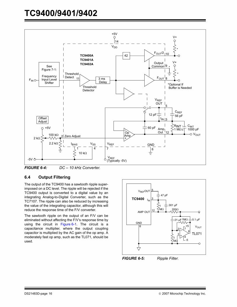
FIGURE 6-4: DC – 10 kHz Converter.
6.4 Output FilteringThe output of the TC9400 has a sawtooth ripple super-imposed on a DC level. The ripple will be rejected if theTC9400 output is converted to a digital value by anintegrating Analog-to-Digital Converter, such as theTC7107. The ripple can also be reduced by increasingthe value of the integrating capacitor, although this willreduce the response time of the F/V converter.
The sawtooth ripple on the output of an F/V can beeliminated without affecting the F/V’s response time byusing the circuit in Figure 6-1. The circuit is acapacitance multiplier, where the output couplingcapacitor is multiplied by the AC gain of the op amp. Amoderately fast op amp, such as the TL071, should beused.
FIGURE 6-5: Ripple Filter.
TC9400ATC9401ATC9402A
+5V
14VDD
V+
V+
FOUT/2
FOUT
Output Common
10
9
8
5
3
12
12 pFCREF56 pF
CINT1000 pF
RINT1 MΩ60 pF Amp
Out VOUT
VSSIBIAS1 4
10 kΩ
2.2 kΩ
100 kΩ2 kΩ
-5V
+5V
Zero Adjust2
7
(Typically -5V)
VREF
FIN11
ThresholdDetector
3 msDelay
*
*
*
*Optional If Buffer is Needed
OffsetAdjust
VREF OUT
IIN
42
–
+
Op Amp
+
VREF
SeeFigure 7-1:
FrequencyInput Level
Shifter
6GND
ThresholdDetect
1
47 pF
VOUT
TC9400
12
3
5VREFOUT
IIN
GND
AMP OUT
6
.001 µF
+
–
13
2
.01 µF 1MΩ 0.1 µF
+57
6
4-5
TL071
200ΩMΩ
MΩ
DS21483D-page 16 © 2007 Microchip Technology Inc.

TC9400/9401/9402
7.0 F/V POWER-ON RESETIn F/V mode, the TC9400 output voltage will occasion-ally be at its maximum value when power is firstapplied. This condition remains until the first pulse isapplied to FIN. In most frequency measurementapplications, this is not a problem because properoperation begins as soon as the frequency input isapplied.
In some cases, however, the TC9400 output must bezero at power-on without a frequency input. In suchcases, a capacitor connected from Pin 11 to VDD willusually be sufficient to pulse the TC9400 and provide aPower-on Reset (see Figure 7-1 (a) and (b)). Wherepredictable power-on operation is critical, a morecomplicated circuit, such as Figure 7-1 (b), may berequired.
FIGURE 7-1: Power-On Operation/Reset.
VDD
14
11
1000 pF
ThresholdDetector
1 kΩFIN
VDD
100 kΩ
1 µF
3
4
8
6
FIN
12516VCC B R C
Q
VSSA
CLRACD4538
TC9400
(a) (b)
To TC9400
© 2007 Microchip Technology Inc. DS21483D-page 17

TC9400/9401/9402
8.0 PACKAGE INFORMATION
8.1 Package Marking Information
Legend: XX...X Customer-specific informationY Year code (last digit of calendar year)YY Year code (last 2 digits of calendar year)WW Week code (week of January 1 is week ‘01’)NNN Alphanumeric traceability code Pb-free JEDEC designator for Matte Tin (Sn)* This package is Pb-free. The Pb-free JEDEC designator ( )
can be found on the outer packaging for this package.
Note: In the event the full Microchip part number cannot be marked on one line, it willbe carried over to the next line, thus limiting the number of availablecharacters for customer-specific information.
3e
3e
XXXXXXXXXXXXXXYYWWNNN
14-Lead CERDIP
XXXXXXXXXXXXXX
0731256
Example: (Front View)
TC9400EJD
14-Lead PDIP
XXXXXXXXXXXXXXXXXXXXXXXXXXXX
YYWWNNN
Example: (Front View)
14-Lead SOIC (.150”)
XXXXXXXXXXXXXXXXXXXXXX
YYWWNNN
Example: (Front View)
Y2026
Example: (Back View)
Y2026
Example: (Back View)
TC9400CPD ^^
07312563e
TC9400EOD ^^
0731256
Example: (Back View)
3e
Y2026
DS21483D-page 18 © 2007 Microchip Technology Inc.

TC9400/9401/9402
14-Lead Ceramic Dual In-Line (JD) – .300" Body [CERDIP]
Notes:1. Pin 1 visual index feature may vary, but must be located within the hatched area.2. § Significant Characteristic.3. Dimensioning and tolerancing per ASME Y14.5M.
BSC: Basic Dimension. Theoretically exact value shown without tolerances.
Note: For the most current package drawings, please see the Microchip Packaging Specification located at http://www.microchip.com/packaging
Units INCHES
Dimension Limits MIN NOM MAX
Number of Pins N 14
Pitch e .100 BSC
Top to Seating Plane A – – .200
Standoff § A1 .015 – –
Ceramic Package Height A2 .140 – .175
Shoulder to Shoulder Width E .290 – .325
Ceramic Package Width E1 .230 .288 .300
Overall Length D .740 .760 .780
Tip to Seating Plane L .125 – .200
Lead Thickness c .008 – .015
Upper Lead Width b1 .045 – .065
Lower Lead Width b .015 – .023
Overall Row Spacing E2 .320 – .410
N
E1
D
1 2
NOTE 1
A
A1
b1
b e
L
A2
E
c
E2
Microchip Technology Drawing C04-002B
© 2007 Microchip Technology Inc. DS21483D-page 19

TC9400/9401/9402
14-Lead Plastic Dual In-Line (PD) – 300 mil Body [PDIP]
Notes:1. Pin 1 visual index feature may vary, but must be located with the hatched area.2. § Significant Characteristic.3. Dimensions D and E1 do not include mold flash or protrusions. Mold flash or protrusions shall not exceed .010" per side.4. Dimensioning and tolerancing per ASME Y14.5M.
BSC: Basic Dimension. Theoretically exact value shown without tolerances.
Note: For the most current package drawings, please see the Microchip Packaging Specification located at http://www.microchip.com/packaging
Units INCHES
Dimension Limits MIN NOM MAX
Number of Pins N 14
Pitch e .100 BSC
Top to Seating Plane A – – .210
Molded Package Thickness A2 .115 .130 .195
Base to Seating Plane A1 .015 – –
Shoulder to Shoulder Width E .290 .310 .325
Molded Package Width E1 .240 .250 .280
Overall Length D .735 .750 .775
Tip to Seating Plane L .115 .130 .150
Lead Thickness c .008 .010 .015
Upper Lead Width b1 .045 .060 .070
Lower Lead Width b .014 .018 .022
Overall Row Spacing § eB – – .430
N
E1
D
NOTE 1
1 2 3
E
c
eB
A2
L
A
A1b1
b e
Microchip Technology Drawing C04-005B
DS21483D-page 20 © 2007 Microchip Technology Inc.
TC9400/9401/9402
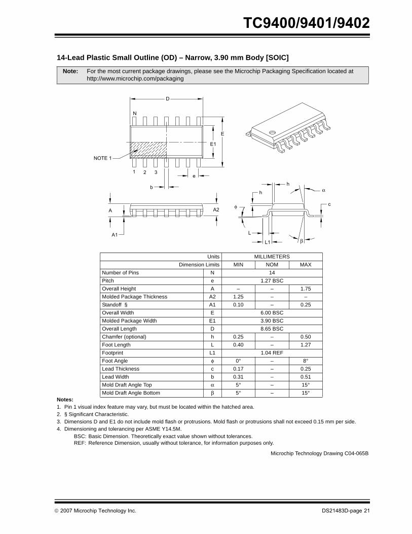
14-Lead Plastic Small Outline (OD) – Narrow, 3.90 mm Body [SOIC]
Notes:1. Pin 1 visual index feature may vary, but must be located within the hatched area.2. § Significant Characteristic.3. Dimensions D and E1 do not include mold flash or protrusions. Mold flash or protrusions shall not exceed 0.15 mm per side.4. Dimensioning and tolerancing per ASME Y14.5M.
BSC: Basic Dimension. Theoretically exact value shown without tolerances.REF: Reference Dimension, usually without tolerance, for information purposes only.
Note: For the most current package drawings, please see the Microchip Packaging Specification located at http://www.microchip.com/packaging
Units MILLIMETERS
Dimension Limits MIN NOM MAX
Number of Pins N 14
Pitch e 1.27 BSC
Overall Height A – – 1.75
Molded Package Thickness A2 1.25 – –
Standoff § A1 0.10 – 0.25
Overall Width E 6.00 BSC
Molded Package Width E1 3.90 BSC
Overall Length D 8.65 BSC
Chamfer (optional) h 0.25 – 0.50
Foot Length L 0.40 – 1.27
Footprint L1 1.04 REF
Foot Angle φ 0° – 8°
Lead Thickness c 0.17 – 0.25
Lead Width b 0.31 – 0.51
Mold Draft Angle Top α 5° – 15°
Mold Draft Angle Bottom β 5° – 15°
NOTE 1
N
D
E
E1
1 2 3
b
e
A
A1
A2
L
L1
c
h
hα
β
φ
Microchip Technology Drawing C04-065B
© 2007 Microchip Technology Inc. DS21483D-page 21

TC9400/9401/9402
NOTES:DS21483D-page 22 © 2007 Microchip Technology Inc.
TC9400/9401/9402
APPENDIX A: REVISION HISTORY
Revision D (September 2007)The following is the list of modifications:
1. Corrected Figure 6-1.2. Added History section.3. Updated package marking information and
package outline drawings4. Added Product identification System section.
Revision C (May 2006)
Revision B (May 2002)
Revision A (April 2002)• Original Release of this Document.
© 2007 Microchip Technology Inc. DS21483D-page 23

TC9400/9401/9402
NOTES:DS21483D-page 24 © 2007 Microchip Technology Inc.

TC9400/9401/9402
PRODUCT IDENTIFICATION SYSTEMTo order or obtain information, e.g., on pricing or delivery, refer to the factory or the listed sales office.
PART NO. X /XX
PackageTemperatureRange
Device
Device TC9400: Voltage-to-Frequency Converter
TC9401: Voltage-to-Frequency ConverterTC9402: Voltage-to-Frequency Converter
Temperature Range E = -40°C to +85°C (Extended)C = 0°C to +70°C (Commercial)
Package JD = Ceramic Dual-Inline (.300” Body), 14-leadPD = Plastic Dual-Inline (300 mil Body), 14-leadOD = Plastic Small Outline (3.90 MM Body), 14-leadOD713 = Plastic Small Outline (3.90 MM Body), 14-lead
Tape and Reel.
Examples:a) TC9400COD: 0°C to +70°C,
14LD SOIC package.b) TC9400COD713:0°C to +70°C,
14LD SOIC package,Tape and Reel
c) TC9400CPD: 0°C to +70°C,14LD PDIP package.
d) TC9400EJD: -40°C to +85°C,14LD PDIP package.
a) TC9401CPD: 0°C to +70°C,14LD PDIP package.
b) TC9401EJD: -40°C to +85°C,14LD CERDIP package.
a) TC9402CPD: 0°C to +70°C,14LD PDIP package.
b) TC9402EJD: -40°C to +85°C,14LD CERDIP package.
© 2007 Microchip Technology Inc. DS21483D-page 25

TC9400/9401/9402
NOTES:DS21483D-page 26 © 2007 Microchip Technology Inc.

Note the following details of the code protection feature on Microchip devices:• Microchip products meet the specification contained in their particular Microchip Data Sheet.
• Microchip believes that its family of products is one of the most secure families of its kind on the market today, when used in the intended manner and under normal conditions.
• There are dishonest and possibly illegal methods used to breach the code protection feature. All of these methods, to our knowledge, require using the Microchip products in a manner outside the operating specifications contained in Microchip’s Data Sheets. Most likely, the person doing so is engaged in theft of intellectual property.
• Microchip is willing to work with the customer who is concerned about the integrity of their code.
• Neither Microchip nor any other semiconductor manufacturer can guarantee the security of their code. Code protection does not mean that we are guaranteeing the product as “unbreakable.”
Code protection is constantly evolving. We at Microchip are committed to continuously improving the code protection features of ourproducts. Attempts to break Microchip’s code protection feature may be a violation of the Digital Millennium Copyright Act. If such actsallow unauthorized access to your software or other copyrighted work, you may have a right to sue for relief under that Act.
Information contained in this publication regarding deviceapplications and the like is provided only for your convenienceand may be superseded by updates. It is your responsibility toensure that your application meets with your specifications.MICROCHIP MAKES NO REPRESENTATIONS ORWARRANTIES OF ANY KIND WHETHER EXPRESS ORIMPLIED, WRITTEN OR ORAL, STATUTORY OROTHERWISE, RELATED TO THE INFORMATION,INCLUDING BUT NOT LIMITED TO ITS CONDITION,QUALITY, PERFORMANCE, MERCHANTABILITY ORFITNESS FOR PURPOSE. Microchip disclaims all liabilityarising from this information and its use. Use of Microchipdevices in life support and/or safety applications is entirely atthe buyer’s risk, and the buyer agrees to defend, indemnify andhold harmless Microchip from any and all damages, claims,suits, or expenses resulting from such use. No licenses areconveyed, implicitly or otherwise, under any Microchipintellectual property rights.
© 2007 Microchip Technology Inc.
Trademarks
The Microchip name and logo, the Microchip logo, Accuron, dsPIC, KEELOQ, KEELOQ logo, microID, MPLAB, PIC, PICmicro, PICSTART, PRO MATE, rfPIC and SmartShunt are registered trademarks of Microchip Technology Incorporated in the U.S.A. and other countries.
AmpLab, FilterLab, Linear Active Thermistor, Migratable Memory, MXDEV, MXLAB, SEEVAL, SmartSensor and The Embedded Control Solutions Company are registered trademarks of Microchip Technology Incorporated in the U.S.A.
Analog-for-the-Digital Age, Application Maestro, CodeGuard, dsPICDEM, dsPICDEM.net, dsPICworks, dsSPEAK, ECAN, ECONOMONITOR, FanSense, FlexROM, fuzzyLAB, In-Circuit Serial Programming, ICSP, ICEPIC, Mindi, MiWi, MPASM, MPLAB Certified logo, MPLIB, MPLINK, PICkit, PICDEM, PICDEM.net, PICLAB, PICtail, PowerCal, PowerInfo, PowerMate, PowerTool, REAL ICE, rfLAB, Select Mode, Smart Serial, SmartTel, Total Endurance, UNI/O, WiperLock and ZENA are trademarks of Microchip Technology Incorporated in the U.S.A. and other countries.
SQTP is a service mark of Microchip Technology Incorporated in the U.S.A.
All other trademarks mentioned herein are property of their respective companies.
© 2007, Microchip Technology Incorporated, Printed in the U.S.A., All Rights Reserved.
Printed on recycled paper.
DS21483D-page 27
Microchip received ISO/TS-16949:2002 certification for its worldwide headquarters, design and wafer fabrication facilities in Chandler and Tempe, Arizona; Gresham, Oregon and design centers in California and India. The Company’s quality system processes and procedures are for its PIC® MCUs and dsPIC® DSCs, KEELOQ® code hopping devices, Serial EEPROMs, microperipherals, nonvolatile memory and analog products. In addition, Microchip’s quality system for the design and manufacture of development systems is ISO 9001:2000 certified.

DS21483D-page 28 © 2007 Microchip Technology Inc.
AMERICASCorporate Office2355 West Chandler Blvd.Chandler, AZ 85224-6199Tel: 480-792-7200 Fax: 480-792-7277Technical Support: http://support.microchip.comWeb Address: www.microchip.comAtlantaDuluth, GA Tel: 678-957-9614 Fax: 678-957-1455BostonWestborough, MA Tel: 774-760-0087 Fax: 774-760-0088ChicagoItasca, IL Tel: 630-285-0071 Fax: 630-285-0075DallasAddison, TX Tel: 972-818-7423 Fax: 972-818-2924DetroitFarmington Hills, MI Tel: 248-538-2250Fax: 248-538-2260KokomoKokomo, IN Tel: 765-864-8360Fax: 765-864-8387Los AngelesMission Viejo, CA Tel: 949-462-9523 Fax: 949-462-9608Santa ClaraSanta Clara, CA Tel: 408-961-6444Fax: 408-961-6445TorontoMississauga, Ontario, CanadaTel: 905-673-0699 Fax: 905-673-6509
ASIA/PACIFICAsia Pacific OfficeSuites 3707-14, 37th FloorTower 6, The GatewayHarbour City, KowloonHong KongTel: 852-2401-1200Fax: 852-2401-3431Australia - SydneyTel: 61-2-9868-6733Fax: 61-2-9868-6755China - BeijingTel: 86-10-8528-2100 Fax: 86-10-8528-2104China - ChengduTel: 86-28-8665-5511Fax: 86-28-8665-7889China - FuzhouTel: 86-591-8750-3506 Fax: 86-591-8750-3521China - Hong Kong SARTel: 852-2401-1200 Fax: 852-2401-3431China - QingdaoTel: 86-532-8502-7355Fax: 86-532-8502-7205China - ShanghaiTel: 86-21-5407-5533 Fax: 86-21-5407-5066China - ShenyangTel: 86-24-2334-2829Fax: 86-24-2334-2393China - ShenzhenTel: 86-755-8203-2660 Fax: 86-755-8203-1760China - ShundeTel: 86-757-2839-5507 Fax: 86-757-2839-5571China - WuhanTel: 86-27-5980-5300Fax: 86-27-5980-5118China - XianTel: 86-29-8833-7252Fax: 86-29-8833-7256
ASIA/PACIFICIndia - BangaloreTel: 91-80-4182-8400 Fax: 91-80-4182-8422India - New DelhiTel: 91-11-4160-8631Fax: 91-11-4160-8632India - PuneTel: 91-20-2566-1512Fax: 91-20-2566-1513Japan - YokohamaTel: 81-45-471- 6166 Fax: 81-45-471-6122Korea - DaeguTel: 82-53-744-4301Fax: 82-53-744-4302Korea - SeoulTel: 82-2-554-7200Fax: 82-2-558-5932 or 82-2-558-5934Malaysia - PenangTel: 60-4-646-8870Fax: 60-4-646-5086Philippines - ManilaTel: 63-2-634-9065Fax: 63-2-634-9069SingaporeTel: 65-6334-8870Fax: 65-6334-8850Taiwan - Hsin ChuTel: 886-3-572-9526Fax: 886-3-572-6459Taiwan - KaohsiungTel: 886-7-536-4818Fax: 886-7-536-4803Taiwan - TaipeiTel: 886-2-2500-6610 Fax: 886-2-2508-0102Thailand - BangkokTel: 66-2-694-1351Fax: 66-2-694-1350
EUROPEAustria - WelsTel: 43-7242-2244-39Fax: 43-7242-2244-393Denmark - CopenhagenTel: 45-4450-2828 Fax: 45-4485-2829France - ParisTel: 33-1-69-53-63-20 Fax: 33-1-69-30-90-79Germany - MunichTel: 49-89-627-144-0 Fax: 49-89-627-144-44Italy - Milan Tel: 39-0331-742611 Fax: 39-0331-466781Netherlands - DrunenTel: 31-416-690399 Fax: 31-416-690340Spain - MadridTel: 34-91-708-08-90Fax: 34-91-708-08-91UK - WokinghamTel: 44-118-921-5869Fax: 44-118-921-5820
WORLDWIDE SALES AND SERVICE
06/25/07