technical university of koŠice
TRANSCRIPT

TECHNICAL UNIVERSITY OF KOŠICE
FACULTY OF ELECTRICAL ENGINEERING AND INFORMATICS
DEPARTMENT OF TECHNOLOGIES IN ELECTRONICS
Manufacturing Processes in Electronics
Applied Informatics

Electronics Assembling Technology
1. Introduction: The electronics assembly process flow
The rapid development of microelectronics devices and their assembling technologies is
accompanied by the dramatic change of the knowledge required from all technical personnel
(engineers, technicians, skilled or even unskilled workers) employed in this field. It causes a
contradiction of the high population of unemployment people with the increasing number of
working places offered by the electronics assembling companies, in particular in the East
parts of the European Union, as such companies move from the West to these regions in the
expectation of low salary rates.
Chapters 1. Introduction: The electronics assembly process flow,
2. Printed wiring boards,
3. Surface finishes used on printed wiring boards
4. Solder Paste stencil printing
5. Component placement
6. Reflow soldering, reflow ovens and temperature profiling
7. Wave soldering and thermal profiles
This introduction provides an overview of the electronics assembly process flow,
including three main parts, namely the Components and Printed Circuits Boards, the
Assembling Technologies, and the Inspection, Test and Quality Management chapters.
There are two primary categories of electronic components: through-hole and surface
mount. Through-hole components have leads that are long and thick enough to be inserted
through the holes in the printed circuit board. Surface mount components have much smaller
leads or terminations that attach directly onto the lands on the surface of the board.
The overall assembly process includes incoming inspection and preparation of circuit
boards and components; automatic component insertion and placement; manual insertion of
components; wave and reflow soldering; hand soldering; assembly cleaning; electrical test;
rework and repair; conformal coating and final system assembly.
The different combinations of electronics assemblies usually require the application of
the combination of the different processes, as well.

Electronics Assembly is the process of attaching component leads or terminations to lands or pads of conductors on a circuit board and then join them by soldering.
There are two primary categories of components and assemblies; through hole and surface mount.
Electronics assembly variations –
Through-Hole Technology (THT)
At through-hole technology (THT), component leads are inserted through holes in the printed wiring board (PWB); and soldered to the lands on its other side.
A TH component is the DIL IC (dual-in-line integrated circuit), whose leads usually have a pitch of 2,54 mm (0,1”)
Through-hole assembly basically consists of component insertion and soldering.
Through-hole components, such as ICs, often come in dual-in-line packages, or DIPs.
They usually arrive from the supplier in antistatic plastic tubes. Other active components such
as transistors are packaged in bags or boxes and may require lead forming and manual
insertion.
Small axial-lead components, such as resistors, capacitors and diodes, are usually
packaged on tape and reel for automatic sequencing, lead forming and insertion.
SMT – Surface Mounting Technology
Process steps:
1. Solder paste application
2. Adhesive application for wave soldering
3. Components placement
4. Adhesive curing by heat or UV light
5. Reflow or Wave Soldering
6. Board cleaning
Terminations of surface mount devices (SMDs) are attached to the board pads by soldering to make both electrical and mechanical connections.
In some cases conductive adhesive joints are used.
Surface mount technology is more advanced than through-hole technology. Rather
than being inserted through holes in the circuit board, surface mount component leads sit on
lands on the surface of the board.
Surface mount assembly consists of three basic processes:
• solder paste application,
• component placement and
• reflow soldering.

Electronics assembly combinations
The different combinations of electronics assemblies usually require the application of the
combination of the through hole and the surface mount assembling processes as well as the
use of one side or both sides of the printed circuit boards. An example of this complex
approach is the use of automatic insertion of surface mount components and manual insertion
of the through-hole ones, followed by reflow and selective wave soldering of the same
assembly.
The assembly line for reflow soldering
According to the usual process flow a surface mount assembling line consists of three main
types of equipment: a stencil printer for the application of solder paste onto the pads of the
printed circuit boards; placement machine(s) for picking up the components and placing them
on the boards; and a reflow oven to melt the solder paste and make the solder joints. In most
cases inspection systems are also included after each main process steps into the complete
assembly line, where conveyors and handling tools move the boards from one machine to the
others throughout the whole line.

Types of discrete components by function and assembling
Active components: amplify the electric signal, need energy source,built from semiconductor materials
Passive components: amplify the electric signal, do not need energy source, built on insulating materials
Assembling types of components:
Through Hole components
Electronics assembly is the process of placing components onto a printed circuit board
and attaching the leads or terminations of the components to the lands or pads of conductors
on the board and then joins them by soldering.
There are different aspects to categorize discrete components, e.g. according to their
function, materials, size, form of termination, type of packaging, suitability for assembling,
etc.
According to its function a component is either active or passive. Active components
can amplify and modify the input electric parameter, like voltage or current, by using some
supplying power. On the other hand, passive components can only modify the electric
parameters, and do not need any supplying power. Typical examples for active components
are transistors and most ICs, while for passive components there are the resistors and
capacitors.
On the basis of the assembling method, for which the discrete component is suitable,
the classification can be through-hole (TH), surface-mount (SM) and chip components.
Through-hole components have wire or strip leads, which are suitable for inserting through
the holes of a PWB and fixing by soldering. The fix-terminated dual-inline package (DIP or
DIL package) is a characteristic example for TH components.
Surface-mount components (SMCs) have no or have only very small leads, so they are
unsuitable for through-hole assembly. Furthermore, SMCs are usually much smaller than the
through-hole ones.
Chips are leadless functional elements, and generally require special assembling
processes, like eutectic die bonding and thermo-compression wire bonding. Passive chip
components like chip resistors and chip capacitors, however, can be assembled by surface
mounting, while for active components the chip-scale (or chip-size) packaged chips are in use.

Surface Mount passive components and integrated circuits
Multilayer ceramic capacitor PLCC:Plastic Leaded Chip Carrier
QFP:Quad Flat Pack
Thick film chip resistor SOIC:Small Outline Integrated Circuit
A surface-mount component is a leaded or leadless electronic component that is
capable of being attached to a circuit board or a substrate by surface mounting, i.e. without
through hole insertion, and, as a consequence, its terminals are soldered directly onto
soldering pads, i.e. lands of the conductive pattern of the board or the substrate. When a
surface-mount component is leaded, its leads are very small, thus not suitable for through-hole
insertion, alike a leadless component which has external connections consisting of metalized
terminations that are integral part of the component body. The leads usually have the
characteristic shape of gull's wing, that is, the leads extend horizontally from the component
body centreline, but they are bent 90 degrees downward immediately past the body and bent
again 90 degrees outward just bellow the bottom of the body.
The most popular passive components are the SM (or chip) resistors and capacitors.
The active surface-mount components appear either in the small outline (SO) or in the chip
carrier (CC) packaging types. For higher lead counts the flat packs are in use, in particular
quad flat packs (QFPs), which are similar to SOICs, but they have finer pitches and with leads
on all four sides of the package.
Surface Mount ICs with high lead count
QFP (Quad Flat Pack)
Very high number of leads(up to 1000) are locatedat all the four sides of thepackagePitch minimum is 0,3 mm
FC–PBGA (Flip Chip – Plastic Ball Grid Array

The most modern alternatives of QFPs are ball grid arrays (BGAs), which are packages with
solder ball terminations throughout the area on the bottom of the package, similarly to a chip
size package and a flip-chip. In the course of assembling, these ball terminations are soldered
to an array of pads on the circuit board. BGAs have inherently high input/output count
capabilities for a given size package, show robustness for assembling processes, so they can
be excellently used for packaging of circuits modules.
Substrates: Types of Printed Wiring Boards
In an electronic assembly the substrate or circuit board supports the components mechanically, and interconnects their terminations electrically. Printed wiring board is the general term for completely processed printed wiring configurations, including single-sided, double-sided and multilayer boards with rigid, flexible and rigid-flex base materials.For circuit cards and modules the rigid printed wiring boards are used, while flexible and rigid-flex printed wirings are popular for the interconnection of cards placed in different position in equipment or of different units.
Flexible printed wiring boardRigid printed wiring board
In any electronic assembly there is a special component, the substrate or circuit
board which purpose is
- to support and fix mechanically the other components,
- to interconnect the proper terminations of the components, and
- to assist in the dissipation of heat generated by the components (including the substrate
itself).
The substrate is made up of an insulating base material, with conductive pattern upon and/or
in it for the interconnections. In some cases the substrate also contains integrated passive
elements formed from other structured layers.
The main aspects and groups for selecting and categorising PWBs are as follows:
- rigidity of the insulating board: rigid, flexible, or combined (rigid-flex);
- number of conductive layers: single-sided, double-sided, or multilayer;
- type of holes: nonmetallized holes, plated-through holes, or vias, including through-board,
blind, and buried vias;
- quality of the conductive pattern: rough, fine, or very fine;
- type of the connector: indirect, edge-board, or none; etc.

Printed Wiring Boards
Printed wiring board (PWB) is a substrate, which is made up of an insulating board with copper foil tracks on it. The components are fixed to the PWB and connected to the conductive copper tracks by soldering. In general, the base material of a PWB is a copper clad laminate, and the conductive pattern is prepared from the copper foil by subtractive technology, that is by the combination of photolithography and chemical etching. Multilayer boards are made by the lamination of single boards and adhesive layers. The patterns of the different layers are connected with plated holes (or vias).
In accordance with the everyday usage, a printed wiring board (PWB) is a substrate,
which is made up of an insulating board with copper foil tracks on its outer surfaces
(sometimes only on one of the outer surfaces, more often in the form of inner layers as well).
The components are fixed to the PWB and connected to the conductive copper tracks by
soldering. Sometimes in the technical slang the board is named printed circuit board (PCB)
and the assembly is named printed circuit (PC), but these names are slightly incorrect.
Assembling process steps defined by soldering

It is usually the applied soldering process that determines the whole process sequence.
The reason is that when wave soldering is used as the final step in surface mounting, the
board should be turned over to touch the solder wave, and consequently, all components
should be adhered previously to the board to avoid components falling down.
On the other hand, when reflow soldering is applied, the use of adhesive is not
necessary, since the weight of the components and the gluing effect of the solder paste keep
the components fixed on the board.
Mixed assembly, applying glue:combinations of reflow and wave soldering
At mixed technology assembly, the assembly operation begins with the surface
mount process from the primary side of the board. After solder paste printing, the surface
mount components are placed in their locations on the circuit board. This is followed by
reflow soldering.
Next, the board is flipped over and adhesive is applied so that the chip components
can be placed and glued onto the secondary side of the board. Adhesive may be applied using
an adhesive dispenser or stencil printer. The glue dots are applied between the chip
component lands. After adhesive application, the SM components are positioned using
automated placement equipment. The adhesive is then cured.
Next, the through-hole components are inserted from the primary side of the board.
The fully assembled circuit board is then passed through a wave solder machine. The solder
wicks up the holes to solder the through-hole leads. The surface mount chip components
glued to the bottom side of the board are also soldered at this time.
Soldering is the process of joining metallic surfaces through the use of solder without
fusion of the base metals. Soldering is used to prepare conductive electrical connection in
electrical or electronic circuits.
In electronics, the solder joint is usually connects a component lead to a solder pad.
The lead is a solid wire, which extends from and serves as a connection to a component. The
solder pad is a termination area of a printed circuit conductor, which is a patch or track on a
printed circuit board, serving as an electrical interconnection between terminations.
Flux is a material used for soldering technology, which, during soldering, removes the
oxide film, protects the surface from oxidation, and permits the solder to wet the surfaces to

be joined. Activity is the property of a flux that helps to achieve a small contact angle
between molten solder and a solid surface. The most popular flux material is rosin, a natural
resin obtained as the residue after removal of turpentine from the oleoresin of the pine tree.
Resin is a usually transparent or translucent and yellowish to brown substance. Resins are
soluble in organic solvents, but not water. It is non-corrosive and electrically non-conducting.
Rosin is the specific term for resin with regard to soldering.
A soldering process is called no-clean, when low residue fluxes are used so the
assembly do not need to be cleaned after soldering.
Solder paste application
Solder pastes are formulated to be printable mixtures, and they are applied to the pads of the board using stencil printing.
The application of solder paste is commonly done using a stencil printing process.
Solder paste is pressed through openings in a stencil screen onto the corresponding circuit
board lands with a squeegee made of hard rubber or stainless steel. The stencil openings are
called apertures. They are designed to make sure the right amount of solder paste is deposited
onto each land. The apertures must be in perfect alignment with the surface mount lands.
When designing the aperture of the stencil mask, it should be taken into consideration
that the HASL finish is not in use any more for lead-free soldering. When HASL finish was in
use, the PCBs arrived at assembly with a thick layer of solder and this coating readily
provided much of the volume of the solder joint. The most popular lead-free finishes, i.e.
imm-Ag, imm-Sn and OSP are extremely thin and flat, therefore no solder is present on the
board incoming to assembly. PCBs coated by these finishes may require stencil apertures with
a ratio of 1:1. In current practice, an aperture ratio of 1:1 is in use on feature sizes greater than
0.6 mm, and 0.9:1 is used for features 0.6 mm and smaller. Alternately, a thick stencil may be
used to supply the required bulk of solder needed for flat finishes. In addition, print cycle
times may need to be slowed, to avoid solder paste sticking to squeegee blade.

Placement of SM components for reflow soldering
Surface mount assembly consists of three basic processes:
• solder paste application,
• component placement, and
• reflow soldering.
Once solder paste is properly applied to the lands, the circuit board is typically moved
to one or more automatic placement machines for component placement. Surface mount
components are usually supplied in three different ways - on tape and reel, in tubes or in
matrix trays.
Chip shooters with rotating turrets and many nozzles are used for the placement of the
small size SM chip components. Slower pick and place machines with nozzles of different
sizes are in use for larger QFP and BGA components: the nozzles pick up the component
from the trays, tubes or reels, and accurately place them into the solder paste on the lands of
the circuit board.
Other features of placement machines are a conveyor system to transfer circuit boards
into and out of the machine; a table that keeps the board stationary using vacuum or clamping;
and pins or fixtures used to support the board on the table.
A vision system is used to verify correct board and component orientation; and a
computer program which contains the description of the board to be assembled. The program
also specifies the components required, their location on the board in X/Y coordinates, their
orientation and the order in which they will be placed.

Placement to optically recognized pad positions. Polarity checking and simple measurements during placement.
Efficiency up to 60.000 SMD / hour.
SMT pick-and-place head and machine
Automatic insertion machines make it possible to insert many through-hole
components into the holes of a circuit board, or place lots of surface mount components onto
the interconnect substrate in a very short time.
There are three types of automatic through-hole insertion machines: DIP inserters,
axial inserters and radial inserters.
Surface mount chip components, such as resistors and capacitors, are usually
supplied on perforated tape wound around a reel. The reel is loaded onto a feeder and it is
then connected to a placement machine. The high speed placement machines for these types
of components are called chip shooters. Chip shooters have rotating turrets with many nozzles.
The turret rotates around to the feeder, picks up the component, orients it correctly and places
it onto the solder paste coated lands at 60,000 or more components per hour.
Medium sized surface mount components are usually supplied in tubes or on tape and
reel, while larger components are generally in matrix trays. Pick and place machines have
heads with nozzles of different sizes. The nozzles pick up the component from the trays, tubes
or reels, and place them into the solder paste on the lands of the circuit board.

Component placement failures inspected optically
- Component falls down from the nozzle
- Misplacement and rotational offset (see figures)
- Wrong polarity
- Billboard (component lays on the edge)
- Face down component
- Component placed on another component
- Injured component
The high speed automatic assembly lines have to use in-line inspections to find the
failures of the subsequent process steps.
Automatic Optical Inspection (AOI) systems are used after each of the solder paste
stencil printing, the component placement and the reflow soldering step. Most of the failures
can be recognized and corrected.
Reflow soldering
Reflow soldering is usually carried out in
• a convection type or
• a combined IR heated hot-air (or N2) furnace.
Conveyor belt type ovens are applied in both cases.
After component placement, the surface mount assemblies are ready for reflow
soldering. The two most common heating methods to reflow the solder are forced convection
and infrared.
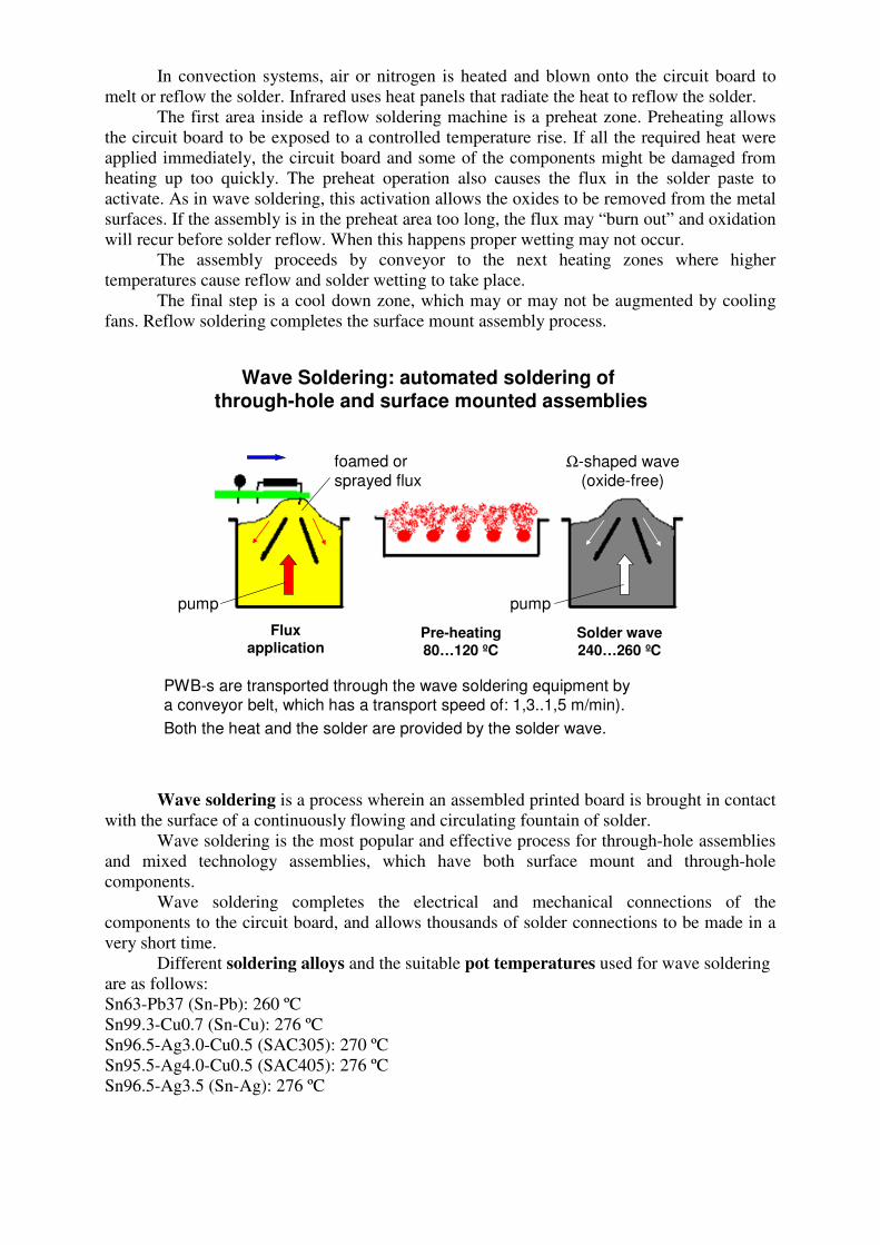
In convection systems, air or nitrogen is heated and blown onto the circuit board to
melt or reflow the solder. Infrared uses heat panels that radiate the heat to reflow the solder.
The first area inside a reflow soldering machine is a preheat zone. Preheating allows
the circuit board to be exposed to a controlled temperature rise. If all the required heat were
applied immediately, the circuit board and some of the components might be damaged from
heating up too quickly. The preheat operation also causes the flux in the solder paste to
activate. As in wave soldering, this activation allows the oxides to be removed from the metal
surfaces. If the assembly is in the preheat area too long, the flux may “burn out” and oxidation
will recur before solder reflow. When this happens proper wetting may not occur.
The assembly proceeds by conveyor to the next heating zones where higher
temperatures cause reflow and solder wetting to take place.
The final step is a cool down zone, which may or may not be augmented by cooling
fans. Reflow soldering completes the surface mount assembly process.
PWB-s are transported through the wave soldering equipment bya conveyor belt, which has a transport speed of: 1,3..1,5 m/min).
Both the heat and the solder are provided by the solder wave.
foamed orsprayed flux
Solder wave
240…260 ºC
Ω-shaped wave(oxide-free)
pump pump
Pre-heating
80…120 ºC
Flux
application
Wave Soldering: automated soldering of through-hole and surface mounted assemblies
Wave soldering is a process wherein an assembled printed board is brought in contact
with the surface of a continuously flowing and circulating fountain of solder.
Wave soldering is the most popular and effective process for through-hole assemblies
and mixed technology assemblies, which have both surface mount and through-hole
components.
Wave soldering completes the electrical and mechanical connections of the
components to the circuit board, and allows thousands of solder connections to be made in a
very short time.
Different soldering alloys and the suitable pot temperatures used for wave soldering
are as follows:
Sn63-Pb37 (Sn-Pb): 260 ºC
Sn99.3-Cu0.7 (Sn-Cu): 276 ºC
Sn96.5-Ag3.0-Cu0.5 (SAC305): 270 ºC
Sn95.5-Ag4.0-Cu0.5 (SAC405): 276 ºC
Sn96.5-Ag3.5 (Sn-Ag): 276 ºC

Integrated Repair Station
Visualization of soldering failures
Integrated shuttle
Marking of component positions
Pictures of the originally detected failures
Storage of error pictures
Reporting of failure class
Repair stations are used to correct and repair recognized soldering failures, with functions as follows:
Fabrication of the LEADOUT boardby lead-free soldering – an example
In the following slides some details of the fabrication of the LEADOUT demonstrator board is presented.
1. Equipment and data of assembly with photos
- stencil printing & stencil design
- assembly – component placement
- reflow soldering
2. Fabrication problems and their effects
- offset of stencil aperture
- solder paste misprint
- imperfect component placement
- paste misprint and smearing

Stencil Printing & Stencil Design
Thieme TES/S-25 stencil printer features:
Printing speed: 20…140 mm/s
Pressure: 10…60 N, angle: 45…90º
Settings during experiment:
Printing speed: 400 mm/s
Pressure: 55 N, angle: 45 º
Stencil:
Laser-cut
150 µm thick
Stainless steel
Inverse home plate apertures for Surface Mount Components
LEADOUT ”lead-free” demonstrator after stencil printing

Assembly – Component Placement
TWS laser quadra features:
Automatic pick & place
2 nozzles
Laser centering
0402 smallest component
0,4 mm smallest pitch size
Testboardused to determine proper
parameters for component placement and soldering
The LEADOUT demonstrator after component placement

Reflow Soldering
ESSEMTECH R006 reflow oven:
Convection with infra heating
Nitrogen atmosphere can be used
Settings: Preheat: 190 °C
(in air) Soak: 200 °C, 160 s
Reflow: 220 °C, 20 s
Green: 3x3 cm copper area Red: 0603 chip R Blue: air
The LEADOUT demonstrator after reflow soldering

Effect of solder paste misprint:wetting corrected misprinting
After stencil printing After reflow soldering
Monitoring the Assembling – Process Examples
Effect of the offset of stencil aperture:wetting pulled back the solder and the SMD
After stencil printing After reflow soldering
Monitoring the Assembling – Process Examples

After component placement After reflow soldering
Imperfect component placement #1:reflow and wetting pulled back the SMD
Monitoring the Assembling – Process Examples
After component placement After reflow soldering
Imperfect component placement #2:reflow and wetting pulled back the SMD
Monitoring the Assembling – Process Examples

After component placement After reflow soldering
Imperfect component placement #3:reflow and wetting pulled back the SMD
Monitoring the Assembling – Process Examples
After component placement After reflow soldering
Paste misprint and smearing:resulted in solder ball formation
Monitoring the Assembling – Process Examples

After component placement After reflow soldering
Paste misprint and smearing:resulted in solder bead formation
Monitoring the Assembling – Process Examples
2. Printed wiring boards2.1 Types and materials of printed wiring boards

The Printed Wiring Board (PWB)
A printed wiring board (or PWB) is used to mechanically support and electrically connect electronic components using conductive pathways, or traces, etched from copper sheets laminated onto a non-conductive substrate.
A printed wiring board (PWB) is a substrate, which is made up of an insulating board
with copper foil tracks on its outer surfaces (sometimes only on one of the outer surfaces,
more often in the form of inner layers as well). The components are fixed to the PWB and
connected to the conductive copper tracks by soldering.
Types and materials of printed wiring boards
Cu layer: 17, 35, 70, (105) µmSubstrate (v): 0,2….3,2 mm
Cu wire
Fiberglass layer
epoxy
Functions:
• Electric connection between component leads
• Fixing components mechanically
Printed wiring:
• Wiring made on resin based insulating board (foil, surface)
• Conductive layer is mainly copper
Substrate (base material):
• Copper foil covered, reinforced resin
v
Insulating substrate
Cu layer
A Printed Wiring Board (PWB) is a substrate, which is made up of an insulating board with copper foil tracks on its outer surfaces.

A printed wiring board (PWB) is a substrate, which is made up of an insulating board with
copper foil tracks on its outer surfaces (sometimes only on one of the outer surfaces, more
often in the form of inner layers as well). When the board is ready discrete components are
assembled to the board. The components are usually fixed to the PWB and connected to the
conductive copper tracks by soldering. Sometimes the chip-on-board technology is used for
the assembly of semiconductor chip components: integrated circuit chips are attached directly
to the board using adhesives and the electrical connections between the contact pads of the
chip and the board are made by micro scale wire bonding (chip-and-wire technology). The
final assembly is named printed circuit (PC), PC card, or surface mounted assembly (SMA).
PWB categories according to the layer structure
• one sided
• double sided
• multilayer
• metal substrate
• metal core
• 3D, MID (Molded
Interconnect Device)
• multiwire
The single-sided boards have only one patterned conductive layer, and are used for very
simple applications.
Nowadays the double-sided PWBs are the most widespread, where there are two conductive
layers in the laminate, on the two outer sides of the board. The tracks formed from the two
conductive layers are interconnected where necessary by plated-through, i.e. metallized holes.
The components are usually assembled onto the board by the insertion of their leads through
the same holes. This process is called through-hole assembly. If surface mounting technology (SMT) is used, where components are assembled onto the surface of the board
without the insertion of the leads into the holes, the holes only serve as interconnections, they
are usually produced with smaller diameters and called vias. Multilayer printed wiring boards contain more than two, typically four-eight conductive
layers. However the number of conductive layers can be twenty or more. Since there are a
significant decrease in the average size of components and an increase of the component
density on the cards, the need for and the production of the multilayer printed wiring boards
are going up.

PWB categories according to types and materials
For circuit cards and modules the rigid printed wiring boards are used, while flexible and rigid-flex printed wirings are popular for the interconnection of cards placed in different position in equipment or of different modules and units.
Rigid printed wiring board Flexible printed wiring board
Rigid - Reinforcing material (paper, fiberglass, polyaramide, metal…)
- Resin (phenol, epoxy, polyimide, PTFE…)
Flexible (polyester, polyimide, PTFE)
The base material, i.e. the insulating board of a rigid PWB is a sheet of laminated
reinforced resin. Large majority of the laminates are produced using phenol or epoxy resins,
and polyimide is also in use for advanced applications. Reinforcing materials include paper,
glass cloth, asbestos, aramid, nylon, and so on. The FR-4 type epoxy-fiberglass (glass cloth)
laminate is the standard for all high technology and professional electronic assemblies, as its
dimensional stability and heat resistance are excellent. Polyimide resins are also used with
fiberglass reinforcement for rigid PWBs, as they retain their flexural strength up to 250 oC or
higher. This value is much higher than the soldering temperatures encountered, and than the
125-170 oC glass transition temperature for epoxy laminates. On the other hand, polyimide
laminates are considerably more expensive than their epoxy equivalents.
For flexible PWBs it is also the polyimide insulating material which is used without
any reinforcement, or with low percentage of filler like quartz powder. In some cases
photosensitive polyimide is used in order to make via formation easier and more economical.
The boards are generally produced with one or both sides covered by a copper foil, and called
copper clad laminates. The foil is produced by electrolytic plating onto a stainless steel drum
slowly rotating in the liquid electrolyte. The side of the foil in contact with the drum is
smooth and shiny whereas the other side is matt and granular. The thickness of the copper foil
most commonly used is 17-35 µm, but for fine line circuits, in order to obtain better resolution,
foils as thin as 5 µm are also in use. The adhesion of the foil to the organic reinforced prepreg
(preimpregnated laminate) is achieved at the lamination stage, by pressing the granular side of
the foil to the resin of the laminate and curing at increased temperature.
Materials of advanced Printed Wiring Boards
Recent developments in PWB base materials have been directed toward improving their
dimensional stability and surface smoothness to allow the definition of smaller features,
reducing their dielectric constant to meet the requirements of high frequency applications, and
replacing glass reinforcement with laser processable materials to make laser drilling easier.

Linear laminates use glass filaments for reinforcement, but instead of being woven the very
thin filaments are placed parallel to form a layer and such layers are oriented alternately
perpendicular one to another to make a smooth reinforcing fabric, reducing the surface
roughness of the final resin impregnated insulating board. Aramid paper reinforced laminates,
using paperlike nonwoven aramid fabric with epoxy resin impregnation, exhibit very good
dimensional stability with near-to-silicon CTE, have a smooth surface, and can be easily
processed by laser.
A new class of base material is opened by the invention of resin-coated copper, where the
copper foil, which serves as both supporting and reinforcing material, is covered by thin resin
layers, resulting in a very thin and smooth laminate of high thermal conductivity.
In rigid PWBs based on polyimide insulating material, and in conventional flexible PWBs as
well, an adhesive layer of acrylate or epoxy resin, is applied to bond the copper foil to the
polyimide base material. Most flexible laminates used for advanced applications like
laminated multichip modules (MCM-Ls), however, are based on adhesiveless polyimide films,
where either a polyimide film is cast onto a copper foil (as in the case of resin-coated copper),
or copper metallization, produced by the combination of vapor deposition and electroplating,
is applied to a polyimide film. With the latter technology a copper conductive layer as thin as
1 µm, or even thinner, can be achieved.
The choice of the appropriate base material for a given application is determined by the
following aspects: electrical and mechanical properties, environmental resistance, price, etc.
For commercial applications cheap phenol resin - paper laminates are usually used. They
have good heat resistance, good mechanical processing properties, but their water absorption
is high, and mechanical strength is low. Nowadays self-extinguishing laminates are produced,
therefore in case of fire gaseous combustible products are formed which extinguish the fire.
The code of substrates with such features identified with the abbreviation FR (Flame
Retardant). Paper based epoxy resin laminates have small dissipation factor and good insulating features
even in wet environment. Mechanically well processable, flexural strength is better, than that
of phenol resin - paper laminates. Through plated holes can also be produced when using this
kind of substrate. Epoxy - fiberglass laminates have superior electrical, mechanical and heat-resistant
properties. Their water absorption is low. They can be through-hole plated. This is the most
frequently used substrate of double sided and multilayer PWBs.
Beside substrates mentioned before, many other kind of laminates are used, because of their
special properties. Such can be low dielectric constant, dissipation factor or good heat
resistance, heat conductivity or low thermal expansion.
In microwave techniques polytetrafluorethylene (PTFE) laminates are often used, because
of their excellent dielectric properties. This material is well known as Teflon. Its use is limited
by its very high price.
Polyimide-fiberglass laminates are also frequently used. They have good isolation properties
and better heat resistivity, than epoxy resin based substrates.

Characteristics of PWB substrates
FR flame retardant
CEM Composite Epoxy Material:Cu
fiberglass
epoxy
paper
Resin phenol epoxy epoxy epoxy
Core material paper paper fibergl./paper fiberglass
Standard (NEMA) FR2 FR3 CEM1 FR4
Flexural strength (N/mm 2) 135 150 330 500
Water absorption (mg) 28 25 10 7
Solderbath resistance (sec) 15-20 25-30 30-40 >120
Adhesion of Cu foil (N/mm) 2,0 2,2 1,7 2,0
Sheet resistance (ohm) 10 11 2x10 11 10 12 >10 12
Cutting properties +++ +++ ++ +
Flammability V0 V0 V0 V0
Price percentages 55 65 80 100
Table below provides information on the main characteristics of base materials of usual
reinforcement/resin combinations. The main parameters include: the glass transition
temperature, Tg, at which the amorphous polymer changes from being in a hard and relatively
brittle condition to being in a viscous or rubbery condition, thus it characterizes the heat
resistance of laminates; and the coefficient of thermal expansion, CTE, which value
numerically describes the dimensional stability.
PWB categories according to pattern resolution
Normal Fine Very fine
Through-hole
mounted:
SMT, COB, MCM-L:
The applicability of a PWB, and, as a consequence, the quality of its conductive pattern can
be characterized by the minimal width and spacing of conductive lines, which value is also
called resolution. The quality of the pattern and the resolution can also be characterized on the
basis of a typical pattern part around two holes next to each other. In a normal (or

conventional) configuration the distance between these holes is the usual 2.54 mm (1/10 inch).
For normal patterns the minimal value of the line width and spacing is 0.3 mm or higher. If
the diameter of the hole is 0.9 mm, there is space only for a single track line between the holes.
For fine patterns the typical line width is around 0.2 mm and if the hole diameter is the same
0.9 mm, two lines can be conducted between two holes. For very fine patterns the resolution
is less than 0.1 mm, and the hole diameter can be 0.3 mm or less, if necessary, so more than
two conductive lines can be placed between the holes. PWBs with fine and very fine pattern
resolutions, however, are more frequently used for surface mounting technology (SMT),
therefore the characteristic resolution patterns are from SMT boards.
• electrical connection between certain conducting layers
• more reliable soldered joints when using through-hole mounted components
Aim of the through-hole metallization
Through-hole with metallized
wall
Nonmetallized holes with round, rectangular or any other shape are used for fixing
components onto the board either by inserting the component leads through them or by using
surface mounting technology (SMT) or chip-on-board (COB) assembling methods. The
metallized holes are used not only for through-hole assembling the components, but for
producing interconnections between the tracks of different conductive layers. Vias are not
intended to insert component leads into them, they are only interconnections, electrically or
thermally joining different conductive layers of a multilayer structure. A through-board via
connects both outer layers and, not necessarily, inner layer(s). A blind via connects an outer
layer and at least one inner layer, but does not connect both outer layers. A buried via makes
interconnection between only inner layers of the board. The aim of a thermal via is to conduct
heat from a component heat source to a heat sink layer of the structure.

delamination
Typical through-hole failures
barrel crack
corner crackpad rotationmissingplating
pad lifting
nodule
pull away
break betweenlayer and plating
plating voidmisalignmentof PCB duringdrilling
imprecisefitting
2. Printed wiring boards2.2 Mechanical technologies in PWB-production
Mechanical technologies in PWB-production
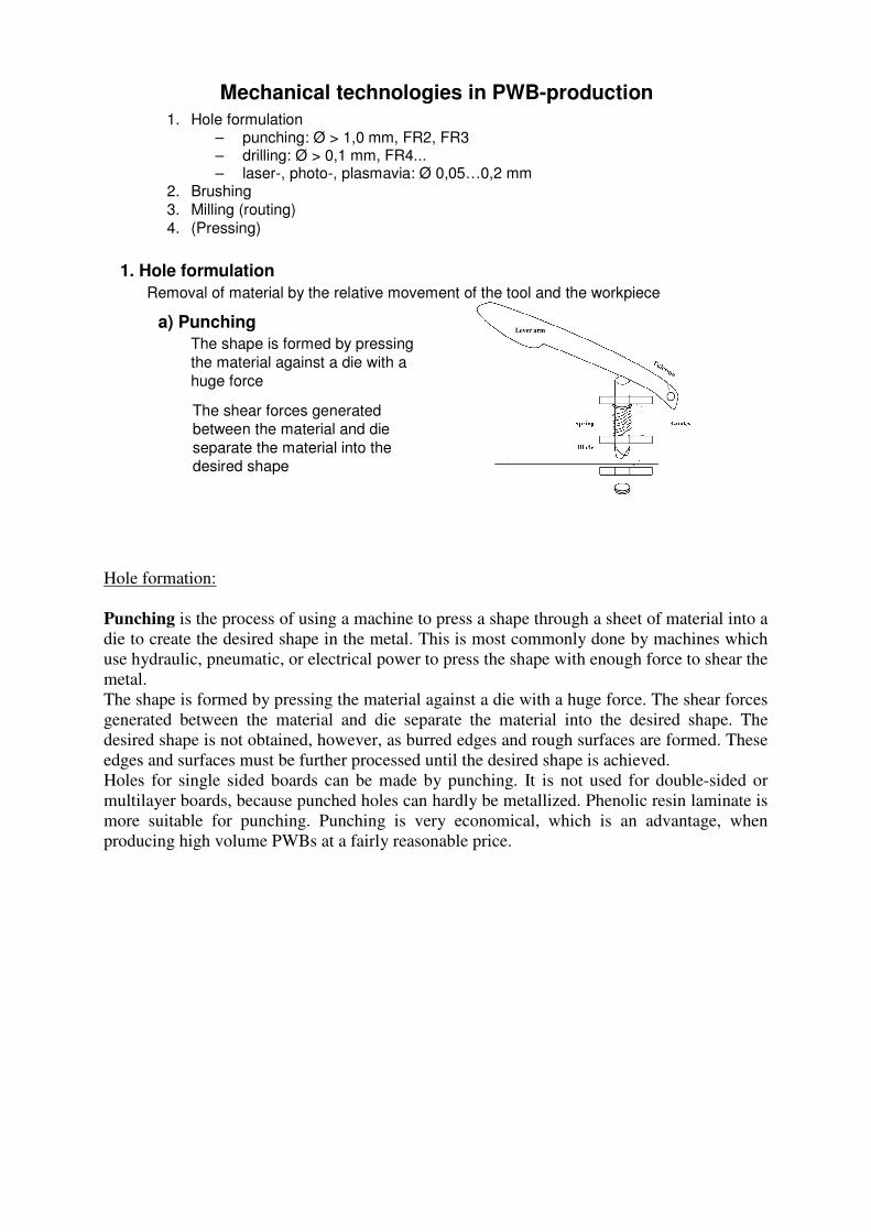
1. Hole formulation– punching: Ø > 1,0 mm, FR2, FR3– drilling: Ø > 0,1 mm, FR4...– laser-, photo-, plasmavia: Ø 0,05…0,2 mm
2. Brushing3. Milling (routing)4. (Pressing)
1. Hole formulation
a) Punching
The shape is formed by pressing the material against a die with a huge force
The shear forces generated between the material and die separate the material into the desired shape
Removal of material by the relative movement of the tool and the workpiece
Hole formation:
Punching is the process of using a machine to press a shape through a sheet of material into a
die to create the desired shape in the metal. This is most commonly done by machines which
use hydraulic, pneumatic, or electrical power to press the shape with enough force to shear the
metal.
The shape is formed by pressing the material against a die with a huge force. The shear forces
generated between the material and die separate the material into the desired shape. The
desired shape is not obtained, however, as burred edges and rough surfaces are formed. These
edges and surfaces must be further processed until the desired shape is achieved.
Holes for single sided boards can be made by punching. It is not used for double-sided or
multilayer boards, because punched holes can hardly be metallized. Phenolic resin laminate is
more suitable for punching. Punching is very economical, which is an advantage, when
producing high volume PWBs at a fairly reasonable price.

b) Drilling
Primary movement: rotation of drill → cutting speed (v, m/min)
Secondary movement: perpendicular to the surface
→ feedrate (f, mm/rot.)
• the material of workpiece• the material of tool and it's geometry• the speed components of relative movement (main-
and side movements)
Dominant factors:
Composition:
Mechanical technologies in PWB-production
• 88...94 % tungsten carbide (WC)• 6...12 % cobalt (Co)
Drilling is one of the most critical processes of PWB manufacturing. During drilling, the drill
bit reaches hundreds of oC. This melts the epoxy resin and smears it around the inside of the
hole. For double sided boards this can be a problem because electroless copper will not adhere
well to smeared epoxy. Smear inside the hole is even more problematic when producing
multilayer boards. This type of board has layers of circuitry laminated together. Electrical
connections are made with the inner layers by the plated hole. If the plating is done on top of
epoxy smear, no electrical connection can be made. The drill bit must be hard and sharp. A
dull drill bit can create the problem of having to deposit over loose bundles of glass fibers. It
is difficult to get adequate coverage in cases like this.
Drill package formulation
Entry plate:• preventing of abrasion• preventing of burring• increase of hole position
accuracy• increase of hole wall qualityBackup plate:• preventing of burring• protecting of CNC working table
Entry plate
Backup plate
HoleSubstrates
Mechanical technologies in PWB-production
For CNC drilling, packet should be prepared. The FR4 epoxy fiberglass substrate, the entry
and backup plates are cut to size and fitted together with 3mm diameter pins. The entry plate
is a 0,24mm thick aluminium plate. For backup 2,5 mm thick plate is used made from resin
and wood fibre. For increasing productivity, more substrates are put together, and drilled at
the same time (Figure 1.). The number of substrates, which can be drilled in the same packet,
is determined by the ratio of the length of the hole and the diameter of the hole, this ratio
should not be more than 7-8 in practice. The aim of entry and backup plates is to avoid burr
formation. The backup plate is intended to protect the work table of CNC also. Set-up of the
packet followed by drilling with CNC machine.
The packet is fixed on the working table by the help of pneumatic device built in the table,
which clamp the two pins. The drill spindle and table is moved by servomotors in the
direction of the three axes. Chips generated during the operation of CNC are removed by the
exhaust system.
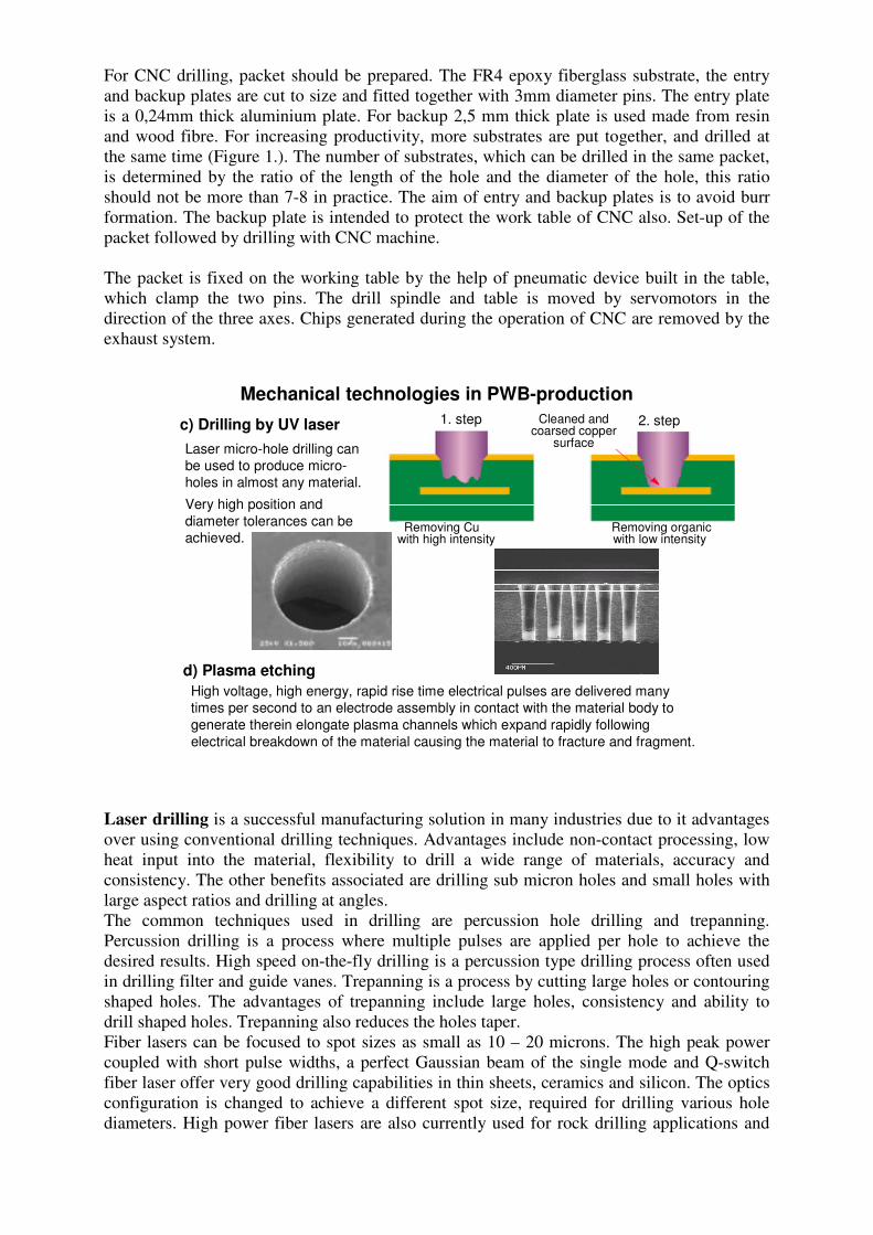
c) Drilling by UV laser
Laser micro-hole drilling can be used to produce micro-holes in almost any material.
Very high position and diameter tolerances can be achieved.
1. step 2. step
Removing Cu Removing organicwith high intensity with low intensity
Cleaned and coarsed copper
surface
d) Plasma etching
High voltage, high energy, rapid rise time electrical pulses are delivered many times per second to an electrode assembly in contact with the material body to generate therein elongate plasma channels which expand rapidly following electrical breakdown of the material causing the material to fracture and fragment.
Mechanical technologies in PWB-production
Laser drilling is a successful manufacturing solution in many industries due to it advantages
over using conventional drilling techniques. Advantages include non-contact processing, low
heat input into the material, flexibility to drill a wide range of materials, accuracy and
consistency. The other benefits associated are drilling sub micron holes and small holes with
large aspect ratios and drilling at angles.
The common techniques used in drilling are percussion hole drilling and trepanning.
Percussion drilling is a process where multiple pulses are applied per hole to achieve the
desired results. High speed on-the-fly drilling is a percussion type drilling process often used
in drilling filter and guide vanes. Trepanning is a process by cutting large holes or contouring
shaped holes. The advantages of trepanning include large holes, consistency and ability to
drill shaped holes. Trepanning also reduces the holes taper.
Fiber lasers can be focused to spot sizes as small as 10 – 20 microns. The high peak power
coupled with short pulse widths, a perfect Gaussian beam of the single mode and Q-switch
fiber laser offer very good drilling capabilities in thin sheets, ceramics and silicon. The optics
configuration is changed to achieve a different spot size, required for drilling various hole
diameters. High power fiber lasers are also currently used for rock drilling applications and

for oil and gas exploration industries. The high peak and energy /pulse are also used for
drilling thick metals.
Plasma etching: Material is removed from a body of material, e.g. to create a bore hole, by
plasma channel drilling. High voltage, high energy, rapid rise time electrical pulses are
delivered many times per second to an electrode assembly in contact with the material body to
generate therein elongate plasma channels which expand rapidly following electrical
breakdown of the material causing the material to fracture and fragment.
2. Brushing
The brushing mashine containsrotating brushes with variouscorning and a conveyor systemfor feeding the board into them.
For better efficiency the boardsare continuously washed bywater spraying
3. Milling (routing)
In contrast to drilling, where the drill is moved exclusively along its axis, the milling operation involves movement of the rotating cutter sideways as well
Milling is the process of cutting away materialby feeding a workpiece past a rotating multipletooth cutter
Mechanical technologies in PWB-production
Click on the figure to start movie!
Brushing: The first step in surface finishing is the brushing of drilled boards. The board must be free of
burr, caused by drilling. Brushing is used to clean the surface of laminate, to set the necessary
surface structure, roughness, and to make a smooth surface, having no burrs. PWB is
scrubbed after drilling, before plating, before photoresist mask preparation, and before contact
finger plating. Scrubbing is usually made by conveyor machines, containing rotating and
oscillating brushes. The brushing mashine contains rotating brushes with various corning and
a conveyor system for feeding the board into them. For better efficiency the boards are
continuously washed by water spraying. Water is applied to cool the brushes, the laminate and
to carry away the removed particles. This process removes not only burrs, but other
contaminations as well.
Milling (routing): CNC routing is used to get the exact shape and dimensions of the PWB. A milling machine
is a tool used for shaping solid materials. Its basic form is a rotating cutter which rotates
around the spindle axis (similar to a drilll), and a table to which the workpiece is fixed. In
contrast to drilling, where the drill is moved exclusively along its axis, the milling operation
involves movement of the rotating cutter sideways as well as vertically. The cutter and
workpiece move relative to each other, generating a toolpath along where material is removed.
The movement is precisely controlled, usually with slides and lleadscrews or analogous
technology. Often the movement is achieved by moving the table while the cutter rotates in
one place. Milling machines can be operated manually or by CNC (Computer Numerical
Control).

2. Printed wiring boards2.3 Chemical technologies in PWB-production
Chemical technologies in PWB-production
The chemical technologies include the cleaning, layer deposition, layer removal, surface finishing and rinsing processes.
The most important electrochemical and electroless layer deposition processes are based on the same principle: on reduction.
Me n+ + ne - = Me (reduction)
1. Electroplating +_
Men+Can be applied only onto conductive surfaces, for selective coatings it is not suitable.
Electroplating: In this process electrical current is used to reduce cations of a desired material from a solution
and coat a conductive object with a thin layer of the material.
The part to be plated is the cathod of the circuit. The anode is made of the metal to be plated
on the part. Both components are immersed in a solution (called electrolyte) containing one or
more dissolved metal salts and other ions that permit the flow of electricity. A rectifier
supplies a direct current to the cathode causing the metal ions in the electrolyte solution to
lose their charge and plate out on the cathode. As the current flows through the circuit, the
anode slowly dissolves and replenishes the ions in the bath.

Electroplating is primarily used for depositing a layer of material to bestowe a desired
property (e.g., abrasion and wear resistance, corrosion protection, lubricity, aesthetic qualities,
etc.) to a surface that otherwise lacks that property. Another application uses electroplating to
build up thickness on undersized parts.
2. electroless deposition
3. „direct plating”
after deposition of conductive chemical compound onto the insulator surface it can be electroplated
4. immersion deposition
Me1n+
Me2
−+
+⇒ kekMe2Me2
Me1neMe1n⇒+
−+
- for catalytic insulators- purpose is to metallize the isolating wall of drilled holes
Men+ + reducing material = Me
e.g. CuSO4 + 4NaOH + 2HCHO = Cu+2HCOONa + Na2SO4 + H2 + 2H2O
Chemical technologies in PWB-production
The purpose of the electroless copper deposition process is to metallize the isolating
wall of drilled holes. This metallization provides an electrical connection between the sides of
a panel, and to the inner layers of multilayer boards.
Before electroless copper process, the drilled PWB is mechanically and chemically
cleaned by scrubbing, removing of grease, micro-etching and oxide-removing.
The surface of the PWB must be activated. Activating is necessary, because the copper
coating must be deposited onto the isolating surface of epoxy-resin. After this stage PWB is
ready to metallization, which usually means through-hole plating.
The electroless copper deposition process is based on the chemical reduction of
copper initialized by the activating particles. Slow operating type of electroless copper bath is
used to deposit a very thin, but continuous layer of copper. Electroless copper layers,
deposited from a room temperature bath, are only ca 1 micrometer thick. The advantage of
this type of bath is the careless operation. When using slow operating type of electroless
copper bath, the thin coating of electroless copper is thickened by electroplating. In this way
the copper coating being inside the holes is formed by a two-stage depositing process:
electroless copper followed by electroplating. By using quick operating electroless copper
bath, it is possible to deposit the copper coating by a single-stage process, without
electroplating.
Immersion deposition: The process needs neither power supply nor reducing agent. The
material of work piece (Me2, it can be only metal) oxidizes, i.e. transmits its electrons to
Me1n+ which will be reduced and deposited on the surface of work piece. The condition of
the process is that the normal potential of Me2 is more negative than that of M1. It means,
that only certain metals can be coated using this process.
2. Printed wiring boards2.4 Patterning processes of PWBs: Masking technologies
Masking technologies
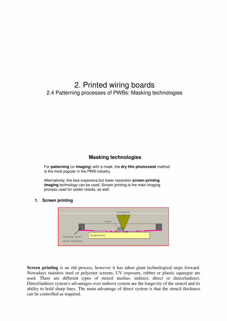
1. Screen printing
For patterning (or imaging) with a mask, the dry film photoresist method is the most popular in the PWB industry.
Alternatively, the less expensive but lower resolution screen printing
imaging technology can be used. Screen printing is the main imaging process used for solder resists, as well.
Screen printing is an old process, however it has taken giant technological steps forward.
Nowadays stainless steel or polyester screens, UV exposure, rubber or plastic squeegee are
used. There are different types of stencil medias: indirect, direct or direct/indirect.
Direct/indirect system's advantages over indirect system are the longevity of the stencil and its
ability to hold sharp lines. The main advantage of direct system is that the stencil thickness
can be controlled as required.
Lot of manufacturers have automatic screen printers. Advantages to using this type of
equipment are:
- the pressure used during the printing is uniform and consistent;
- the squeegee angles with respect to the surface of the panel is consistent;
- the throughput is higher.
In the PWB industry etching resists, plating resists, solder resists and legend resist are applied
by screen printing.
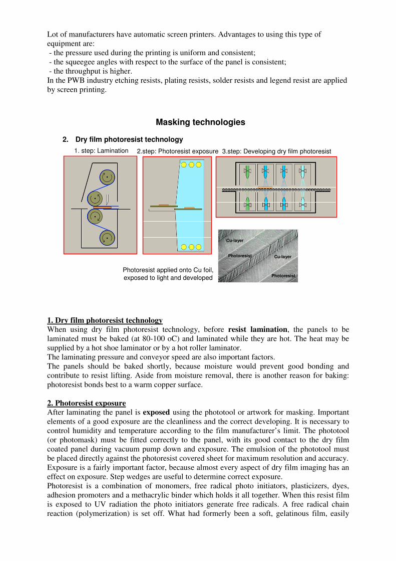
Masking technologies
Photoresist applied onto Cu foil,exposed to light and developed
Cu-layer
Photoresist
Cu-layerPhotoresist
3.step: Developing dry film photoresist
2. Dry film photoresist technology
2.step: Photoresist exposure1. step: Lamination
1. Dry film photoresist technology When using dry film photoresist technology, before resist lamination, the panels to be
laminated must be baked (at 80-100 oC) and laminated while they are hot. The heat may be
supplied by a hot shoe laminator or by a hot roller laminator.
The laminating pressure and conveyor speed are also important factors.
The panels should be baked shortly, because moisture would prevent good bonding and
contribute to resist lifting. Aside from moisture removal, there is another reason for baking:
photoresist bonds best to a warm copper surface.
2. Photoresist exposure After laminating the panel is exposed using the phototool or artwork for masking. Important
elements of a good exposure are the cleanliness and the correct developing. It is necessary to
control humidity and temperature according to the film manufacturer’s limit. The phototool
(or photomask) must be fitted correctly to the panel, with its good contact to the dry film
coated panel during vacuum pump down and exposure. The emulsion of the phototool must
be placed directly against the photoresist covered sheet for maximum resolution and accuracy.
Exposure is a fairly important factor, because almost every aspect of dry film imaging has an
effect on exposure. Step wedges are useful to determine correct exposure.
Photoresist is a combination of monomers, free radical photo initiators, plasticizers, dyes,
adhesion promoters and a methacrylic binder which holds it all together. When this resist film
is exposed to UV radiation the photo initiators generate free radicals. A free radical chain
reaction (polymerization) is set off. What had formerly been a soft, gelatinous film, easily

washed away by the developing solvent, has now become a hard, chemically resistant surface,
suitable as plating or etching resist.
3. Developing The unexposed resist is washed away in conveyorized or non-conveyorized developer.
Nowadays, fully aqueous developing photoresists are in use to meet the environment
protection requirements.
The advantages of dry film photoresist are as follows:
-fine lines definitions;
-plated circuitry has straight sidewalls;
-excellent conformance to artwork dimensions;
-fast set up and turnaround time on small jobs;
-hole tenting provides a photoresist seal over a hole, so it eliminates the need of hole plugging.
The following disadvantages should be mentioned:
-dry film photoresist is expensive to buy;
-large capital investment is required to purchase processing equipment;
-dry film leaves a monomolecular layer of adhesion promoter on the copper surface from
which it has been developed, and this layer must be chemically etched off. The key steps of
dry film --photoresist processing: lamination, exposure, developing.
2. Printed wiring boards2.5 Fabrication of single sided boards using
subtractive or additive technology

Processing possibilities:
• Subtractive technology
The raw material is a dielectric plate with copper cladding on one or both sides. The copper layer is removed (usually by chemical etching) where the wiring is not needed.
The resolution is limited by the adhesion of the conducting layer and the undercutting effect.
• Additive technologyThe conducting layer is deposited on the insulating substrate in a particular pattern using a mask.
It results in finer resolution but worse adhesion.
• Semi-additive technology
It combines the advantages of both previous technologies
Fabrication of single sided boards using
subtractive or additive technology
There are two main types of manufacturing processes of PWBs.
The subtractive process uses copper clad laminates and subtracts the unnecessary pattern of
copper layer from the surface by etching.
In the course of the additive process the wiring pattern is deposited physically, chemically or
mechanically onto the originally insulating surface of the board.
The most popular board fabrication sequences are based on the subtractive process, however
they contain additive steps as well. The main advantage is the excellent adhesion of the
copper foil to the insulating board. The additive process is typical for thick film technology
using ceramic substrates.
There is also a combination of the two processes, the semi-additive process: it starts from
laminates covered by thin copper foils, then uses additive process steps and differential
etching, resulting in very fine pattern.

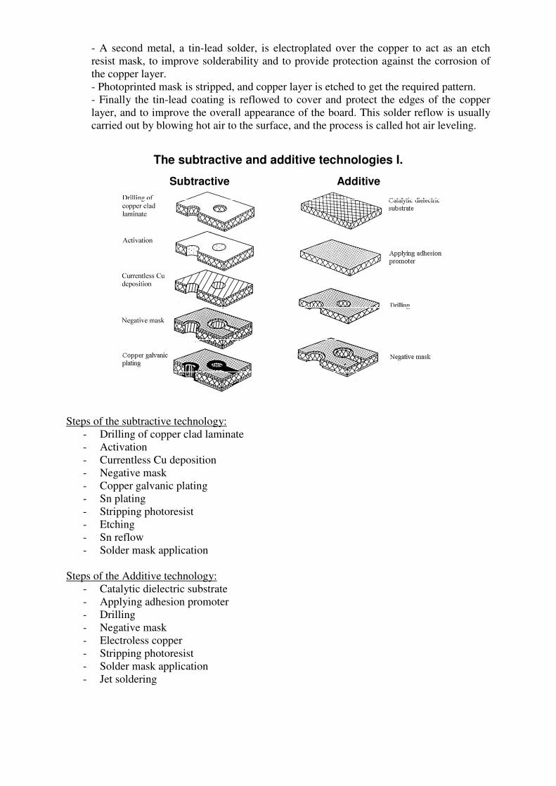
The subtractive and additive technologies
Subtractive Additive
Cu foil covered insulating board Insulating board
Electroless metallization, Positive mask(screenprinting, photoresist, metal)
Negative mask(screenprinting, photoresist)
Etching, mask stripping Electroless metallization, mask stripping
The subtractive process uses copper clad laminates and subtracts the unnecessary pattern of
copper layer from the surface by etching.
In the course of the additive process the wiring pattern is deposited physically, chemically or
mechanically onto the originally insulating surface of the board.
Subtractive technology of single sided PWBs
Base material: copper foil covered insulating board
Undercutting Mushroom effectMask removal
[Removing metal mask („orange effect”)]
Negative mask(photoresist, screen printing)
Positive mask(photoresist, screen printing)
Etching Positive metal mask (Sn, Sn/Pb…)
Etching
Solder mask
wire pad
Positive mask: Starting with a copper clad laminate, the pattern of the wiring is screen printed onto the
surface as a positive mask. Alternatively photoresist technology can also be used to make the
same mask, but the much cheaper screen-printing is sufficiently good for the rough resolution
of common single-sided boards. From the uncovered places the copper foil is removed by
etching, then the mask layer is stripped, and in the last step the holes are drilled.
Negative mask

2. Printed wiring boards2.6 Subtractive technology of double sided, through-
hole metallized boards
Subtractive technology of double sided, through-hole metallized boards
This sequence includes main groups of processing steps as follows:
- Starting with a double-sided copper clad laminate, at first holes are fabricated by
drilling, then they are deburred and cleaned.
- The panels are sensitized and an electroless copper flash is given to make the holes
conductive for electroplating.
- A plating resist negative mask is produced by the following steps: dry film resist
lamination, transferring the image by through photo-mask UV light exposure and
development.
- A pattern of copper layer is electroplated to the uncovered areas. The minimum
thickness of the copper layer required in the holes is usually 20 µm. (At this point it
should be mentioned, that a modern electrochemical process called direct plating is also
in use. It substitutes electroless plating and electroplating, thus simplifies the processing
sequence. The modified sensitizing step prior to the direct plating process makes the
surface slightly conductive, which launches the electroplating process directly.)
- A second metal, a tin-lead solder, is electroplated over the copper to act as an etch
resist mask, to improve solderability and to provide protection against the corrosion of
the copper layer.
- Photoprinted mask is stripped, and copper layer is etched to get the required pattern.
- Finally the tin-lead coating is reflowed to cover and protect the edges of the copper
layer, and to improve the overall appearance of the board. This solder reflow is usually
carried out by blowing hot air to the surface, and the process is called hot air leveling.
The subtractive and additive technologies I.
Subtractive Additive
Steps of the subtractive technology:
- Drilling of copper clad laminate
- Activation
- Currentless Cu deposition
- Negative mask
- Copper galvanic plating
- Sn plating
- Stripping photoresist
- Etching
- Sn reflow
- Solder mask application
Steps of the Additive technology:
- Catalytic dielectric substrate
- Applying adhesion promoter
- Drilling
- Negative mask
- Electroless copper
- Stripping photoresist
- Solder mask application
- Jet soldering

Electroless
copper
The subtractive and additive technologies II.
Subtractive Additive
Sn plating
Sn reflow
Steps of the subtractive technology:
- Drilling of copper clad laminate
- Activation
- Currentless Cu deposition
- Negative mask
- Copper galvanic plating
- Sn plating
- Stripping photoresist
- Etching
- Sn reflow
- Solder mask application
Steps of the Additive technology:
- Catalytic dielectric substrate
- Applying adhesion promoter
- Drilling
- Negative mask
- Electroless copper
- Stripping photoresist
- Solder mask application
- Jet soldering

Semi-additive technology
A possible way of producing the substrate
Semi-additive technology can be applied for manufacturing PWBs to improve their
resolution. The base material for this technology is copper-clad laminate with very thin, 5 m
or thinner, copper layer, temporarily covered by a 70 m thick Al or Cu protective layer. This
protective layer served as substrate when the thin copper layer was electroplated and
laminated, and it can be easily peeled off before further processing. Additive processes,
selective copper electroless- and electroplating into the windows of a thick photoresist layer
are used for image definition to get high resolution pattern with perpendicular edges. After
stripping the photoresist layer, a subtractive process, differential etching is applied to remove
the thin parts of the copper layer, while the thickness of the electroplated areas only slightly
decreases. Since the inaccuracy of etching is proportional to the very low etched thickness,
the resolution of the final pattern is much better than that is provided by the usual pattern or
panel plating technologies.

2. Printed wiring boards2.7 Technology of co-laminated multilayer printed
wiring boards
Technology of co-laminated multilayer printed wiring
boards
Each inner layer must be patterned and the surface of the Cu must be prepared for gluing (Sn stripping if necessary, oxidization)
The inner boards can have through holes that will become buried vias in the multilayer board.
Co-lamination technology: the boards are glued together with preimpregnated (prepreg) B-stage
epoxy foil.
Needs at least 30...60 minutes on 170 oC, at 150 N/cm2 pressure.
Multilayer printed wiring boards contain typically 4 to 20 conductive layers. Since there
are a significant decrease in the average size of components and an increase of the component
density on the cards, the need for and the production of the multilayer printed wiring boards
are going up.
The number of layers is determined by the number of conducting layers.
The manufacturing of multilayer printed wiring boards contains three separate process
sequences: at first the panels with the inner conductive layers are produced by simple double-
sided etching from copper clad prepreg laminates; then these etched panels, adhesive prepregs
and unetched outer panels are laminated, pressed and cured (heat treated) to get a rigid board;
and at last this board is processed by a sequence corresponding to pattern or panel plating of
double-sided boards.
The special and most important steps of this usual manufacturing process of multilayer
PWBs involve the lamination of etched and unetched panels. Any combination of single-sided
and double-sided prepreg panels can be used to form the required multilayer structure, with
the only condition that all inner layers must be patterned before lamination.
Cu plating
Sn/Pb plating
resist stripping
Cu etching
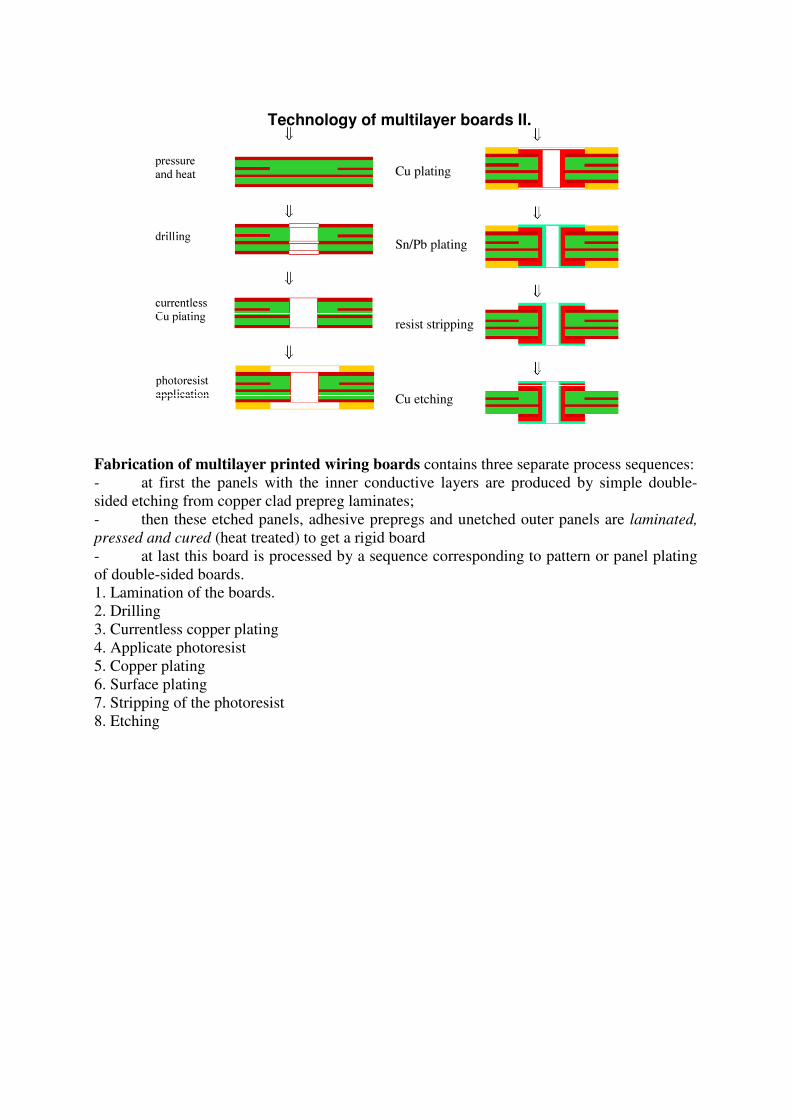
Technology of multilayer boards II.
Fabrication of multilayer printed wiring boards contains three separate process sequences:
- at first the panels with the inner conductive layers are produced by simple double-
sided etching from copper clad prepreg laminates;
- then these etched panels, adhesive prepregs and unetched outer panels are laminated,
pressed and cured (heat treated) to get a rigid board
- at last this board is processed by a sequence corresponding to pattern or panel plating
of double-sided boards.
1. Lamination of the boards.
2. Drilling
3. Currentless copper plating
4. Applicate photoresist
5. Copper plating
6. Surface plating
7. Stripping of the photoresist
8. Etching

Via types and layers of multilayer boards
Vias are plated-through holes on two-sided and multilayer boards that are used to interconnect
layers or traces, but they are not used for component mounting. Vias are usually smaller in
diameter than component holes. There are two special types of vias:
1. Blind vias. Blind vias are visible from one exterior side of the board. The other end of blind
vias terminate on interior layers.
2. Buried vias. Buried vias are not visible from an exterior layer of the board. They connect
conductive layers in the interior of the PCB.
Sequential technology with wall-metallized vias
• Sequential build-up (SBU) technology:
A multilayer board is created by applying conductive and insulating layers one after each other.
Sequential build-up (SBU) technology:
A multilayer board is created by applying conductive and insulating layers one after each other.
Multilayer boards are produced by applying layers one after the other.

Producing layers connected by vias:
• Applying metallized vias
• Applying column vias
• Advantages of microvias
• Examples presenting the technological process:
• laminating and drilling by laser or plasma
• using photosensitive dielectrics
• Combining thin-film technologies and chip attachment on flexible substrates
Advantages of microvias: • Shorter wires (higher speed)
• Smaller number of layers
• Smaller size
• CSP and BGA packages can be used
• Smaller parasitic effects (lower noise)
• Better thermal conductivity
• Improved reliability
• Lower cost
Sequential build up (SBU) technology
Comparison of structure of different microvias
Laser
Plasma
Drilling
The low cost photo via processing requires layers of photoimageable dielectric materials.
These photosensitized polymers, mainly on polyimide or epoxy basis, work like photoresists:
after having been exposed through a mask, the vias and windows of any geometry defined by
the mask can be developed. Curing is used to improve the dielectric properties of the
materials.
Plasma-etched via (PEV) technology applies vacuum process to remove the polyimide
dielectric layer. All vias for one layer are generated simultaneously. The previously patterned
copper layer serves for masking, i.e. the polyimide is etched through the openings of the
copper layer, etching automatically stops at the inner copper layer. Blind vias can be
generated from any side of the board. Typical via holes are 60-90 µm in diameter and require
200-300 µm capture pads. Regarding the processed geometry, PEV is a very flexible process:

in addition to through and blind vias it can create slots, windows, stepped windows (using
controlled etch time), slanted vias and unique structures as well.
An alternative technology is laser via generation. Similarly to PEV, laser vias can be
generated through polymer films applying the patterned copper layer for masking by exposing
the entire surface with UV excimer lasers, or by punching, one hole after the other, using a
frequency multiplied UV Nd:YAG defocused laser beam. PEV and excimer laser via
generation technologies need expensive equipment, however, they can be economic for mass
production. Nd:YAG laser technology has the advantage that copper layers can also be
processed with focused beam by trepanning along the hole perimeter. Blind vias can also be
generated by the combination of focused beam spiraling and defocused beam punching. In
general, it is less effective, but more flexible; it is preferred for prototyping or smaller batch
manufacturing.
Any of these three processes can be used for via hole generation in the pastevia process. After
the holes are opened into a single dielectric layer, they are filled with conductive paste. The
copper foils are laminated and photo-imaged later on the dielectric layer. The complete board
is finally prepared by co-lamination and curing.
All four via preparation and wall metallization methods have particular advantages:
- photovia technology is very productive, resolution is high, but provides irregular hole
wall quality, and needs special photodielectric materials;
- plasmavia process provides even hole uniformity and cleanliness, it is productive, but
needs expensive equipment;
- laser via drilling provides very clean surface and suitable wall shape, it is very flexible,
but less economic than photovia processing;
- paste vias are very cheap, but less reliable than wall metallized vias.
2. Printed wiring boards2.8 Special printed wiring boards and their technologies

Technology of Metal Substrate PWB-s
•Metal core covered with insulating layer and a copper
foil on the outer surface.
Aim: to achieve better heat conductivity
• epoxy-woven fiber glass board: 0.2 W/mK,
• IMS boards: 1.3 W/mK.
IMS = Insulated Metal Substrate
Formulation of the pattern by subtractive
technology:
drilling of the metal plate, filling the hole with
epoxy enriched with Al2O3,
drilling of the epoxy, metallization of the holes
For Insulated Metal Substrates bare metal sheet base materials are used. At first larger holes
are drilled into the metal sheet; liquid epoxy is used to fill up the holes and cover the surfaces
on both sides; the required diameter holes are drilled; and finally additive electroless plating
combined with photoresist processing and etching is applied for copper deposition and
patterning.
•Aim: to minimize the thermal expansion mismatch between the substrate and the components / to adjust the thermal expansion coefficient of the substrate to that of the components
Thermal expansion coefficient:
• epoxy-woven fiberglass 12..16 ppm/°C• CCC encapsulation 5.9…7.4 ppm/°C
Metal Core PWB
CCC = Ceramic Chip Carrier
V=0.12..1.5 mm
Core materials (≈≈≈≈ 5 ppm/°C):• Cu-Mo-Cu (CMC)
• Cu-Invar-Cu (CIC)
Metal core printed boards have the advantages of both lower thermal expansion and higher
heat dissipation. An approach can be to laminate single-sided boards onto each sides of a
metal sheet with low CTE, like invar. The holes, that should be insulated from the metal core,
are prepared by the following process sequence: drill larger than required holes; fill up the
holes with epoxy resin and cure; and drill holes to the same positions with required diameter.
Then the usual double-sided PWB technology can be applied.

Flexible PWBs
Two possible ways of manufacturing:1. Cu foil laminated onto the plastic,2. Plastic is deposited onto the Cu foil(the more
up-to-date technology).
Materials: plastic (polyimide
- Kapton, polyester - Mylar,
PTFE - Teflon)
foil without rreinforcement
Available in single-, double- and multilayer construction as well.
Application: connecting moving elements,vibration tolerating devices (due tosmaller mass), 3D interconnection systems.
Flexible printed wirings are used for cables to electrically interconnect distant or moving
boards or modules; for foil keyboards to overpass level or angle deviations; for three
dimensional modules to be realised on a single board, etc.
For flexible PWBs it is the polyimide insulating material which is used without any
reinforcement, or with low percentage of filler like quartz powder. In some cases
photosensitive polyimide is used in order to make via formation easier and more economical.
The boards are generally produced with one or both sides covered by a copper foil, and called
copper clad laminates. The foil is produced by electrolytic plating onto a stainless steel drum
slowly rotating in the liquid electrolyte. The side of the foil in contact with the drum is
smooth and shiny whereas the other side is matt and granular. The thickness of the copper foil
most commonly used is 17-35 µm, but for fine line circuits, in order to obtain better resolution,
foils as thin as 5 µm are also in use. The adhesion of the foil to the organic reinforced prepreg
(preimpregnated laminate) is achieved at the lamination stage, by pressing the granular side of
the foil to the resin of the laminate and curing at increased temperature.

Rigid-flex combined PWB
Adhesive foil
Wiring pattern
Metallized holes
Metallized through holes
Flexible substrate
Rigid substrateRigid
substrate
Rigid and flexible PWB technologies can be combined, as in the rigid-flex board, where a
flexible board is laminated into rigid multilayer boards forming the inner layers of them.
Technologies based on copper clad laminates and on polymer thick films both are in use for
the manufacturing of flexible interconnections and rigid-flexible combinations.
Rigid-flex circuit boards provide opportunity for building higher component density modules
of 3-D folded configurations in size-limited applications. They are also used in pocket
calculators, laptop computers, mobile phones and similar lightweight, portable electronic
equipment, where there are folding p
arts containing electronics on the rigid boards interconnected by the in-built flexible wiring.
The technology of a multilayer rigid-flex printed circuit board usually starts with the
preparation of a flexible double-sided foil, which will serve as flexible part of the board and
inner layers of the rigid parts as well. It is followed by lamination of rigid prepregs, but not
onto the entire surface, thus leaving flexible areas in the board. The further steps are
conventional multilayer PWB processes.

3D MIDs (Molded Interconnection Devices)
Interconnection is produced by applyingthe wiring onto the surface of the plasticdevices.
• Metallization of the plastic:electroless Cu deposition.
• Applying the photoresist:
by electrophoresis
• Exposure:direct writing by laserexposure applying of 3D fotomask
The 3D wiring may replace some mechanical components, like touch
switch components
SMD
Shock resistant plastic, e.g. PEI=polyetherimid
A possible approach for the increase of wiring density of PWBs is the application of real
three-dimensional (3D) construction. The edges of a traditional multilayer board are ground to
get clear metallic cross surfaces of the printed wires, which are intentionally led to the rim of
the board. Then the edges are electroless copper plated or covered by copper using any other
edge-contacting process. An appropriate insulating pattern is cut by laser direct writing to
prepare tracks between the lines on surfaces and inner layers.
Another popular 3D construction is a molded case of any shape with patterned conductive
layer, which follows the 3D shape of the inner surface of the case. The pattern can be
prepared by electroless copper deposition, photolithography and etching. Alternatively, the
surface is spread with silver powder, and a hot photogravure tool is used to press and fix the
pattern onto the surface while the powder can be removed from the unpressed areas.

Multiwire PWB
Multiwire PWB: combining the PWB technology with the conventional wiring. Metallised through holes are made after sticking insulation covered wires into the cover prepreg film.
Multiwire interconnection boards combine double- or multilayer structures with insulated
wires embedded in a prepreg layer laminated onto one of the outer surfaces of the board. Wire
diameters are typically in the range of 80-100 m, having similar current load capacity as that
of 35 m thick and 0.15-0.25 mm wide printed tracks. The wires are laid prior to curing the
prepreg layer and drilling the holes. Since insulated wires are used, crossovers can be easily
prepared. If a wire terminates in or crosses the drilling area of a hole, it will be cut by drilling,
providing a contact surface for through-hole-plated interconnection. In this way high density
interconnection substrates with simple and flexible design capability can be fabricated.
Wire peaces are laid down (pressed into) the B-stage prepreg laminated onto the substrate
between the through-holes to be drilled later.
After that the epoxy layer will be cross-linked (solidified). Then the board will be drilled and
the holes will be metallised.
The wires are connected to the electric circuit through the metallised through-holes.
Advantages of multiwire PWBs: can be applied on high component density boards,
the number of holes can be decreased.
Surface finishes used on printed wiring boards
4.1 Surface Finishes of Printed Wiring Boards
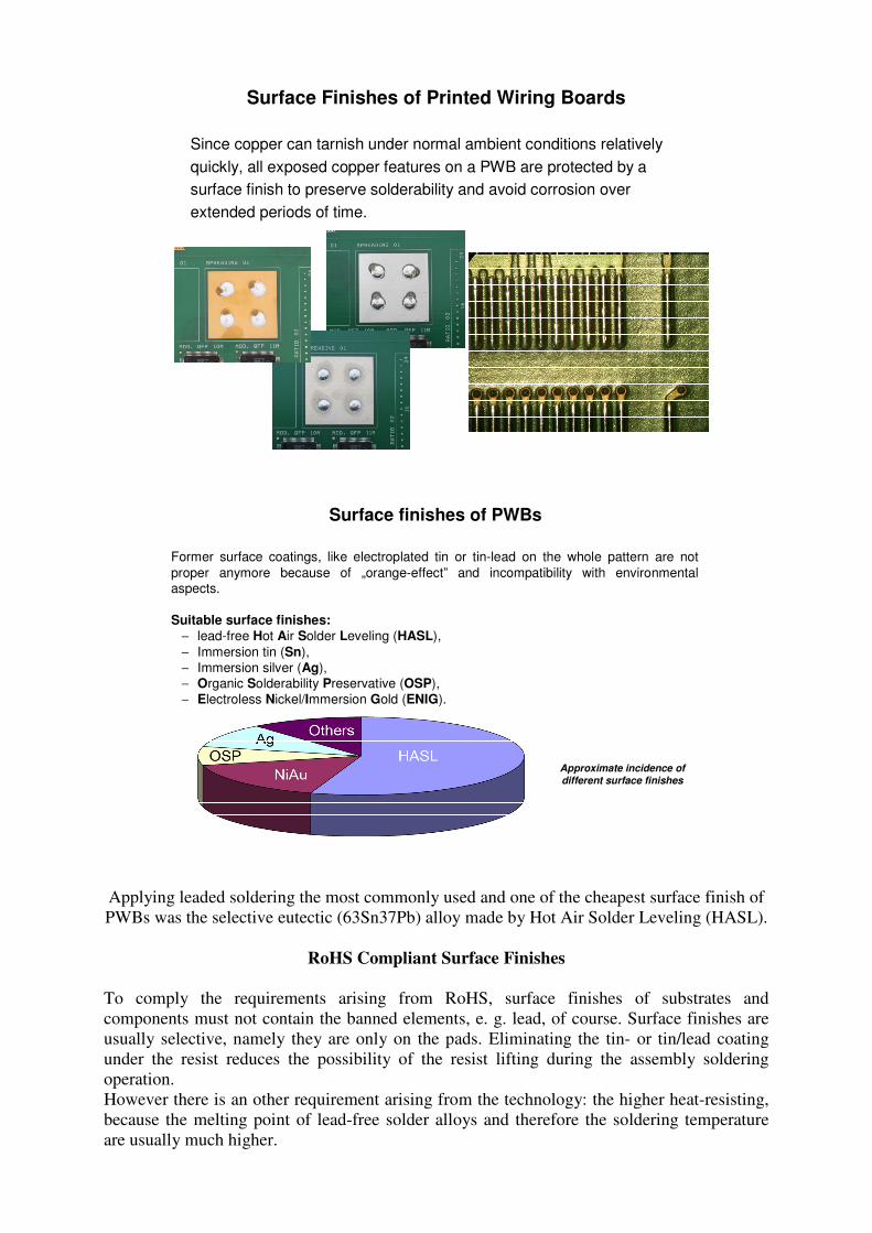
Surface Finishes of Printed Wiring Boards
Since copper can tarnish under normal ambient conditions relatively
quickly, all exposed copper features on a PWB are protected by a
surface finish to preserve solderability and avoid corrosion over
extended periods of time.
Former surface coatings, like electroplated tin or tin-lead on the whole pattern are not proper anymore because of „orange-effect” and incompatibility with environmental aspects.
Suitable surface finishes:− lead-free Hot Air Solder Leveling (HASL),− Immersion tin (Sn),− Immersion silver (Ag),− Organic Solderability Preservative (OSP),− Electroless Nickel/Immersion Gold (ENIG).
Surface finishes of PWBs
Approximate incidence ofdifferent surface finishes
Applying leaded soldering the most commonly used and one of the cheapest surface finish of
PWBs was the selective eutectic (63Sn37Pb) alloy made by Hot Air Solder Leveling (HASL).
RoHS Compliant Surface Finishes
To comply the requirements arising from RoHS, surface finishes of substrates and
components must not contain the banned elements, e. g. lead, of course. Surface finishes are
usually selective, namely they are only on the pads. Eliminating the tin- or tin/lead coating
under the resist reduces the possibility of the resist lifting during the assembly soldering
operation.
However there is an other requirement arising from the technology: the higher heat-resisting,
because the melting point of lead-free solder alloys and therefore the soldering temperature
are usually much higher.
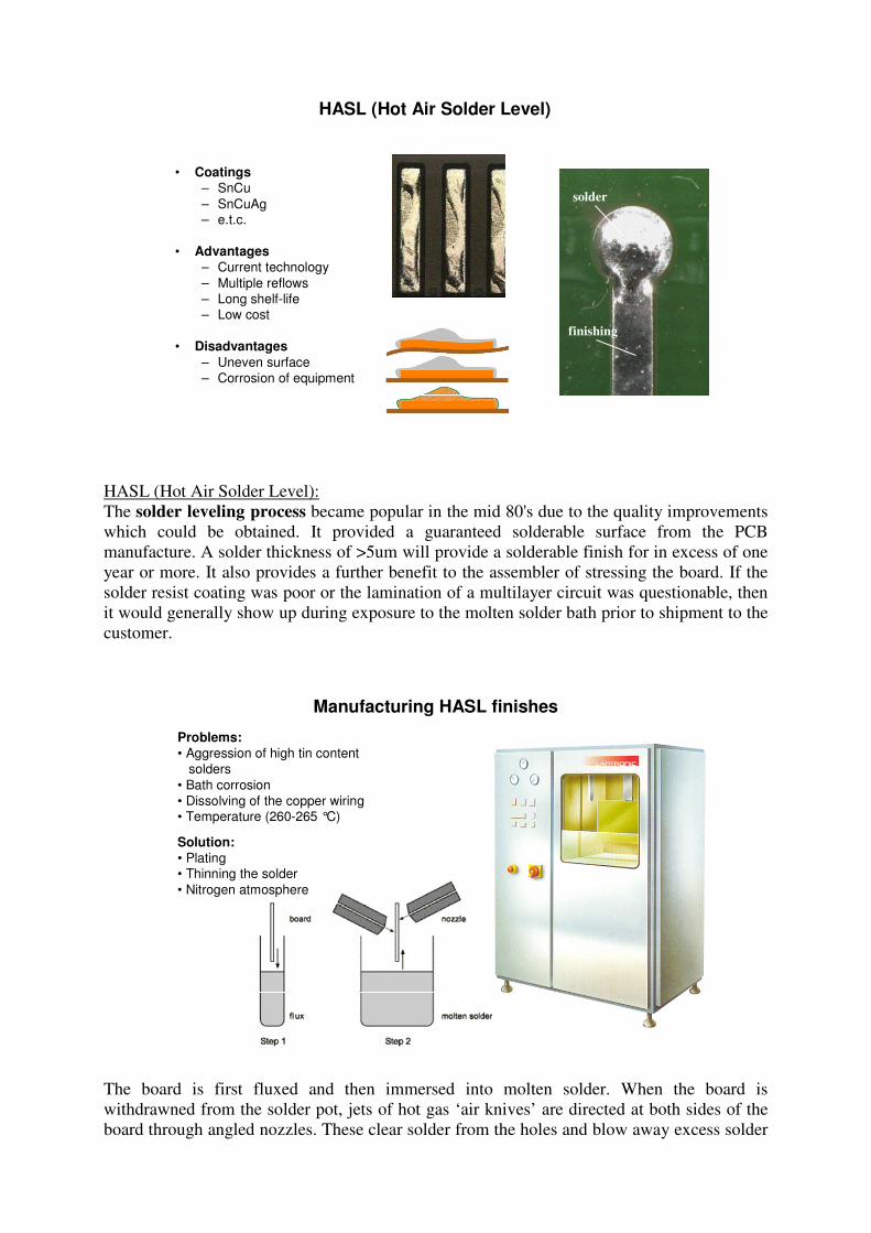
HASL (Hot Air Solder Level)
• Coatings– SnCu– SnCuAg– e.t.c.
• Advantages– Current technology– Multiple reflows– Long shelf-life– Low cost
• Disadvantages
– Uneven surface– Corrosion of equipment
solder
finishing
HASL (Hot Air Solder Level):
The solder leveling process became popular in the mid 80's due to the quality improvements
which could be obtained. It provided a guaranteed solderable surface from the PCB
manufacture. A solder thickness of >5um will provide a solderable finish for in excess of one
year or more. It also provides a further benefit to the assembler of stressing the board. If the
solder resist coating was poor or the lamination of a multilayer circuit was questionable, then
it would generally show up during exposure to the molten solder bath prior to shipment to the
customer.
Manufacturing HASL finishes
Problems:• Aggression of high tin content
solders• Bath corrosion• Dissolving of the copper wiring• Temperature (260-265 °C)
Solution:• Plating• Thinning the solder• Nitrogen atmosphere
The board is first fluxed and then immersed into molten solder. When the board is
withdrawned from the solder pot, jets of hot gas ‘air knives’ are directed at both sides of the
board through angled nozzles. These clear solder from the holes and blow away excess solder

from the pads, a process called as levelling. The temperature of the air used is usually at
around 240°C, a little lower than the solder bath.
The process can be carried out with the board held either vertically or horizontally: vertical
HASL gives better hole coverage and horizontal HASL gives flatter surface mount pads.
One of the problems with the vertical process is that one end of the panel receives a longer
dwell time than the other, resulting in differences in the growth of the intermetallic which
grows between tin and copper.
Immersion Sn
Whisker-formation
• Coating
– Sn
• Advantages
– Simple technology– Low price
• Disadvantages
– Danger of whisker-formation
– Limited shelf-life– Limited reflows
Sn2+ + 2Cu Sn + 2Cu+ solder
finishing
Immersion tin deposits 0.75 to 1.25 microns of tin utilizing an immersion plating process.
The tin deposit is modified by low levels of co-deposited organic and metallic additives. This
eliminates tin whiskers and limits the growth of tin-copper intermetallic. Immersion tin is the
thickest alternative coating to HASL and provides the best surface for compliant pins and In-
Circuit Test. The chemicals are delivered with superior performance and no-clean assembly
operations.

Immersion Ag
• Coating
– Ag
• Advantages
– Simple technology– Low price– Multiple reflows
• Disadvantages– Limited shelf-life (Must be
vacuumed packed for storage) – Chloride or sulfide atmosphere
causes tarnish
2Ag+ + Cu 2Ag + Cu2+
solder
finishing
Immersion Silver consists of a very thin coating of nearly pure silver. A slight amount of
organic material is typically deposited within the immersion silver intended to prevent tarnish
and electromigration. The metal coating is deposited via a relatively simple conveyorized or
vertical chemical process. Benefits of immersion silver include flatness, lead-free,
inspectability at assembly, lack of solder mask attack, and surface contact functionality.
Relative to other PCB coatings, immersion silver does not suffer from the black-pad
interfacial fracture phenomenon, tin-copper intermetallic shelf-life reduction, whisker
formation, or sensitivity to weak fluxes. Immersion silver plated on today’s clean, well
formed; well tested PCB’s is proven to be very functional in billions of solder joints in
existing electronics devices. For these reasons, OEM’s fabricators and assemblers have
increasingly used and specified immersion silver during the past 10 years.

Manufacturing Immersion Ag and Sn finishes
Laboratory equipment for immersion tin
CleaningCleaning
MicroetchingMicroetching
PreperationPreperation
Immersion processImmersion process
DryingDrying
Both Immersion Ag and Sn processes are easier to control, have short process times (high
throughput), and operate at moderate temperatures compared with ENIG. The coating
thickness depends on immersion time and coating bath temperature.
The typical process steps for immersion tin are the following:
1. Pre-cleaning: the acid cleaner removes oxides, organics and developer residues.
2. Microetching: on the copper to produce a highly active polished copper surface
3. Preparation: a conditioner creates an active copper surface on which the reaction can
take place. Prepares the surface for coating, and reduces the formation of oxide.
4. Immersion process carefully controlled to give a fine dense deposit of pure tin or
silver.
5. Drying: A warm-air drying stage, removes any residual moisture from the board.
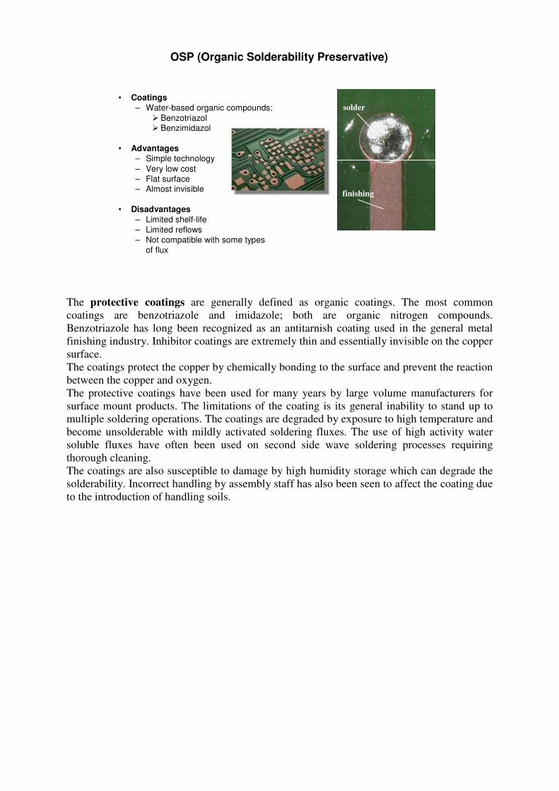
OSP (Organic Solderability Preservative)
• Coatings– Water-based organic compounds:
Benzotriazol Benzimidazol
• Advantages– Simple technology– Very low cost– Flat surface– Almost invisible
• Disadvantages
– Limited shelf-life– Limited reflows– Not compatible with some types
of flux
solder
finishing
The protective coatings are generally defined as organic coatings. The most common
coatings are benzotriazole and imidazole; both are organic nitrogen compounds.
Benzotriazole has long been recognized as an antitarnish coating used in the general metal
finishing industry. Inhibitor coatings are extremely thin and essentially invisible on the copper
surface.
The coatings protect the copper by chemically bonding to the surface and prevent the reaction
between the copper and oxygen.
The protective coatings have been used for many years by large volume manufacturers for
surface mount products. The limitations of the coating is its general inability to stand up to
multiple soldering operations. The coatings are degraded by exposure to high temperature and
become unsolderable with mildly activated soldering fluxes. The use of high activity water
soluble fluxes have often been used on second side wave soldering processes requiring
thorough cleaning.
The coatings are also susceptible to damage by high humidity storage which can degrade the
solderability. Incorrect handling by assembly staff has also been seen to affect the coating due
to the introduction of handling soils.

Manufacturing OSP finishes
Cleaning
Ide is kéne valami
animáció
MicroetchingMicroetching
Air knivesAir knives
Air knivesAir knives
DryingDrying
OSP applicationOSP application
The OSP process selectively applies a flat, anti-oxidation film onto the exposed copper
surfaces of the PWB to preserve the solderability of the copper.
1. Cleaning: the board must be cleaned by a series of cleaning chemicals. Each pre-
treatment chemical must be followed by water rinsing (normally two to three times) to
remove the chemical that adheres to the surface.
2. Microetching: on the copper to produce a highly active polished copper surface
3. Air knives: it removes the remaining water on the panel to limit oxidation formation
on the copper surfaces prior to coating application.
4. OSP application: the board is dipped in a solution of the OSP for 1–3 minutes. This
forms a chemical layer on the surface of the copper 2–10nm thick, depending on the
formulation.
5. Air knives: it removes the remaining OSP from the panel and promotes even coating
across the entire PWB surface.
6. Drying: A warm-air drying stage, removes any residual moisture from the board.

ENIG (Electroless Nickel/Immersion Gold)
• Coating
– Ni + Au
• Advantages
– Multiple reflows
– Long shelf-life
– Good Wettability
• Disadvantages
– More complicated technology than the Sn or Ag
– „Black pad” effect
– Expensive
solder
finishing
Gold is a traditional finish used in the electronics industry due to excellent electrical finish,
corrosion resistance and good solderability.
There has been some resistance to the use of gold due to concerns of reliability of the final
solder fillet. In the past, gold has been widely used for connectors; it was also used in the
1970's for a solderable coating on boards. The use of thick > 1µm gold coating lead to the
formation of gold/tin intermetalics which in turn lead to weak and fragile solder joints.
Ever since, soldering to gold has been avoided particularly in high reliability applications like
military and aerospace. Many existing standards relating to assembly and soldering require all
gold coatings to be removed prior to the final soldering operations.
Over the last ten years thin gold <0.25 µm over nickel have become popular finishes for
surface mount boards. They have provided an ideal assembly surface, highly solderable and
an aid to inspection due to the contrasting color between component leads and the solder paste.
Manufacturing ENIG finishes
MicroetchingMicroetching
Cleaning
CatalystCatalyst
Acid bathAcid bath
Electroless nickelElectroless nickel
Immersion goldImmersion gold
The gold coating does not oxidise, its excellent wettability by molten solder does not degrade
with time, and a plated finish maintains the flat surface of the copper lands. For these reasons

a gold finish fulfils the requirements for boards designed for fine-line printing. However, thin
gold plating is porous, and will not protect the underlying copper against oxidation. Oxidised
spots at the base of pores are a cause of dewetting, and copper can also diffuse to the gold
surface during heat treatments, where it can oxidise and thus impair wettability. To prevent
this, an electroless nickel underlayer is first deposited, to act as a barrier to copper diffusion:
1. Cleaning: the board must be cleaned by a series of cleaning chemicals. Each pre-
treatment chemical must be followed by water rinsing (normally two to three times) to
remove the chemical that adheres to the surface.
2. Microetching: on the copper to produce a highly active polished copper surface
3. Catalyst: The electroless nickel is an autocatalytic process that deposits nickel on the
palladium-catalysed copper surface.
4. Acid bath
5. Electroless nickel plating is an auto-catalytic reaction used to deposit a coating of
nickel on a substrate. Unlike electroplating, it is not necessary to pass an electric
current through the solution to form a deposit.
6. An overlay of gold to prevent corrosion.
E-test, ICT, keypad
noE-test, ICT,
keypadE-test, ICTE-test, ICTContact
80405070240…260Process temperature
(oC)
yesyesyesyesnoSmooth surface
30,70,80,81Relative price
24612618Shelf-life(months)
6262-36Number of reflow
cycles
4…6 +0,05…0,10
0,2…0,50,05…0,200,8…1,21…25Thickness (µm)
ENIGOSPAgSnHASLProperties
Comparing different surface finishes
Comparison of different surface finishes
HASL (Hot Air Solder Level) is the predominant final finish applied worldwide. HASL is a
predictable, well-known coating, it is used in billions of solder joints daily. However, the
uneven surface of lead-free HASL, which limits its application to fine pitch components, is
pushing the electronics industry to consider alternatives to HASL.
Numerous papers have been published over the last decade predicting the replacement of
HASL with organic solderability preservatives (OSPs), electroless nickel/ immersion gold
(ENIG) or new metallic immersion technologies such as silver and tin. So far, none of these
coatings has yet become so popular as HASL.
HASL alternatives allow a lead-free printed wiring board (PWB) and also provide flat
coplanar surfaces to meet technology demands. Finer pitch and area array devices have
allowed increased functionality of electronics. Typically, higher technology opposes lowering
cost. However, most alternatives improve high technology assembly and long term reliability
while still reducing cost.

Cost savings are the function of the entire process, i.e. costs that includes process chemistry,
labor and overhead. Alternatives like OSPs, immersion silver and immersion tin can provide a
20 to 30 percent reduction in final finishing costs. Although the percent saving per board may
be low in large high-layer count multilayer products, the cost savings with disposable
electronics, along with greater functionality and elimination of lead, will drive a dramatic
increase in the use of alternatives.
The use of alternatives would not only increase but would replace HASL as the final finish of
choice. ENIG, OSPs, immersion tin and immersion silver all provide lead-free, highly
solderable, coplanar surfaces that, under production conditions, provide significant
improvement in first pass assembly yields.
Failures on surface finishes
Black pad
(ENIG)
Whisker
(Imm. Sn)
Solder Mask Interface Attack
(Imm. Sn, Imm. Ag, ENIG)
The thickness of the copper decreases at the border of the solder mask
Dendrite
(Imm. Sn,
Imm. Ag, ENIG, HASL, OSP)
+ –
Solder Mask Interface Attack: The existing acid based aqueous processes contain toxic and
corrosive chemicals which degrade copper tracks. Corrosive chemicals in the ImAg process
get trapped under the soldermask edge and may erode the copper trace at the interface
between the solder mask and the copper trace.
Black Pad: Black pad forms during the immersion gold deposition step and it is a low-level
nickel corrosion defect. A compromised nickel surface and prolonged dwell in the immersion
gold bath is needed for its form. On an ENIG-finished board, the purpose of gold is to
preserve gold. If soldered properly, gold will dissolve and migrate into the solder ball, and
older will adhere to the nickel layer directly. Although if the nickel layer has small amounts of
contaminates that prevent good adhesion, gold dissolves, but the solder cannot mix and adhere
to the tin. This causes the black pad effect.
Whisker: The tin whisker is an electrically conductive single crystal structure of tin which
grows spontaneously. It has been observed of growing to lengths of several millimeters and
up to 5 µm in diameter. The mechanism of whisker growth had been studied for many years.
Although it is not well understood, it is thought that compressive mechanical stresses cause its
growth like residual stresses caused by electroplating, mechanically induced stresses; stresses
caused by diffusion of different metals, and thermally induced stresses. In the presence of
compressive stress, whiskers are extruded over time as a stress release mechanism.

Dendrite: Due to the electrochemical migration phenomenon. It develops when the circuit is
operating because it needs electrical voltage (DC) and a film of moisture. Metal ions are
formed due to anodic dissolving, they migrate through the electrolyte, and they exude on the
cathode in a dendrite form.
3. Surface finishes used on printed wiring boards
3.1 Surface Finishes of Printed Wiring Boards
Definition:– lead-free package is a standard package with lead removed from the lead finish coating or solder ball alloy.– lead-free package must be capable of withstanding reflow conditions with peak temperatures reaching 260 degree C.– lead-free package is part of Green package that is lead free, halogen free and high temperature capable.
There are a variety of surface finishes available for lead-free components leads, including:
- Tin (Sn), e.g. matte tin (100%Sn)- Tin Copper (SnCu) (e.g. Sn/0.7%Cu)- Nickel Palladium (NiPd), e.g. Ni-Pd/Au pre-plated lead frame- Palladium (Pd) - Tin Bismuth (SnBi) (e.g. Sn/2~3%Bi)- Tin Silver (SnAg) (e.g. Sn/3.5%Ag)- Tin Silver Copper (SnAgCu)
Market demands will determine the alternative finish of choice.
Lead-free Surface Coatings of Component Leads
Concerns regarding lead-free component coatings:
The change in surface finish materials from SnPb to alternative finishes has brought the
component supply chain under increased scrutiny. Despite having clear guidelines for labeling
components (IPC-1066 / JEDEC-97 Labeling Standard), suppliers have not demonstrated
consistency in identifying component finishes. In many cases the component manufacturer or
supplier cannot provide accurate information about the component surface finish. The
unknown surface finish issue is of particular concern for discrete components like chip
resistors and chip capacitors where part tracking can be more difficult.

The negative effects of surface finish uncertainty can be catastrophic. Materials interactions
can significantly reduce reliability. For example, a low temperature alloys is created when
bismuth interacts with SnPb, which can negatively affect product reliability. Additionally,
some surface finishes are sensitive to atmospheric conditions and require controlled
environments for both short and long term storage. These are some of the main reasons that
part tracking and inventory control have become secondary challenges associated with lead-
free conversions. However, whisker related risk is greater in high reliability electronics that
are used in harsh environments.
Recent studies showed that most manufacturers are producing lead-free components with a
matte tin finish. Component manufacturers cite the low cost of converting existing equipment,
compatibility with the current group of popular lead-free solders, and low risk of whisker
related failure in consumer products as the main reasons for producing tin finished
components.
The most popular lead-free finish is the matte tin despite industry concerns of tin whisker
formation. The problem of tin whiskers on component leads has been well documented. While
there is limited information on the exact growth mechanism, there are a number of mitigation
strategies available. These strategies range from simple processes such as annealing the tin
finish, to more complex processes such as plating underneath the tin finish with a stress
reducing under-plating.
Solderability of components and substrates means the wettability of their surface by molded solder. It can be characterized by the contact (wetting) angle as shown in the picture below:
Because the direct measurement of contact angle is difficult, there are different test methods in use for determination of solderability.
Contact angle – the measure of wettability
Non-wetting λ < 30°good wetting ideal wetting
A contact angle can be measured by dropping pure liquid on a solid. The angle formed
between the solid/liquid interface and the liquid/vapor interface and which has a vertex where
the three interfaces meet is referred to as at the contact angle.
The contact angle is described by the Young-Dupre equation, where:
γgs = surface tension of the gas-solid boundary,
γls = surface tension of the liquid-solid boundary,
γlg = surface tension of the gas-liquid boundary,
θ = contact angle.

The most common used solderability test methods are as follows:
- wetting balance test,
- bridging test,
- spreading test.
They are suitable for comparison and/or optimization of different solder alloys,
fluxes, surface finishes, technological parameters of soldering etc.
However the results of tests performed with different methods mostly are not comparable.
Solderability test methods
Steps and the resulting diagram of Wetting Balance Test
a) sample before dipping;b) right after dipping, the surface-tension
works against the dipping;c) the surface-tension is equal to zero, only
the buoyancy affects the sample;d) after wetting the surface-tension works
against the lifting;e) lifting of sample;f) lifted sample.
Wetting Balance Test
A quantitative method for determining the solderability is the Wetting Balance Test method.
This method measures the time for the solder to wet the component termination or pad. Two
important attributes of the wetting balance curve are the time to 2/3 of maximum force (t2/3)
and maximum force (Fmax).
In the conventional wetting balance test the leaded components after fluxing are immersed in
a bath of molten solder and the time taken to wet the leads and the wetting force is measured
and a wetting balance curve produced.
However for specimens having small wettable areas such as chip resistors, chip capacitors,
pads etc., a globule of molten solder is substituted for the solder bath. The specimens are

tested using zero immersion depth; this method has so far shown to produce reproducible
results.
no wetting poor wetting good wetting delayed wetting
de-wettingirregular wettingfast wettingslow wetting
Click on the figure to start movie!
Performance of theWetting Balance Test
Wetting Balance Test
0,1 µN
ms
Example Test Coupon Prior to Reflow
Modest solderability
Excellent solderability
Direction of dot count
Bridging test coupons after stencil printing and reflow process
Bridging Test
Using permanent wetting test patterns can be simple and eliminate the need for costly test
equipment. It is easy to build up a library of data which can be compared with changes in
production profiles, new pastes and other process changes. The test method can be used to
compare the degree of wetting between different alloys.
By simply adding a group of parallel lines on panel areas of a circuit board or on an open area
of a board, testing can be conducted on every board produced. It is also possible to select
sample boards at goods receipt, if required to check solderability using a true production
environment and the intended combination of materials. In this case the paste is printed only
on the test pattern of 72 dots using a mini stencil prior to running a board through reflow.
Each time a panel is printed with solder paste the test coupon is also printed. Solder paste dots
are printed along the parallel tracks with decreased spacing between the dots. During reflow
and depending on the solderability of the surface finish, paste
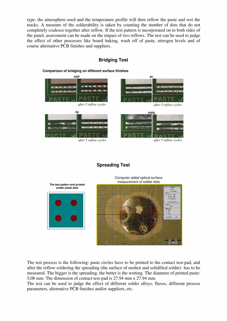
type, the atmosphere used and the temperature profile will then reflow the paste and wet the
tracks. A measure of the solderability is taken by counting the number of dots that do not
completely coalesce together after reflow. If the test pattern is incorporated on to both sides of
the panel, assessment can be made on the impact of two reflows. The test can be used to judge
the effect of other processes like board baking, wash off of paste, nitrogen levels and of
course alternative PCB finishes and suppliers.
Comparison of bridging on different surface finishes
Bridging Test
OSP
after 5 reflow cycles
Ag
after 5 reflow cycles
Sn
after 5 reflow cycles
HASL
after 5 reflow cycles
Computer aided optical surface measurement of solder dots
Spreading Test
The test pattern and printed solder paste dots
The test process is the following: paste circles have to be printed to the contact test-pad, and
after the reflow soldering the spreading (the surface of molten and solidified solder) has to be
measured. The bigger is the spreading, the better is the wetting. The diameter of printed paste:
5,08 mm. The dimension of contact test-pad is 27.94 mm x 27.94 mm.
The test can be used to judge the effect of different solder alloys, fluxes, different process
parameters, alternative PCB finishes and/or suppliers, etc.

4. Solder paste stencil printing4.1 Stencil manufacturing technologies
Solder paste deposition
The solder paste can be applied in two ways to the pads; by dispensing or by stencil printing. Due to its productivity stencil printing is the method for mass applying solder paste, where a squeegee forces the paste through the apertures to pads in one step. Dispensing is slower process because the paste is applied to pads one by one, therefore this method is used mainly at prototyping. Its advantage is that a relatively expensive stencil is unnecessary.
Dispensing solder paste Stencil printing process
The solder paste can be applied in two ways to the pads; by dispensing or by stencil printing.
Due to its productivity stencil printing is the method for mass applying solder paste, where a
squeegee forces the paste through the apertures to pads in one step. Dispensing is slower
process because the paste is applied to pads one by one, therefore this method is used mainly
at prototyping. Its advantage is that a relatively expensive stencil is unnecessary.

Stencil manufacturing methods include three technologies; chemical
etching, laser cutting and electroforming. All technologies have advantages and disadvantages, which should be taken into accountwhen choosing stencil for given application.Chemical etching
- Subtractive technology, cheap- Hour-glass shape aperture, material: brass- Appropriate for pitch size: >0.063 mm
Stencil Manufacturing Technologies – chemical etching
Cross-section of chemical etched stencil aperture
Chemical etched stencils are the workhorses of the stencil world. They are the most cost
effective and the quickest to turn around. (Same day shipments are a daily occurrence.)
Chemical etched stencils are created by coating a metal foil with resist, exposing an image
onto both sides with a pin-registered photo tool and then etching the foil from both sides
simultaneously using a dual-sided process. Since the process is dual-sided, the apertures, or
openings, are created as the etchant works through the metal not only from the top and bottom,
but also horizontally. Inherent in this technique is the creation of a knife edge, or hourglass,
configuration. While at 0.5 mm pitch and under, such a profile presents an opportunity for
paste adherence into apertures.
Chemically cleaned surface
Photo sensitive coating applied to both top and
bottom
Developing solved photo-resist
Etching of metal Complete etched product
Rinsing off photo-resist
Chemical Etched Stencils

The steps of chemical etching are the followings:
1. Chemically clean the surface of the metal to be etched
2. Apply photo sensitive coating to both top and bottom sides
3. Develop the photo resist usually by UV light
4. Rinse off the photo resist
5. Etch the metal from both sides
Stencil Manufacturing Technologies - lasercutting
Laser cutting- Subtractive technology, medium price- Trapezoidal aperture, material: nickel or stainless steel- Appropriate for pitch size: >0.4 mm
Cross-section of lasercut stencil aperture
Lasercutting stencil foil
Produced directly from the customer's original Gerber data, laser-cut stainless-steel
stencils feature an absence of photographic steps. Hence, eliminating the opportunity for
mis-registration. A stencil can be made with excellent positional accuracy and
reproducibility The Gerber file, after the necessary modifications, is transferred to (and
directly drives) the laser. Less physical intervention means fewer opportunities for error.
Although there were initial concerns about the dross (vaporized molten metal) created by
the laser beam, the current generation of laser cutters produces minimal dross that is
removed easily. The major drawback of the laser-cut process is that the machine cuts each
aperture individually. Naturally, the more apertures, the longer it takes and the more
costly the stencil. The laser technique is the only process that permits an existing stencil to
be reworked, e.g., to add apertures, enlarge existing apertures or add fiducials.

A trapezoidal aperture may be used to enhance solder paste
release. In chemical etch processes, the trapezoidal dimension, Z, can be specified. At lasercut process trapezoidal apertures are created automatically per the laser beam's focus, which aids paste release. The aperture openings actually are cut from the contact side of the stencil, the stencil then is flipped and mounted with thesqueegee side up.
Trapezoidal Apertures
A trapezoidal aperture may be used to enhance solder paste release. In chemical etch
processes, the trapezoidal dimension, Z, can be specified. At lasercut process trapezoidal
apertures are created automatically per the laser beam's focus, which aids paste release.
The aperture openings actually are cut from the contact side of the stencil, the stencil then
is flipped and mounted with the squeegee side up.
Stencil Manufacturing Technologies - electroforming
Electroforming- Additive technology, expensive, - Material: nickel- Appropriate for pitch size up to: 0.2 mm
Cross-section of electroformed stencil aperture
Electroforming creates a nickel stencil with a unique gasketing feature that reduces
solder bridging and minimizes the need for underside stencil cleaning. This process
provides near-perfect registration with no geometric limitations, smooth vertical side-
walls with a built-in taper and low surface tension to enhance paste release. The stencil is
created by imaging photoresist on a substrate where the apertures are intended and then
plating - atom by atom, layer by layer - the stencil around the resist to the desired
thickness. During the process the nickel atoms are deflected by the photoresist to create a

trapezoidal configuration. Next, when the stencil is removed from the substrate, the top
becomes the contact side to create the gasketing effect. A continuous nickel thickness
range of 25 to 300 µm may be selected. This process is ideally suited for ultra-fine-pitch
requirements (0.2 to 0.4 mm). As for drawbacks, since a phototool is involved (albeit one-
sided) the potential for misregistration exists. And if the plating process is not uniform,
the gasketing effect is negated.
Metal substrate, cleaned and degreased
Electro deposition of metal
Separation of stencil Complete stencil
Developing and rinsing off solved photo-resist
Photo-sensitive coating applied
Electroformed Stencils
The steps of electroforming are the followings:
1. Clean the metal substrate,which is usually nickle
2. Apply photo resist
3. Develop and rinse off the photo resist
4. Deposit metal by galvanizing around the photo resist
5. Remove photo resist and separate the stencil foil from the substrate

4. Solder paste stencil printing4.2 Properties of solder pastes
Solder paste is a combination of pre-alloyed spherical metal powder and
flux medium.
Properties of Solder Pastes
Solder paste Packing of solder pastes: jar and syringe
Solder paste
http://engweb.gre.ac.uk/emerg/images/solder%
20paste%20particles.jpg
© Senju
Solder paste is a combination of pre-alloyed spherical metal powder and flux medium.
Solder paste formulations are designed with specific characteristics of tack time, stencil
life, and rheology (flow characteristics). As solder paste ages and is used in production,
these characteristics will change. Handling solder paste properly will preserve the original
characteristics of the solder paste longer, resulting in less paste waste, better process yield,
and lower defect rates.

Properties of Solder Pastes
Freshly opened solder paste Excessive heat damaged solder paste
Preparing solder paste - stirring Applying solder paste to stencil
© Bob Willis © Bob Willis
© Bob Willis© Bob Willis
Moisture Moisture is a contaminant, and is perhaps the most detrimental element that solder paste
can be exposed to. Moisture can cause and increase powder oxidation, which in turn
requires more of the activator to expend itself on cleaning the solder powder and less for
cleaning the components and substrate. This may result in poor or non-wetting. Moisture
also causes slumping that can lead to bridging, may result in solder balling when the paste
is reflowed, can result in flux/solder spatter, and can reduce tack time.
Solder Paste Storage It is critical that solder paste be received in and stored as soon as it arrives to its final
destination. Solder paste should not remain on the receiving dock where it could be
exposed to excessive heat, humidity, or cold. It is generally recommended to store solder
paste in refrigeration at 40°F/4°C Excessive Heat Because solder paste is made of two ingredients with very different densities, it is normal
in some formulations for a bit of flux to separate out of the paste and rise to the top of the
material. If a solder paste is exposed to excessive heat for a prolonged period of time,
however, the separation of the flux medium from the body of the paste may increase
dramatically. This is recognizable when opening a jar of solder paste or viewing the
contents of a container; although it is natural and acceptable for some flux to appear on
the surface of the solder paste, if the paste has become heat damaged a thick deposit of
flux will be floating on top of the paste.
Printer Area Conditions As stated earlier, heat and humidity are damaging to solder paste. Ideally, the printing area
should be maintained at 40% - 50% relative humidity and 72°- 80°F (22-26°C). In
addition, no air (cool or warm) should blow directly on the top or bottom of the stencil, as
this can cause paste dry-out.
Preparing Solder Paste: Warming Before solder paste is used, it should be removed from refrigeration and allowed to warm
naturally to ambient temperature. Do not remove any seal, open, or attempt to mix solder

paste until it has warmed completely to room temperature. The typical warming or
stabilization time for solder paste is four to six hours. Do not force warm solder paste, as
this may cause flux separation and/or rheological problems.
Preparing Solder Paste: Stirring Once it has warmed adequately, mix the solder paste lightly and thoroughly in one
direction for one to three minutes by a means of spatula. This will ensure an even
distribution of any separated material throughout the paste. However, care should be taken
not to over-mix the solder paste by stirring it too vigorously or for too long. This can
result in overly shear-thinning the solder paste, which can result in slumping and/or
bridging. Applying Solder Paste to the Stencil The initial application of solder paste onto the stencil typically is two to three times
greater than applications made during the print cycle. The initial bead of solder paste
should be the full length of the printable pattern on the stencil, in a diameter of
approximately 1/2 to 5/8 inch. Controlling the level of solder paste on the stencil surface
is vital to proper printing. It is better to add a smaller amount of paste more frequently
than to add a large amount of paste less often. This method of control will ensure a more
frequent turnover of paste, keeping it fresh.
Storing Opened Solder Paste Containers Once a jar or cartridge has been opened it should not be re-refrigerated. If solder paste
remains in a container that has been opened, simply re-seal the jar or cartridge and leave it
out at room temperature until it is ready to be used again. Re-refrigerating the paste can
cause any moisture that has been absorbed into the paste to condense, which can then
result in the aforementioned moisture-related problems.
4. Solder paste stencil printing4.3 Parameters of stencil printing process
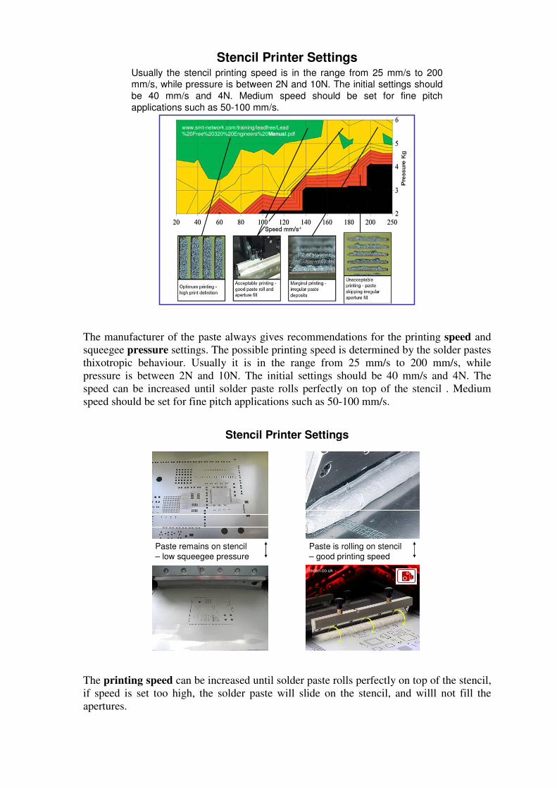
Usually the stencil printing speed is in the range from 25 mm/s to 200mm/s, while pressure is between 2N and 10N. The initial settings should be 40 mm/s and 4N. Medium speed should be set for fine pitch applications such as 50-100 mm/s.
Stencil Printer Settings
www.smt-network.com/training/leadfree/Lead%20Free%20320%20Engineers%20Manual.pdf
The manufacturer of the paste always gives recommendations for the printing speed and
squeegee pressure settings. The possible printing speed is determined by the solder pastes
thixotropic behaviour. Usually it is in the range from 25 mm/s to 200 mm/s, while
pressure is between 2N and 10N. The initial settings should be 40 mm/s and 4N. The
speed can be increased until solder paste rolls perfectly on top of the stencil . Medium
speed should be set for fine pitch applications such as 50-100 mm/s.
Stencil Printer Settings
Paste is rolling on stencil – good printing speed
Paste remains on stencil – low squeegee pressure
tecan.co.uk
The printing speed can be increased until solder paste rolls perfectly on top of the stencil,
if speed is set too high, the solder paste will slide on the stencil, and willl not fill the
apertures.

The squeegee pressure should be as low as possible because too much pressure abrades
the stencil. Pressure should be increased only when paste remains on stencil after printing,
the squeegee does not wipe the stencil thoroughly. If adjusted correctly, a thin layer of
flux will remain on top of the stencil and paste is rolling in front of the squeegee. The
amount of pressure is determined by printing speed and stencil type.
The squeegee down stop is a mechanical stop that prevents the squeegees to move further
down. It must be adjusted only to just touch the stencil surface. However, if the squeegee
axis and the stencil are not perfect parallel it can be necessary to over-adjust the down
stop to compensate. But, if the down stop is adjusted too far down, both stencils and
squeegees will wear out rapidly. Some machines do not have a mechanical down stop but
a squeegee origin point. Usually were the squeegee just touches the stencil.
The snap off speed of, which means the speed of separation between stencil and PWB
after printing is important. A too rapid separation speed when printing fine pitch will
result in clogging of the stencil apertures. A too fast or slow separation will also result in
tailing and form high edges around the solder paste deposits. The ideal separation speed
depends on the solder paste and the stencil aperture wall smoothness. On the other hand, a
slow separation speeds will slows down the printing cycle time.
4. Solder paste stencil printing4.4 Troubleshooting of printing failures

The assembly line and defect rates for proces steps
Conventional stencil printing is increasingly being proposed as a cost
effective process solution for applying solder paste for electronic components that appear to be continuously shrinking in scale. This is particularly true in the SMT industry where the solder paste deposition operation is already recognized as a major contributor to end-of-line defects. Therefore the process of depositing solder paste on a circuit board is critical to the success of fine feature assembly.
In the surface mount assembly, the stencil-printing method is used to deposit the solder
paste onto the printed circuit boards (PCBs). The need for higher pin count, higher
performance, smaller size, and lighter weight has driven the development of fine pitch and
ultra-fine stencil-printing applications. Many surface mount assembly manufacturers
encounter significant trouble-shooting time associated with problems of solder-paste
printing quality, and this can be as high as 40% of production time. The stencil-printing
stage is the most critical step of the surface mount assembly process. Industry reports have
shown that about 60% of soldering defects for the end products are related to the solder-
paste printing. The earlier a defect is detected in the assembly process, the less expensive
are the fixing costs required to compensate for it. Repair and rework costs vary. However,
usually, a 5 to 10-fold increase in cost occurs after each successive production step.
Accordingly, the quality of solder-paste printing is one of the key factors by which a
manufacturing firm can gain a competitive edge.
The objective of a stencil-printing process is to transfer the solder paste into the stencil
aperture by the action of squeegee, leaving a desired amount of solder paste on the pads of
the substrate. The deposited height, area, and volume are the determinant factors of
printing quality.

Paste bleeding under stencil – can lead to bridging
- Increase frequency of under stencil cleaning
- Check the gasketing- Check board height- Check board support- Check print pressure
Paste build up under stencil – one side of the aperture has
paste build up
- Increase frequency of under stencil cleaning
- Check the gasketing
Troubleshooting Printing Failures
The paste bleeding under the stencil can lead to solder bridging after soldering, which
cause electrical short between two or more adjacent component leads. The bleeding can be
prevented by increasing the frequency of under stencil cleaning, and gasketting (gap
between the board and the stencil) should be zero. The proper settings for board height,
board support and print pressure should be checked as well.
The paste buildup on one side of the stencil can be prevented by the before mentioned
methods too.
Troubleshooting Printing Failures
- Check the paste roll, drop-off and abandon time
- Check the mass of paste on stencil- Check the cleanliness of apertures
Incomplete transfer of paste from stencil onto pads
- Increase squeegee pressure- Check separation speed- Check gasketing- Check board support- Check stencil thickness
Too much paste has been deposited onto board – can lead to bridging
Incomplete paste transfer onto the board can lead to open joints (i.e. there is no joint
between the board and the component lead). In the case of this failure the mass of paste on

stencil, the cleanliness of apertures the printing speed (proper rolling of paste during
printing) and paste abandon time should be checked.
When too much paste is transfered onto the board (which can lead to bridging) the
squeegee pressure should be increased, and gasketing, board support and stencil thickness
should be checked.
Poor print definition “Dog-ears” – can cause solder bridges during reflow
- Check separation speed- Check tackiness of paste- Check stencil thickness- Increase print speed and check PWB
support
Paste scooping – insufficient paste on pads, concave profile
- Make sure the pressure isn’t too high- Ensure that metal blades are being used- Check also the blade edge- Check stencil is ‘on contact with PWB
Troubleshooting Printing Failures
Poor print definition can be prevented by increasing printing speed. Stencil separation
speed, tackiness of paste and board support should be checked as well to prevent this
failure.
Paste scooping (which can lead to open joints) usually caused by too high squeegee
pressure. Although the edge of the printing blade and board support should be checkek
also.
Troubleshooting Printing Failures
- Reduce print pressure- Check the gasketing- Check the understencil cleanliness- Make sure that multiple prints haven’t occurred- Make sure that the board is handled correctly
Paste bridging and smearing. Bridging has occurred
- Board has been handled incorrectly during assembly- Review board handling and storage after printing
Paste deposit partially removed after printing
Paste bridging and smearing can be prevented by reducing squeegee pressure. In addition
the gasketing and understencil cleanliness should be checked.
If the deposited paste partially removed during stencil separation, the cleanliness of the
board should be checked. Usually board contamination is the cause of this failure.

Smudged print. Paste deposits have bad edgedefinition
- Check handling procedures to ensure paste deposits are not disturbed after printing
Paste is rolling in front of squeegee blade
- Ideal printing conditions
Troubleshooting Printing Failures
Smudge prints are usually caused by human mistakes, when the operator disturbs the
deposited paste accidentally after printing.
The ideal printing conditions are the followings:
1. The paste is rolling on the stencil
2. The squeegee moves smoothly, applying even pressure along the full length of
blades
3. The squeegee cleans the stencil, i.e. no paste remains after printing on stencil at
the printing area.
Troubleshooting Printing Failures
- Check stencil geometry possibly reduce aperture: pad ratio
- Check ambient conditions – excessive heat or humidity
- Check squeegee settings- Check paste abandon time- Check stencil is ‘on contact’
Paste has slumped after printing process has been completed
- Ideal paste deposit
Brick shaped deposit
The slumping of paste usually caused by improper ambient conditions, by excessive heat
or moisture. The paste abandon time on stencil and after printing should be checked and
controlled.
The ideally deposited paste has brick shape with sharp and definite edges.

4. Solder paste stencil printing4.5 Stencil life and care
Cleaning stencils
Stencil should be cleaned thoroughly before and after manufacturing as well. The cleaning solvent can be isopropyl alcohol or solvents recommended by the manufacturer of the paste or stencil.
Contaminated stencil Clean stencil
The stencil is the prime element in determining the application of the exact amount of
material in the exact location. Therefore it is important that a stencil is considered as a
precision engineered tool that is vital to the overall process performance and should be
cared for as such. Most stencils will not be used to the end of their stencil life due to:
- Design Revision (layout change)
- Process Optimization (corrective action)
- Damage (handling)
- Wear (use)
Even so monitoring stencil life is critical to the overall print process performance and
consistency.
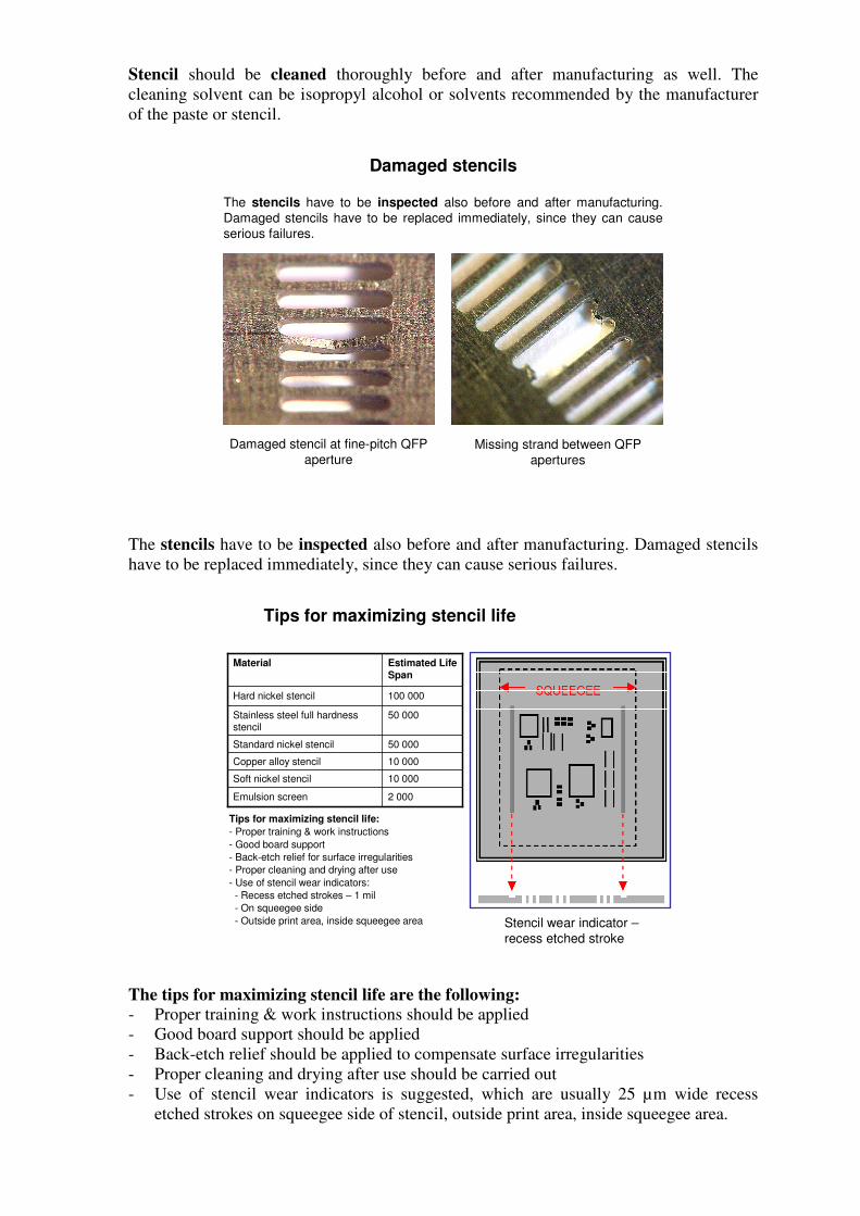
Stencil should be cleaned thoroughly before and after manufacturing as well. The
cleaning solvent can be isopropyl alcohol or solvents recommended by the manufacturer
of the paste or stencil.
The stencils have to be inspected also before and after manufacturing. Damaged stencils have to be replaced immediately, since they can cause serious failures.
Missing strand between QFP apertures
Damaged stencil at fine-pitch QFP aperture
Damaged stencils
The stencils have to be inspected also before and after manufacturing. Damaged stencils
have to be replaced immediately, since they can cause serious failures.
Tips for maximizing stencil life:
- Proper training & work instructions
- Good board support
- Back-etch relief for surface irregularities
- Proper cleaning and drying after use
- Use of stencil wear indicators:
- Recess etched strokes – 1 mil
- On squeegee side
- Outside print area, inside squeegee area
2 000Emulsion screen
10 000Soft nickel stencil
10 000Copper alloy stencil
50 000Standard nickel stencil
50 000Stainless steel full hardness stencil
100 000Hard nickel stencil
Estimated Life Span
Material
Tips for maximizing stencil life
Stencil wear indicator –recess etched stroke
The tips for maximizing stencil life are the following: - Proper training & work instructions should be applied
- Good board support should be applied
- Back-etch relief should be applied to compensate surface irregularities
- Proper cleaning and drying after use should be carried out
- Use of stencil wear indicators is suggested, which are usually 25 µm wide recess
etched strokes on squeegee side of stencil, outside print area, inside squeegee area.

5. Component placement
Component placement machines
Placement machines are supposed to place the electronic components into the
deposited solder paste.
They can be grouped by:
- the degree of automatization:
manual, semi-automatic, automatic
- by the mechanism of actuation:
Gantry style, walking beam style
- by the design of placement head
pick and place, collect and place

Manual placement machines
Manual placement machines are ideal for laboratories and small volumes, if theproduct changeover frequent.
The speed of manual placement machines is around 100 components per hour.
Semi-automatic placement machines
Semi-automatic placement machines place the components automatically. Onlythe transportation of the PCB into the machines, and into the reflow oven afterplacement, is carried out manually by the operator.
The speed of the semi-automatic placementmachines is approxima-tely 3.000 – 6.000 components per hour.

Automatic placement machines
Automatic insertion machines make it possible to insert many through-hole components into the holes of a circuit board, or place lots of surface mount components onto the printed wiring board in a very short time.The speed of automatic placement machines is up to 100.000 components per hour for passive components. The speed of 15.000 components per hour is common for fine-pitch IC packages.
Mechanism of actuation – walking beam style
Walking-beam machines. The walking-beam-style machine is designed for extremely high-volume production environments. PCBs usually are mounted on a pallet just prior to assembly and then the pallet is indexed step-by-step through a number of placement stations. This style machine is extremely popular with a very small, but highly respected market segment. Although the design is very efficient, it is not very friendly when changing from one product to another.
To change to a different product, the pallets must be adjusted, the feeders repositioned and the heads retooled, limiting popularity to products requiring nonstop production of a limited number of products.

Mechanism of actuation – gantry style
Gantry-style machines use a placement head mounted on a beam, allowing the placement head access to all the feeder positions as well as the circuit board. The component feeders and the PCB all remain stationary in this design, and the pick-up head mounted on the gantry goes to the feeders, gathers the components, image processes the parts and then delivers them to the correct placement point on the circuit board.
To increase speed, gantry-style machines often have many nozzles on a single head and may use more than one gantry per machine, in sort of a "tag team" approach. As one head is collecting parts, the other is placing parts, and vice versa.
Placement heads - pick and place
Pick and place machines pick and place components one by one. The efficiency of these machines is up to 20.000 components per hour. The accuracy of these machines is relatively high (10-20 µm), therefore fine-pitch IC packages are always placed with pick and place heads.
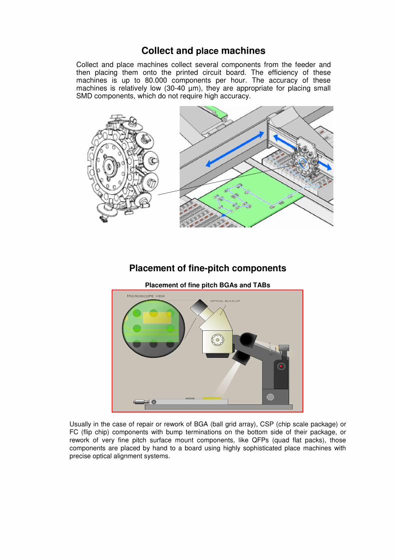
Collect and place machines
Collect and place machines collect several components from the feeder and then placing them onto the printed circuit board. The efficiency of these machines is up to 80.000 components per hour. The accuracy of these machines is relatively low (30-40 µm), they are appropriate for placing small SMD components, which do not require high accuracy.
Placement of fine-pitch components
Placement of fine pitch BGAs and TABs
Usually in the case of repair or rework of BGA (ball grid array), CSP (chip scale package) or FC (flip chip) components with bump terminations on the bottom side of their package, or rework of very fine pitch surface mount components, like QFPs (quad flat packs), thosecomponents are placed by hand to a board using highly sophisticated place machines with precise optical alignment systems.

Component placement failures
- Component falls down from the nozzle
- Misplacement, and rotational offset of the placed
component
- Wrong polarity
- Billboard
6. Reflow soldering
Soldering and heat transport methods
Soldering is the process in which two metals are joined together by means of a third metal or alloy having a lower melting point.
Soft soldering is characterized by the value of the melting point of the third metal or alloy, which is below 400 °C. The third metal or alloy used in the
process is called solder.
We need heat transport:
- to melt the solder
- to heat up the soldered samples
- to activate the flux

Infra Radiation (IR) occurs when two bodies of different temperatures are in sight of
each other.
The heat is transferred by electromagnetic waves of 0.78 to 1000 micron wavelengths. All
objects emit some level of infrared energy. Fluxes, plastic components, and epoxy glass
laminate absorb IR very well. Shiny surfaces will reflect the IR energy away.
Conduction heat transport occurs when two solid masses on different temperatures are in
contact with each other. Conduction heat will penetrate from the hotter solid to the cooler
solid. The most important thing in this heat transfer method that the solids most be in
contact.
Convection heat transfer occurs when a fluid (gas or liquid) passes over an object.
Temperature differences between the fluid and the objective create the convective heat
transfer. Convection heating or cooling requires contact of the flow with the solid part.
Convection may be classified as natural or forced. Natural convection occurs when no
flow is being forced over the object. Forced convection requires an external force that
pushes or pulls the flow over the object. The forced convection heating or cooling rates
are higher than natural convection rates.
Terms of soldering
Thermal profile: „the way of the
heating” means the temperature
changes in the function of time
∆T: the highest temperature difference between different locations of the assembly in the same moment during the
soldering.
Process Window:a temperature interval where the peak temperature should be existed during the soldering
Infra Radiation (IR) occurs when two bodies of different temperatures are in sight of
each other. The heat is transferred by electromagnetic waves of 0.78 to 1000 micron
wavelengths. All objects emit some level of infrared energy. Fluxes, plastic components,
and epoxy glass laminate absorb IR very well. Shiny surfaces will reflect the IR energy
away.
Conduction heat transport occurs when two solid masses on different temperatures are in
contact with each other. Conduction heat will penetrate from the hotter solid to the cooler
solid. The most mportant thing in this heat transfer method that the solids most be in
contact.
Convection heat transfer occurs when a fluid (gas or liquid) passes over an object.
Temperature differences between the fluid and the objective create the convective heat
transfer. Convection heating or cooling requires contact of the flow with the solid part.
Convection may be classified as natural or forced. Natural convection occurs when no
flow is being forced over the object. Forced convection requires an external force that

pushes or pulls the flow over the object. The forced convection heating or cooling rates
are higher than natural convection rates.
Terms of soldering
Wetting: means the spreading of themelted solder on the contact surfaces.Suitable wetting needs to the jointformation.
Solder
Soldering surface
Thermal profile
The profile can be broken down into five zones: pre-heat, pre-flow or soak, rump-up,
reflow, and cool down.
During the pre-heat phase, the solvents evaporate from the solder paste. If the
temperature rises too rapidly during the pre-heat, two problems can occur. First, solder
balls can be spread when the solvents burst through the flux surface membrane. This is

called solder balling. Second, the solder paste can slump, because too rapid a temperature
rise changes the viscosity of the solder paste. This will result in bridging. A typical
preheat phase has a slope of 0.5…1.0 °C/s.
The pre-flow or soak and the rump-up section, also called the flux activation stage, brings
the entire assembly device up to the temperature at which the paste changes from solid to
liquid, and becomes active. This soak time should be long enough to allow the flux to
clean the bonding surfaces, but not so long that the flux is evaporated prematurely.
During the reflow phase, the temperature increases to melt the solder paste alloy and
subsequently the solder and the copper begin the formation of intermetallic solder joints.
The typical solder temperature is 30…40 °C above the solder paste melting point.
In the cool down phase, a reliable solder joint is formed. For a strong bond between the
pad and the terminal, the cooling should be fast.
After suitable pre-heat, soak and rump-up sections, during the reflow phase, the
temperature increases to melt the solder paste alloy and subsequently the solder and the
copper begin the formation of intermetallic solder joints. The typical solder temperature is
30…40 °C above the solder paste melting point. It is important to monitor the time at peak
reflow temperature in several areas of the PCB.
The cool down phase is a critical step in the formation of a reliable solder joint. For the
solder joint to perform as a strong bond between the solder pad and the component
terminal, the cooling should be as fast as possible. A slower rate may increase the grain
size of the intermetallic compounds making the solder joint brittle and weak. On the other
hand, the components can crack if the temperature drops too rapidly. The cooling should
therefore be 3…4 °C/s down to around 130 °C. Below 130 °C the cooling rate is not
critical to the solder joint quality, however fast cooling is beneficial for copper OSP board
rather than a very slow cooling rate. The solderability will be maintained for second side
reflow, wave or selective soldering.
Conveyor speed is a critical component of the reflow profile speeding up or slowing the
conveyor results in altered temperature profiles.

Thermal profile
Reflow profiles
The applied reflow profile (soak or linear) dependent on the size and complexityof the circuit board.

Reflow ovens
Batch reflow ovens:• mainly applied IR heating• only 1 heating zone• small size• off-line machines• low capacity• for small series• for simple assemblies
Reflow ovens
IR heating + convectional aid:• some batch ovens applies convection heating as aid• fans mix the hot air in the oven• ∆T is smaller!• thermal distribution in these ovens is better than in the
pure IR ovens

Conveyor ovens
Principle of the conveyor ovens:• the assembly travels trough separated heater zones• the heater zone temperatures can be controlled separetly• the thermal profile is controlled by the heater zone temperatures and the
speed of the conveyor• ∆T can be low!
Conveyor ovens
Conveyor reflow ovens with convection heating:• 3 - 12 heater zones• the latest and widespread technology in the electronics industry• the temperature distribution is well controlable

Thermal profile measurement
Reflow failures
Low peak temperature:• bad wetting• open joints• solder shorts

Reflow failures
High peak temperature:• damage of the
assembly• detach of the
pervious soldered components
Reflow failures
Short soak time:• high temperature
differences on the assembly
• voiding• skewing &
tombstoning

Reflow failures
Fast ramp rate causes:• bad wetting• solder balling
Reflow failures
Fast cooling rate causes:• cracking of the joints

7. Wave soldering
Wave soldering
The automated soldering technology of through-hole mounting is the wave-soldering:
pre-heating
foamed flux
Ω-shaped wave(oxide-free)
pump
pump
80…120 ºC
The PWB-s are transported through the wave-soldering equpment by a conveyor belt (which has a transport speed of: 1,3..1,5 m/min).
Solder wave240…260 ºC
Wave soldering is a large-scale soldering process by which electronic components are
soldered to a printed circuit board (PCB) to form an electronic assembly. The name is derived
from the fact that the process uses a tank to hold a quantity of molten solder; the components
are inserted into or placed on the PCB and the loaded PCB is passed across a pumped wave or
Waterfall of solder. The solder wets to the exposed metallic areas of the board (those not
protected with solder mask), creating a reliable mechanical and electrical connection. The
process is much faster and can create a higher quality product than manual soldering of
components.
Wave soldering is used for both through-hole printed circuit assemblies, and surface mount.
In the latter case, the components are glued by the placement equipment onto the printed
circuit board surface before being run through the molten solder wave.
As through-hole components have been largely replaced by surface mount components, wave
soldering has been supplanted by reflow soldering methods in many large-scale electronics
applications. However, there is still significant wave soldering where SMT is not suitable (e.g.
large power devices and high pin count connectors), or where simple through-hole technology
prevails (certain major appliances).
Roles of the flux: • making the surface oxide-free,
• preventing the Cu layer from re-oxidation.
Role of pre-heating: evaporating the solvents from the flux, pre-heating the PWB. Process of soldering:
• the surface of the continuously moving solder wave is metallic colored and oxide-free,
• drops of the soldering material, making electrical contacts, can adherence on the metal
surface; solution is to apply two separate waves.

• the first wave (that gets into contact with the surface of PWB on a smaller region) is
vibrated, hence the wetting of the surface will be effective due to the mechanical effect. The second, flat wave is the so called Λ wave that removes the remanent, unwanted
solder material.
Wave solder machines
Wave soldering
Wave soldering is usually the best method to use when high throughput rates are required. The single wave soldering principle is the most straightforward method and can be used on simple substrates with two-terminal SMD components. More complex substrates with increased circuit density and closer spacing of conductors can pose the problem of non-wetting (dry joints) and solder bridging.
Wave soldering is usually the best method to use when high throughput rates are required.
The single wave soldering principle is the most straightforward method and can be used on
simple substrates with two-terminal SMD components. More complex substrates with
increased circuit density and closer spacing of conductors can pose the problem of non-
wetting (dry joints) and solder bridging. Bridging can occur across the closely spaced leads of
multi-leaded devices as well as across adjacent leads on neighboring components. Non-

wetting is usually caused by components with plastic bodies. The plastic is not wetted by
solder and creates a depression in the solder wave, which is augmented by surface tension.
This can cause a shadow behind the component and prevent solder from reaching the joint
surfaces. A smooth laminar solder wave is required to avoid bridging and a high pressure
wave is needed to completely cover the areas that are difficult to wet. These conflicting
demands are difficult to attain in a single wave, but dual wave techniques go a long way in
overcoming the problem.
Dual-wave soldering
In a dual wave machine the substrate first come into contact with a turbulent wave which has a high vertical velocity. This ensures good solder contact with both edges of the components and prevents joints from being missed. The second smooth laminar wave completes the formation of the solder fillet, removes excess solder, and prevents
bridging.

Wörthmann wave
Wörthman wave:• Only one wave is enough• Turbulent wave• Latest technology
Wave soldering temperature profile

Process parameters of wave soldering
Process Parameters Wave soldering
In this section you will find some basics to start / check the parameters for a wave soldering machine. You will also find and a explanation of the technical vocabulary such as "Dwell time, Solidification time and wetting time.
Process Parameters Wave soldering In this article you will find some basics to start / check the Parameters for a wave soldering
machine. You will also find and a explanation of the technical vocabulary such as "Dwell
time, Solidification time and wetting time.
Preheating The temperature of the board (component side) during preheating should go as quick as
possible to 45 °C (with maximum slope of 2 °C/Sec) and just before soldering at temperature
of 85°C.
Wetting time The time between the moment of first contact (between the parts to be soldered) and the
solder, and the moment that the solder in the joints starts solidifying.
Dwell time The time between the moment of first contact (between the parts to be soldered) and the
solder, and the moment of last contact with the solder.
(This time should be between 2 and 4 seconds.)
Soldering time The time between the board actually contacts the solder and the onset of solidification.
(Dwell time + approximately. 5-10 Sec.)
Solidification time: The time solder is getting solid on the bottom of the board.
Cooling time: Forced cooling after soldering reduces the maximum temperature reached in the areas on the
component side of the board.
However, forced cooling directly after solder bath, may cause unequal contractions, which
will initiate cracks and therefore not advised.

If cooling down is needed because of the temperature from the carrier is rising to high, the
best place will be before or in the lift itself.
Troubleshooting wave soldering defects
Insufficient hole fill
Possible causes include:- Solder temperature is too low - Solder is contaminated - Solder wave is uneven - Preheat temperature is too high/low - Flux is contaminated or its specific gravity is too low - Fluxer is set incorrectly - Conveyor speed is too high or the angle is too small - Board or components have poor solderability - Insufficient flux activity
Troubleshooting wave soldering defects
Bridging / iciclesPossible causes are:- Solder temperature is too low - Solder wave is too high or uneven - Solder is contaminated - Preheat temperature is set incorrectly (too high/low) - Flux is contaminated or its specific gravity is too low - Fluxer is set incorrectly - Conveyor speed is too high or the angle is too small - Poor solderability of board or components - Component leads are too long - Excessive solder deposition - Insufficient flux activity

Troubleshooting wave soldering defects
Solder balls
Possible causes are: - Preheat temperature is set incorrectly (too high/low) - Solder temperature is too high - Solder wave is too high or uneven - Flux is contaminated or its specific gravity is too low - Excessive flux - Conveyor speed is too high - Poor solder mask - ineffective curing
Troubleshooting wave soldering defects
Skips
Possible causes are: - Solder wave is too low or uneven - Preheat is too high
- Flux is contaminated or its specific gravity is too high - Flux is not making contact, i.e. fluxer set too low or uneven - Excessive flux blow-off - Conveyor speed is too high - Shadowing of components – use dual wave

Troubleshooting wave soldering defects
Cosmetic Appearance
Possible causes are:- Excess flux deposition - Preheat temperature is too low
- Contact time in solder wave is too low - Cleaning process is ineffective
- Too much time elapsed before cleaning - Poor solder mask - ineffective curing
Troubleshooting wave soldering defects
Electrochemical migration and reduced SIR values
Possible causes are:- Chloride or other ionic residue on the bare board and/or components - Hygroscopic residue on the bare board and/or components - Ineffective cleaning during the bare board fabrication or after soldering the assembly - Improper use of no-clean solder flux chemistry - Ineffective cleaning process