technologies for non-destructive evaluation of … · technologies for non-destructive evaluation...
TRANSCRIPT

Technologies for Non-Destructive Evaluation of Surfaces and ThinCoatings
NAG 1-1814
3/15/97 - 3/14/98
FINAL REPORT
Dr. Dennis M. Manos and Dr. Christopher Welch
The College of William & Mary
P.O. Box 8795
Williamsburg, VA 23187-8795
https://ntrs.nasa.gov/search.jsp?R=19990063848 2018-08-28T23:13:48+00:00Z
Technologies for Nondestructive Evaluation of Surfaces
and Thin Coatings
Final Report
1 Introduction and Overview
The effort included in this project included several related activities
encompassing basic understanding, technological development, customer
identification and commercial transfer of several methodologies for nondestructive
evaluation of surfaces and thin surface coatings. Consistent with the academic
environment, students were involved in the effort working with established
investigators to further their training, provide a nucleus of experienced
practitioners in the new technologies during their industrial introduction, and
utilize their talents for project goals.
As will be seen in various portions of the report, some of the effort has led to
commercialization. This process has spawned other efforts related to this project
which are supported from outside sources. These activities are occupying the efforts
of some of the people who were previously supported within this grant and its
predecessors.
The most advanced of the supported technologies is thermography, for which
the previous joint efforts of the investigators and NASA researchers have
developed several techniques for extending the utility of straight thermographic
inspection by producing methods of interpretation and analysis accessible to
automatic image processing with computer data analysis. The effort reported for this
technology has been to introduce the techniques to new user communities, who are
then be able to add to the effective uses of existing products with only slight
development work. In a related development, analysis of a thermal measurement
situation in past efforts led to a new insight into the behavior of simple temperature
probes. This insight, previously reported to the narrow community in which the
particular measurement was made, was reported to the community of generic
temperature measurement experts this year. In addition to the propagation of
mature thermographic techniques, the development of a thermoelastic imaging
system has been an important related development. Part of the work carried out in
the effort reported here has been to prepare reports introducing the newly
commercially available thermoelastic measurements to the appropriate user
communities. This presentation represents culmination of an effort which was
initiated under a predecessor of this grant long before the measurement wascommercially available. The availability of the full-field synchronous analysis ofthermal data has opened opportunities for synchronous techniques which canextend the sensitivity of thermographic measurements by imposing suitablyconfigured periodic heating stimuli. One such technique has been used in a related"daughter" project for measurement of thickness of a thin coating, such as paint.Another application, again now part of a separate project, involves using the full-field synchronous demodulation technique in visible light to obtain images ofphotoelastic responsesat sensitivities far below a single fringe. At present, theCollege of William and Mary is the only organization outside of NASA which hasthis capability operational in visible light. The separate project, discussed below asrelated work, has the ambitious goal of developing an industrially useful full-fieldstress separation from a combination of thermoelasticity and photoelasticity.
The effort in Optically Stimulated Electron Emission (OSEE) this year has beendirected primarily towards producing a hand-held instrument for potentialcommercial use, and it has been directed and executed entirely within theengineering development activity in the Nondestructive Evaluation Science Branchof NASA Langley ResearchCenter. Efforts under this grant have related to thisproject in an advisory capacity. Other efforts, discussedbelow, have related toeducation and the identification of possible users of the technology. As part of thiseffort, the laboratory OSEEsystem hasbeen relocated to the College of William andMary and placed in operation there.
The effort in scintillator analysis, to characterize the absorption andluminescence characteristics of glass fibers doped with terbium, is expected to cometo a conclusion during the current grant period. A presentation on the results hasbeen given at a national scientific meeting.
2 Activities and Accomplishments
The work described in this section, while addressing the entire project,
highlights the final year of the effort. Previous reports, submitted on an annual
basis, have covered some aspects of the work more extensively.
2.1 Combined thermoelasticit y and photoelasticity
The efforts of one of the two supported graduate students this year have been
directed towards issues of coating development for combined thermoelasticity and
photoelasticity. To review this effort, which is the heart of a related STTR, theobjective is to develop a method of determining full-field measurements of thestress tensor on the surface of an in-service structure. The determination is done bycombining two existing methods of stressanalysis: reflection photoelasticity andthermoelasticity. Eachof thesemethods responds to stress (as indicated by strain) onthe surface of a structure, but neither is complete by itself. The missing informationassociated with each technique is provided by the other, so the two measurementmethods are, in principal, complementary. Each of the methods depends on acoating: a birefringent coating for photoelasticity and an emissivity-enhancingcoating for thermoelasticity. The critical factor in combining the methods into anNDE technique is to formulate a coating which is suitable for both methods. If thecoating furthermore can act as a protective coating, it can serve as theservice-protection coating for the structure as well as the diagnostic NDE coating.The effort being undertaken within this project has been associated with a search foran optimum coating and determination of an appropriate coating applicationmethod.
Most commercial photoetastic coatings are opaque and highly absorbing (ascontrasted with reflecting) in the infrared band from 8-12 microns in wavelength.The most effective thermoelastic measurement system uses array technology withparallel processing, and infrared sensing arrays are generally available withsensitivity in the 3-5 micron band. Many polymeric materials which absorb in the 8-12 micron band are lessabsorbing or even transparent in the 3-5 micron band. Forone effective approach to producing a single dual-use coating, the coating must betransparent to visible light and opaque to infrared radiation. Thus, the task beingundertaken is a dual one: to find an appropriate polymer and to produce aconvenient and effective method of applying it to _chesurface under test. To a largeextent, the successachieved in developing the coating will determine the eventualmarketability of the resulting technology. This factor has been considered importantenough that, along with the availability of a graduate student at the appropriatestage of her academic career (Ms. Johnson), the effort in this direction has beenconsidered appropriate for pursuit under this grant.
Along with application techniques, a variety of polymers have been examinedas preliminary choices for a possible thermoelastic-photoelastic coating. These havebeen found with the aid Dr. Catherine Fay, a National ResearchCouncilPostdoctoral Fellow at the Polyn_ersBranch of NASA Langley ResearchCenter andProfessor Floyd Klavetter, of the Applied ScienceDepartment of William and Mary.Besides the commercially available photoelastic coating, a Bisphenol-A based epoxyresin, films received for evaluation include, by common name, LaRC-1A, KaptonHA, UPILEX R, LaRC 8515,TOR, Kapton HY, teflon, mylar, Upilex 5 and LaRC-1Ax.Each of these materials exhibits some birefringence. The samples varied in color

from clear to a brownish-orange, in visible light optical transmission fromtransparent to opaque, and in thickness from 25 to 75 microns. Because of their
chemical structure, the materials were expected to be opaque in the infrared, but
tests in the 3-5 micron band showed them to be generally transparent. This
transparency should be able to be alleviated with the addition of different chemicals
to the formulation. From qualitative initial tests, Kapton HA, TOR and Upilex 5
showed the greatest birefringence of the ten films when stressed. The commercial
photoelastic coating seems to be both opaque in the 3-5 micron band but also has
substantial birefringence. Thus, it seems to be the best of the candidates tested. In
phase 2, further searches will be made for coatings, and quantitative determinations
of the strain-optic coefficient will be developed and applied.
Parallel work on the combination of thermoelastic and photoelastic stress
analysis has been ongoing in England, at two universities, The University of
Sheffield, under the direction of Dr Eann Patterson and the University of Liverpool,
under the direction of Dr. Janice Dulieu-Smith. The Applied Science Department at
William and Mary was pleased to attract Dr. Dulieu-Smith for a seminar, at which
she presented several of her thoughts in exchange for a demonstration of the
thermoelastic capability at the College. In addition, we were able to share
information with collaborators and recent graduates of Dr Patterson's research team
at a meeting of the Society of Experimental Mechanics in Nashville.
2.2 Thermoelasticity
Acceptance of a new technique in the industrigl sector frequently requires a
concerted, long-term effort in communication as well as simply innovation. This
requirement seems to apply to thermoelastic stress analysis, and one of the major
impediments to industrial application has been the time required to make a
measurement. As rapid measurement is one of the hallmarks of the Stress
Photonics DeltaTherm 1000 system, developed under SBIR support in conjunction
with NESB at LaRC, one method of communicating and establishing credibility for
the technique was begun in November 1993 by participation in a workshop in Ft.
Worth, Texas, entitled "Nontraditional Methods of Sensing Damage in Materials
and Structures," under the auspices of the American Society of Testing and
Materials (ASTM). In part because of the success of this presentation, an invitation
was received to participate in a symposium on May 20 of this year in Orlando,
Florida, entitled Symposium on Nontraditional Methods of Sensing Stress, Strain,
and Damage in Materials and Structures. One paper was prepared and another
collaborated in: "An Array Measurement System for Thermoelastic Stress Analysis,"
and "Stress Intensity Measurement via Infrared Focal Plane Array," Both of thesepresentations were chosen to be considered, following peer review, for inclusion in
a Special Technical Publication (STP) of ASTM. The two manuscripts are appended
to this report, and they are both in the final stage of editorial review following peer
acceptance. The inclusion of these two papers in a publication on ASTM is expected
to support the credibility of TSA as an industrially accepted "new technique" and, in
the process, provide well-deserved recognition to the NASA-supported efforts to
develop this NDE measurement tool.
2.3 Thermography/Temperature Measurement
In previous years, a temperature measurement analysis was done for a situation
in which a thermocouple probe was moved to a variety of positions for the purpose
of obtaining a temperature profile. In particular, the temperature profile was used as
a method of locating a particular feature observed on the profile - that is, as a
position marker. Previously, in conjunction with another research group within
NASA Langley Research Center the the Air Force Liaison Officer, a discrepancy was
observed between such a marker and a radiographic position measurement. This
discrepancy occurred in a Bridgman furnace used for crystal growth, and its cause
and resolution were reported in the appropriate literature. The resolution involved
a conduction correction to position in temperature sensors mounted on probes, a
situation which can reasonably affect measurement in many instances outside of
crystal growth furnaces. In order to reach this audience effectively, a presentation
was made at the 42nd International Instrumentation Symposium of the Instrument
Society of America entitled "Displacement Compensation of Temperature Probe
Data." The presentation is available in reprint form from the proceedings of the
symposium. A preprint is attached as an appendix.
An interesting application of infrared thermography was presented to the
Applied Science Department by the Colonial Williamsburg Foundation (CWF)
regarding industrial hazard evaluation. Each year in the autumn, CWF constructs a
colonial era brick kiln to fire the bricks which have been made during the year by
historically accurate interpreters of the building trades and visitors under their
guidance. Operation of the brick kiln and other facilities in the historic recreation
must conform to modern standards of safety, a departure from strict historical
accuracy which is strongly supported by the Foundation and its visitors. As part of
the continual search for safety verification, the safety officer for CWF asked for an
independent evaluation of the radiation hazard to employees and visitors from
operation of the kiln, which involves exposure to the mouths of the wood-fired
furnaces which are built into the kiln for a period of about 1 week. While theoreticalindications and intuitive opinions from several experts in radiation haveuniformly been that no hazard exists, a measurement program was undertaken todetermine the heat flux from the mouths of the furnaces as a double-check theindications.
2.40SEE
An activity of several years with the National Center for Manufacturing Science
(NMCS) was brought to a close with a final report entitled, "Investigation of the Use
of Optically Stimulated Electron Emission (OSEE) to Measure Contamination Levels
on Printed Circuit Boards." This report marked the first attempt started to
investigate the use of OSEE for an industrial process in cooperation with
representatives of the potential user industry. It indicated clearly that some of the
industry-supplied substrate/contaminant pairs were easily detectable using OSEE
while others were not. The project has become a prototype for similar projects in its
employment of user-supplied samples and the production of points on a dose-
response curve as tools in determination of applicability. The final report is
included as an appendix.
A major project within the engineering development group in NESB at NASA
LaRC over the period of this project has been development of a hand-held one inch
footprint OSEE sensor suitable for application in an industrial setting, sometimes
referred to as "on the shop floor." In the proposal for the present effort, it was
presumed that this sensor would be completed and delivered prior to the start to the",,.
grant and that the only requirement would be to provlde consultation on the
application of the instrument. As it turned out, the instrument was not ready for
demonstration until June of the grant year, and the consultation included some
initial laboratory testing and preparation of a demonstration sample for cleanliness,
as demonstrated with high OSEE readings corroborated with surface appearance.
Further work was done with the engineering team to define the flow of argon into
the lamp and measurement regions in order to accomplish a consistent reading
while still conserving argon. Following a successful demonstration of the
instrument in a video conference with users and supporters at NASA Marshall
Space Flight Center and Thiokol Corporation, it was discovered that the lamp had
little long-term stability and a short service life. These problems have moved the
delivery date up, and consultation with the engineering staff continues. At the time
of this report, the development of this instrument is still in its finishing stages. The
woking prototype instrument is anticapated in a matter of weeks.
During the year and following the completion of all of the work required for the
project with NCMS, the (old) laboratory apparatus for performing OSEEmeasurements was transferred by loan to the College of William and Mary, where ithas been put back into operation. It is being used in conjunction with some College-supported research into OSEEresponse in increasing vacuum. A summer (ResearchOpportunities for Undergraduates) investigator, Ryan MacAllister, learned aboutOSEEand performed some studies of the effect of exposure to ambient air onstainless steel samples. This determination was in support of the design of samplehandling apparatus. He also helped in the design of an OSEE instrument capable ofperforming measurements in a vacuum. A rising senior, Bon Woo Lee, is alsousing the apparatus in his Senior ResearchProject, which includes obtaining thefirst vacuum measurements for the OSEEdevice and, in the process, bringing a newvacuum system into operation.
2.5 Scintillator Characterization
The supported student (M. West) in this activity presented a paper with his
principal research results to the American Physical Society March Meeting in St
Louis, Missouri. The paper was entitled "Time evolution of radiation-induced
luminescence in terbium-doped silicate glass". An abstract of the presentation is
included in the appendix. Mr. West successfully defended his dissertation in 1997.
2.6 References and papers presented
Johnson, D. F., D. B. Opie, H. E. Schone, M. T. Langan and J. C. Stevens,
"High-Temperature Superconduction Magnetic Shields Formed by Deep
Drawing," IEEE Trans. on Applied Superconductivity 6(1), pp. 50-54, March,
1996 (reprint attached)
Lesniak, J. R., D. J. Bazile, B. R. Boyce, M. J. Zickel, K. E. Cramer and C. S. Welch,
"Stress Intensity Measurement via Infrared Focal Plane Array," Nontraditional
Methods of Sensing Stress, Strain, and Damage in Maerials and Structures,
ASTM STP 1318, George F. Lucas and David A. Stubbs, Eds., 208-220, American
Society for Testing and Materials, 1997.
Welch, Christopher S., James A. Hubert and Patrick G. Barber, "Displacement
Compensation of Terperature Probe Data," Proceedings of the 42nd
International Instrumentation Symposium, Instrument Society of America,
May 5-9, 1996, San Diego, CA., pp. 225-234. (preprmt attached)
Welch, C. S., Cramer, K. E., Lesniak, J. R., and Boyce, B. R. "An Array Measurement
System for Thermoelastic Stress Analysis," Nontraditional Methods of Sensing
Stress, Strain, and Damage in Maeriats and Structures, ASTM STP 1318, George
F. Lucas and David A. Stubbs, Eds., 198-207, American Society for Testing and
Materials, 1997.
West, Michael S. and William P. Winfree, "Time Evolution of Radiation-Induced
Luminescence in Terbium-Doped Silicate Glass," presented at the March
Meeting of the American Physical Society, St. Louis, MO, March, 1996. (abstract
attached)
3 Related Work
The work covered in this report was one of several related efforts which were
mutually supportive in the Applied Science Department at the College of William
and Mary. To illustrate the synergy, a brief description of the other efforts is
included below.
3.1 Combined photoelastic and thermoelastic measurements
During the year roughly equivalent to this grant, the College of William and
Mary was associated with a commercial firm, Stre_s Photonics, Inc., of Madison,
Wisconsin, in Phase I of an STTR entitled "A Stress Imager Integrating
Thermoelastic and Photoelastic Stress Analysis." The work at the College of
William and Mary was directed towards the development of a dual-purpose easily
applied coating material which could be used both for reflection photoelastic
measurements and for thermoelastic measurements. As part of this work, some
temperature-based methods were shown to be sensitive to thickness variations of
the coatings in the range of interest Also shown was a sensitivity to photoelastic
strain variations at sub-fringe levels, paving the way for thin photoelastic coating
applications and delicate measurements. A Phase II proposal was written jointly by
the collaborators, and it has been announced as selected, so when arrangements
have been made, the work is expected to continue for the next two years.
3.2 Proposal to NSF for OSEE high-sensitivity process study
In the proposal for the work included in this report, it was noted that a proposal
was under consideration at NSF to support a program examining in detail the
process which causes OSEE to be very sensitive to some contaminants at very high
sensitivity when the contamination amount is very small. This process has been
hypothesized to be related to the change of work function on a contaminated
surface, and changes in work function with contamination have been demonstrated
for particular cases. However, it seems that experiments of the requisite delicacy to
investigate the processes directly require a correlation with high vacuum surface
inspection techniques, such as ultraviolet photoelectron spectroscopy, and support
for the equipment required for such an undertaking has not been developed within
the existing community of OSEE researchers and sponsors. The NSF review was
completed during the project year, and the proposed effort was turned down, in part
because of the size of the budget request. In turning the proposal down, some of the
anonymous peer reviewers commented that the proposed research area was
interesting and potentially important. A letter of support was also obtained from an
interested industrial potential user of OSEE measurements. In view of the interest
shown in the review of the project, the effort to characterize the high-sensitivity
OSEE process is continuing, and appropriate sponsorship continues to be sought.
3.30SEE demonstration and evaluation
The support of OSEE technology has included efforts to broaden the base of users
in order to develop a commercial market large enough to support a viable and
responsive producer. The most effective technique for gaining access to industrial
potential users has been demonstration projects modeled on the NCMS project
originally undertaken by NASA. A project of this nature has recently been
established between the College of William and Mary and Edison Welding Institute,
of Columbus, Ohio. Inquiries have also been made in conversations with the
president of Photoemission Technology, holders of the fundamental patent for
OSEE as an NDE tool, and a verbal agreement has been made in principle to license
the patent rights on a case-by-case basis for a nominal fee for activities in which
OSEE technology is being demonstrated to or evaluated for potential new users.
3.4 Space Grant Fellowship
D. Johnson successfully competed for a Space Grant Graduate Fellowship during
the year of this grant. Her research proposal was based on the combination of
photoelasticity and thermoelasticity, and it clearly was associatedwith the effort
under this grant. As part of the fellowship, she took part in a video presentationprepared by the Virginia SpaceGrant Consortium and Old Dominion University.This presentation, entitled Journey into Cyberspace, is aimed at secondary schoolstudents of both genders to interest them in scienceas a career. Shealso producedand gave a demonstration of combined thermoelasticity and photoelasticity inconjunction with a reception for the Virginia SpaceGrant Consortium.
3.5 Thermographic issues demonstration and development
A thermographic and thermoelastic apparatus has been loaned to the Applied
Science Department of the College of William and Mary, and it is being used for
teaching and research purposes. Thermography is routinely introduced in a
laboratory setting to the students taking the general NDE class. It is also being used
for outreach and demonstrations to classes in primary and secondary schools in the
area. Continuing a practice initiated in former years, D. Johnson has introduced
students to infrared thermography in a middle school of Henrico County,
4. Summary
The work carried out under this grant has carried forward research in several
efforts related to nondestructive evaluation of surfaces and thin coatings. These
have been generally related to the disciplines of optically stimulated electron
emission (OSEE) and combined thermoelastic and photoelastic stress analysis as a
tool in nondestructive evaluation. A by-product has been a deeper understanding of
the operation of common thermocouple and thermistor probes. Associated work
has been done in understanding X-Ray scintillator materials and magnetic shield
fabrication and evaluation using high-temperature superconducting materials. The
work has been mutually supporting with other work, and a related development of
commercial technology is underway in two areas.
50 IEEE TRANSACTIONS ON APPLIED SUPEKCONDUCTIVITY. VOL. 6, NO. 1. MARCH 1996
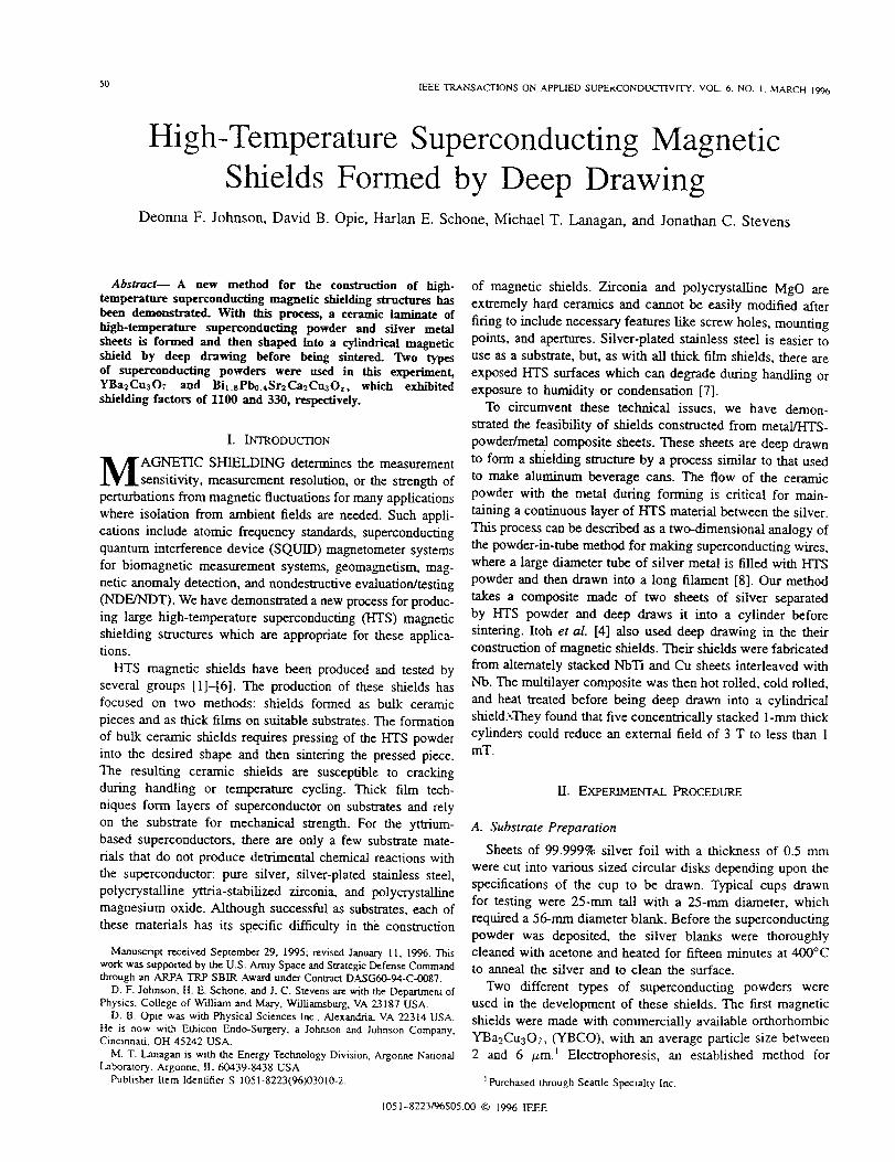
High-Temperature Superconducting Magnetic
Shields Formed by Deep DrawingDeonna F. Johnson, David B. Opie, Harlan E. Schone, Michael T. Lanagan, and Jonathan C. Stevens
Abstract--A new method for the construction of high-temperature superconducting magnetic shielding structures hasbeen demonstrated. With this process, a ceramic laminate ofhigh-temperature superconducting powder and silver metalsheets is formed and then shaped into a cylindrical magneticshield by deep drawing before being sintered. Two typesof superconducting powders were used in this experiment,YBa2Cu307 and Bix.sPbo.4Sr2Ca2CuaO_, which exhibitedshielding factors of 1100 and 330, respectively.
I. INTRODUCTION
'AGNETIC SHIELDING determines the measurementsensitivity, measurement resolution, or the strength of
perturbations from magnetic fluctuations for many applications
where isolation from ambient fields are needed. Such appli-cations include atomic frequency standards, superconducting
quantum interference device (SQUID) magnetometer systems
for biomagnetic measurement systems, geomagnetism, mag-
netic anomaly detection, and nondestructive evaluation/testing(NDE/NDT). We have demonstrated a new process for produc-
ing large high-temperature superconducting (HTS) magnetic
shielding structures which are appropriate for these applica-tions.
HTS magnetic shields have been produced and tested byseveral groups [1]-[6]. The production of these shields hasfocused on two methods: shields formed as bulk ceramic
pieces and as thick films on suitable substrates. The formation
of bulk ceramic shields requires pressing of the HTS powderinto the desired shape and then sintering the pressed piece.
The resulting ceramic shields are susceptible to crackingduring handling or temperature cycling. Thick film tech-
niques form layers of superconductor on substrates and rely
on the substrate for mechanical strength. For the yttrium-based superconductors, there are only a few substrate mate-
rials that do not produce detrimental chemical reactions with
the superconductor: pure silver, silver-plated stainless steel,
polycrystalline yttria-stabilized zirconia, and polycrystallinemagnesium oxide. Although successful as substrates, each of
these materials has its specific difficulty in the construction
Manuscript received September 29, 1995; revised January 11, 1996. This
work was supported by the U.S. Army Space and Strategic Defense Command
through an ARPA TRP SBIR Award under Contract DASG60-94-C-O087.
D. F. Johnson, H. E. Schone. and J. C. Stevens are with the Department of
Physics, College of William and Mary, Wdliamsburg, VA 23187 USA.
D. B. Opie was with Physical Sciences Inc., Alexandria. VA 22314 USA.
He is now with Ethicon Endo-Surgery, a Johnson and Johnson Company,
Cincinnati, OH 45242 USA.
M. T. Lanagan is with the Energy Technology Division, Argonne Nauonal
Laboratory. Argonne. IL 60439-8438 USA.
Publisher Item Identifier S 1051-8223(%)03010-2.
of magnetic shields. Zirconia and polycrystalline MgO areextremely hard ceramics and cannot be easily modified after
firing to include necessary features like screw holes, mountingpoints, and apertures. Silver-plated stainless steel is easier to
use as a substrate, but, as with all thick film shields, there are
exposed HTS surfaces which can degrade during handling orexposure to humidity or condensation [7].
To circumvent these technical issues, we have demon-
strated the feasibility of shields constructed from metal/HTS-
powder/metal composite sheets. These sheets are deep drawnto form a shielding structure by a process similar to that used
to make aluminum beverage cans. The flow of the ceramicpowder with the metal during forming is critical for main-
taining a continuous layer of I-ITS material between the silver.
This process can be described as a two-dimensional analogy of
the powder-in-tube method for making superconducting wires,where a large diameter tube of silver metal is filled with HTS
powder and then drawn into a long filament [8]. Our method
takes a composite made of two sheets of silver separatedby HTS powder and deep draws it into a cylinder before
sintermg. Itoh et al. [4] also used deep drawing in the theirconstruction of magnetic shields. Their shields were fabricated
from alternately stacked NbTi and Cu sheets interleaved with
Nb. The multilayer composite was then hot rolled, cold rolled,and heat treated before being deep drawn into a cylindrical
shield.,-They found that five concentrically stacked 1-mm thickcylinders could reduce an external field of 3 T to less than 1mT.
I1. EXPERIMENTAL PROCEDURE
A. Substrate Preparation
Sheets of 99.999% silver foil with a thickness of 0.5 mm
were cut into various sized circular disks depending upon the
specifications of the cup to be drawn. Typical cups drawnfor testing were 25-mm tall with a 25-mm diameter, which
required a 56-ram diameter blank. Before the superconductingpowder was deposited, the silver blanks were thoroughlycleaned with acetone and heated for fifteen minutes at 400°Cto anneal the silver and to clean the surface.
Two different types of superconducting powders were
used in the development of these shields. The first magnetic
shields were made with commercially available orthorhombicYBa_CuaOT, (YBCO), with an average particle size between2 and 6 /zm. I Electrophoresis, an established method for
1Purchased through Seattle Specialty Inc.
1051-8223/96S05.00 © 1996 IEEE

IOHNSON ¢f al.: HIGH-TEMPER.ATURE SUPERCONDUC'I2NG MAGNETIC SHIELDS 51
Silver
Fig. I. A silvedHTS-powder/silver composite made from 0.S-ram silver foil
plus 100 _m of HTS powder.
depositing powders in a liquid medium by an applied electric
field [9], was used to deposit YBCO on the silver substrate.The deposition of Bit.sPbo.4Sr2Ca2Cu30_ (BSCCO), a lead-
doped mixture of 2212, Ca2CuO3, and CuO, 2 could not be
preformed using electrophoresis because the mixture would
separate during deposition. Application of BSCCO to thesilver substmte was done through suspending the powder in
1-Butanol and relying on the surface tension of the butanol to
hold the suspension on the substrate. The butanol evaporated
and left a layer of BSCCO. These methods permitted us to varythe thickness of the HTS layers deposited on each substrate.
For results shown in this paper, the thickness of the HTS
layer on each silver substmte was 50 #m. Once the individualsilver disks were coated with HTS powder, a silver/HTS-
powder/silver composite sandwich was assembled with a total
powder layer of 100/zm (Fig. 1). This fiat composite was then
drawn into a cylindrical magnetic shielding structure.
B. Deep Drawing
Deep drawing is a well-established process for produc-
ing thin-wall objects of relatively large heights from thin,
fiat sheets by imposing suitable restraining and deformingforces [10]. Cylindrical (cup-shaped)superconducting mag-
netic shields, the simplest shape produced by this process,
are constructed by deep drawing the silver/HTS-powder/silvercomposites. To form a cylindrical cup from a flat blank, theblank is laid on a die which has a round hole in the center.
A punch descends axially through the hole which forces theblank over the rounded edge of the die (Fig. 2). For thedraw to be successful, the metal must flow smoothly to avoid
longitudinal folds, or wrinkles, in the walls. The success ofthe deep drawing process is due to the existence of tangential
compressive and radial tensile stresses that produce favorableconditions for deformation. The magnitude of the tensile stress
produced must be less than the ultimate tensile strength of thematerial.
For tall structures, it is seldom possible to produce afinished workpiece in one draw. Several redraws are frequently
necessary. In order to draw full-sized cups, we fabricated adouble-action press with a hydropneumatic die cushion system
to apply a controllable force on the blank.holder that holds
the outer periphery of the blank flat and prevents wrinklingduring the draw. Although very ductile, high-purity silver does
not draw well because it rapidly work-hardens. The work-
hardening causes wrinkles that frequently form about midwaythrough the draw. Prevention of these wrinkles has been the
greatest difficulty encountered. Another problem with silveris its extremely low tensile strength: 120-170 MPa when
2Supplied by Argonne National Laboratory.
_ Punch
(a)
@
Punch
Co)
Fig. 2. Schematic cross section of the (a) draw and (b) redraw in the
formation of cylindrical magnetic shields using deep drawing.
Fig. 3. Cylindrical HTS magnetic shields formed by deep drawing.
fully annealed. Any nicks or irregularities can cause localized
stresses to exceed the tensile strength of the material and lead
to the rupture of the shield wall.
C. Cup Sintering
The shields were sintered once the mechanical shaping
was complete (Fig. 3). The YBCO magnetic shields weresintered in an oxygen atmosphere at 910°C for 24 hours.
Sintermg temperatures higher than this were difficult due tothe lowered melting temperature of silver in an oxygen atmos-
phere. The cooling rate was 5°C/h from 910--860°C, 60°C/hfrom 860--510°C, and 5°/h from 510-200°C. The BSCCO
magnetic shields were sintered using a method developedfor the two-powder process designed for rapid formation
52 IEEE TRANSACTIONS ON APPLIED SUPERCONDUCTIVITY, VOL. 6. NO. I, MARCH 1996
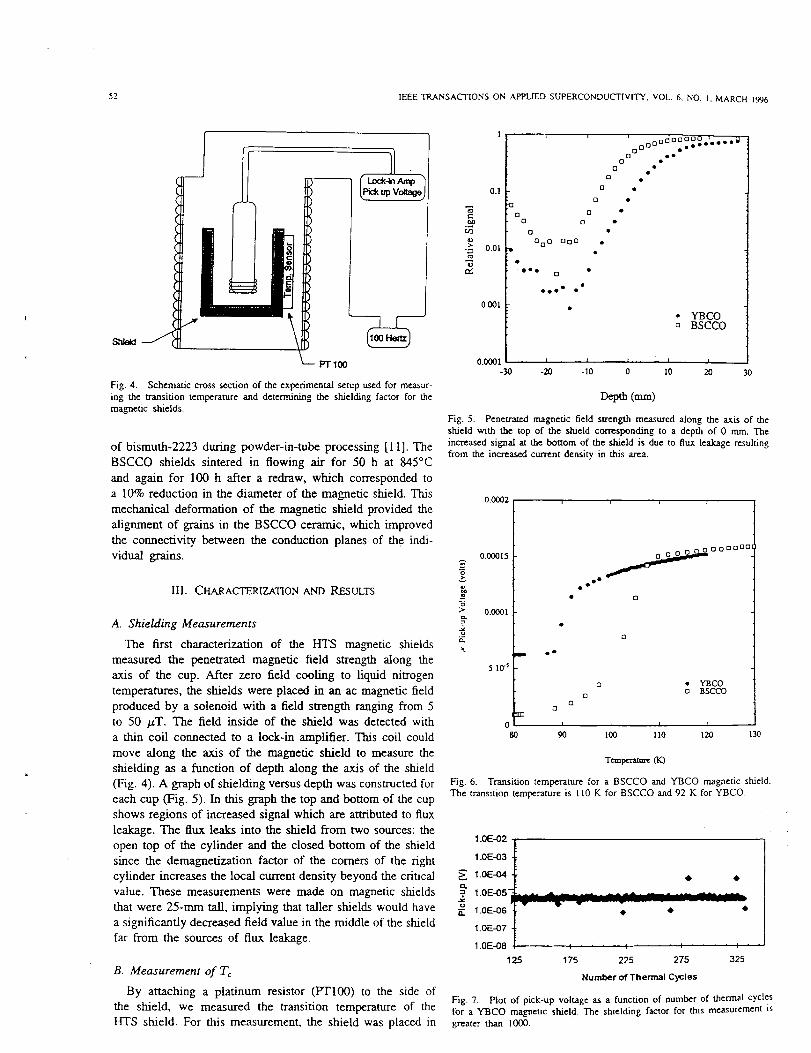
PT100
Fig. 4. Schematic cross section of the experimental setup used for measur-ing the transition temperature and determining the shielding factor for themagnetic shields.
of bismuth-2223 during powder-in-tube processing [11]. The
BSCCO shields sintered in flowing air for 50 h at 845°C
and again for 100 h after a redraw, which corresponded to
a 10% reduction in the diameter of the magnetic shield. This
mechanical deformation of the magnetic shield provided the
aligtlment of o_-ains in the BSCCO ceramic, which improved
the connectivity between the conduction planes of the indi-
vidual grains.
m. CHARACTERIZATION AND RESULTS
A. Shielding Measurements
The first characterization of the HTS magnetic shields
measured the penetrated magnetic field strength along the
axis of the cup. After zero field cooling to liquid nitrogen
temperatures, the shields were placed in an ac magnetic field
produced by a solenoid with a field strength ranging from 5
to 50 _T. The field inside of the shield was detected with
a thin coil connected to a lock-in amplifier. This coil could
move along the axis of the magnetic shield to measure the
shielding as a function of depth along the axis of the shield
(Fig. 4). A graph of shielding versus depth was constructed for
each cup (Fig. 5). In this graph the top and bottom of the cup
shows regions of increased signal which are attributed to flux
leakage. The flux leaks into the shield from two sources: the
open top of the cylinder and the closed bottom of the shield
since the demagnetization factor of the comers of the right
cylinder increases the local current density beyond the critical
value. These measurements were made on magnetic shields
that were 25-mm tall, implying that taller shields would have
a significantly decreased field value in the middle of the shield
far from the sources of flux leakage.
B. Measurement of Tc
By attaching a platinum resistor (PT100) to the side of
the shield, we measured the transition temperature of the
HTS shield. For this measurement, the shield was placed in
r./3
0.1
0.01
0.001
' odooooo , .@ i0000 oo ooO°°°
Q oo0 •
o •
o •
O •
0 •
0 0 •0 0 •
0
000 000 •
6Olo •
0
OoO •
• YBCOo BSCCO
0.0001 i L B i i
-30 -20 -10 0 I0 20 30
Depth (ram)
Fig. 5. Penetrated ma_aedc field strength measured along the axis of the
shield with the top of the shield corresponding to a depth of 0 ram. The
increased signal at the bottom of the shield is due to flux leakage resulting
from the increased current density in this area.
0.0002
="5>
E
0.00015
0.0001
im
5 lff _
m
0
8O
oo
i__ 0000001
° oo°
• 0
o o YBCOBSCCOo
£3o
i t i
90 I00 110 120 130
Tcmpc:-aam: (K)
Fig. 6. Transition temperature for a BSCCO and YBCO magnetic shield.
The transition temperature is 110 K for BSCCO and 92 K for YBCO.
1.0E-02
1.0E-03
>_ 1.0E--04
=, 1.0E-05"
_- 1.0E-06
1.0E-07
1.0E-08
125
: I : .... I ' •
175 225 275 325
Number of Thermal Cycles
Fig. 7. Plot of pick-up voltage as a function of number of thermal cycles
for a Y'BCO magnetic shield. "['he shielding factor for this measurement is
greater than 1000.
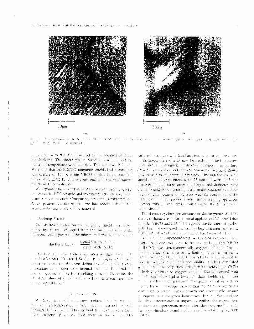
(r t !20um
J_
i!,,3 F!]AI]!'[ !T_I]:I, ',_I[_l llll[)U_[iC%
_ Ot£F'FI
Ibl
,: ,,,[cmmt w:th the delectlon coil m :he ]oc::t],_:_ ,,T i:tci_
e,: _hmldin g. Fhe shield was allowed ,u_ w:u-m ._p :rod the
::a[].,tt:,m teRipcraturc was recorded. Ftm; 1,_ Nhc,,,_.r ]rTt:]_: :
'?,c :,4rod that the BSCCO magneuc shmld_, had a t:ansm,m
temperature of I10 K while YBC() shield:-, had :_ ::-:ms:!ran
temperature at ')2 K This is consistent with out cxpecLm,_n,
:,_r 'best HIS ma[enal:,
V',c ,cparated :he .;1]vet [avers of the a]re:M,, -,:nk'red ,h>'l,]
::_ _"_p_>;e :he }IT:'; ceramic and invest:gated the pha,c, pr-_e:?:
;i'-,1[!,_: .k r:t t, d[lllTadtlOrl. (7ompanng our -,ample,; \,,:th :ercr_':;c:t
X ra,. pat:crux c,mtqrmed :hat we had rea:ched :h:? ._.,rrc,.:
,upcI_,[?ductl:lg pha,;c o[ :he ma:er;al
l-h:"d::eld:n_: ::icier Ior the magnehc _h)c],i, ,,:_ ,/'::':
IlllrlCd }7,',. tile r;.ttl_> OI hl_ilal trOIll _lt2 lllfler C(}I] & ]t}t,t_l: :2it'
:llaCnc::c '-,hie]d present to :he minnnum q£na) 'atTh :::u .h::'i ]
signal without sh]e]:],;hleldln_: factor
signal w::h ",hicld
[he best que!dm 7 Iactors recorded t_: ,.]:i::' ._:'::" :}1}_1
:.,: "YBC() and :'_()for BSCCO h :s m]p:_rT.m: :,, n,.::'
:!:at re-,catcher,, use dilfercnt dcfiniti:m:, ,_I _h:cld:::_ :__:,,r
<IUI"C:l,.]lllg tlpOll [hel[ ::xpenrnental IIIcIho'.t l-hi, [,.'tt,],, [,,
'.ar]ot,: quoted valuc_, i'or shielding Iaclo:,. "!t]erc:,_rc. :h,.'
;_b't,d:::cvaluc_ ,::d::clding fact r_ Ii-o111i]ifJoy:':l:::4[Wl. 4:7
:;,,:, 'reparable :21
_LIIILt_L)'. h'_ dcqrade "_lth ilalidllFl_, hulllldl:}, or coiidc:l:-,atl:_rt
F::_her:m_re. these sh:elds n:a_ be eas:l_ :nodilied :,?r5crc_
}h:]e, all:J ,_Iher Ct:TlU[l/O[l COIl,-,II11CIIO[l t:2aTtJFe_, Filial['.. d:2c[_
dra,amg :s a common ind,astnal technique that we ha',:" show ::
:(: ',_ork w:th metal, ceranuc laminates Alth ?uoh the ,maeneI:_
-,h:clJ: :,,r this experiment were 25-mm tall w:th a :.?.5 ran:
<hame:cr. duelds three times the height 4nd diameter v, er:.
Jr::wn V',nnkIin_ :x a hlllltlll:: lacier In [}!e product_o:: ,:: the> +
)ar_'e: ,Melds because _: mlertere_ with the continu::', ,_: The
fits p,_,.der Better proccs,, c,mmq in the Jra,.vmg oper::::on.
to_ether," ','.ith a Itir2erpre_s, v,c, uld enable :he tor:naT:,m _!t
]ar_zer>h:elda
II:c thermal cycling pcrlormancc el the :nagnetlc <h:eld :,,
i CTIIICiI: chiLFactenstlC lot pr:tct]calappllc::::on We :<,u::d:hat
b ,dr :h:" YBCO and BS(('() magnet:c sh::-],i>ther::::d.".,ic,i
_kell }'1:1 7 ",ho`'L", ,zzot:d [hcTll/4! ,_'yChFl_: ,Jhdr:lcteFl',::,_-..:::r 3
YB('() _hle]d v,h:ch :txhibilcd a s lie d n2. TLlctor ,_t : 1:'_)
"\HI*ltJ::}i h:lC <upcrcondudor _as seuied bc[_cc:: qlxc:
]a',er,, there dot', a,,I seem 1_ bc ;my c`':dence :)la[ l'B('()
,_r BS(('() ,aas ,I,qchiomctrlcallx oxyge:: doric:on: It::'. :,
,::It b_ :he ]act that 'qlVCl 41 :he hi}:h sH:Tcr];]_ tempcr::ture_,
";4: ( :o: BS('('() and otl) (" {_r YB('{_ :-. transparent _,,
_x}:2.c:l \Ve al,;_ '._41:1d :h;:: The qualit:. ,'T s:l_cr C,VTe[C:ted
v. lth the shle]diI:_: pr_:pcrtk's (q the ":'Bet ) -k::.'ld.,, since ':'B('( 1
:,.hi,_,h]\-:cn>,:u',vr :o _x?,:.tcn content Si:mids tort:red ',_tt):
')_a :}"; [:tlre _i]v:': h4d a [o`'veF ,,: lha!1 Qlk'Id>, r:l;uic :Foil:
')() :)Q:J"; ,l]`'c': }{_,:::H1111:tIl:q) 01 lhc qtla[I[', :q ;<It\el &1:}i At:
a[k)llllC t(l[Ct" IlllL'IO',COpC" ",)l()'_C:J that [_c" ')q :'Jr:: ),i]`'e/ had a
'-,l,'2r]lll_ An! ic*,ltl_.:l_[: Irk tZI;tlll '_Fk)\t. rltl ,iIld L! :l_',tic:-atTJP cHIOtlI12
,_ tll)::11:]t]:'\:it:}iv '::i :l h,mr:daile> (}:_ NI \V:, .,,r:ciLa]C
:hLi! [t'11', CO[IL':_HTT:i:]_::: ::I [II1:?11:i:l:"_ lIlhii:l:< !hO :"," 'q _]_,:r]l
ICLI_.:]I[]L" :!?C ",:l:)C:,':l[l(illk :I[):' I:i)',kL]('|. '[]Ir2:t'!'',, _[]T:?}ll![]:IQ I__
:hi2 [:,','[ ")'l)Cl,!):L:' :,_[]II_t It,:!:: LI'q:ILL lilt.' _,i ,)'; q',,d \_::h
YB(()
54 IEEE TRANSACTIONS ON APPLIED SUPERCONDUCTIVITY, VOL. 6. NO. I. MARCH 1996
ACKNOWLEDGMENT
The authors wish to acknowledge the contributions to this
work from S. RemiUard and L. J. Klempter, Illinois Super-
conductor; Profs. M. Hinders and D. Manos, Department of
Applied Science, College of William and Mary; Dr. J. Bensel,
Physics Department, College of William and Mary; and T. V.
Prather, Physical Sciences, Inc.
REFERENCES
[1] IC Hoshino, H. Ohta, E. Sudoh, IC Katoh, S. Yamazaki, H. Takayama,
H. Takahara, and M. Aono, "Magnetic shield of high-Tc Bi-Pb-Sr-Ca-
Cu-O superconductors at 77K for SQUID measurements," IEEE Trans.
Magrt, vol. 27, pp. 2202-2205, 1991.[2] G. J. Cui, S. G. Wang, H. M. Jiang, J. Z. Li, C. Y. Li, C. D. Lin,
R. Z. Liu, Q. L. Zheng, Y. S. Fu, Z. L. Luo, and W. C. Qiao, "A
superconductive shielding can for high Tc SQUID," IEEE Trans. Magn.,
voi. 25, pp. 2273-2275, 1989.[3] M. Roll H. Ishigaki, and T. Ohyama, "'Effect of Ag on magnetic shield
of superconducting Y-Ba-Cu-O cylinders," Cryogenics, vol. 30, pp.
863-867, 1990.[4] I. Itoh, T. Sasaki, S. Minamino, and T. Shimizu. "Magnetic shielding
properties of NbTffNb/Cu multilayer composite robes," IEEE Trans.
Appl Superconduct., vol. 3, pp. 177-180, 1993.[5] J. O. Willis, M. E. McHen_ry, M. P. Maley, and H. Sheinbe_, "Mag-
netic shielding by superconducting Y-Ba-Cu-O hollow cylinders," IEEE
Trans. Magtt, vol. 25, pp. 2502-2505, 1989.[6] M. M. Miller, T. Carroll, R. Soulen, Jr., L. Toth, R. Rayne, N. McN.
Alford, and C. S. Saunders, "'Magnetic shielding and noise spectrum
measurement of Y-Ba-Cu-O and (Bi,Pb)-Sr-Ca-Cu-O superconducting
tubes," Cryogenics, rot. 33, pp. 180-183, 1993.[7] D. B. Opie, "Advanced composite laminates for forming high tem-
perature superconducting magnetic shields,'" Physical Sciences, Inc.,
Alexandria, VA, Phase I SBIR Final Rep., Contract DASG60-94-C-
0087, 1995.
[8] D. Y. Kaufman, M. T. Lanagan, S. E. Doms, J. T. Dawley, I.D. Bloom, M. C. Hash, N. Chen, M. R. DeGuire, and R. B.
Poeppel, "Thermomechanical processing of reacfvely sintered Ag-
Clad (Bi.Pb)2Sr2Ca2Cu3Oz tapes," Appl. Superconduct, vol. I, pp.81-91, 1993.
[9] B. Zhang, P. Fabbricatore, G. Gemme, R. Musenich, R. Parodi, and L.
Risso, "Preparation and characterization of Y'Ba2Cu3OT-x supercon-ducting films deposited by electrophoresis," Physica C, vol. 193, pp.
1-7, 1992.
[10] AMS Int., Metals Handbook, 14, Forming and Forging, Metals Park,
OH, 1988.[11] S. E. Dorris, B. C. Pmmk, M. T. Lanagan, S. Sinha, and R. B. Poep-
pel, "'Synthesis of highly pure bismuth-2223 by two-powder process,"
Physica C, vol. 212, pp. 66-74, 1993.[12] J. Wang and M. Sayer, "High temperature superconductors for low
frequency magnetic shielding," IEEE Trans. Appl. Superconduct., vol.
3, pp. 185-188, 1993.
Deonna F. Johnson received the B.S. degree in physics from Bethany
College, Bethany, WV, in 1992, and received the M.S. degree from the Collegeof William and Mary, WtUiamsburg, VA, in December 1994.
She is currently a physics Ph.D. candidate at the College of William and
Mary, where she is working in the field of nondestructive evaluation focusingon the application of thermoelasficity.
David B, Opie received the B.A. degree in physics from the University ofDelaware, Newark, in June 1986. He received the M.S. degree in June 1988
and the Ph.D. degree in December 1991, both from the College of william
and Mary, W'dliamsburg, VA.
While at William and Mary, his research was directed toward the devel-
opment of a compact hydrogen maser frequency standard and applications
of high-temperatm'e superconductivity. From 1991 to 1995, he was with
Physical Sciences Inc., Alexandria, VA. His research interests were focused
on the applications of high-temperature superconductors, compact frequency
standards, and nondestructive evaluation. Currently, he is a Principal Scientist
at Ethicon Eado-Surgery, a Johnson and Johnson Company. His research
interests are directed toward applying electromagnetic, ultrasonic, and laser
technology to the development of medical devices.
Harlan E. Schone received the B.S. degree in engineering physics from
the University of Illinois, Orbana, and the Ph.D. degree in physics from the
University of California, Berkeley. in 1961.
He was employed at Boeing Research Lab from 1961 to 1965 and has
been on the faculty at the College of William and Mary, williamsburg, VA,
since 1965. He has worked in the area of electronic properties of metals using
NMR and muon spin rotation techniques. Recent work has involved studies
of the effect of hydrogen on the electronic properties of high-temperature
superconductors.
Michael T. Lanagan received the B.S. degree in ceramic engineering from
the University of Illinois, Urbana, and the Ph.D. degree from Penn State
University, University Park_At Penn State, he studied the microwave dielectric properties of ferroelectric
and antiferroelectric materials. He joined Argonne National Laboratory in
1987, where he presently explores the electrical and mechanical properties
of high-temperature superconductors. His work encompasses synthesis and
fabricatiomof superconductors, fuel cells, and dielectric ceramics. In addition,
he has been with IBM and Coming Glass. He has authored or coauthored
over 100 publications in the field of electronic ceramics.
Jonathan C, Stevens received the B.S. degree in computer science from the
College of W-tlliam and Mary, Williamsburg, VA, in 1993.
He is currendy working as an independent designer of electronic and me-
chanical equipment for material testing. He developed the drawing techniquesfor this work.
Displacement Compensation of Temperature Probe
Christopher S. WelchSenior Research Scientist
Applied Science Department
College of William and Mary
Williamsburg, VA 23187
James A. Hubert
6780 Deer Bluff Drive
Dayton, Ohio 45424
Patrick G. Barber
Professor and Co-director of Chemistry
Department of Natural Sciences
Longwood College
Farmville, VA 23909
Data
KEYWORDS
Temperature Probe Measurement, Conductivity Error, Displacement Compensation,
Temperature Profile Measurement
ABSTRACT
Analysis of temperature data from a probe in a vertical Bridgman furnace growing
germanium crystals revealed a displacement of the temperature profile due to
conduction error. A theoretical analysis shows that the displacement compensatiov: is
independent of local temperature gradient. A displacement compensation value
should become a standard characteristic of temperature probes used for temperature
profile measurements.
TEMPERATURE PP, OBE COMPENSATION
When temperature probes are used to measure the temperature of surrounding fluids,
liquids, or gases, correctior:s are frequently made to the raw temperature data. These
corrections are intended to account for rapid temporal and spatial changes of the
environmental temperature, direct heating of the probe through absorption of
cadiation, and conductive heat loss through the structure supporting the sensitive
ele,nent. For each of these corrections, formulas have been developed over the years
and are aw_ilable in handbooks so that practiti_u_ers can have access to ready guidance.
I:or thermocoup[e nmast, remel_ts a teference such as Moffatt [1962] is among those
available. [n general, these formulas provide correction values of temperature to be
applied at the positiot_ ascribed to the sensitive element of the probe. This paper reports
another interpretation which applies a correction to the position, rather than the
temperature, of the sensitive element. [n some cases, a displacement correction is cnore
it-_tuitive and somewhat simpler than the temperature correction.
DISCREPANCY BETWEEN RADIOGRAPHIC AND TEMPERATURE
PROBE MEASUREMENTS
The motivation for this work came from an experiment in which the position of the
mett-solid ir_terface in a vertical Bridgman furnace used for the growth of germanium
crystals was estimated by two independent methods: x-ray radiography and temperature
profile measurements from a thermocouple probe. The objective of the experiment was
to verify whether thermocoupte measurements could be used to monitor crystal
growth.
The furnace coctsisted of two nearly isothermal sections maintained at approximately
1100 K in the lower section and 1270 K in the upper section. The temperatures of these
two sections bracketed the 1210 K melting point of germanium. With this furnace
configuration the melt-solid interface can be kept in the 3 cm regior_ between the
isothermal zones during most of the growth. A schematic diagram of the experimental
setup is shown in Figure 1.
Because the solid actd liquid phases of germanium differ in density by 4%, the melt-
solid boundary could be measured using x-ray radiography. Measurements were made
from radiographic images on film, and the boundary location was estimated by
measuring the position of the interface with respect to fixed objects which provided
fiducial locations on the film. One of the features visible on the film is the tip of the
thermocouple probe, providing a verification of the position measureme__t of the
probe.
The temperatures were measured using a thermocoupte which moved inside a
centerline capillary tube. The capillary tube was fabricated as part of the sample ampule
[Hubert, et al, 1993]. Because the thermal conductivity of the liquid and crystalline
phases of germanium differ, the interface location could be esticnated using a plot of the
temperature vs position data obtained by the thermocouple in tim centerline capillary.
The location of the interface was postulated as the p_int at which the slope of the
temperature versus positioc_ data chal_ges. This assumes that heat flux is primarily axial
in the cylindrical germanium sample and continuous through the interface. The
difference in thermal conductivity requires a compensating difference in ternperaturegradient to maintain continuity ill the heat flux. It_ tile measured data, the sharp breakin temperature gradient was smoothed by conduction effects, so the position wasdetermined as the intersection of two straight lines fit by least squares to the data oneither side of the approximate position.
The positions of the melt-solid interface determined radiographically and thermallydiffered systematically by 3 mm, The melt-solid interface determined from the thermaldata was 3 mm into the liquid zone as determined by the x-ray measurements.
NUMERICAL MODEL OF PROBE TIP TEMPERATURE
Hubert [1992] constructed a series of numerical models to evaluate the radiation
environment and thermal flow in the entire furnace, including the thermocouple
probes. These models were designed and run to represent varying locations of the
thermocouples found in the experimental data. The results verified the experimental
observation that the temperature profile measured at the thermocouple tip is shifted 3
mm toward the liquid zone. The results also showed that the heat flow through the
sample is generally axial near the insulating region of the furnace. This result along
with the axial symmetry of the experiment allow a good approximation of the
thermocouple temperature end-effects to be obtained through one-dimensional
analysis.
MATHEMATICAL ANALYSIS LEADING TO DISPLACEMENT
INTERPRETATION
The formula given by Moffatt [19621 for correction of conduction error in
thermocouples used to measure temperatures in gas streams is
T T- Tj = (T T- TM)/cosh[L(4hc/d ks) 1/2] (1).
In this equation, TT represents the true temperature of the flowing gas stream being
sampled by the thermocouple, which is considered as extendir_g into the stream from a
wall of the experimental chamber or model surface. Tj is the temperature of the
thermocouple junction, so the left side of the equation corresponds to the conductiot_
error. TM is the temperature of tlle mount for the thermocouple, or the chamber wall. L
is the length of the thermocoup_e junction, hc is the coefficient of thermal transfer
between the junction and the surrounding gas, and k s is the thermal conductivity of
the junction along tile length of the wires. One way to visualize the thermocouple
described by this equation is as a long cylil_dct of length, L, much greater than its
diameter, d, extending from a flat mount with the junction temperature represented by
the temperature at the terminal end of tl_e cylinder. Equation ([) can be derived from a
one-dimensional analysis of the conductive heat equation on such a structure if the
heat flux through the top of the cylinder is neglected and the gas surrounding the
cylinder is considered to be isothermal with a constant thermal transfer coefficient.
The argument of the hyperbolic cosine in Eq. 1 contains many of the physical
parameters which determine the amount of conduction error. As the product of L,
which has dimensions of (length) I and the factor within the square root, must be
dimensionless, the factor within the square root must have dimensions of (length) -2.
The inverse of this factor can be interpreted as a product of two terms, each having the
dimension of (length) 1. As noted by Moffatt [1962], one of these, d/4, represents the ratio
of the area of a cross-section of the cylinder to its perimeter. The value of this factor can
clearly be altered by choosing different junction cross-sections, so the factor forms a
useful design parameter. The other factor, ks/ho is the ratio of the axial thermal
coctductivity of the junction to its heat transfer coefficient. This factor has dimensions
of (length) 1. The square root of the product of these factors occurs so often in the
analysis that we choose to give it a separate symbol, A, and treat it as the major
parameter of the analysis,
A = [(w/p)(ks/hc)] 1/2, (2)
wherew and pdenote respectively the area and perimeter of the cross section. In thisK
form, the argument of the hyperbolic cosine in Eq. 1 becomes (L/A), the ratio of the
junction length to a characteristic length.
To adapt this analysis to the environment of the Bridgman furnace, the most
important addition is a temperature gradient along the length of the probe. The
one-dimensional heat equation is theft
T"{x) - (1/A2)T(x) = -(a/A2)x, (3)
as given in Carslaw and Jaeger [1959].: The new parameter, a, denotes the thermal
gradient of the surroundings. If the cylindrical rod carrying the thermocouple is
considered to extend from negative infinity to x=() and the ambient temperature scale is
set to zero at x=0, , the solution is given as
T(x) = ax - aA exp(x/A), (x<0). (4)
At tlle tip (x=(J),the temperature t_f the surrounditt_s is zero, but that of the probe tip i_
-aA. This happens to be the temperature of the sttrrot, tu.]ings at Iocatior_ x=-A, s(+ (+ne
can interpret the difference as a ten_perature difference at the probe tip or alternately as
a displacement difference of the rneasurement location. If the displacement
interpretation is chosen, the correction needed does not depend on tl-te value of the
thern_al gradient, a value which is cu+_tavailable prior to the measurement.
CORRECTION TO DATA FROM TFIE BRIDGMAN FURNACE
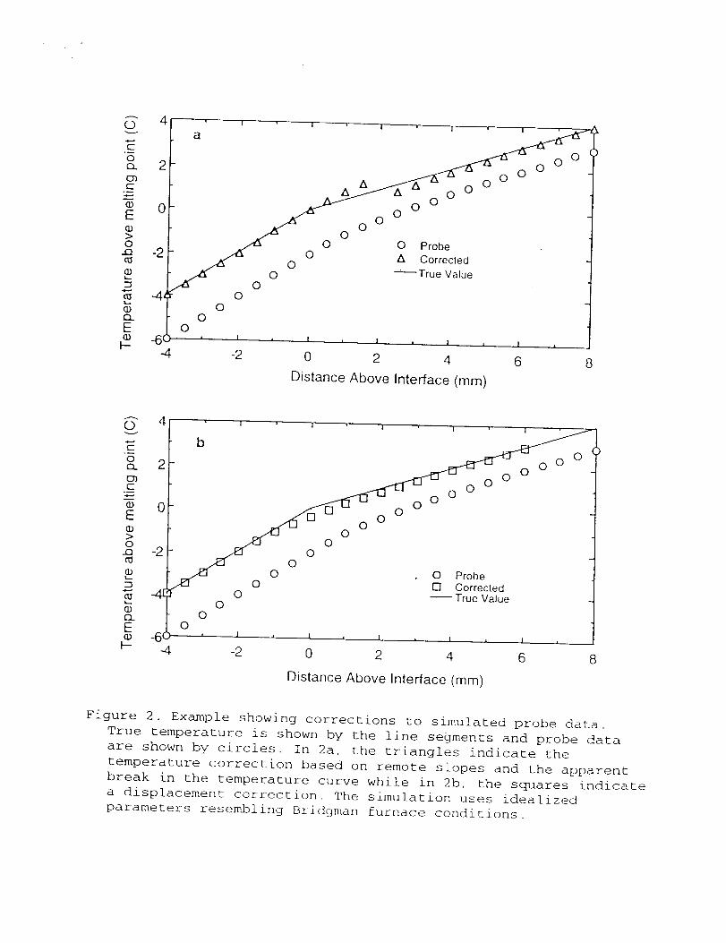
The Bridgman furnace provides an example wl-tich illustrates the difference between
adjusting for conduction in a thermocouple through a temperature correction and
through a displacement. The data are simulated for a material with exactly a two-to-one
ratio of thermal conductivities for the melt and solid phases respectively• Hubert [1992]
solved the linear l-teat equation for the temperature profile in a probe passing through
the interface itx this case. For a probe entering from the cold region, the tip temperature
isgiven by
Tj(x) =a(x-A),forx<0 (5)and
TI(x )=(ax/2)-(aA/2)(l+exp(-x/A)),forx>0, (6)
where Tj(x) denotes the tip tetnperature for a probe with its tip at location x, the
distance above the interface. Equations (5) and (6) are plotted as circles in Fig. 2a and 2b
for act example probe having a value for A of 2 ram, and the heat flow is chosen to
produce exactly a 1 degree/ram gradient in the solid phase and 0.5 degree/ram gradient• X,,
in the liquid phase. The temperatt.tre of the materml it1 this idealization is represented
by the solid lines. The change in slope of the probe temperatures is seen to occur
approximately 2 mm into the liquid phase of the material•
If a temperature correction is applied to these data, the correction is dependent of the
slope of the data• The data on either side of the observed change in slope can be
corrected by the corresponding amount and are represented by triangles in Figure 2a. As
shown, the data between the actual interface and the observed change in slope cannot
be properly corrected. Also, the data near the observed change in slope cannot easily be
used due to the curvature present. If linear curve fits are applied to the remainder of
the data, the approximate location of the actual interface can be found. However, this
process requires estimation of the slope of the data twice, which induces additional
error into the correction, and it cannot use all the available data.
lhe alterttative is simply t_+ apply the displacement correction A to the erttire data set,
thereby shifting+, t!_e ctttve appropriately. Figure 2b shrews the same rnaterial

temperature and measured values as figure 2a. Fhe squares represent tile displacemct_t
coFrection of A (2 ram) towards the s()lid region. This simple, uniform correction is
independent of the particular data, and its accuracy is given by I:he thermocouple and
environmental properties. The displacemevtt correction automatically produces an
appropriate correction for the conduction error associated with the measured
temperature values.
EXPERIMENTAL VERIFICATION
Barber, e¢ nl [1996] performed an experiment in which a thermocouple was used to
measure the temperature profile in a Bridgman furnace compared with a
radiographically determined phase interface with the thermocouple inserted from both
the cold zone and the hot zone of the furnace along a centerline capillary. The two
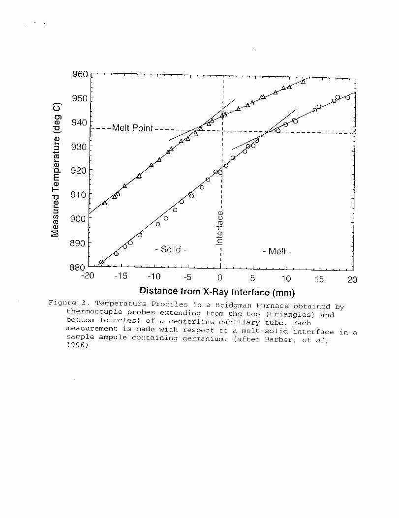
temperature profiles, shown in Figure 3, were displaced from one another by about 11
ram. The temperature error at the melt point was 5 K for the probe coming from the
hot zone and 16 K for the probe enterit_g from the cold zone. The breaks in the two sets
of lines differed in temperature by only 3 K. The midpoint between the two breaks in
the the lines fell within one degree K of the melt point of germanium and within 2
mm of the interface as determined from x-radiography. This finding agrees
substantially with the one-dimensional theoretical analysis. In this experiment, type R
thermocouples were used which have a significantly larger displacement correction
parameter, A, than the type K thermocouples used to obtain the data reported by Hubert
[1992]. As a further test of the hypothesis tl_at conduction error manifested in an end
effect was responsible for the spatial offset between the radiographicaIly determined
interface and that determined by probe measuremen'ts, Barber, et a1.[1996] constructed a
type "R" (Pt - Pt/10%Rhodium) thermocouple with one leg extending from the hot
region of the furnace and the other one extending from the cold region. The measured
break in the curves occurred well within 1 K of the melt point and slightly more than 1
mm from the radiographically measured ii'tterface. The remaining spatial offset may be
attributable to the difference in thermal conductivities of the two thermocouple
materials, the alloyed platinum having slightly less than half the thermal conductivity
_f the pure platinum.
CONCLUSION AND RECOMMENDATION
We coL_c[ude that conduct{vity erroL leads to a spatial offset iv_ temperature profile data
taken with the thermocouple probe in the Bridgman furnace e×periments. Because the
error arose from causes unrelated to the specifics _f the particular environment, we
c(_nclude that spatial offset is a general feature (_f temperature profile data obtained with
pn_bes. We recommend that the offset parameter, A, become a standard, reported
characteristic of temperature probes which are intended for use in temperature
profiling measurements.
ACKNOW LEDG EMENTS
The authors acknowledge the support of Archibald Fripp, Jr., who provided intellectual
guidance, laboratory fa(:ilities, and some financial support through NASA Grant NAG-
1-627 to one of the authors (P.G.B). Another author (C.S.W.) was supported in part by
NASA Grant NAG-l-1585 and its successors. Willard Bauserman, of NASA, shared
unselfishly his expertise and experience in thermocouple probe measurements and
techniques.
REFERENCES
1. Barber, P. G., A. L. Fripp, Jr., W. J. Debnam, Jr., G. Woodall, R. F. Berry and R. T.
Simchick, "Experimental verification of agreement between thermal and real time
visual melt-solid interface positions in vertical Bridgman grown germanium," J.
Crystal Growth I60, (March, 1996),55-58.
2. Carslaw, H. S. and J. C. Jaeger, Conduction of Heat in 5olids, 2rid ed. (Oxford
University Press, Oxford, 1959), p. 134.
3. Hubert, James A. Numerical thermal analysis of a sample of germanium with a
centerline capillary tube i_1 a vertical Bridgnlan FI_rnace, Master's Thesis, George
Washington University, Washington, DC (1992).
4. Hubert, James A., Archibald L. Fripp, Jr. and Christopher S. Welch, "Resolution of
the discrepancy between temperature indicated interface and radiographically
determined interface in a vertical Bridgman furnace," Journal of Crystal Growth
131, (1993), 75-82.
5. Moffat, R. J., "Gas Temperature Measurement," in Temperature: Its Measurement
and Control in Science and Industry, Vol. 3., Ed. C. M. Herzfeld, Part 2, Applied
Methods and Instruments, Ed. A. [. Dahl, (Reinhold Publishing Corporation, New
York, 1962), 553-57l.

...... A;"..,-I
,°_°.i V".'.'q",'.I
°..°'I
°_'-'I I
_°-'.I I
:::::::::I'-.'..'-i----
r'":?::: ,_.^
;-;.-.-::....-:I___.
F.'.-.:."-:: ,_.
_:?-<::r:::.::-'.::!:::.::::.::;:::":":': Ad'.:::.-::l:-'.-':"::i:::-'::.'.:
1t'
,°...i-,-.1
"''' I,','.I
'.'. I,'-'-I
.'.'.'.'.1 Hot Isathermal
.i+i_. Liner
Vacuum
_----'---_kictuid Phase• .
.__---- nsulating_,A e
•,._ _Centerline Capillarym
--Solid PhaseR _
/:".":-':I::::.::-.:t
::::.:::.-:1
-'i'..i'i!F],','..°. "°." 1., ,.
Cold IsothermalLiner
_Temperature Probe
Figure I. Schematic representation of the temperature measurement
apparatus in a Bridgman furnace used to monitor crystal growth.
The ampule can be moved to grow or me_t the solid phase, and the
temperature probe can be moved to sample different positions. The
drawing is not to scale.
O
C
O
r
E
>0r_cO
cl
E
I-.-
1
2
o
-2
.-Z
-6'
:oO°ooooOO
O O Probe ._..,.4_ O A Corrected
,_ O O --True ValueO
O
O
O
O, J i _ I _ I _ i _ I J ,
-2 0 2 4 6
Distance Above Interface (ram)
G 4v
c
Oo_ 2O3c"
._
e 0E
>O..(3 -2
E_ -6
' I ' I "" I ' | ' I _,i_ _'-'
b /ooO
o o
0 0 0 0 0 0_0 O
S 0 0 0
0 . 0 Probe0 [] Corrected
0 -- True Value
0
0
0i , ! , 1 i L A I L
-2 0 2 4 6 8
Distance Above Interface (mm)
Figure 2. Example showing corrections to simulated probe data.
True temperature is shown by the line segments and probe data
are shown by circles. In 2a, the triangles indicate the
temperature correction based on remote slopes and the apparent
break in the temperature curve while in 2b, the squares indicate
a displacement correction. The simulation uses idealized
parameters resembling Bridgman furnace conditions.
96O
95O
0
¢ 940
'L
930
r,, 920E
I--•"u 910
900
890
88O-20 -15 -10 -5 0 5 10 15
Distance from X-Ray Interface (mm)
Figure 3. Temperature Profiles in a Bridgman Furnace obtained by
thermocouple probes extending from the top (triangles) and
bottom (circles) of a centerline cabillary tube. Each
I
I
I •
..... M
/o !_so,,d_,i -Me,t,-,
2O
measurement is made with respect to a melt-solid interface in a
sample ampule containing germanium. (after Barber, et al,
1996)
Abstract Submitted
for tile Mar96 Meeting of
The American Physical Society
Sorting Category: 16.b
Time evolution of radiation-induced luminescence in
terbium-doped silicate glass MICHAEL S. WEST, The College of
William & Mary, WILLIAM P. WINFREE, NASA Langley Research
Center -- A study was made on two commercially available terbium-
doped silicate glasses. There is an increased interest in silicate glasses
doped with rare-earth ions for use in high-energy particle detection and
radiographic applications. These glasses are of interest due to the fact
that they can be formed into small fiber sensors; a property that can be
used to increase the spatial resolution of a detection system. Following
absorption of radiation, the terbium ions become excited and then emit
photons via 4f-4f electronic transitions as they relax back to the groundstate. The lifetime of these transitions is on the order of milliseconds.
A longer decay component lasting on the order of minutes has also beenobserved. While radiative transitions in the 4f shell of rare-earth ions
are generally well understood by the Judd-Olfelt theory, the presence of
a longer luminescence decay component is not. Experimental evidence
that the long decay component is due, in part, to the thermal release
of trapped charge carriers will be presented. In addition, a theoretical
model describing the time evolution of the radiation-induced lumines-
cence will be presented.
Prefer Oral SessionPrefer Poster Session
Michael West
west_physics.wm.edu
Department of Physics, The College of William _: Mary
Date submitted: February 12, 1996 Electronic form version 1.1