technology computer aided design (tcad) …rudan/materiale_didattico/dia...g. betti beneventi 1...
TRANSCRIPT

1 G. Betti Beneventi
Technology Computer Aided
Design (TCAD) Laboratory
Lecture 1, Introduction
Giovanni Betti Beneventi
E-mail: [email protected] ; [email protected]
Office: School of Engineering, ARCES Lab. (room Ex. 3.2), viale del Risorgimento 2, Bologna
Phone: +39-051-209-3773
Advanced Research Center on Electronic Systems (ARCES)
University of Bologna, Italy
[Source: Synopsys]

2 G. Betti Beneventi
About the course 1/2
• The main part of the course will be devoted to the practical use of a
commercial TCAD software. The activities will be held in the ARCES
Lab (room Ex. 3.2).
• The two fundamental questions What is TCAD? Why TCAD? will be
answered in this lecture.
• Some theoretical background will be introduced as well to provide a
mathematical and physical foundation to support the TCAD activities.
The theoretical lessons will be delivered by Prof. M. Rudan.
• The exam consists in two tests:
– A TCAD design project strictly related to the content of the course.
The project will be carried out by the students during the last week of
the course, directly during the course class, in the ARCES Lab (room
Ex. 3.2).
– A questionnaire about the theoretical background part
– No mark will be given, the outcome will be either ‘passed’ or ‘not
passed’
3 G. Betti Beneventi
About the course 2/2
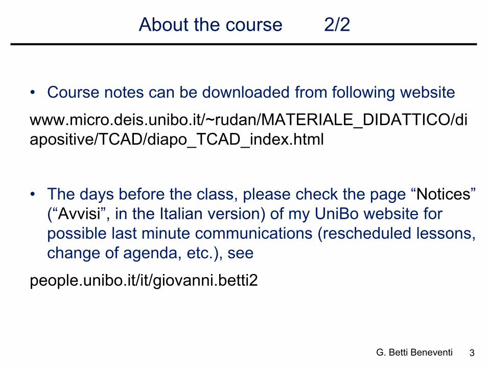
• Course notes can be downloaded from following website
www.micro.deis.unibo.it/~rudan/MATERIALE_DIDATTICO/di
apositive/TCAD/diapo_TCAD_index.html
• The days before the class, please check the page “Notices”
(“Avvisi”, in the Italian version) of my UniBo website for
possible last minute communications (rescheduled lessons,
change of agenda, etc.), see
people.unibo.it/it/giovanni.betti2

4 G. Betti Beneventi
Outline
• Physical Modeling
• What is TCAD?
• Why TCAD?
• A link to the context
• In this class
• To probe further
5 G. Betti Beneventi
Outline
Physical Modeling
• What is TCAD?
• Why TCAD?
• A link to the context
• In this class
• To probe further

6 G. Betti Beneventi
Physical modeling: definitions
Physical Modeling
Representation of the physical behavior of a system (device) by an abstract
mathematical model which approximates this behavior. Such a model may either
be a closed-form expression (analytical model), or, in general, a system of
coupled (differential) equations to be solved numerically.
Analytical Modeling vs. Numerical Modeling
Analytical modeling basically means the representation of a physical property
or law in terms of approximate closed-form expressions using “lumped”
parameters. It is also called “compact” modeling.
Numerical modeling: modeling of the device behavior through the numerical
solution of the differential equations describing the device physics on a given
geometrical domain.
Note: In the literature, the word “modeling” usually implies analytical/compact
modeling, while “simulation” is much used for numerical modeling.

7 G. Betti Beneventi
Examples
• Analytical modeling
– IDS-VDS curve of a MOS transistor
• Numerical modeling
– Drift-Diffusion numerical model solved at each node of a
discretized domain

8 G. Betti Beneventi
Physical modeling: Pros & Cons
• Analytical Modeling
Captures the essential concepts of device physics.
Very effective to single out the most important aspects of a problem.
Computationally efficient. Statistical analysis can be afforded.
Limited applicability: hard to describe problems with complex geometry or very
rich physics (e.g., “multiphysical” problem, i.e. coupled equations).
New, physical models need significant a-priori understanding of the problem and long
developing times.
• Numerical Modeling
Allows for the description of more complex phenomena (physics & geometry).
Addresses also problems that do not have a closed-form solution.
More flexible, does not always need a depth a-priori understanding of the problem.
More reliable from a quantitative point of view.
High computational burden. Statistical analysis hard to be afforded.
More difficult framework to interpret the results and to single out essential points.
Require complex software architectures or expensive licenses of commercial tools.

9 G. Betti Beneventi
Physical modeling of semiconductor devices
• Analytical and numerical modeling are complementary techniques, that are
often used together in both industry and academia, with different specific
aims. In the semiconductor device field, compact models and numerical
simulation are expected to interact with each other in the semiconductor
chip design flow (see next).
• Nowadays, in the semiconductor industry compact models are mainly used
for circuit-device interaction (circuit simulators), statistical analysis and on-
the-fly screening of experimental results.
• Numerical simulation is much used to understand advanced device physics,
for device design, scaling analyses & interaction with process
manufacturing.
• Of course, any kind of modeling should always be validated (or, in some
cases, calibrated) with respect to the available experimental data.
• This course will be about numerical modeling of semiconductor devices,
usually named as TCAD, which stands for “Technology Computer-Aided
Design” (see next).
10 G. Betti Beneventi
Outline
• Physical Modeling
What is TCAD?
• Why TCAD?
• A link to the context
• In this class
• To probe further

11 G. Betti Beneventi
What is TCAD?
• TCAD = Technology Computer-Aided Design
TCAD is a branch of Electronic Design Automation (EDA) that models semiconductor
fabrication and semiconductor device operation. The modeling of the fabrication is
termed Process TCAD, while the modeling of the device operation is termed Device
TCAD. The aim of TCAD is the design of semiconductor processes and devices to fulfill
some given specifications.
• Process TCAD: modeling of semiconductor-chip process-manufacturing steps like
lithography, deposition, etching, ion implantation, diffusion, oxidation, silicidation,
mechanical stress, etc..
It requires detailed modeling of the physical principles of manufacturing, and usually
also the modeling of the specific equipments used. Calibration of models needs
expensive experiments (ad-hoc wafer fabrication, physical-chemical investigations).
• Device TCAD: modeling of electrical, thermal, optical and mechanical behavior of
semiconductor devices (e.g., diode, BJT, MOSFET, solar cell,…).
It focuses on the physical principles at the basis of carrier transport and of optical
generation in semiconductor devices. Models are more easily generalized than for
process physics. In addition, they do not need moving boundaries/moving meshes, as
instead process simulations need, i.e. convergence is in general easier. Calibration of
models usually needs only electrical characterization of fabricated samples.

12 G. Betti Beneventi
What is TCAD? – Examples
• Process simulations
• Device simulations
Simulate doping profiles
obtained by specific processing
techniques, calibrate the model
with experimental data and then
optimize the process to obtain
the desired profile.
Simulate the output
characteristics of a MOSFET
device and calibrate the device
architecture to fine-tune the
device performance.

13 G. Betti Beneventi
What is TCAD? – Device Simulation
• There are two main components in physical device simulation:
1. Electric field given by a net charge distribution (electrostatics).
2. Charge motion due to electric field and diffusion (transport).
• Typically, analytical solutions are possible only in 1-D and using the
Maxwell-Boltzmann statistics instead of the more general more
Fermi statistics (problem with highly-doped samples).
• The most popular and efficient model for device simulation is the
Drift-Diffusion model (see Prof. Rudan’s part on model theory)
• Numerical solutions require the
discretization of the equations for
electrostatics and transport over a grid
(mesh), followed by the simultaneous
(self-consistent) solution of the resulting
algebraic equations.

14 G. Betti Beneventi
What is TCAD? – TCAD in microelectronics
DIGITAL SYSTEM
MODULE
GATE
CIRCUIT
DEVICE
CHIP
We are considering here digital systems,
but apart from the “GATE” level all others
definitions still apply

15 G. Betti Beneventi
What is TCAD? – Technology Development
Customer need
Process Simulation
Device Simulation
Compact modeling
TCAD
Circuit simulation
target achieved?
yes no
16 G. Betti Beneventi
Outline
• Modeling & Simulation
• What is TCAD?
Why TCAD?
• A link to the context
• In this class
• To probe further

17 G. Betti Beneventi
Why TCAD? (1)
1. To optimize the device features when hands-on calculations are too
complicated or impose unacceptable assumptions.
2. To make predictions (scaling, new device concepts) when hands-on
calculations are not viable (e.g., complex devices, modeling of distributed
statistical effects or process yield).
3. To get insights. No real experiment will probably be ever able to measure
some of the physical quantities calculated by TCAD tools (e.g., local
distribution of carriers, local electric field, etc.).
4. To quickly screen technological options and drive the industrial strategy.
“R&D cost continues to rise due to the increasing complexity of processes. In the early
exploratory stage of a new technological node, companies face tough decisions to choose
from a multitude of technological choices. It is rarely the case to have enough experimental
data at this stage to help narrow down the technological choices. Therefore TCAD, with
proper physical models, if applied to pre-screen and help down select, brings tremendous
value to R&D.”
J. Wu et al., (TSMC),
“Expanding Role of Predictive TCAD in Advanced Technology Development”, SISPAD 2013.

18 G. Betti Beneventi
Why TCAD? (2)
• Thus, TCAD can be applied for both analysis and
design of semiconductor processes and devices.
Analysis Model development
Analysis is important in the first stage of a model development. Careful
comparison with experimental data is needed to develop a suitable model.
Once the model has been developed, analysis techniques can be used to
simulate the behavior of a system to understand the dependence of system
performance on physical parameters and the physical mechanisms limiting the
system performance.
Design Model application
Once a robust physical model of the system has been developed, it can be
used to devise more suitable device architectures (geometry, materials..) to
achieve a desired functionality.
Often analysis is used to rapidly explore the sensitivity of the system
performance on the system’s degrees of freedom. Then, design approaches
are used to provide more detailed indication in order to optimize the system
degrees of freedom thus achieving the desired performance.

19 G. Betti Beneventi
Why TCAD? (3)
T. Ma (Synopsys),
“TCAD Present State and Future Challenges”, IEDM 2010

20 G. Betti Beneventi
Outline
• Modeling & Simulation
• What is TCAD?
• Why TCAD?
A link to the context
• In this class
• To probe further

21 G. Betti Beneventi
A link to the context (1) – EDA/ECAD tools
• While the general term CAD (Computer Aided Design) is usually referred to software for
mechanical/fluid-dynamics calculations, the electronics engineering community refers to:
EDA/ECAD=Electronic Design Automation or Electronic CAD.
• EDA is a category of software tools for designing electronic systems such as printed-circuit
boards and integrated circuits. The tools work together in a design flow used to design and
analyze the entire semiconductor chip.
• Under the “EDA” label one can find basically all possible engineering activities concerning
electronics systems, such as system architecture design, circuit design, layout verification,
electromagnetics, and TCAD as well.
• Principal suppliers (software house) providing commercial EDA software are:
– Synopsys (leader of sw tools for digital systems)
– Cadence Design Systems (leader for sw tools for analog systems)
– Mentor Graphics
• As for today, considering TCAD, the two major players are
– Synopsys Sentaurus (the most used) this course !
– Silvaco ATLAS

22 G. Betti Beneventi
A link to the context (2) – TCAD & microelectronics industry
Q: Which companies use TCAD tools to develop and optimize their products?
A: The big players in the microelectronics industry with large fabrication facilities
• USA:
– Intel, IBM/Globalfoundries, Texas Instruments, Micron, …
• Asia:
– TSMC, Samsung, Renesas, Hynix,Toshiba, …
• Europe:
– STMicroelectronics, Infineon, NXP , ON Semiconductor, ABB …
• TCAD in small corporations is much less diffused since the price of a minimum set of
TCAD licenses typically exceeds company’s quarterly profits, and also because small
companies typically do not survive in the microelectronics market.
• Also many research centers and universities have scientific groups devoted to TCAD
or advanced TCAD. They use both TCAD commercial tools for research purposes
(software houses provide cheaper research licenses but without technical support)
and also develop their own new models, and new simulators, in order to account for
advanced physical effects occurring in novel device concepts and scaled devices.

23 G. Betti Beneventi
A link to the context (3) – a bit of history (1)
Microelectronics Industry. Past trend (1960-2000), 1D/2D devices:
Hands-on calculations to design semiconductor devices and/or trial-and-error
approach. Partially due to limited availability of both quick and accurate simulation
tools, and partially due to the fact that hands-on calculations were sufficient to get
the targets.
1949: Beginning - Shockley’s Theory.
“The p-n-p transistor has the interesting property of being calculable to a high
degree”– W. Shockley, Nobel Prize, 1956
1950–1960: Golden Era of BJTs – Analytical calculations and design plots.
1960–1975: Foundation of IC Engineering – Isolated (IBM, etc.) computer
calculations of devices and processes – device/process design still based on hand
calculations and design plots.
1975–2000: CMOS Scaling – Commercial simulators ramp up to ubiquitous use.
Use of Drift-Diffusion numerical model becomes popular since the 2D nature of the
carrier density in the MOSFET becomes the dominant aspect of the device physics.
at UniBo: G. Baccarani, R. Guerrieri, P. Ciampolini, and M. Rudan, HFIELDS: A highly flexible
2D semiconductor device analysis program, Proc. NASCODE-IV, pp.3-12, June 1985.
24 G. Betti Beneventi
A link to the context (4) – a bit of history (2)
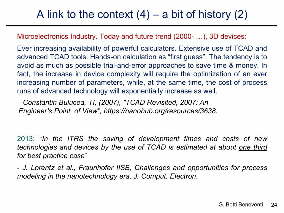
Microelectronics Industry. Today and future trend (2000- …), 3D devices:
Ever increasing availability of powerful calculators. Extensive use of TCAD and
advanced TCAD tools. Hands-on calculation as “first guess”. The tendency is to
avoid as much as possible trial-and-error approaches to save time & money. In
fact, the increase in device complexity will require the optimization of an ever
increasing number of parameters, while, at the same time, the cost of process
runs of advanced technology will exponentially increase as well.
2013: “In the ITRS the saving of development times and costs of new
technologies and devices by the use of TCAD is estimated at about one third
for best practice case”
- J. Lorentz et al., Fraunhofer IISB, Challenges and opportunities for process
modeling in the nanotechnology era, J. Comput. Electron.
- Constantin Bulucea, TI, (2007), "TCAD Revisited, 2007: An
Engineer’s Point of View”, https://nanohub.org/resources/3638.

25 G. Betti Beneventi
A link to the context (5) – TCAD today: applications
More Moore
CMOS logic
Memory
Interconnect,
USA, Asia
More Than Moore
Analog
Power
Image Sensor
Solar
TSV
USA, Asia, Europe
G.E. Moore, “Cramming more
components onto integrated circuits’,
Electronics, 114-117, pp. 1965
T. Ma, “TCAD Present State and Future Challenges”, IEDM 2010
Moore’s law: the number
of transistors in a chip
increase by a factor 2
within 18 or 24 months

26 G. Betti Beneventi
A link to the context (6) – TCAD today: challenges (1)
New materials used in microelectronics technology have increased tremendously
since the 1980s. This brings about two fundamental needs:
1. Validate existing models for new materials, or develop new models, if needed.
2. Calibrate the models to extract parameters of new materials. Material simulation
tools (ab-initio, molecular dynamics) are used to investigate material behavior
and fed the TCAD tools with appropriate material parameters.
27 G. Betti Beneventi
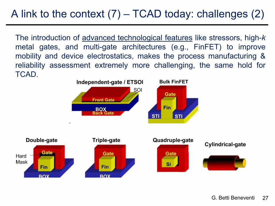
A link to the context (7) – TCAD today: challenges (2)
The introduction of advanced technological features like stressors, high-k
metal gates, and multi-gate architectures (e.g., FinFET) to improve
mobility and device electrostatics, makes the process manufacturing &
reliability assessment extremely more challenging, the same hold for
TCAD.

28 G. Betti Beneventi
TCAD in the semiconductor modeling hierarchy
Drift-Diffusion model Good for devices with gate length > 0.5mm,
but with appropriate advanced add-on features (quantum
models, advanced mobility models) can be extended to
channel lengths of few tens of nm.
Hydrodynamic model Hot-carrier effects, such as velocity overshoot, included
into the model.
Overestimates the velocity at high fields.
Particle-based simulators (Monte-Carlo method) Allows for a proper treatment of the discrete impurity
effects and for electron-electron, electron-ion interactions.
Time consuming.
Quantum models More rigorous but extremely time-consuming. More and more used in these
days owing to the need of exploring the features of extremely scaled devices
and thanks to the availability of ever more powerful computers.
LG< 20 nm
D. Vasileska, (2006), "Introduction to Computational Electronics,“
https://nanohub.org/resources/1501
“TCAD”

29 G. Betti Beneventi
Outline
• Modeling & Simulation
• What is TCAD?
• Why TCAD?
• A link to the context
In this class
• To probe further

30 G. Betti Beneventi
In this class
• Practical TCAD activity using the nowadays most used tool for TCAD in both industry
and research, i.e., Synopsys Sentaurus commercial software (academic license).
• Due their importance in the Electronics Engineering curriculum, we will simulate the
following devices:
– Diode.(simple pn-junction and integrated diode)
– MOSFET (Metal-Oxide-Semiconductor Field-Effect Transistor).
• The concepts used and developed in this class are strictly related to the courses of
semiconductor-device physics provided by the University of Bologna Master curriculum
in Electronics Engineering (Microelectronics & Solid-State-Electronics, Prof. M. Rudan,
and Nanoelectronics, Prof. G. Baccarani).
• In this course, the mathematical and physical foundation needed to understand the
physics behind the simulations will be provided by the lessons given by Prof. M. Rudan.
The laboratory classes only addresses device physics from a phenomenological point
of view to provide an intuitive feeling of device physics when needed, as a support for
the simulations.
• The goal of the course is to provide a general framework that should allow students to
understand the working methodology of TCAD and, more generally, of CAD. Another
goal of the course is provide an intuitive feeling of the physics of the above
semiconductor devices, which are at the heart of each electronic system.

31 G. Betti Beneventi
Outline
• Modeling & Simulation
• What is TCAD?
• Why TCAD?
• A link to the context
• In this class
To probe further
32 G. Betti Beneventi
To probe further (1): websites
• EDA/ECAD
http://en.wikipedia.org/wiki/Electronic_design_automation
– Comprehensive list of tools for electronic design automation
(analog, digital, circuit level, system level, and TCAD as well).
• Synopsis TCAD homepage
http://www.synopsys.com/Tools/TCAD/Pages/default.aspx
• www.nanohub.org (Purdue University)
– Courses, on-line presentations, simulation tools and other useful
free resources about modeling & simulation of semiconductor
devices and materials.

33 G. Betti Beneventi
To probe further (2): scientific literature
IEEE (Institute of Electrical and Electronics Engineers).
Journals
IEEE Transactions on Electron Devices (T-ED)
IEEE Electron Devices Letters (EDL)
Solid-State Electronics
Journal of Computational Electronics
Journal of Applied Physics (JAP)
Applied Physics Letters (APL)
IEEE Transactions on Nanotechnology (T-NANO)
Conferences
The International Conference on Simulation of Semiconductor Processes and Devices
(SISPAD)
The International Electron Device Meeting (IEDM)
International Workshop on Computational Electronics (IWCE)
European Solid-State Device Research Conference (ESSDERC)
Device Research Conference (DRC)