technology - futureelectronics.com image/sii164ctg64.pdf · i2c programming sequence ... panellink...
TRANSCRIPT

®
Technology
SiI 164 PanelLink Transmitter
Data Sheet
Document # SiI-DS-0021-E.doc

SiI 164 PanelLink TransmitterData Sheet
SiI-DS-0021-E ii
Silicon Image, Inc. SiI-DS-0021-E June 2005 Application Information To obtain the most updated Application Notes and other useful information for your design, please visit the Silicon Image web site at www.siliconimage.com or contact your local Silicon Image sales office.
Copyright Notice This manual is copyrighted by Silicon Image, Inc. Do not reproduce, transform to any other format, or send/transmit any part of this documentation without the expressed written permission of Silicon Image, Inc.
Trademark Acknowledgment Silicon Image, the Silicon Image logo, PanelLink® and the PanelLink® Digital logo are registered trademarks of Silicon Image, Inc. TMDSTM is a trademark of Silicon Image, Inc. VESA®, FPDTM are trademarks of the Video Electronics Standards Association. I2C is a trademark of Philips Semiconductor. All other trademarks are the property of their respective holders.
Disclaimer This document provides technical information for the user. Silicon Image, Inc. reserves the right to modify the information in this document as necessary. The customer should make sure that they have the most recent data sheet version. Silicon Image, Inc. holds no responsibility for any errors that may appear in this document. Customers should take appropriate action to ensure their use of the products does not infringe upon any patents. Silicon Image, Inc. respects valid patent rights of third parties and does not infringe upon or assist others to infringe upon such rights.
All information contained herein is subject to change without notice.
Revision History
Revision Date Comment SiI-DS-0021-A 01/99 Full Release SiI-DS-0021-B 03/99 Internal Revision B release SiI-DS-0021-C 04/02 New format. I2C programming and strapping mode
description,TFT mapping and Design Recommendations, pin names ISEL/RST changed to ISEL/RST# and PD to PD#.
SiI-DS-0021-D 09/02 Included Pb-free package. Added De-skew range. Corrected PD# pin number.
SiI-DS-0021-E 06/05 Corrected D1 dimension. Corrected JEDEC code. Included VCC details for power measurement. Added Register Reset values and additional sample programming code.
© 2005 Silicon Image, Inc.

SiI 164 PanelLink Transmitter Data Sheet
iii SiI-DS-0021-E
TABLE OF CONTENTS General Description........................................................................................................................................ 1
Features ...................................................................................................................................................... 1 SiI 164 Pin Diagram ....................................................................................................................................... 1 Functional Description .................................................................................................................................... 2
PanelLink TMDS Digital Core ..................................................................................................................... 2 I2C Interface and Registers......................................................................................................................... 2 Data Capture Logic ..................................................................................................................................... 3
Electrical Specifications .................................................................................................................................. 4 Absolute Maximum Conditions ................................................................................................................... 4 Normal Operating Conditions ..................................................................................................................... 4 Digital I/O Specifications ............................................................................................................................. 4 DC Specifications........................................................................................................................................ 5 AC Specifications ........................................................................................................................................ 6 Input Timing Diagrams ................................................................................................................................ 7
Pin Descriptions.............................................................................................................................................. 9 Input Pins .................................................................................................................................................... 9 Configuration Pins..................................................................................................................................... 10 Input Voltage Reference Pin ..................................................................................................................... 11 Power Management Pins.......................................................................................................................... 11 Differential Signal Data Pins ..................................................................................................................... 11 Reserved Pins........................................................................................................................................... 11 Power and Ground Pins............................................................................................................................ 11
I2C Registers................................................................................................................................................. 12 I2C Register Mapping................................................................................................................................ 12 I2C Register Definitions............................................................................................................................. 13 I2C Slave Interface and Address ............................................................................................................... 15 Data De-skew Feature .............................................................................................................................. 16 Data Latching Modes ................................................................................................................................ 17 I2C Programming Sequence ..................................................................................................................... 18 Enabling Hot Plug Detection Mode........................................................................................................... 18 Non-I2C/Strap Mode Configuration ........................................................................................................... 19
TFT Panel Data Mapping.............................................................................................................................. 21 Design Recommendations ........................................................................................................................... 24
1.5V to 3.3V I2C Bus Level-Shifting .......................................................................................................... 24 Voltage Ripple Regulation......................................................................................................................... 25 Decoupling Capacitors.............................................................................................................................. 26 Series Damping Resistors on Outputs...................................................................................................... 27 Differential Trace Routing ......................................................................................................................... 27
Package Dimensions and Marking Specification ......................................................................................... 29 Ordering Information..................................................................................................................................... 29

SiI 164 PanelLink TransmitterData Sheet
SiI-DS-0021-E iv
LIST OF TABLES
Table 1. Data De-Skew Estimated Values.................................................................................................... 16 Table 2. Sample Programming Sequence for SiI 164 in 12-bit Mode .......................................................... 18 Table 3. Non-I2C/Strap Mode Options .......................................................................................................... 20 Table 4. One Pixel/Clock Input/Output TFT Mode - VESA P&D and FPDI-2 Compliant.............................. 21 Table 5. 24-bit One Pixel/Clock Input with 24-bit Two Pixels/Clock Output TFT Mode................................ 22 Table 6. 18-bit One Pixel/Clock Input with 18-bit Two Pixels/Clock Output TFT Mode................................ 23 Table 7. Recommended Components for Bypass and Decoupling Circuits................................................. 26
LIST OF FIGURES
Figure 1. Pin Diagram for SiI 164 ................................................................................................................... 1 Figure 2. Functional Block Diagram ............................................................................................................... 2 Figure 3. Clock Cycle High/Low Times........................................................................................................... 7 Figure 4. Low Swing Differential Times .......................................................................................................... 7 Figure 5. ISEL/RST# Minimum Timing ........................................................................................................... 7 Figure 6. Input Data Setup/Hold Time to IDCK .............................................................................................. 8 Figure 7. VSYNC, HSYNC and CTL[3:1] Delay Time from DE...................................................................... 8 Figure 8. DE High and Low Times.................................................................................................................. 8 Figure 9. I2C Data Valid Delay (driving Read Cycle data) .............................................................................. 8 Figure 10. I2C Byte Read.............................................................................................................................. 15 Figure 11. I2C Byte Write .............................................................................................................................. 15 Figure 12. SiI 164 Data De-skew Feature Timing ........................................................................................ 16 Figure 13. 12-bit Input Data Latching ........................................................................................................... 17 Figure 14. 24-bit Input Data Latching ........................................................................................................... 17 Figure 15. Non- I2C/Strap Mode Schematic Example .................................................................................. 19 Figure 16. I2C Bus Voltage Level-Shifting using Fairchild NDC7002N ........................................................ 24 Figure 17. I2C Bus Voltage Level Shifting using Philips GTL 2010 .............................................................. 24 Figure 18. Voltage Regulation using TL431 ................................................................................................. 25 Figure 19. Voltage Regulation using LM317 ................................................................................................ 25 Figure 20. Decoupling and Bypass Capacitor Placement............................................................................ 26 Figure 21. Decoupling and Bypass Schematic............................................................................................. 26 Figure 22. Series Input Damping Resistors for Driving Source ................................................................... 27 Figure 23. Example of Incorrect Differential Signal Routing ........................................................................ 27 Figure 24. Example of Correct Differential Signal Routing........................................................................... 28 Figure 25. Differential Trace Routing to DVI Connector(Top Side View) ..................................................... 28 Figure 26. 64-pin TQFP Package Dimensions (JEDEC code MS-026ACD) ............................................... 29

SiI 164 PanelLink Transmitter September 2002 Data Sheet
1 SiI-DS-0021-E
General Description
The SiI 164 transmitter uses PanelLink® Digital technology to support displays ranging from VGA to UXGA resolutions (25 - 165Mpps) in a single link interface. The SiI 164 transmitter has a highly flexible interface with either a 12-bit mode (½ pixel per clock edge) or 24-bit mode 1 pixel per clock edge input for true color (16.7 million) support. In 24-bit mode, the SiI 164 supports single or dual edge clocking. In 12-bit mode, the SiI164 supports dual edge single clocking or single edge dual clocking. The SiI 164 can be programmed though an I2C interface. In addition the SiI 164 also supports Receiver and Hot Plug Detection. PanelLink Digital technology simplifies PC design by resolving many of the system level issues associated with high-speed mixed signal design, providing the system designer with a digital interface solution that is quicker to market and lower in cost.
Features • Scaleable Bandwidth: 25 - 165MHz Flexible • Graphics Controller Interface: 12-bit or 24-bit
mode 1 pixel/clock inputs • Flexible Input Clocking: Single clock single
edge (24-bit), Single clock dual edge (12-/24-bit), Dual clock single edge (12-bit)
• I2C Slave Programming Interface up to 100kHz • Low Voltage Interface: 3.3V with option for 1.0
to 3.0V Low Voltage Signal Mode • Monitor Detection supported through hot plug
and receiver detection • De-skewing Option varies input clock to input
data timing • Low Power: 3.3V operation (120mA max.) and
Power Down mode (1mA max.) • Cable Distance Support: over 5m with twisted
pair and fiber-optics ready • Compliant with DVI 1.0 (DVI is backwards
compliant with VESA® P&DTM and DFP) • Standard and Pb-free packages (see pg 29)
SiI 164 Pin Diagram
VCC
DE
VREF
HSYNC
VSYNC
CTL3/A3/DK3
CTL2/A2/DK2
CTL1/A1/DK1
EDGE/HTPLG
PD#
MSEN
VCC
ISEL/RST#
DSEL/SDA
BSEL/SCL
GNDP
GN
D
PV
CC
1
EX
T_S
WIN
G
AG
ND
TXC
-
TXC
+
AV
CC
TX0-
TX0+
AG
ND
TX1-
TX1+
AV
CC
TX2-
TX2+
VCC
RESERVED
DKEN
D23
D22
D21
D20
D19
D18
D17
D16
D15
D14
D13
D12
GND
PV
CC
2
D11
D10 D
9
D8
D7
D6
IDC
K-
IDC
K+ D5
D4
D3
D2
D1
D0
GN
D
1
2
3
4
5
6
7
8
9
10
11
12
13
14
15
1617181920212223242526272829303132
33
34
35
36
37
38
39
40
41
42
43
44
45
46
47
48
49 50 51 52 53 54 55 56 57 58 59 60 61 62 63 64
SiI 16464-Pin TQFP(Top View)
AG
ND
Figure 1. Pin Diagram for SiI 164

SiI 164 PanelLink Transmitter Data Sheet
SiI-DS-0021-E 2
Functional Description The SiI 164 is a DVI 1.0 compliant PanelLink transmitter in a compact package. It provides 24-bit data Input to allow for panel support up to UXGA resolution. Figure 2 shows the functional blocks of the chip.
Registers&
ConfigurationLogic Block
SC
L
SD
A
PD
ED
GE
/HTP
LG
BS
EL/
SC
LD
SE
L/S
DA
CTL
/A/D
K[3
:1]
I2CSlave
Machine
Data CaptureLogic Block
D[2
3:0]
IDC
K+
IDC
K-
VS
YN
C
HS
YN
C
TXC
+
TX0+
TX1+
TX2+
VREF
DE
MS
EN
PanelLinkDigitalcore
ISE
L/R
ST
EXT_SWING
DK
EN
A[3
:1]
Figure 2. Functional Block Diagram
PanelLink TMDS Digital Core The PanelLink TMDS core encodes video information onto three TMDS differential data lines and the differential clock. The video data is input by the Data Capture Logic Block, as a 12- or 24-bit bus, using one or two clocks with one or two edges per clock. An attached monitor may be sensed using the HTPLG pin or internally with Receiver Sense. This detected state may be output onto the MSEN pin. The device may be powered down using the PD# pin or with an internal register. The SiI 164 is reset using the ISEL/RST# pin. A resistor tied to the EXT_SWING pin is used to control the TMDS swing amplitude.
I2C Interface and Registers The SiI 164 uses a slave I2C interface, capable of running at 100kHz. The slave I2C interface is not 5V tolerant. If the switching levels from the host are not 3.3V, then a voltage level shifter must be used. See Figure 16 and Figure 17 on page 24 for a system diagram.
A connected display may be detected using the DVI Hot Plug signal, attached to the HTPLG pin; or with the Receiver Sense logic internal to the SiI 164. The state of the detection, or an interrupt signal indicating a change of state, may be sent to the MSEN pin. This is useful to the host controller monitoring the SiI 164.

SiI 164 PanelLink Transmitter Data Sheet
3 SiI-DS-0021-E
Data Capture Logic Video data is input to the SiI 164 by way of a 12-bit or 24-bit interface. The functionality of this interface is affected by several of the configuration register settings, as follows.
• BSEL selects between 12-bit and 24-bit input bus widths.
• DSEL selects between single-edge and dual-edge modes for the input clocks.
• EDGE selects between rising and falling edge on the input clocks.
• CLK+ and CLK- provide the one or two clocks required for latching the input data bus.
• The PD# input selects the chip power down mode and allows for disabling of the TMDS outputs.
The ISEL/RST# input resets the HDCP engine and internal registers and is asserted after power up and receipt of a stable input pixel clock.
SiI 164 PanelLink Transmitter Data Sheet
SiI-DS-0021-E 4
Electrical Specifications
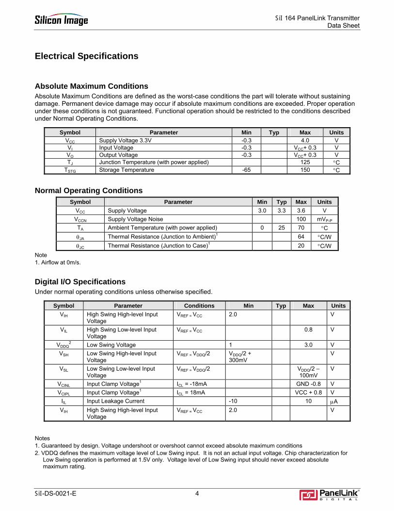
Absolute Maximum Conditions Absolute Maximum Conditions are defined as the worst-case conditions the part will tolerate without sustaining damage. Permanent device damage may occur if absolute maximum conditions are exceeded. Proper operation under these conditions is not guaranteed. Functional operation should be restricted to the conditions described under Normal Operating Conditions.
Symbol Parameter Min Typ Max Units VCC Supply Voltage 3.3V -0.3 4.0 V VI Input Voltage -0.3 VCC+ 0.3 V VO Output Voltage -0.3 VCC+ 0.3 V TJ Junction Temperature (with power applied) 125 °C
TSTG Storage Temperature -65 150 °C
Normal Operating Conditions Symbol Parameter Min Typ Max Units
VCC Supply Voltage 3.0 3.3 3.6 V VCCN Supply Voltage Noise 100 mVP-P TA Ambient Temperature (with power applied) 0 25 70 °C θJA Thermal Resistance (Junction to Ambient)1 64 °C/W θJC Thermal Resistance (Junction to Case)1 20 °C/W
Note 1. Airflow at 0m/s.
Digital I/O Specifications Under normal operating conditions unless otherwise specified.
Symbol Parameter Conditions Min Typ Max Units VIH High Swing High-level Input
Voltage VREF = VCC 2.0 V
VIL High Swing Low-level Input Voltage
VREF = VCC 0.8 V
VDDQ2 Low Swing Voltage 1 3.0 V
VSH Low Swing High-level Input Voltage
VREF = VDDQ/2 VDDQ/2 + 300mV
V
VSL Low Swing Low-level Input Voltage
VREF = VDDQ/2 VDDQ/2 – 100mV
V
VCINL Input Clamp Voltage1 ICL = -18mA GND -0.8 V VCIPL Input Clamp Voltage1 ICL = 18mA VCC + 0.8 V
IIL Input Leakage Current -10 10 µA VIH High Swing High-level Input
Voltage VREF = VCC 2.0 V
Notes 1. Guaranteed by design. Voltage undershoot or overshoot cannot exceed absolute maximum conditions 2. VDDQ defines the maximum voltage level of Low Swing input. It is not an actual input voltage. Chip characterization for Low Swing operation is performed at 1.5V only. Voltage level of Low Swing input should never exceed absolute maximum rating.

SiI 164 PanelLink Transmitter Data Sheet
5 SiI-DS-0021-E
DC Specifications Under normal operating conditions unless otherwise specified.
Symbol Parameter Conditions Min Typ Max Units VOD Differential Voltage Single ended
peak to peak amplitude RLOAD = 50Ω, REXT_SWING = 510Ω 510 550 590 mV
VDOH Differential High-level Output AVCC V Voltage1
IDOS Differential Output Short Circuit Current1
VOUT = 0 V 5 µA
IPD# Power-down Current2 0.2 1.0 mA ICCT Transmitter Supply Current IDCK= 165 MHz, 1-pixel/clock
mode, REXT_SWING = 510Ω, Worst Case Pattern3
854 1205 mA
Notes 1. Guaranteed by design. 2. Assumes all inputs to the transmitter are not toggling. 3. Black and white checkerboard pattern, each checker is one pixel wide. 4. Measurement taken at VCC = 3.30V. 5. Measurement taken at VCC = 3.60V.

SiI 164 PanelLink Transmitter Data Sheet
SiI-DS-0021-E 6
AC Specifications Under normal operating conditions unless otherwise specified.
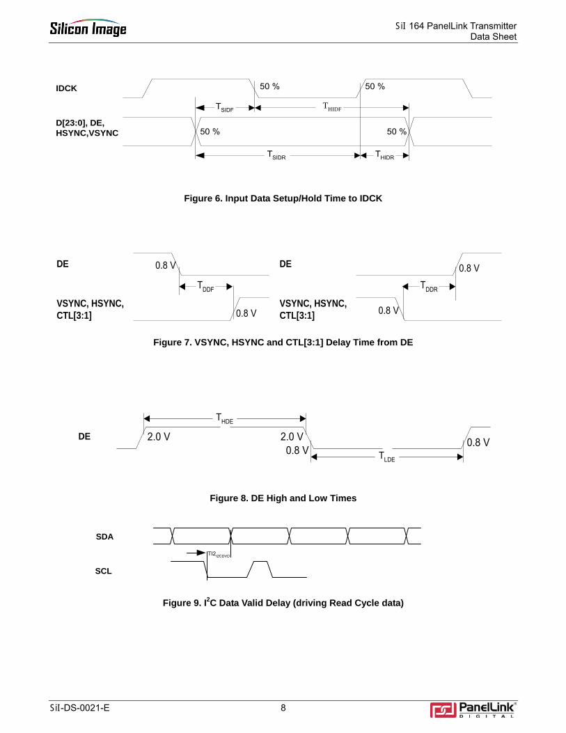
Symbol Parameter Conditions Min Typ Max Units Figure TCIP IDCK Period, 1-pixel/clock 6 40 ns Figure 3 FCIP IDCK Frequency, 1-pixel/clock 25 165 MHz TCIH IDCK High Time at 165MHz 2.0 ns Figure 3 TCIL IDCK Low Time at 165MHz 2.0 ns Figure 3 TIJIT Worst Case IDCK Clock Jitter2,3 2 ns TSIDF Data, DE, VSYNC, HSYNC
Setup Time to IDCK falling edge (Default De-skew Setting)
Single Edge (DSEL = 0, EDGE = 0)
1.0 ns Figure 6
THIDF Data, DE, VSYNC, HSYNC Hold Time from IDCK falling edge (Default De-skew Setting)
Single Edge (DSEL = 0, EDGE = 0)
0.9 ns Figure 6
TSIDR Data, DE, VSYNC, HSYNC Setup Time to IDCK rising edge1
(Default De-skew Setting)
Single Edge (DSEL = 0, EDGE = 1)
1.0 ns Figure 6
THIDR Data, DE, VSYNC, HSYNC Hold Time from IDCK rising edge1
(Default De-skew Setting)
Single Edge (DSEL = 0, EDGE = 1)
0.9 ns Figure 6
TSID Data, DE, VSYNC, HSYNC Setup Time to IDCK falling/rising edge1
(Default De-skew Setting)
Dual Edge (DSEL = 1, BSEL = 0)
0.6 ns
THID Data, DE, VSYNC, HSYNC Hold Time from IDCK falling/rising edge1
(Default De-skew Setting)
Dual Edge (DSEL = 1, BSEL = 0)
1.3 ns
TDDF VSYNC, HSYNC Delay from DE falling edge1
1TCIP ns Figure 7
TDDR VSYNC, HSYNC Delay to DE rising edge1 1TCIP ns Figure 7 THDE DE high time1 8191TCIP ns Figure 8 TLDE DE low time1 128TCIP ns Figure 8 TSTEP De-skew step size increment DKEN = 0b1 260 ps TRESET Duration of RESET signal Low required for
valid Reset 10 µs Figure 5
CL = 10pf 700 ns TI2CDVD SDA Data Valid Delay from SCL high to low transition3 CL = 400pf 2000 ns
Figure 9
SHLT Differential Swing High-to-Low Transition Time
RLOAD = 50Ω, REXT_SWING = 510Ω
170 200 230 ps Figure 4
SLHT Differential Swing Low-to-High Transition Time
RLOAD = 50Ω, REXT_SWING = 510Ω
170 200 230 ps Figure 4
Notes 1. Guaranteed by design. 2. Actual jitter tolerance may be higher depending on the frequency of the jitter. 3. All Standard mode I2C (100kHz) timing requirements are guaranteed by design. Fast mode I2C (400kHz) timing requirements are guaranteed at 10pf loading.
SiI 164 PanelLink Transmitter Data Sheet
7 SiI-DS-0021-E
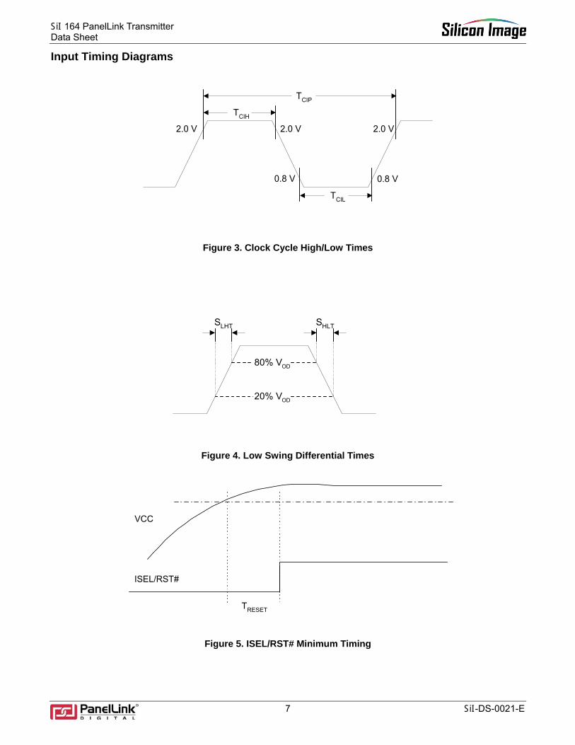
Input Timing Diagrams
TCIH
TCIL
TCIP
2.0 V
0.8 V0.8 V
2.0 V 2.0 V
Figure 3. Clock Cycle High/Low Times
Figure 4. Low Swing Differential Times
ISEL/RST#
VCC
TRESET
Figure 5. ISEL/RST# Minimum Timing
SLHT
20% VOD
80% VOD
SHLT
SiI 164 PanelLink Transmitter Data Sheet
SiI-DS-0021-E 8
Figure 6. Input Data Setup/Hold Time to IDCK
Figure 7. VSYNC, HSYNC and CTL[3:1] Delay Time from DE
DE
TLDE
THDE
0.8 V2.0 V0.8 V
2.0 V
Figure 8. DE High and Low Times
Figure 9. I2C Data Valid Delay (driving Read Cycle data)
D[23:0], DE,HSYNC,VSYNC
IDCK
TSIDF THIDF
TSIDR THIDR
50 %
50 % 50 %
50 %
TDDRTDDF
DE
VSYNC, HSYNC,CTL[3:1]
0.8 V
0.8 V 0.8 V
0.8 VDE
VSYNC, HSYNC,CTL[3:1]
SCL
TI2I2CDVD
SDA

SiI 164 PanelLink Transmitter Data Sheet
9 SiI-DS-0021-E
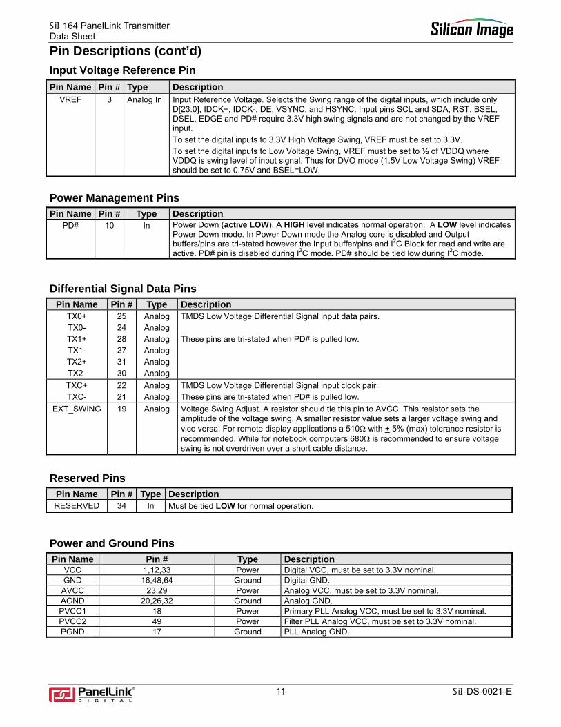
Pin Descriptions
Input Pins Pin Name Pin # Type Description
D[23:12]
36-47 In
Top half of 24-bit pixel bus. When BSEL = HIGH, this bus inputs the top half of the 24-bit pixel bus. When BSEL = LOW, these bits are not used to input pixel data. In this mode, the state of D[23:16] is input to the I2C register CFG. This allows 8-bits of user configuration data to be read by the graphics controller through the I2C interface (see I2C register definition). When not used D[23:16] should be tied to ground. D[15:12] are reserved for SiI use only and should be tied to GND.
D[11:0] 50-55,
58-63
In
Bottom half of 24-bit pixel bus / 12-bit pixel bus input. When BSEL = HIGH, this bus inputs the bottom half of the 24-bit pixel bus. When BSEL = LOW, this bus inputs ½ a pixel (12-bits) at every latch edge (both falling and/or rising) of the clock.
IDCK+ 57 In Input Data Clock +. This clock is used for all input modes. IDCK- 56 In Input Data Clock –. This clock is only used in 12-bit mode when dual edge clocking is turned
off (DSEL = LOW). It is used to provide the ODD latching edges for dual clock single edge. If BSEL = HIGH or DSEL = HIGH, this pin is unused and should be tied to GND.
DE 2 In Input Data Enable. This signal qualifies the active data area. DE is always required by the transmitter and must be high during active display time and low during blanking time.
HSYNC 4 In Horizontal Sync input control Signal VSYNC 5 In Vertical Sync input control signal.
CTL1/A1/DK1 CTL2/A2/DK2 CTL3/A3/DK3
8 7 6
In The use of these multi-function inputs depends on the settings of ISEL/RST# and DKEN. These inputs are regular high-swing 3.3V CMOS level inputs. These pins contain weak pull-down resistors so that if left unconnected, they will be LOW. When ISEL/RST# = LOW, DKEN = LOW General Purpose Input CTL[3:1] pins are active, for backward compatibility. These pins must be used to send DC signals only during the blanking time. When ISEL/RST# = LOW, DKEN = HIGH DK[3:1] are active, these inputs are used to select the De-skewing setting for the input bus. When ISEL/RST# = HIGH, DKEN = HIGH A[3:1] are active, these bits are used to set the lower 3 bits of the I2C device address.
SiI 164 PanelLink Transmitter Data Sheet
SiI-DS-0021-E 10
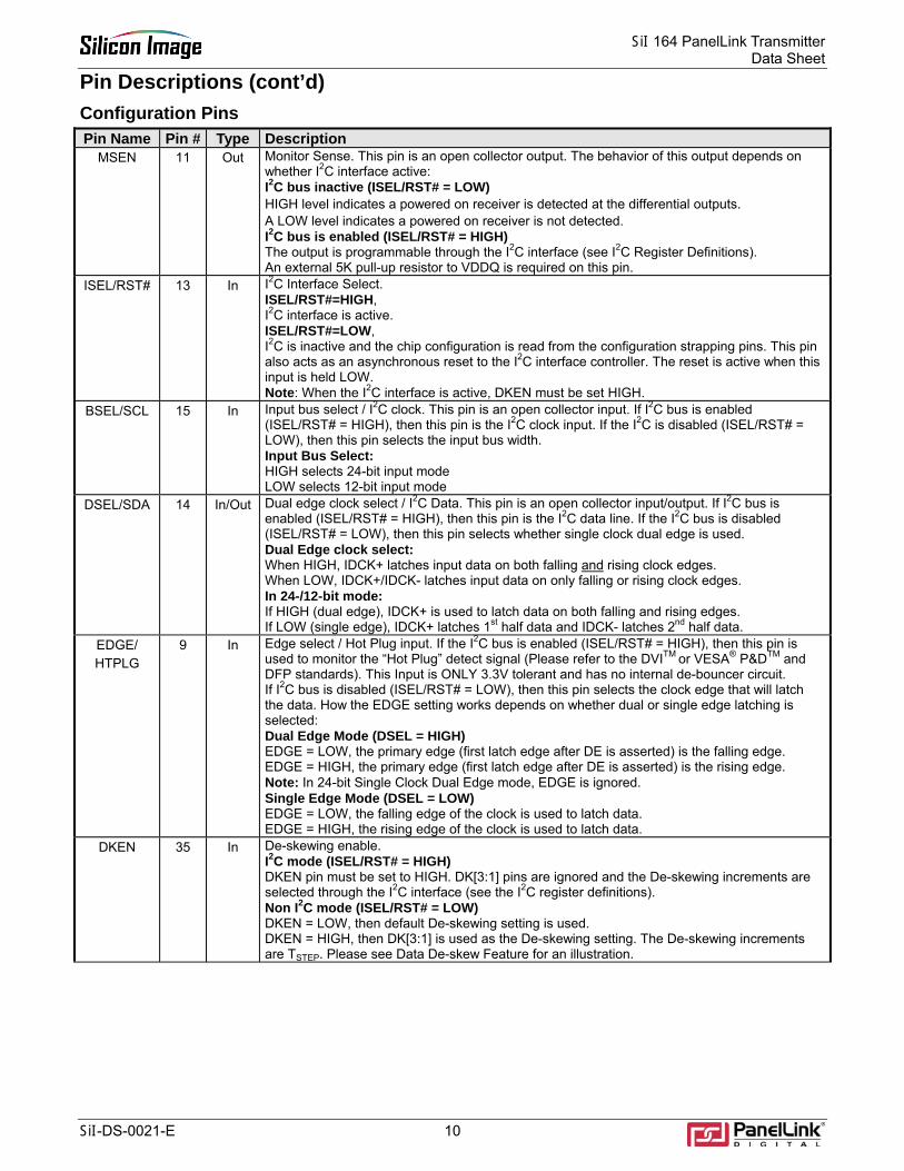
Pin Descriptions (cont’d) Configuration Pins Pin Name Pin # Type Description
MSEN 11 Out Monitor Sense. This pin is an open collector output. The behavior of this output depends on whether I2C interface active: I2C bus inactive (ISEL/RST# = LOW) HIGH level indicates a powered on receiver is detected at the differential outputs. A LOW level indicates a powered on receiver is not detected. I2C bus is enabled (ISEL/RST# = HIGH) The output is programmable through the I2C interface (see I2C Register Definitions). An external 5K pull-up resistor to VDDQ is required on this pin.
ISEL/RST# 13 In I2C Interface Select. ISEL/RST#=HIGH, I2C interface is active. ISEL/RST#=LOW, I2C is inactive and the chip configuration is read from the configuration strapping pins. This pin also acts as an asynchronous reset to the I2C interface controller. The reset is active when this input is held LOW. Note: When the I2C interface is active, DKEN must be set HIGH.
BSEL/SCL 15 In Input bus select / I2C clock. This pin is an open collector input. If I2C bus is enabled (ISEL/RST# = HIGH), then this pin is the I2C clock input. If the I2C is disabled (ISEL/RST# = LOW), then this pin selects the input bus width. Input Bus Select: HIGH selects 24-bit input mode LOW selects 12-bit input mode
DSEL/SDA 14 In/Out Dual edge clock select / I2C Data. This pin is an open collector input/output. If I2C bus is enabled (ISEL/RST# = HIGH), then this pin is the I2C data line. If the I2C bus is disabled (ISEL/RST# = LOW), then this pin selects whether single clock dual edge is used. Dual Edge clock select: When HIGH, IDCK+ latches input data on both falling and rising clock edges. When LOW, IDCK+/IDCK- latches input data on only falling or rising clock edges. In 24-/12-bit mode: If HIGH (dual edge), IDCK+ is used to latch data on both falling and rising edges. If LOW (single edge), IDCK+ latches 1st half data and IDCK- latches 2nd half data.
EDGE/ HTPLG
9 In Edge select / Hot Plug input. If the I2C bus is enabled (ISEL/RST# = HIGH), then this pin is used to monitor the “Hot Plug” detect signal (Please refer to the DVITM or VESA® P&DTM and DFP standards). This Input is ONLY 3.3V tolerant and has no internal de-bouncer circuit. If I2C bus is disabled (ISEL/RST# = LOW), then this pin selects the clock edge that will latch the data. How the EDGE setting works depends on whether dual or single edge latching is selected: Dual Edge Mode (DSEL = HIGH) EDGE = LOW, the primary edge (first latch edge after DE is asserted) is the falling edge. EDGE = HIGH, the primary edge (first latch edge after DE is asserted) is the rising edge. Note: In 24-bit Single Clock Dual Edge mode, EDGE is ignored. Single Edge Mode (DSEL = LOW) EDGE = LOW, the falling edge of the clock is used to latch data. EDGE = HIGH, the rising edge of the clock is used to latch data.
DKEN 35 In De-skewing enable. I2C mode (ISEL/RST# = HIGH) DKEN pin must be set to HIGH. DK[3:1] pins are ignored and the De-skewing increments are selected through the I2C interface (see the I2C register definitions). Non I2C mode (ISEL/RST# = LOW) DKEN = LOW, then default De-skewing setting is used. DKEN = HIGH, then DK[3:1] is used as the De-skewing setting. The De-skewing increments are TSTEP. Please see Data De-skew Feature for an illustration.
SiI 164 PanelLink Transmitter Data Sheet
11 SiI-DS-0021-E
Pin Descriptions (cont’d) Input Voltage Reference Pin Pin Name Pin # Type Description
VREF 3 Analog In Input Reference Voltage. Selects the Swing range of the digital inputs, which include only D[23:0], IDCK+, IDCK-, DE, VSYNC, and HSYNC. Input pins SCL and SDA, RST, BSEL, DSEL, EDGE and PD# require 3.3V high swing signals and are not changed by the VREF input. To set the digital inputs to 3.3V High Voltage Swing, VREF must be set to 3.3V. To set the digital inputs to Low Voltage Swing, VREF must be set to ½ of VDDQ where VDDQ is swing level of input signal. Thus for DVO mode (1.5V Low Voltage Swing) VREF should be set to 0.75V and BSEL=LOW.
Power Management Pins Pin Name Pin # Type Description
PD# 10 In Power Down (active LOW). A HIGH level indicates normal operation. A LOW level indicates Power Down mode. In Power Down mode the Analog core is disabled and Output buffers/pins are tri-stated however the Input buffer/pins and I2C Block for read and write are active. PD# pin is disabled during I2C mode. PD# should be tied low during I2C mode.
Differential Signal Data Pins Pin Name Pin # Type Description
TX0+ TX0- TX1+ TX1- TX2+ TX2-
25 24 28 27 31 30
Analog Analog Analog Analog Analog Analog
TMDS Low Voltage Differential Signal input data pairs. These pins are tri-stated when PD# is pulled low.
TXC+ TXC-
22 21
Analog Analog
TMDS Low Voltage Differential Signal input clock pair. These pins are tri-stated when PD# is pulled low.
EXT_SWING 19 Analog Voltage Swing Adjust. A resistor should tie this pin to AVCC. This resistor sets the amplitude of the voltage swing. A smaller resistor value sets a larger voltage swing and vice versa. For remote display applications a 510Ω with + 5% (max) tolerance resistor is recommended. While for notebook computers 680Ω is recommended to ensure voltage swing is not overdriven over a short cable distance.
Reserved Pins Pin Name Pin # Type Description RESERVED 34 In Must be tied LOW for normal operation.
Power and Ground Pins Pin Name Pin # Type Description
VCC 1,12,33 Power Digital VCC, must be set to 3.3V nominal. GND 16,48,64 Ground Digital GND. AVCC 23,29 Power Analog VCC, must be set to 3.3V nominal. AGND 20,26,32 Ground Analog GND. PVCC1 18 Power Primary PLL Analog VCC, must be set to 3.3V nominal. PVCC2 49 Power Filter PLL Analog VCC, must be set to 3.3V nominal. PGND 17 Ground PLL Analog GND.

SiI 164 PanelLink Transmitter Data Sheet
SiI-DS-0021-E 12
I2C Registers
I2C Register Mapping Addr Reset
Value Bit 7 Bit 6 Bit 5 Bit 4 Bit 3 Bit 2 Bit 1 Bit 0
0x00 0x01 VND_IDL
0x01 0x00 VND_IDH
0x02 0x06 DEV_IDL
0x03 0x00 DEV_IDH
0x04 0x00 DEV_REV
0x05 0x00 RSVD
0x06 0x19 FRQ_LOW
0x07 0x64 FRQ_HIGH
0x08 000
RSVD VEN HEN DSEL BSEL EDGE PD#
0x09 000 00
RSVD MSEL TSEL RSEN HTPLG MDI
0x0A 0x90 DK[3:1] DKEN CTL[3:1] RSVD
0x0B
CFG[7:0]
0x0C 0
SCNT RSVD PLLF[3:0] PFEN
0x0D 0x80 RSVD
0x0E 0x00 RSVD
0x0F 0x00 RSVD
Notes 1. All values are Bit 7 [MSB] and Bit 0 [LSB]. 2. Bits and registers bold like this are read only. All others are Read/Write. 3. Bits and registers in italics and bold like this are undefined after RESET, although they are accessible by read or write. 4. RSVD is a reserved register or bit field. It is available for future use by Silicon Image. All RSVD fields are read-only and
are not affected by data written to them. 5. 0x0C is also called the VDJK Register. Default setting for the VDJK register 0x0C is 0x89, which is optimum for most
applications. I2C Reset values are shown in the column at the left of the table. Bits or registers which have no default value after power-on, or which have no defined value after RESET, are shown with the symbol in the table. All registers Hexadecimal values use a prefix of ‘0x’. Binary values use a prefix of ‘0b’. To enable the device, registers 0x08, 0x09, 0x0A and 0x0C must be programmed. A sample programming sequence is listed on page 18 for 12-bit mode.
SiI 164 PanelLink Transmitter Data Sheet
13 SiI-DS-0021-E
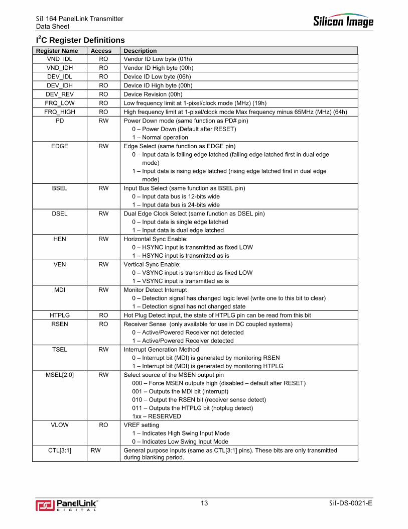
I2C Register Definitions Register Name Access Description
VND_IDL RO Vendor ID Low byte (01h) VND_IDH RO Vendor ID High byte (00h) DEV_IDL RO Device ID Low byte (06h) DEV_IDH RO Device ID High byte (00h) DEV_REV RO Device Revision (00h) FRQ_LOW RO Low frequency limit at 1-pixel/clock mode (MHz) (19h) FRQ_HIGH RO High frequency limit at 1-pixel/clock mode Max frequency minus 65MHz (MHz) (64h)
PD RW Power Down mode (same function as PD# pin) 0 – Power Down (Default after RESET) 1 – Normal operation
EDGE RW Edge Select (same function as EDGE pin) 0 – Input data is falling edge latched (falling edge latched first in dual edge mode) 1 – Input data is rising edge latched (rising edge latched first in dual edge mode)
BSEL RW Input Bus Select (same function as BSEL pin) 0 – Input data bus is 12-bits wide 1 – Input data bus is 24-bits wide
DSEL RW Dual Edge Clock Select (same function as DSEL pin) 0 – Input data is single edge latched 1 – Input data is dual edge latched
HEN RW Horizontal Sync Enable: 0 – HSYNC input is transmitted as fixed LOW 1 – HSYNC input is transmitted as is
VEN RW Vertical Sync Enable: 0 – VSYNC input is transmitted as fixed LOW 1 – VSYNC input is transmitted as is
MDI RW Monitor Detect Interrupt 0 – Detection signal has changed logic level (write one to this bit to clear) 1 – Detection signal has not changed state
HTPLG RO Hot Plug Detect input, the state of HTPLG pin can be read from this bit RSEN RO Receiver Sense (only available for use in DC coupled systems)
0 – Active/Powered Receiver not detected 1 – Active/Powered Receiver detected
TSEL RW Interrupt Generation Method 0 – Interrupt bit (MDI) is generated by monitoring RSEN 1 – Interrupt bit (MDI) is generated by monitoring HTPLG
MSEL[2:0] RW Select source of the MSEN output pin 000 – Force MSEN outputs high (disabled – default after RESET) 001 – Outputs the MDI bit (interrupt) 010 – Output the RSEN bit (receiver sense detect) 011 – Outputs the HTPLG bit (hotplug detect) 1xx – RESERVED
VLOW RO VREF setting 1 – Indicates High Swing Input Mode 0 – Indicates Low Swing Input Mode
CTL[3:1] RW General purpose inputs (same as CTL[3:1] pins). These bits are only transmitted during blanking period.

SiI 164 PanelLink Transmitter Data Sheet
SiI-DS-0021-E 14
I2C Register Definitions (cont’d) Register Name Access Description
CFG[7:0] RO Contains state of inputs D[23:16]. These pins can be used to provide user selectable configuration data through the I2C bus. Only available in 12-bit mode
PFEN RW PLL Filter Enable in the VDJK Register 0x0C. 1 – To enable PLL Filter (recommended setting) 0 – To disable PLL Filter
PLLF[3:1] RW Set characteristics of PLL filter in VDJK Register 0x0C. 100 – Recommended value All other values are not recommended.
SCNT RW SYNC Continuous 1 – To enable (recommended setting) 0 – To disable
DK[3:1] RW De-skewing Setting. Increment 260psec. 000 – 1 step -> minimum setup / maximum hold 001 – 2 step 010 – 3 step 011 – 4 step 100 – 5 step -> default (recommended setting) 101 – 6 step 110 – 7 step 111 – 8 step -> maximum setup / minimum hold Please see Data De-Skew Feature for an illustration
DKEN RW De-skewing Enable through DK[3:1] bits. When DKEN pin is HIGH via pin or set to 1, then De-skew is enabled. When set to 0 De-skew is disabled. Please see Data De-skew Feature on page 16 for an illustration.

SiI 164 PanelLink Transmitter Data Sheet
15 SiI-DS-0021-E
I2C Slave Interface and Address The SiI 164 slave state machine does not require an internal clock and support only byte read and write. Page mode is not supported. The 7-bit binary address of the I2C machine is “0111 A3A2A1R” where R =1 sets a read operation while R=0 sets a write operation. Please see Figure 10 for a Byte Read operation and Figure 11 for a byte write operation. For more detailed information on I2C protocols please refer to I2C Bus Specification version 2.1 available from Philips Semiconductors Inc. When ISEL/RST# = HIGH and DKEN = HIGH, pins 6,7,8 functions as A[3:1]. Each pin can be set to HIGH or LOW to select a desired I2C address for the SiI 164. To set the SiI 164 to 0x72, tie pin 7 and 6 to ground and pull pin 8 to VCC via 2.2K resistor. The recommended setting is to tie pins 6,7 and 8 to ground to set “000” or address 0x70 in I2C mode .
S A3
A2
A1
ACK
S A3
A2
A1
ACK
ACK
P
SlaveAddress Register Address Slave
Address
Data
Stop
Star
t
Star
t
Bus Activity :SiI 164
Bus Activity :Master
SDA Line
Figure 10. I2C Byte Read
S A3
A2
A1
ACK
ACK
P
SlaveAddress Address Data
Stop
Star
t
Bus Activity :SiI 164
Bus Activity :Master
SDA Line
ACK
Figure 11. I2C Byte Write
SiI 164 PanelLink Transmitter Data Sheet
SiI-DS-0021-E 16
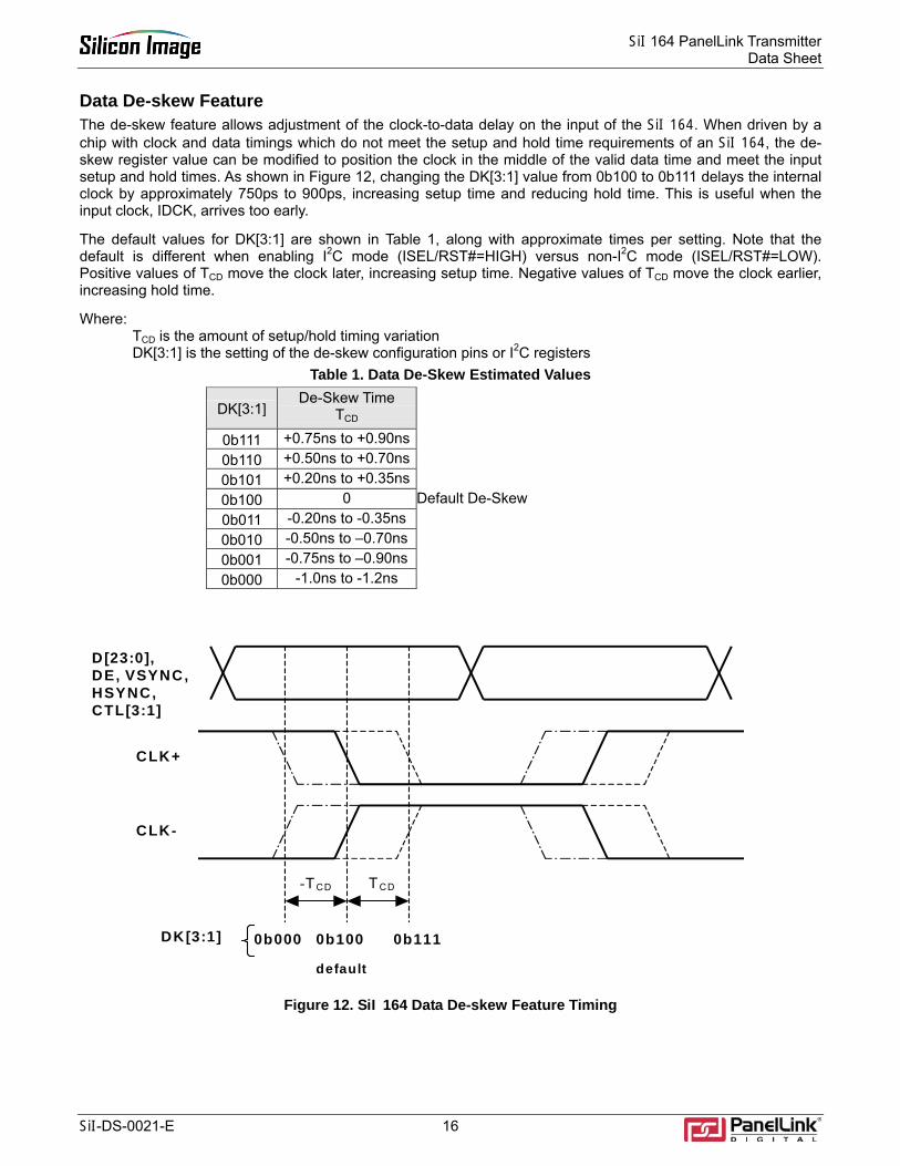
Data De-skew Feature The de-skew feature allows adjustment of the clock-to-data delay on the input of the SiI 164. When driven by a chip with clock and data timings which do not meet the setup and hold time requirements of an SiI 164, the de-skew register value can be modified to position the clock in the middle of the valid data time and meet the input setup and hold times. As shown in Figure 12, changing the DK[3:1] value from 0b100 to 0b111 delays the internal clock by approximately 750ps to 900ps, increasing setup time and reducing hold time. This is useful when the input clock, IDCK, arrives too early.
The default values for DK[3:1] are shown in Table 1, along with approximate times per setting. Note that the default is different when enabling I2C mode (ISEL/RST#=HIGH) versus non-I2C mode (ISEL/RST#=LOW). Positive values of TCD move the clock later, increasing setup time. Negative values of TCD move the clock earlier, increasing hold time.
Where: TCD is the amount of setup/hold timing variation DK[3:1] is the setting of the de-skew configuration pins or I2C registers
Table 1. Data De-Skew Estimated Values
DK[3:1] De-Skew Time
TCD
0b111 +0.75ns to +0.90ns 0b110 +0.50ns to +0.70ns 0b101 +0.20ns to +0.35ns 0b100 0 Default De-Skew 0b011 -0.20ns to -0.35ns 0b010 -0.50ns to –0.70ns 0b001 -0.75ns to –0.90ns 0b000 -1.0ns to -1.2ns
T CD
CLK+
CLK-
DK[3:1] 0b000 0b100 0b111
D[23:0], DE, VSYNC, HSYNC, CTL[3:1]
-T CD
default
Figure 12. SiI 164 Data De-skew Feature Timing
SiI 164 PanelLink Transmitter Data Sheet
17 SiI-DS-0021-E
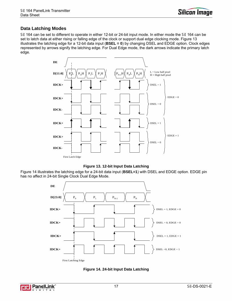
Data Latching Modes SiI 164 can be set to different to operate in either 12-bit or 24-bit input mode. In either mode the SiI 164 can be set to latch data at either rising or falling edge of the clock or support dual edge clocking mode. Figure 13 illustrates the latching edge for a 12-bit data input (BSEL = 0) by changing DSEL and EDGE option. Clock edges represented by arrows signify the latching edge. For Dual Edge mode, the dark arrows indicate the primary latch edge.
P0L POH
IDCK+
D[11:0] P1L P1H PN-1H PNL PNH
DE
IDCK+
IDCK-
IDCK+
IDCK+
IDCK-
DSEL = 1
DSEL = 0
DSEL = 1
DSEL = 0
EDGE = 1
EDGE = 0
L = Low half pixelH = High half pixel
First Latch Edge
Figure 13. 12-bit Input Data Latching Figure 14 illustrates the latching edge for a 24-bit data input (BSEL=1) with DSEL and EDGE option. EDGE pin has no affect in 24-bit Single Clock Dual Edge Mode.
First Latching Edge
P0D[23:0] P1 PN-1 PN
DE
DSEL = 1, EDGE = 0
DSEL = 1, EDGE = 1IDCK+
IDCK+ DSEL =0, EDGE = 1
IDCK+ DSEL = 0, EDGE = 0
IDCK+
Figure 14. 24-bit Input Data Latching

SiI 164 PanelLink Transmitter Data Sheet
SiI-DS-0021-E 18
I2C Programming Sequence To program the SiI 164 in data latched on 12-bit mode Dual Edge Clock with Primary Edge as the rising edge or falling edge, De-skew enabled with Hotplug based monitor detection use the following sample programming sequence listed in Table 2. It is important to note that the suggested I2C address for SiI 164 be set to 0x70 by tying pins A1, A2 and A3 to ground.
Table 2. Sample Programming Sequence for SiI 164 in 12-bit Mode Register(Hex) Value(Hex) Description
0x08 Setting 1: 0x30
Setting 2: 0x32
Setting 1: Enable HEN, VEN, 1st data latched on falling edge with PD low until all registers are programmed.
Setting 2: Enable HEN, VEN, 1st data latched on rising edge with PD low until all registers are programmed.
0x09 0x30 Monitor detection mode via Hotplug input.
0x0A 0x90 De-skew enabled with default 100 value. CTL is not used.
0x0C 0x89 SCNT, PLL Filter Enable and PLL Bandwidth Filter set to default.
0x08 Setting 1: 0x31
Setting 2: 0x33
Setting 1: Recover from Power Down mode and enable output.
Setting 2: Recover from Power Down mode and enable output.
Enabling Hot Plug Detection Mode As documented in the VESA Digital Flat Panel Standard, all monitors are required to support Hot Plug Detection but support is optional for the host. The SiI 164 supports the Hot Plug Detect feature. In I2C mode, pin 9 functions as HTPLG input. It should be noted that the HTPLG pin on the SiI 164 is only 3.3V tolerant therefore HTPLG voltage level from the DVI connector should be level shifted or clamped at 3.3V.
When the voltage level at the HTPLG pin is 3.3V, the HTPLG bit will be set to 1. To output the HTPLG bit via the MSEN pin, register MSEL[2:0] should be programmed to 0b011.
The SiI 164 can also be programmed to enable the Hot Plug Detection Mode via the Receiver Sense function. In this mode, HTPLG pin is not required. By programming MSEL[2:0] to 0b010, SiI 164 will output the RSEN=1 bit though the MSEN pin when the SiI 164 is connected to a powered receiver.
SiI 164 PanelLink Transmitter Data Sheet
19 SiI-DS-0021-E
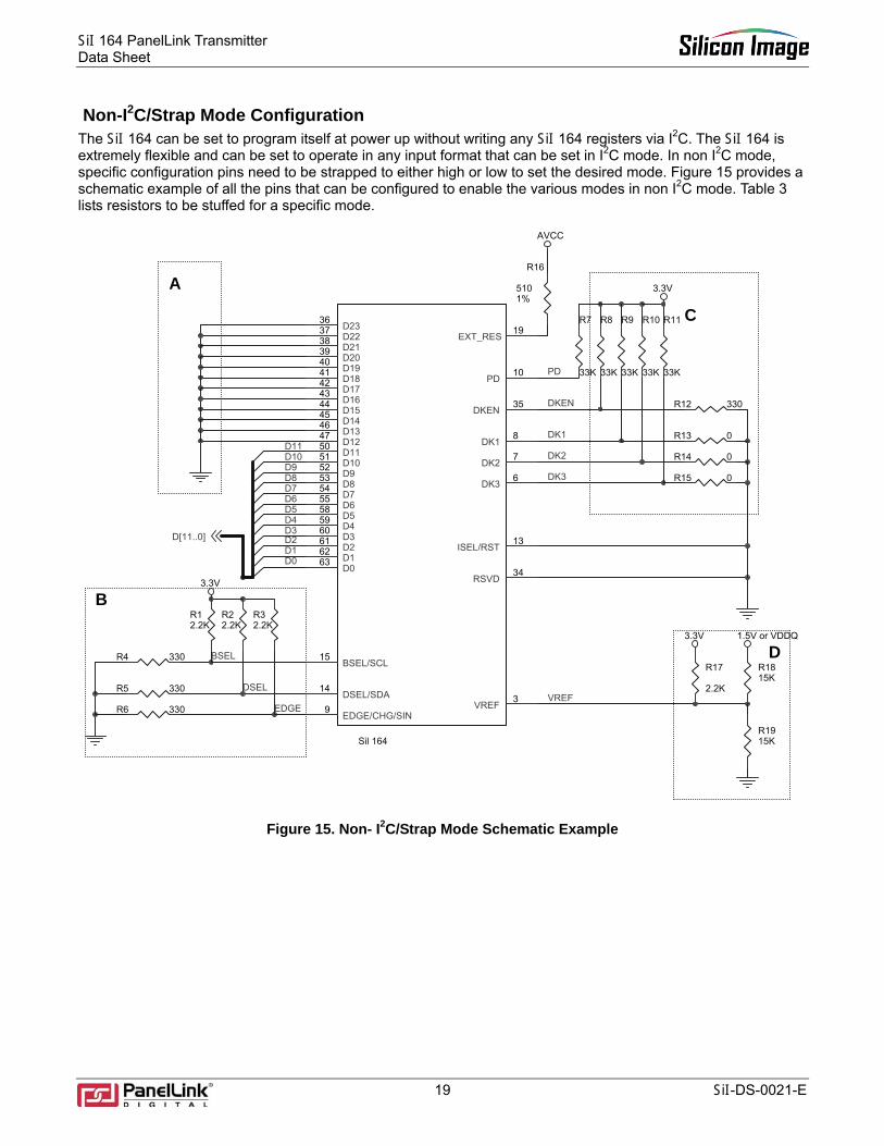
Non-I2C/Strap Mode Configuration The SiI 164 can be set to program itself at power up without writing any SiI 164 registers via I2C. The SiI 164 is extremely flexible and can be set to operate in any input format that can be set in I2C mode. In non I2C mode, specific configuration pins need to be strapped to either high or low to set the desired mode. Figure 15 provides a schematic example of all the pins that can be configured to enable the various modes in non I2C mode. Table 3 lists resistors to be stuffed for a specific mode.
D4
R1815K
3.3V
R10
33K
BSEL
D6
R11
33K
3.3V
R6 330 EDGE
D2
B
DKEN
A
DK1
R8
33K
R22.2K
R15 0
R32.2K
R12 330
D[11..0]
1.5V or VDDQ
D10
R17
2.2K
D8
R14 0
D1
D7
C
R4 330
AVCC
R13 0
D9DK3
DK2
D0
VREF
R1915K
R16
5101%
Sil 164
3
6
7
8
9
10
13
14
15
19
34
35
363738394041424344454647505152535455585960616263
VREF
DK3
DK2
DK1
EDGE/CHG/SIN
PD
ISEL/RST
DSEL/SDA
BSEL/SCL
EXT_RES
RSVD
DKEN
D23D22D21D20D19D18D17D16D15D14D13D12D11D10D9D8D7D6D5D4D3D2D1D0
D5
PD
R12.2K
3.3V
D
D11
R9
33K
DSEL
D3
R7
33K
R5 330
Figure 15. Non- I2C/Strap Mode Schematic Example

SiI 164 PanelLink Transmitter Data Sheet
SiI-DS-0021-E 20
Non-I2C/Strap Mode Configuration (cont’d) ISEL/RST# and RSVD pins must always be tied to ground for strap or non- I2C mode. PD# must be tied high or the SiI 164 will still be in Power Down mode when VCC is applied.
In Figure 15 Block A corresponds to the upper 12-bits (D [23:12]) of the SiI 164. When not in use, they should always be tied to ground. Block B controls the Input Bus data width, Dual Edge Clock Select and Edge Select. IDCK- is only used in 12-bit mode. In 24-bit mode or Dual Edge Clock select IDCK- should be tied to ground. Block C controls the De-skew options. Block D determines the input voltage level swing. A full description of each pin can be found in the Pin Description section of this document.
Table 3. Non-I2C/Strap Mode Options MODE BLOCK A BLOCK B BLOCK C BLOCK D
1. 24-bit1 2. Single Clock 3. Dual Edge 4. Falling Edge
latching 1st pixel 5. De-skewing
enabled to 100 6. High Voltage
Swing
Connect D[23:12] to Graphics Host
Stuff only R1, R2, R6
Stuff only R8, R13, R14, R11
Stuff Only R17
1. 24-bit 2. Single Clock 3. Single Edge 4. Falling Edge 5. De-skewing
disabled 6. High Voltage
Swing.
Connect D[23:12] to Graphics Host
Stuff only R1, R5, R6
Stuff only R12, R13, R14, R15
Stuff Only R17
1. 12-bit2 2. Single Clock 3. Dual Edge 4. Rising Edge of
IDCK+ latching 1st
½ pixel 5. De-skewing
disabled 6. High Voltage
Swing.
Ground D[23:12] Stuff only
R4, R2, R3 Stuff only
R12, R13, R14, R15 Stuff Only
R17
1. 12-bit3 2. Dual Clock 3. Dual Edge, 4. Falling Edge of
IDCK+ latching 1st ½ pixel
5. De-skewing enabled to 100
6. Low Swing Mode
Ground D[23:12] Stuff only
R4, R5, R6 Stuff only
R8, R13, R14, R11 Stuff Only R18, R19
Notes 1. In 24-bit IDCK+ is input clock. IDCK- should be tied to ground. 2. In 12-bit dual edge (non-DVO) mode, IDCK- is not used. 3. This setting is equivalent to DVO mode. In DVO mode both IDCK+ and IDCK- must be connected.
SiI 164 PanelLink Transmitter Data Sheet
21 SiI-DS-0021-E
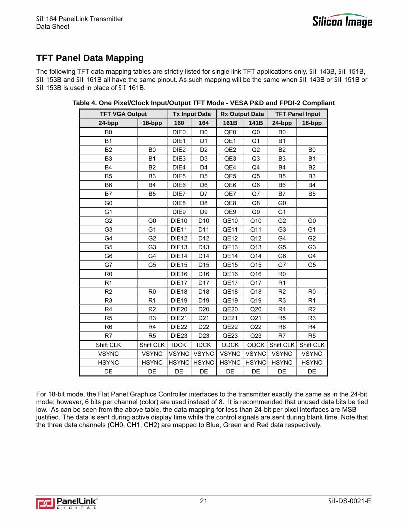
TFT Panel Data Mapping The following TFT data mapping tables are strictly listed for single link TFT applications only. SiI 143B, SiI 151B, SiI 153B and SiI 161B all have the same pinout. As such mapping will be the same when SiI 143B or SiI 151B or SiI 153B is used in place of SiI 161B.
Table 4. One Pixel/Clock Input/Output TFT Mode - VESA P&D and FPDI-2 Compliant TFT VGA Output Tx Input Data Rx Output Data TFT Panel Input 24-bpp 18-bpp 160 164 161B 141B 24-bpp 18-bpp
B0 DIE0 D0 QE0 Q0 B0 B1 DIE1 D1 QE1 Q1 B1 B2 B0 DIE2 D2 QE2 Q2 B2 B0 B3 B1 DIE3 D3 QE3 Q3 B3 B1 B4 B2 DIE4 D4 QE4 Q4 B4 B2 B5 B3 DIE5 D5 QE5 Q5 B5 B3 B6 B4 DIE6 D6 QE6 Q6 B6 B4 B7 B5 DIE7 D7 QE7 Q7 B7 B5 G0 DIE8 D8 QE8 Q8 G0 G1 DIE9 D9 QE9 Q9 G1 G2 G0 DIE10 D10 QE10 Q10 G2 G0 G3 G1 DIE11 D11 QE11 Q11 G3 G1 G4 G2 DIE12 D12 QE12 Q12 G4 G2 G5 G3 DIE13 D13 QE13 Q13 G5 G3 G6 G4 DIE14 D14 QE14 Q14 G6 G4 G7 G5 DIE15 D15 QE15 Q15 G7 G5 R0 DIE16 D16 QE16 Q16 R0 R1 DIE17 D17 QE17 Q17 R1 R2 R0 DIE18 D18 QE18 Q18 R2 R0 R3 R1 DIE19 D19 QE19 Q19 R3 R1 R4 R2 DIE20 D20 QE20 Q20 R4 R2 R5 R3 DIE21 D21 QE21 Q21 R5 R3 R6 R4 DIE22 D22 QE22 Q22 R6 R4 R7 R5 DIE23 D23 QE23 Q23 R7 R5
Shift CLK Shift CLK IDCK IDCK ODCK ODCK Shift CLK Shift CLK VSYNC VSYNC VSYNC VSYNC VSYNC VSYNC VSYNC VSYNC HSYNC HSYNC HSYNC HSYNC HSYNC HSYNC HSYNC HSYNC
DE DE DE DE DE DE DE DE For 18-bit mode, the Flat Panel Graphics Controller interfaces to the transmitter exactly the same as in the 24-bit mode; however, 6 bits per channel (color) are used instead of 8. It is recommended that unused data bits be tied low. As can be seen from the above table, the data mapping for less than 24-bit per pixel interfaces are MSB justified. The data is sent during active display time while the control signals are sent during blank time. Note that the three data channels (CH0, CH1, CH2) are mapped to Blue, Green and Red data respectively.

SiI 164 PanelLink Transmitter Data Sheet
SiI-DS-0021-E 22
Table 5. 24-bit One Pixel/Clock Input with 24-bit Two Pixels/Clock Output TFT Mode TFT VGA Output Tx Input Data Rx Output Data TFT Panel Input
24-bpp 160 164 161B 24-bpp B0 DIE0 D0 QE0 B0 - 0 B1 DIE1 D1 QE1 B1 - 0 B2 DIE2 D2 QE2 B2 - 0 B3 DIE3 D3 QE3 B3 - 0 B4 DIE4 D4 QE4 B4 - 0 B5 DIE5 D5 QE5 B5 - 0 B6 DIE6 D6 QE6 B6 - 0 B7 DIE7 D7 QE7 B7 - 0 G0 DIE8 D8 QE8 G0 - 0 G1 DIE9 D9 QE9 G1 - 0 G2 DIE10 D10 QE10 G2 - 0 G3 DIE11 D11 QE11 G3 - 0 G4 DIE12 D12 QE12 G4 - 0 G5 DIE13 D13 QE13 G5 - 0 G6 DIE14 D14 QE14 G6 - 0 G7 DIE15 D15 QE15 G7 - 0 R0 DIE16 D16 QE16 R0 - 0 R1 DIE17 D17 QE17 R1 - 0 R2 DIE18 D18 QE18 R2 - 0 R3 DIE19 D19 QE19 R3 - 0 R4 DIE20 D20 QE20 R4 - 0 R5 DIE21 D21 QE21 R5 - 0 R6 DIE22 D22 QE22 R6 - 0 R7 DIE23 D23 QE23 R7 - 0
QO0 B0 - 1 QO1 B1 - 1 QO2 B2 - 1 QO3 B3 - 1 QO4 B4 - 1 QO5 B5 - 1 QO6 B6 - 1 QO7 B7 - 1 QO8 G0 - 1 QO9 G1 - 1 QO10 G2 - 1 QO11 G3 - 1 QO12 G4 - 1 QO13 G5 - 1 QO14 G6 - 1 QO15 G7 - 1 QO16 R0 - 1 QO17 R1 - 1 QO18 R2 - 1 QO19 R3 - 1 QO20 R4 - 1 QO21 R5 - 1 QO22 R6 - 1 QO23 R7 - 1
Shift CLK IDCK IDCK ODCK Shift CLK/2 VSYNC VSYNC VSYNC VSYNC VSYNC HSYNC HSYNC HSYNC HSYNC HSYNC
DE DE DE DE DE
SiI 164 PanelLink Transmitter Data Sheet
23 SiI-DS-0021-E
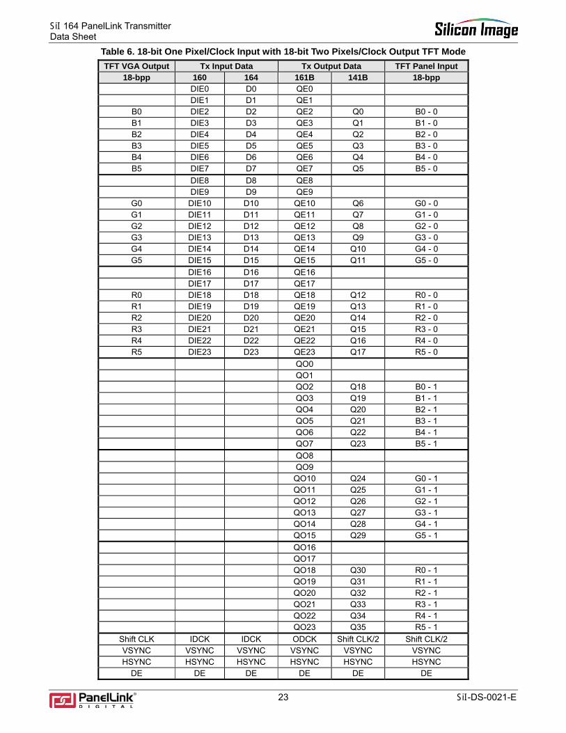
Table 6. 18-bit One Pixel/Clock Input with 18-bit Two Pixels/Clock Output TFT Mode TFT VGA Output Tx Input Data Tx Output Data TFT Panel Input
18-bpp 160 164 161B 141B 18-bpp DIE0 D0 QE0 DIE1 D1 QE1
B0 DIE2 D2 QE2 Q0 B0 - 0 B1 DIE3 D3 QE3 Q1 B1 - 0 B2 DIE4 D4 QE4 Q2 B2 - 0 B3 DIE5 D5 QE5 Q3 B3 - 0 B4 DIE6 D6 QE6 Q4 B4 - 0 B5 DIE7 D7 QE7 Q5 B5 - 0
DIE8 D8 QE8 DIE9 D9 QE9
G0 DIE10 D10 QE10 Q6 G0 - 0 G1 DIE11 D11 QE11 Q7 G1 - 0 G2 DIE12 D12 QE12 Q8 G2 - 0 G3 DIE13 D13 QE13 Q9 G3 - 0 G4 DIE14 D14 QE14 Q10 G4 - 0 G5 DIE15 D15 QE15 Q11 G5 - 0
DIE16 D16 QE16 DIE17 D17 QE17
R0 DIE18 D18 QE18 Q12 R0 - 0 R1 DIE19 D19 QE19 Q13 R1 - 0 R2 DIE20 D20 QE20 Q14 R2 - 0 R3 DIE21 D21 QE21 Q15 R3 - 0 R4 DIE22 D22 QE22 Q16 R4 - 0 R5 DIE23 D23 QE23 Q17 R5 - 0
QO0 QO1 QO2 Q18 B0 - 1 QO3 Q19 B1 - 1 QO4 Q20 B2 - 1 QO5 Q21 B3 - 1 QO6 Q22 B4 - 1 QO7 Q23 B5 - 1 QO8 QO9 QO10 Q24 G0 - 1 QO11 Q25 G1 - 1 QO12 Q26 G2 - 1 QO13 Q27 G3 - 1 QO14 Q28 G4 - 1 QO15 Q29 G5 - 1 QO16 QO17 QO18 Q30 R0 - 1 QO19 Q31 R1 - 1 QO20 Q32 R2 - 1 QO21 Q33 R3 - 1 QO22 Q34 R4 - 1 QO23 Q35 R5 - 1
Shift CLK IDCK IDCK ODCK Shift CLK/2 Shift CLK/2 VSYNC VSYNC VSYNC VSYNC VSYNC VSYNC HSYNC HSYNC HSYNC HSYNC HSYNC HSYNC
DE DE DE DE DE DE

SiI 164 PanelLink Transmitter Data Sheet
SiI-DS-0021-E 24
Design Recommendations
1.5V to 3.3V I2C Bus Level-Shifting To program the SiI 164 via I2C mode SDA and SCL swing level must be 3.3V. DVO sources have I2C swing of 1.5V. To ensure proper initialization of the SiI 164 a bi-directional voltage level-shifting circuit between the SiI 164 I2C bus and the VGA or driving source should be implemented. Two suggested components that can be used to achieve this is by using either a dual N-channel transistor like Fairchild Semiconductor’s NDC7002N or the Philips GTL2010 High Speed Bus Switch. Refer to Figure 16 for a schematic example using a dual N-channel transistor for translating an I2C 1.5V signal to 3.3V I2C signal and vice versa.
1.5V
1.5V
1K
1.5V I2C DATA FROM VGA
2.2K
2.9V 3.3V
1KG
S D
Q2
2N70023
1
2
1.5V I2C CLK FROM VGA
3.3V2.9V
3.3V I2C CLK TO SiI 164
2.2K
3.3V I2C DATA TO SiI 164
G
S D
Q4
2N70023
1
2
Figure 16. I2C Bus Voltage Level-Shifting using Fairchild NDC7002N Figure 17 illustrates a schematic example using the Philips GTL 2010 to achieve a 1.5V to 3.3V bi-directional level-shift.
1.5V I2C DATA FROM VGA
R1 1K
3.3V I2C DATA TO SiI 164
R4
2.2K
R5
2.2K
3.3V I2C CLK TO SiI 164
3.3V
R3
200K
1.5V
R2 1K
5V
1.5V I2C CLK FROM VGA
U1
GTL2010
1234
242322212019181716151413
56789
101112
GNDSREFS1S2
GREFDREF
D1D2D3D4D5D6D7D8D9
D10
S3S4S5S6S7S8S9S10
Figure 17. I2C Bus Voltage Level Shifting using Philips GTL 2010

SiI 164 PanelLink Transmitter Data Sheet
25 SiI-DS-0021-E
Voltage Ripple Regulation The power supply to PVCC is very important to the proper operation of the Transmitter chips. PVCC does not draw much current so any voltage regulator that can supply 50mA or more is sufficient. Two suggested voltage regulators are TL431 from Texas Instruments or LM317 from National Semiconductor. Two examples are shown in Figure 18 and Figure 19
Vin (5V) Vout (3.3V) to PVCC1and PVCC2
TL431
100-150 ohms
1K ohms1%
3K ohms1%
Vref
Cathode
Anode
Ref
Figure 18. Voltage Regulation using TL431
Decoupling and bypass capacitors are also involved with power supply connections, as described in detail in Figure 20 and Figure 21.
Vout (3.3V) to PVCC1and PVCC2Vin (5V)
240 ohms
390 ohms
VIN VOUT
ADJ
LM317EMP
Figure 19. Voltage Regulation using LM317

SiI 164 PanelLink Transmitter Data Sheet
SiI-DS-0021-E 26
Decoupling Capacitors Designers should include decoupling and bypass capacitors at each power pin in the layout. These are shown schematically in Figure 21. Place these components as closely as possible to the SiI 164 pins, and avoid routing through vias if possible, as shown in Figure 20, which is representative of the various types of power pins on the transmitter.
C1
VCC
Ferrite
Via to GND
VCC
GND
C2
C3
L1
Figure 20. Decoupling and Bypass Capacitor Placement
VCCPIN
C1 C2
L1
C3
VCC
Figure 21. Decoupling and Bypass Schematic
The values shown in Table 7 are recommendations that should be adjusted according to the noise characteristics of the specific board-level design. Pins in one group (such as VCC) may share C2, L1, and C3, each pin having C1 placed as closely to the pin as possible.
Table 7. Recommended Components for Bypass and Decoupling Circuits C1 C2 C3 L1
100 – 300 pF 2.2 – 10 µF 10 µF 200+ Ω
SiI 164 PanelLink Transmitter Data Sheet
27 SiI-DS-0021-E
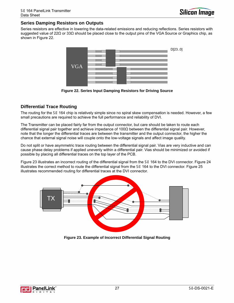
Series Damping Resistors on Outputs Series resistors are effective in lowering the data-related emissions and reducing reflections. Series resistors with suggested value of 22Ω or 33Ω should be placed close to the output pins of the VGA Source or Graphics chip, as shown in Figure 22.
D[23..0]
VGA
Figure 22. Series Input Damping Resistors for Driving Source
Differential Trace Routing The routing for the SiI 164 chip is relatively simple since no spiral skew compensation is needed. However, a few small precautions are required to achieve the full performance and reliability of DVI.
The Transmitter can be placed fairly far from the output connector, but care should be taken to route each differential signal pair together and achieve impedance of 100Ω between the differential signal pair. However, note that the longer the differential traces are between the transmitter and the output connector, the higher the chance that external signal noise will couple onto the low-voltage signals and affect image quality.
Do not split or have asymmetric trace routing between the differential signal pair. Vias are very inductive and can cause phase delay problems if applied unevenly within a differential pair. Vias should be minimized or avoided if possible by placing all differential traces on the top layer of the PCB.
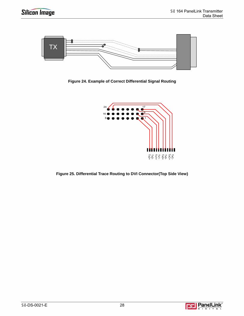
Figure 23 illustrates an incorrect routing of the differential signal from the SiI 164 to the DVI connector. Figure 24 illustrates the correct method to route the differential signal from the SiI 164 to the DVI connector. Figure 25 illustrates recommended routing for differential traces at the DVI connector.
TX
Figure 23. Example of Incorrect Differential Signal Routing
SiI 164 PanelLink Transmitter Data Sheet
SiI-DS-0021-E 28
TX
Figure 24. Example of Correct Differential Signal Routing
TxC-
TxC+
Tx0-Tx0+Tx1-Tx1+Tx2-Tx2+
18
916
1724
Figure 25. Differential Trace Routing to DVI Connector(Top Side View)
SiI 164 PanelLink Transmitter Data Sheet
29 SiI-DS-0021-E
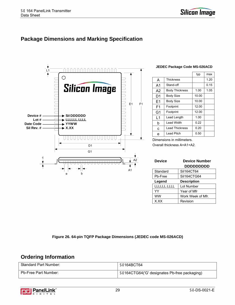
Package Dimensions and Marking Specification
SiIDDDDDDLLLLLL.LLLLYYWWX.XX
Device #Lot #
Date CodeSiI Rev. #
E1 F1
D1
G1
A2
A1e b
L1
c
JEDEC Package Code MS-026ACD
typ max
A Thickness 1.20
A1 Stand-off 0.15
A2 Body Thickness 1.00 1.05
D1 Body Size 10.00
E1 Body Size 10.00
F1 Footprint 12.00
G1 Footprint 12.00
L1 Lead Length 1.00
b Lead Width 0.22
c Lead Thickness 0.20
e Lead Pitch 0.50
Dimensions in millimeters. Overall thickness A=A1+A2.
Device Device Number DDDDDDDDD
Standard SiI164CT64 Pb-Free SiI164CTG64 Legend Description LLLLLL.LLLL Lot Number YY Year of Mfr WW Work Week of Mfr. X.XX Revision
Figure 26. 64-pin TQFP Package Dimensions (JEDEC code MS-026ACD)
Ordering Information Standard Part Number: SiI164BCT64
Pb-Free Part Number: SiI164CTG64('G' designates Pb-free packaging)
SiI 164 PanelLink Transmitter Data Sheet
SiI-DS-0021-E 30
© 2005 Silicon Image. Inc. 06/05 SiI-DS-0021-E
Silicon Image, Inc. Tel: (408) 616-4000 1060 E. Arques Avenue Fax: (408) 830-9530 Sunnyvale, CA 94085 E-mail: [email protected] USA Web: www.siliconimage.com