test report of mppt & led driver pmp 7647 - … report - pmp7647_revc december 12th, 2013 1 tii...
TRANSCRIPT

Test Report - PMP7647_RevC
December 12th, 2013 1 TII - Reference Designs
TEST REPORT OF MPPT & LED DRIVER
PMP 7647

Test Report - PMP7647_RevC
December 12th, 2013 2 TII - Reference Designs
CONTENTS
Contents
I. INTRODUCTION .................................................................................................................................................................... 3 II. DESCRIPTION ........................................................................................................................................................................ 3 III. BLOCK DIAGRAM ............................................................................................................................................................ 4 IV. SPECIFICATIONS .............................................................................................................................................................. 5 V. BOARD LAYOUT .................................................................................................................................................................. 5 VI. TEST SETUP ....................................................................................................................................................................... 6 VII. TEST DATA ........................................................................................................................................................................ 7 a. MPPT PERFORMANCE ......................................................................................................................................................... 7 b. LED DRIVER PERFORMANCE ............................................................................................................................................ 7 c. MPPT EFFICIENCY PLOT .................................................................................................................................................... 7 VIII. WAVEFORMS .................................................................................................................................................................... 8
a. Switching Node Waveforms ................................................................................................................................................ 8 b. Gate waveforms ................................................................................................................................................................... 9
IX. POWER GAIN WITH MPP .............................................................................................................................................. 10 a. Test Set-up ......................................................................................................................................................................... 10 b. Test Results ........................................................................................................................................................................ 10
X. SCHEMATIC ......................................................................................................................................................................... 11 a. Power Stage ....................................................................................................................................................................... 11 b. Controller and Bias Supply ................................................................................................................................................ 12
XI. BILL OF MATERIALS ..................................................................................................................................................... 13 XII. CONCLUSION .................................................................................................................................................................. 13 XIII. APPENDIX ........................................................................................................................................................................ 14

Test Report - PMP7647_RevC
December 12th, 2013 3 TII - Reference Designs
I. INTRODUCTION
The following document is a compilation of test results of the PMP7647 reference design, a 12A MPPT solar charge controller & 700mA LED driver. The test results are taken with simulated solar panel input corresponding to 12V panel.
II. DESCRIPTION
The PMP7647 is developed around the MSP430F5132 controller IC. The design is targeted for low power solar charger and LED driver solutions such as solar street lights. This design is capable of charging 12V batteries with up to 10A output current from 12V panels. However, it can be easily adapted to 24V systems by just changing the MOSFETs to 60V rated parts. Also, the design can drive up to 15 LEDs in series with 700mA of current. It is possible to adapt the design for LED currents up to 1.1A with minimum change in hardware.
The MPPT section has a typical electrical efficiency of 97% at full load. This efficiency figure includes the losses in battery reverse protection and panel reverse flow protection MOSFETs, which are part of the design. The high efficiency is the result of the low gate charge MOSFETs from TI used in the design, and also the optimum layout. Another feature is the relatively small sized components used, possible due to the high operating frequency (settable from 100 - 200 KHz). The design has built-in battery charge profile for 12V Lead acid batteries. The design presently uses ‘perturb and observe’ algorithm for MPP tracking. This gives fast acquisition of MPP operation.
The LED driver section is a boost converter. The electrical efficiency of boost section is about 93% while driving 12 LEDs at 700mA, and is around 91% while driving 6 LEDs at 350mA. The section is protected with load and converter cut-off during overload, short circuit and load open fault situations. There is also provision to dim the output after specified time intervals. Though in a typical application the time intervals are in hours, the board is programmed for one minute intervals of 700mA and 350mA current drive for easy demonstration of the feature. The design is also capable of detection of ambient light based on the panel voltage, and taking appropriate decisions to turn on LEDs, charge battery in MPPT mode or go to standby accordingly. Low battery voltage protection by dimming the LEDs to 10% brightness and subsequently going to low power mode with further reduction in voltage is also implemented. The voltage levels at which these actions are taken can be set by software.
The various parameters of the circuit like battery charge current, load current, load timing pattern, battery under voltage set points etc can be set using a GUI made for the design. This makes customization a lot easier.
The circuit takes only under 4mA of standby current while operating from battery. This is further reduced to under 1mA while the circuit is in battery under voltage cut-off. Software programmable indications are provided in hardware, but are left non-configured.
Surge protection and EMI filtering components are not present on this design, and has to be added depending upon required specification levels.

Test Report - PMP7647_RevC
December 12th, 2013 4 TII - Reference Designs
III. BLOCK DIAGRAM

Test Report - PMP7647_RevC
December 12th, 2013 5 TII - Reference Designs
IV. SPECIFICATIONS
Input Voltage Range: 15VDC - 22VDC Storage: 12V battery Charging Current: 10A, with current limit set at 12A Output: 12 LEDs at 700mA Board Form Factor: 100 mm x 45 mm x 32 mm Expected efficiency: >95% for MPPT charger, and >90% for LED driver V. BOARD LAYOUT

Test Report - PMP7647_RevC
December 12th, 2013 6 TII - Reference Designs
VI. TEST SETUP
Input conditions: Panel input: 15VDC to 22VDC Set current limit to the short circuit current of panel when DC source is used instead of panel Storage: 12V battery Output: 12 LED array Equipment Used:
1. Current limited DC source simulating solar panel 2. Digital Oscilloscope 3. Multimeters 4. LED load/LED simulator
Procedure:
1. Connect appropriate battery to the battery terminals of the PMP7647 reference board, maintaining correct polarity.
2. Connect panel or current limited DC source to panel terminals, maintaining correct polarity.
3. Set the output voltage of DC source to slightly above the MPP voltage of the panel being simulated (if DC source is used instead of panel) and turn on.
4. Observe for gradual build-up of battery charge current. 5. Connect LED array to the load terminals with proper polarity. 6. Turn off the panel input to observe gradual build-up of LED current.
Connection Diagram:
A
V
A
V SOLAR PANEL BATTERY
A
V
+ + + - - -
LED ARRAY

Test Report - PMP7647_RevC
December 12th, 2013 7 TII - Reference Designs
VII. TEST DATA
a. MPPT PERFORMANCE
Vi (V) Ii (A) Vo (V) Io (A) Pi (W) Po (W) Efficiency
17.04 0.44 13.04 0.50 7.43 6.56 88.29 17.38 0.81 13.11 1.01 14.13 13.18 93.25
17.18 2.01 13.33 2.50 34.53 33.33 96.51
16.87 4.17 13.68 5.00 70.28 68.41 97.34
17.01 6.35 14.03 7.50 108.00 105.23 97.43
16.62 8.93 14.39 10.02 148.42 144.19 97.15
b. LED DRIVER PERFORMANCE
Vi (V) Ii (A) Vo (V) Io (A) Pi (W) Po (W) Efficiency
11.23 2.775 41.23 0.702 31.16 28.94 92.88
12.15 0.708 21.55 0.365 8.60 7.87 91.44
c. MPPT EFFICIENCY PLOT

Test Report - PMP7647_RevC
December 12th, 2013 8 TII - Reference Designs
VIII. WAVEFORMS
a. Switching Node Waveforms
MPPT switch node at 10A charging current
Boost converter switch node at 12LED, 700mA load

Test Report - PMP7647_RevC
December 12th, 2013 9 TII - Reference Designs
b. Gate waveforms
MPPT gate waveforms at 10A load show dead-time implementation
Expanded view

Test Report - PMP7647_RevC
December 12th, 2013 10 TII - Reference Designs
IX. POWER GAIN WITH MPP
a. Test Set-up
This test was done with an earlier similar design PMP7605. Setup Explains the Power flow from Panel to Battery during MPPT Operation. To connect Panel directly to battery, both contactors were opened and Extra connections were connected directly onto the battery.
b. Test Results
12 V SystemBattery Voltage = 11.96Two Panels connected Readings Taken approximately every 5-7 mins (@ 3.15 pm) Cloudy Conditions
Sr No ImprovementPanel directly connected to Battery Charging via MPPT Board %
1 1.794 2.08 15.942 1.28 1.443 12.733 0.55 0.6 9.094 1.15 1.3 13.045 1.21 1.35 11.576 2.13 2.5 17.37
Charging Currents (A)
Test Report - PMP7647_RevC
December 12th, 2013 11 TII - Reference Designs
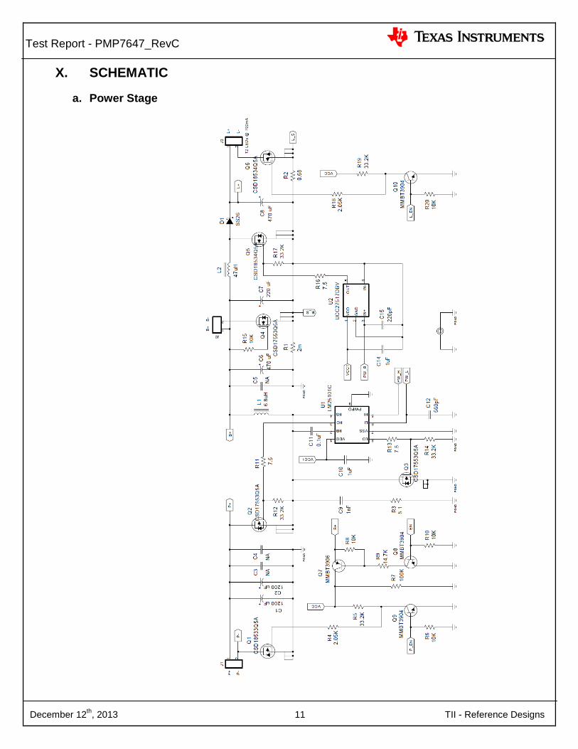
X. SCHEMATIC
a. Power Stage
Test Report - PMP7647_RevC
December 12th, 2013 12 TII - Reference Designs
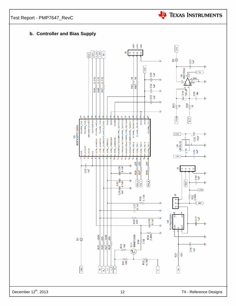
b. Controller and Bias Supply

Test Report - PMP7647_RevC
December 12th, 2013 13 TII - Reference Designs
XI. BILL OF MATERIALS
XII. CONCLUSION
The board is tested for the given specifications and found to meet them. Further optimization of software can be done depending on specific system requirements.
Item Qty Reference Value Description Part Number Manufacturer Size1 2 B2, B3 Bead, Ferrite, 500mA, 600ohms 7427920415 Wurth Elektronik 8052 2 C1, C2 1200 uF Capacitor, Aluminium Electrolytic, Low ESR, 35V EEU-FM1V122L Panasonic 12.5 x 30 mm3 1 C6 470 uF Capacitor, Aluminium Electrolytic, Low ESR, 35V EEU-FR1V471L Panasonic 8 x 22 mm2 1 C7 220 uF Capacitor, Aluminium Electrolytic, Low ESR, 35V UHE1V221MPD6 Nichicon 10 x 12.5 mm3 1 C8 470 uF Capacitor, Aluminium Electrolytic, Low ESR, 63V UPW1J471MHD Nichicon 12.5 x 25 mm4 3 C9, C18, C28 1nF Capacitor, Ceramic, 50V, X7R, 10% Std Std 603
5 10
C10, C14, C16, C17, C21, C22, C23, C24, C25, C31 1uF Capacitor, Ceramic, 25V, X7R, 10% TMK107B7105KA-T Taiyo-Yuden 603
6 5C11, C26, C27, C29, C30 0.1uF Capacitor, Ceramic, 50V, X7R, 10% Std Std 603
7 1 C12 560pF Capacitor, Ceramic, 50V, NPO, 1% Std Std 6038 1 C15 220pF Capacitor, Ceramic, 50V, NPO, 1% Std Std 6039 1 C19 100 uF Capacitor, Aluminium, 10V, 20% EEU-EB1A101 Panasonic 5 x 11 mm
10 1 C32 10uF Capacitor, Aluminium, 10V, 20% 50YXM10MEFC5X11 Rubycon 5 x 11 mm11 1 D1 SS26 Diode, Schottky, 2A, 60V SS26-TP MCC Semi SMA12 3 J1, J2, J3 OSTTC022162 Terminal Block, 2-pin, 15-A, 5.1mm OSTTC022162 OST 0.40 x 0.35 inch13 1 J4 PEC36SAAN Header, Male 3-pin, 100mil spacing, (36-pin strip) PEC36SAAN Sullins 0.100 inch x 314 2 J5, J6 PEC36SAAN Header, Male 4-pin, 100mil spacing, (36-pin strip) PEC36SAAN Sullins 0.100 inch x 415 1 L1 6.8uH Inductor, SMT, 18.5-A, 4.1-milliohm 7443556680 Wurth Elektronik 18 x 18 x 9 mm16 1 L2 47uH Inductor, SMT, 3.6-A, 60-milliohm 7447709470 Wurth Elektronik 12 x 12 x 10 mm17 1 Q1 CSD18533Q5A MOSFET, N-Chan, 60V, 103A, 5.9 mOhm CSD18533Q5A TI QFN-8 POWER18 2 Q5, Q6 CSD18534Q5A MOSFET, N-Chan, 60V, 50A, 9.8 mOhm CSD18534Q5A TI QFN-8 POWER19 3 Q2, Q3, Q4 CSD17553Q5A MOSFET, N-Chan, 30V, 23.5A, 2.7 mOhm CSD17553Q5A TI QFN-8 POWER20 2 Q7, Q11 MMBT3906 Trans, PNP, 40-V, 200-mA, 225-mW MMBT3906LT1G On Semi SOT2321 3 Q8, Q9, Q10 MMBT3904 Trans, NPN, 40-V, 200-mA,225-mW MMBT3904LT1G On Semi SOT2322 1 R1 2m Resistor, 2 milliOhm, 3W, 1% LRMAP2512-R002FT4 TT/Welwyn 251223 1 R2 0.68 Resistor, 0.68 Ohm, 2W, 1% CSRN2512FKR680 Stackpole 251224 1 R3 5.1 Resistor, 5.1Ohm, 1W, 5% Std Std 251225 3 R4, R18, R22 2.05K Resistor, Chip, 1/16W, 1% Std Std 603
26 5R5, R12, R14, R17, R19 33.2K Resistor, Chip, 1/16W, 1% Std Std 603
27 7R6, R8, R10, R15, R20, R31, R33 10K Resistor, Chip, 1/16W, 1% Std Std 603
28 1 R7 100K Resistor, Chip, 1/16W, 1% Std Std 60329 3 R11, R13, R16 7.5 Resistor, Chip, 1/10W, 5% Std Std 80530 1 R21 681 Resistor, Chip, 1/4 watt, ± 5% Std Std 120631 2 R23, R24 10 Resistor, Chip, 1/16W, 1% Std Std 60332 1 R25 100K Resistor, Chip, 1/10W, 1% Std Std 805
33 5R26, R28, R36, R37, R38 205 Resistor, Chip, 1/16W, 1% Std Std 603
34 1 R27 154K Resistor, Chip, 1/10W, 1% Std Std 80535 1 R29 14K Resistor, Chip, 1/16W, 1% Std Std 60336 2 R9, R32 14.7K Resistor, Chip, 1/16W, 1% Std Std 60337 1 R34 7.5K Resistor, Chip, 1/16W, 1% Std Std 60338 1 R35 2.49K Resistor, Chip, 1/16W, 1% Std Std 60339 4 R30, R39, R40, R41 5.11K Resistor, Chip, 1/16W, 1% Std Std 60340 2 R42, R43 1K Resistor, Chip, 1/16W, 1% Std Std 60341 1 U1 LM25101C 1A 80V Half-Bridge Gate Driver LM25101CMAX TI SO842 1 U2 UCC27517DBV IC, 4A Single Channel High-Speed Low-Side Gate Drivers UCC27517DBV TI SOT23-543 1 U3 MSP430F5132IDA IC, Mixed Signal Microcontroller MSP430F5132IDA TI MSOP-3844 1 U4 TLV70433DBV IC, 24-V Input, 150 mA, Utralow IQ LDO Regulator TLV70433DBV TI SOT-2345 1 U5 INA199A2 IC, Current shunt monitor, Bi-Directional Zerø-Drift Series INA199A2DCK TI SC-7046 1 U6 uA78L10A IC, 3 Pin 100mA Fixed 10V Positive Voltage Regulator UA78L10ACLPR TI TO-92
PMP7647 BOM Revision C

Test Report - PMP7647_RevC
December 12th, 2013 14 TII - Reference Designs
XIII. APPENDIX
For Feasibility Evaluation Only, in Laboratory/Development Environments. The EVM is not a complete product. It is intended solely for use for preliminary feasibility evaluation in laboratory / development environments by technically qualified electronics experts who are familiar with the dangers and application risks associated with handling electrical / mechanical components, systems and subsystems. It should not be used as all or part of a production unit.
Your Sole Responsibility and Risk. You acknowledge, represent and agree that: 1. You have unique knowledge concerning Federal, State and local regulatory requirements (including but not
limited to Food and Drug Administration regulations, if applicable) which relate to your products and which relate to your use (and/or that of your employees, affiliates, contractors or designees) of the EVM for evaluation, testing and other purposes.
2. You have full and exclusive responsibility to assure the safety and compliance of your products with all such laws and other applicable regulatory requirements, and also to assure the safety of any activities to be conducted by you and/or your employees, affiliates, contractors or designees, using the EVM. Further, you are responsible to assure that any interfaces (electronic and/or mechanical) between the EVM and any human body are designed with suitable isolation and means to safely limit accessible leakage currents to minimize the risk of electrical shock hazard.
3. Since the EVM is not a completed product, it may not meet all applicable regulatory and safety compliance standards (such as UL, CSA, VDE, CE, RoHS and WEEE) which may normally be associated with similar items. You assume full responsibility to determine and/or assure compliance with any such standards and related certifications as may be applicable. You will employ reasonable safeguards to ensure that your use of the EVM will not result in any property damage, injury or death, even if the EVM should fail to perform as described or expected.
Certain Instructions. Exceeding the specified EVM ratings (including but not limited to input and output voltage, current, power, and environmental ranges) may cause property damage, personal injury or death. If there are questions concerning these ratings please contact a TI field representative prior to connecting interface electronics including input power and intended loads. Any loads applied outside of the specified output range may result in unintended and/or inaccurate operation and/or possible permanent damage to the EVM and/or interface electronics. Please consult the EVM User’s Guide prior to connecting any load to the EVM output. If there is uncertainty as to the load specification, please contact a TI field representative. During normal operation, some circuit components may have case temperatures greater than 60°C as long as the input and output ranges are maintained at nominal ambient operating temperature. These components include but are not limited to linear regulators, switching transistors, pass transistors, and current sense resistors which can be indentified using the EVM schematic located in the EVM User’s Guide. When placing measurement probes near these devices during normal operation, please be aware that these devices may be very warm to the touch.
Agreement to Defend, Indemnify and Hold Harmless. You agree to defend, indemnify and hold TI, its licensors and their representatives harmless from and against any and all claims, damages, losses, expenses, costs and liabilities (collectively, “Claims”) arising out of or in connection with any use of the EVM that is not in accordance with the terms of this agreement. This obligation shall apply whether Claims arise under the law of tort or contract or any other legal theory, and even if the EVM fails to perform as described or expected.
Safety-Critical or Life-Critical Applications. If you intend to evaluate TI components for possible use in safety-critical applications (such as life support) where a failure of the TI product would reasonably be expected to cause severe personal injury or death, such as devices which are classified as FDA Class III or similar classification, then you must specifically notify TI of such intent and enter into a separate Assurance and Indemnity Agreement.
EVALUATION BOARD/KIT/MODULE (EVM) WARNINGS, RESTRICTIONS AND DISCLAIMER

IMPORTANT NOTICE FOR TI REFERENCE DESIGNSTexas Instruments Incorporated ("TI") reference designs are solely intended to assist designers (“Buyers”) who are developing systems thatincorporate TI semiconductor products (also referred to herein as “components”). Buyer understands and agrees that Buyer remainsresponsible for using its independent analysis, evaluation and judgment in designing Buyer’s systems and products.TI reference designs have been created using standard laboratory conditions and engineering practices. TI has not conducted anytesting other than that specifically described in the published documentation for a particular reference design. TI may makecorrections, enhancements, improvements and other changes to its reference designs.Buyers are authorized to use TI reference designs with the TI component(s) identified in each particular reference design and to modify thereference design in the development of their end products. HOWEVER, NO OTHER LICENSE, EXPRESS OR IMPLIED, BY ESTOPPELOR OTHERWISE TO ANY OTHER TI INTELLECTUAL PROPERTY RIGHT, AND NO LICENSE TO ANY THIRD PARTY TECHNOLOGYOR INTELLECTUAL PROPERTY RIGHT, IS GRANTED HEREIN, including but not limited to any patent right, copyright, mask work right,or other intellectual property right relating to any combination, machine, or process in which TI components or services are used.Information published by TI regarding third-party products or services does not constitute a license to use such products or services, or awarranty or endorsement thereof. Use of such information may require a license from a third party under the patents or other intellectualproperty of the third party, or a license from TI under the patents or other intellectual property of TI.TI REFERENCE DESIGNS ARE PROVIDED "AS IS". TI MAKES NO WARRANTIES OR REPRESENTATIONS WITH REGARD TO THEREFERENCE DESIGNS OR USE OF THE REFERENCE DESIGNS, EXPRESS, IMPLIED OR STATUTORY, INCLUDING ACCURACY ORCOMPLETENESS. TI DISCLAIMS ANY WARRANTY OF TITLE AND ANY IMPLIED WARRANTIES OF MERCHANTABILITY, FITNESSFOR A PARTICULAR PURPOSE, QUIET ENJOYMENT, QUIET POSSESSION, AND NON-INFRINGEMENT OF ANY THIRD PARTYINTELLECTUAL PROPERTY RIGHTS WITH REGARD TO TI REFERENCE DESIGNS OR USE THEREOF. TI SHALL NOT BE LIABLEFOR AND SHALL NOT DEFEND OR INDEMNIFY BUYERS AGAINST ANY THIRD PARTY INFRINGEMENT CLAIM THAT RELATES TOOR IS BASED ON A COMBINATION OF COMPONENTS PROVIDED IN A TI REFERENCE DESIGN. IN NO EVENT SHALL TI BELIABLE FOR ANY ACTUAL, SPECIAL, INCIDENTAL, CONSEQUENTIAL OR INDIRECT DAMAGES, HOWEVER CAUSED, ON ANYTHEORY OF LIABILITY AND WHETHER OR NOT TI HAS BEEN ADVISED OF THE POSSIBILITY OF SUCH DAMAGES, ARISING INANY WAY OUT OF TI REFERENCE DESIGNS OR BUYER’S USE OF TI REFERENCE DESIGNS.TI reserves the right to make corrections, enhancements, improvements and other changes to its semiconductor products and services perJESD46, latest issue, and to discontinue any product or service per JESD48, latest issue. Buyers should obtain the latest relevantinformation before placing orders and should verify that such information is current and complete. All semiconductor products are soldsubject to TI’s terms and conditions of sale supplied at the time of order acknowledgment.TI warrants performance of its components to the specifications applicable at the time of sale, in accordance with the warranty in TI’s termsand conditions of sale of semiconductor products. Testing and other quality control techniques for TI components are used to the extent TIdeems necessary to support this warranty. Except where mandated by applicable law, testing of all parameters of each component is notnecessarily performed.TI assumes no liability for applications assistance or the design of Buyers’ products. Buyers are responsible for their products andapplications using TI components. To minimize the risks associated with Buyers’ products and applications, Buyers should provideadequate design and operating safeguards.Reproduction of significant portions of TI information in TI data books, data sheets or reference designs is permissible only if reproduction iswithout alteration and is accompanied by all associated warranties, conditions, limitations, and notices. TI is not responsible or liable forsuch altered documentation. Information of third parties may be subject to additional restrictions.Buyer acknowledges and agrees that it is solely responsible for compliance with all legal, regulatory and safety-related requirementsconcerning its products, and any use of TI components in its applications, notwithstanding any applications-related information or supportthat may be provided by TI. Buyer represents and agrees that it has all the necessary expertise to create and implement safeguards thatanticipate dangerous failures, monitor failures and their consequences, lessen the likelihood of dangerous failures and take appropriateremedial actions. Buyer will fully indemnify TI and its representatives against any damages arising out of the use of any TI components inBuyer’s safety-critical applications.In some cases, TI components may be promoted specifically to facilitate safety-related applications. With such components, TI’s goal is tohelp enable customers to design and create their own end-product solutions that meet applicable functional safety standards andrequirements. Nonetheless, such components are subject to these terms.No TI components are authorized for use in FDA Class III (or similar life-critical medical equipment) unless authorized officers of the partieshave executed an agreement specifically governing such use.Only those TI components that TI has specifically designated as military grade or “enhanced plastic” are designed and intended for use inmilitary/aerospace applications or environments. Buyer acknowledges and agrees that any military or aerospace use of TI components thathave not been so designated is solely at Buyer's risk, and Buyer is solely responsible for compliance with all legal and regulatoryrequirements in connection with such use.TI has specifically designated certain components as meeting ISO/TS16949 requirements, mainly for automotive use. In any case of use ofnon-designated products, TI will not be responsible for any failure to meet ISO/TS16949.
Mailing Address: Texas Instruments, Post Office Box 655303, Dallas, Texas 75265Copyright © 2014, Texas Instruments Incorporated