testing of digital systems: an introduction dr. aiman h. el-maleh computer engineering department...
TRANSCRIPT

Testing of Digital Systems:Testing of Digital Systems:An IntroductionAn Introduction
Testing of Digital Systems:Testing of Digital Systems:An IntroductionAn Introduction
Dr. Aiman H. El-Maleh
Computer Engineering Department
King Fahd University of Petroleum & Minerals
Dr. Aiman H. El-Maleh
Computer Engineering Department
King Fahd University of Petroleum & Minerals

1-2
OutlineOutlineOutlineOutline
Introduction Manufacturing Cost Defects, Faults, Fault Models Automatic Test Pattern Generation Scan Testing Methodology Built-In Self Test Conclusions
Most figures used in this presentation are taken from Design-for-Test for Digital IC’s and Embedded Core Systems by Alfred L. Crouch.
Introduction Manufacturing Cost Defects, Faults, Fault Models Automatic Test Pattern Generation Scan Testing Methodology Built-In Self Test Conclusions
Most figures used in this presentation are taken from Design-for-Test for Digital IC’s and Embedded Core Systems by Alfred L. Crouch.

1-3
VLSI Realization ProcessVLSI Realization ProcessVLSI Realization ProcessVLSI Realization Process
Determine requirements
Write specifications
Design synthesis and Verification
FabricationManufacturing test
Chips to customer
Customer’s need
Test development

1-4
DefinitionsDefinitionsDefinitionsDefinitions
Design synthesis: Given an I/O function, develop a procedure to manufacture a device using known materials and processes.
Verification: Predictive analysis to ensure that the synthesized design, when manufactured, will perform the given I/O function.
Test: A manufacturing step that ensures that the physical device, manufactured from the synthesized design, has no manufacturing defect.

1-5
Verification vs. TestVerification vs. TestVerification vs. TestVerification vs. Test
Verifies correctness of design.
Performed by simulation, hardware emulation, or formal methods.
Performed once prior to manufacturing.
Responsible for quality of design.
Verifies correctness of manufactured hardware.
Two-part process:• 1. Test generation: software
process executed once during design
• 2. Test application: electrical tests applied to hardware
Test application performed on every manufactured device.
Responsible for quality of devices.
Verification Test

1-6
Definition of TestingDefinition of TestingDefinition of TestingDefinition of Testing
A known input stimulus is applied to a unit in a known state, and a known response can be evaluated.
A known input stimulus is applied to a unit in a known state, and a known response can be evaluated.

1-7
ExampleExampleExampleExample
1-8
Reasons for TestingReasons for TestingReasons for TestingReasons for Testing
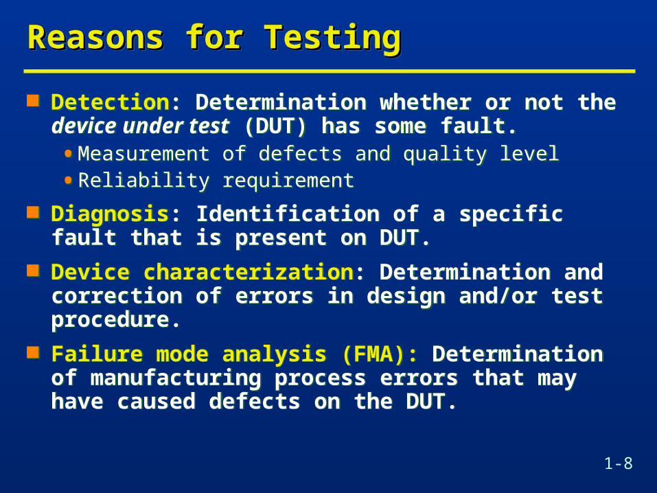
Detection: Determination whether or not the device under test (DUT) has some fault.• Measurement of defects and quality level
• Reliability requirement
Diagnosis: Identification of a specific fault that is present on DUT.
Device characterization: Determination and correction of errors in design and/or test procedure.
Failure mode analysis (FMA): Determination of manufacturing process errors that may have caused defects on the DUT.

1-9
Product Manufacturing CostProduct Manufacturing CostProduct Manufacturing CostProduct Manufacturing Cost

1-10
Product Manufacturing CostProduct Manufacturing CostProduct Manufacturing CostProduct Manufacturing Cost
Reduction of silicon cost • increasing volume and yield
• die size reduction (process shrinks or more efficient layout)
Reduction of packaging cost • increasing volume,
• shifting to lower cost packages if possible (e.g., from ceramic to plastic),
• reduction in package pin count
Reduction in cost of test • reducing vector data size
• reducing the cost of the tester
• reducing test time

1-11
Main Difficulties in TestingMain Difficulties in TestingMain Difficulties in TestingMain Difficulties in Testing
Miniaturization Physical access difficult or impossible.
Increasing complexity Large amount of test data.
Number of access ports remains constant Long test application time.
High speed High demand on tester’s driver/sensor mechanism and more complicated failure mechanism.
Testing accounts up to 50% of product development efforts.
The key to successful testing lies in the design process.

1-12
Main Difficulties in TestingMain Difficulties in TestingMain Difficulties in TestingMain Difficulties in Testing

1-13
Costs of TestingCosts of TestingCosts of TestingCosts of Testing
Design for testability (DFT)• Chip area overhead and yield reduction
• Performance overhead
Software processes of test• Test generation and fault simulation
• Test programming and debugging
Manufacturing test• Automatic test equipment (ATE) capital cost
• Test center operational cost
Design for testability (DFT)• Chip area overhead and yield reduction
• Performance overhead
Software processes of test• Test generation and fault simulation
• Test programming and debugging
Manufacturing test• Automatic test equipment (ATE) capital cost
• Test center operational cost

1-14
Cost of Manufacturing TestCost of Manufacturing TestCost of Manufacturing TestCost of Manufacturing Test
0.5-1.0GHz, analog instruments,1,024 digital pins:• ATE purchase price= $1.2M + 1,024 x $3,000 = $4.272M
Running cost (five-year linear depreciation)• = Depreciation + Maintenance + Operation
• = $0.854M + $0.085M + $0.5M
• = $1.439M/year
Test cost (24 hour ATE operation)• = $1.439M/(365 x 24 x 3,600)
• = 4.5 cents/second

1-15
Automatic Test Equipment ComponentsAutomatic Test Equipment ComponentsAutomatic Test Equipment ComponentsAutomatic Test Equipment Components
Powerful computer Powerful 32-bit Digital Signal Processor (DSP) for
analog testing Test Program (written in high-level language) running
on the computer Probe Head (actually touches the bare or packaged
chip to perform fault detection experiments) Probe Card or Membrane Probe (contains electronics
to measure signals on chip pin or pad)

1-16
ADVANTEST Model T6682 ATEADVANTEST Model T6682 ATEADVANTEST Model T6682 ATEADVANTEST Model T6682 ATE

1-17
LTX FUSION HF ATELTX FUSION HF ATELTX FUSION HF ATELTX FUSION HF ATE

1-18
Manufacturing Test BoardManufacturing Test BoardManufacturing Test BoardManufacturing Test Board
The chip will be accessed by the tester at its pins only
A custom (load) board will be made for this purpose
Each pin has a limited number of bits available (e.g., 2 MB)
Test program (set of vectors and tester control) applied at tester speed (may be less than actual chip speed)
Primary goal of manufacturing test is structural verification

1-19
Design For TestabilityDesign For TestabilityDesign For TestabilityDesign For Testability
To take into account the testing aspects during the design process so that more testable designs will be generated.
Advantages of DFT• Reduce test efforts.
• Eases generation of test vectors• Eases diagnosis & debugging
• Reduce cost for test equipments (ATE).
• Shorten turnaround time.
• Increase product quality.
Disadvantages of DFT• Adds complexity to design methodology
• Impacts design area, power, speed and package pins

1-20
DefectsDefectsDefectsDefects
Defects: physical problems that occur in silicon Common Silicon CMOS defects:
• Gate-oxide shorts
• Insufficient doping
• Process or mask errors
• Metal trace opens
• Metal trace bridges
• Open and plugged vias
• Short to power (Vdd) or Ground (Vss)
Defects: physical problems that occur in silicon Common Silicon CMOS defects:
• Gate-oxide shorts
• Insufficient doping
• Process or mask errors
• Metal trace opens
• Metal trace bridges
• Open and plugged vias
• Short to power (Vdd) or Ground (Vss)

1-21
DefectsDefectsDefectsDefects
1-22
FaultsFaultsFaultsFaults
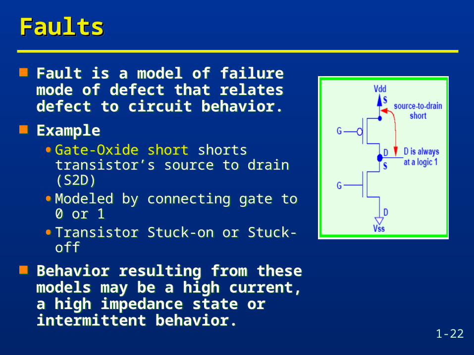
Fault is a model of failure mode of defect that relates defect to circuit behavior.
Example• Gate-Oxide short shorts transistor’s
source to drain (S2D)
• Modeled by connecting gate to 0 or 1
• Transistor Stuck-on or Stuck-off
Behavior resulting from these models may be a high current, a high impedance state or intermittent behavior.

1-23
Common Fault ModelsCommon Fault ModelsCommon Fault ModelsCommon Fault Models
Single stuck-at faults Transistor open and short faults Bridging faults Delay faults (transition, path) Memory faults PLA faults (stuck-at, cross-point, bridging) Functional faults (processors) Analog faults
Single stuck-at faults Transistor open and short faults Bridging faults Delay faults (transition, path) Memory faults PLA faults (stuck-at, cross-point, bridging) Functional faults (processors) Analog faults

1-24
Single Stuck-at Fault ModelSingle Stuck-at Fault ModelSingle Stuck-at Fault ModelSingle Stuck-at Fault Model
Failures represented as an individual wire shorted to Vdd (stuck-at-1) or Vss (stuck-at-0).
Covers many of physical defects.
Number of faults small. Independent of
technology. Can be used to model
other type of faults.
Failures represented as an individual wire shorted to Vdd (stuck-at-1) or Vss (stuck-at-0).
Covers many of physical defects.
Number of faults small. Independent of
technology. Can be used to model
other type of faults.

1-25
ExampleExampleExampleExample

1-26
Multiple Stuck-at FaultsMultiple Stuck-at FaultsMultiple Stuck-at FaultsMultiple Stuck-at Faults
A multiple stuck-at fault means that any set of lines is stuck-at some combination of (0,1) values.
The total number of multiple stuck-at faults in a circuit with k single fault sites is 3k-1.
A single fault test can fail to detect the target fault if another fault is also present, however, such masking of one fault by another is rare.
Statistically, single fault tests cover a very large number of multiple faults.

1-27
Transistor (Switch) FaultsTransistor (Switch) FaultsTransistor (Switch) FaultsTransistor (Switch) Faults
MOS transistor is considered an ideal switch and two types of faults are modeled:• Stuck-open -- a single transistor is permanently stuck in the
open state.
• Stuck-short -- a single transistor is permanently shorted irrespective of its gate voltage.
Detection of a stuck-open fault requires two vectors. Detection of a stuck-short fault requires the
measurement of quiescent current (IDDQ).

1-28
Stuck-Open ExampleStuck-Open ExampleStuck-Open ExampleStuck-Open Example
Two-vector s-op testcan be constructed byordering two s-at testsA
B
VDD
C
pMOSFETs
nMOSFETs
Stuck-open
1
0
0
0
0 1(Z)
Good circuit states
Faulty circuit states
Vector 1: test for A s-a-0(Initialization vector)
Vector 2 (test for A s-a-1)

1-29
Stuck-Short ExampleStuck-Short ExampleStuck-Short ExampleStuck-Short Example
A
B
VDD
C
pMOSFETs
nMOSFETs
Stuck-short
1
0
0 (X)
Good circuit state
Faulty circuit state
Test vector for A s-a-0
IDDQ path infaulty circuit

1-30
Delay FaultsDelay FaultsDelay FaultsDelay Faults
Some defects do not manifest a logical incorrect behavior but appear as an increase in delay
Example• Small metal open on a connection trace
• Logic value still propagates
• Propagation of value is slowed down
Some defects do not manifest a logical incorrect behavior but appear as an increase in delay
Example• Small metal open on a connection trace
• Logic value still propagates
• Propagation of value is slowed down

1-31
ExampleExampleExampleExample

1-32
Fault CoverageFault CoverageFault CoverageFault Coverage
Used as measure of test quality Used as measure of test quality
FaultsofNumber
FaultsDetectedCoverageFault

1-33
Types of TestingTypes of TestingTypes of TestingTypes of Testing

1-34
Automatic Test Pattern Generation Automatic Test Pattern Generation Automatic Test Pattern Generation Automatic Test Pattern Generation
Eases generation of test vectors.
Reduces cost of test • More efficient test vectors
• Reduction in cycle time
Provides a deterministic quality metric.
Eases generation of test vectors.
Reduces cost of test • More efficient test vectors
• Reduction in cycle time
Provides a deterministic quality metric.

1-35
Detectable FaultDetectable FaultDetectable FaultDetectable Fault

1-36
Undetectable FaultUndetectable FaultUndetectable FaultUndetectable Fault

1-37
Fault EquivalenceFault EquivalenceFault EquivalenceFault Equivalence
All faults that produce the same faulty function are equivalent.
If one fault is detected, all equivalent faults are detected.
Fault selection only needs to target one of the equivalent faults.
All faults that produce the same faulty function are equivalent.
If one fault is detected, all equivalent faults are detected.
Fault selection only needs to target one of the equivalent faults.

1-38
Fault Equivalence ExampleFault Equivalence ExampleFault Equivalence ExampleFault Equivalence Example

1-39
Stuck-At Fault ATPGStuck-At Fault ATPGStuck-At Fault ATPGStuck-At Fault ATPG

1-40
Path Sensitization Method Circuit ExamplePath Sensitization Method Circuit ExamplePath Sensitization Method Circuit ExamplePath Sensitization Method Circuit Example
Fault Sensitization Fault Propagation Line Justification
Fault Sensitization Fault Propagation Line Justification

1-41
Path Sensitization Method Circuit ExamplePath Sensitization Method Circuit ExamplePath Sensitization Method Circuit ExamplePath Sensitization Method Circuit Example
Try path f–h–k–L blocked at j, since there is no way to justify the 1 on i
Try path f–h–k–L blocked at j, since there is no way to justify the 1 on i
10
D
D1
1
1DD
D
D=1/0 D=0/1

1-42
Path Sensitization Method Circuit ExamplePath Sensitization Method Circuit ExamplePath Sensitization Method Circuit ExamplePath Sensitization Method Circuit Example
Try simultaneous paths f–h–k–L and g–i–j–k–L blocked at k because D-frontier (chain of D or D) disappears
Try simultaneous paths f–h–k–L and g–i–j–k–L blocked at k because D-frontier (chain of D or D) disappears
1
DD D
DD
1
1
1

1-43
Path Sensitization Method Circuit ExamplePath Sensitization Method Circuit ExamplePath Sensitization Method Circuit ExamplePath Sensitization Method Circuit Example
Final try: path g–i–j–k–L test found! Final try: path g–i–j–k–L test found!
0
D D D
1 DD
1
0
1

1-44
Transition Delay Fault ATPGTransition Delay Fault ATPGTransition Delay Fault ATPGTransition Delay Fault ATPG

1-45
Fault Simulation ExampleFault Simulation ExampleFault Simulation ExampleFault Simulation Example
1. Create multiple copies of the netlist for each fault.
2. Apply same vectors to each copy.
3. Compare each copy to good simulation (expected response).
4. Fault is detected if bad circuit and good circuit differ at a detect point.
1. Create multiple copies of the netlist for each fault.
2. Apply same vectors to each copy.
3. Compare each copy to good simulation (expected response).
4. Fault is detected if bad circuit and good circuit differ at a detect point.

1-46
Test Compaction and CompressionTest Compaction and CompressionTest Compaction and CompressionTest Compaction and Compression
1-47
Sequential CircuitsSequential CircuitsSequential CircuitsSequential Circuits
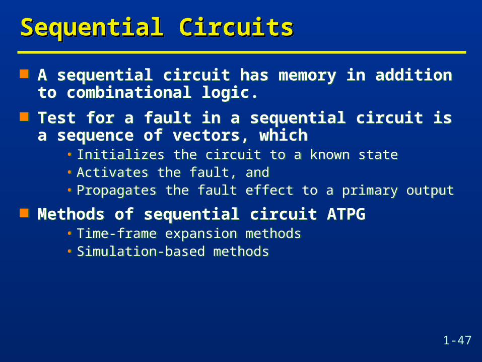
A sequential circuit has memory in addition to combinational logic.
Test for a fault in a sequential circuit is a sequence of vectors, which
• Initializes the circuit to a known state• Activates the fault, and• Propagates the fault effect to a primary output
Methods of sequential circuit ATPG• Time-frame expansion methods• Simulation-based methods

1-48
Example: A Serial AdderExample: A Serial AdderExample: A Serial AdderExample: A Serial Adder
FF
An Bn
Cn Cn+1
Sn
s-a-0
11
1
1
1X
X
X
D
D
Combinational logic

1-49
Time-Frame ExpansionTime-Frame ExpansionTime-Frame ExpansionTime-Frame Expansion
An Bn
FF
Cn Cn+1
1X
X
Sn
s-a-011
1
1
D
D
Combinational logicSn-1
s-a-011
1
1 X
D
D
Combinational logic
Cn-1
1
1
D
D
X
An-1 Bn-1 Time-frame -1 Time-frame 0

1-50
Concept of Time-FramesConcept of Time-FramesConcept of Time-FramesConcept of Time-Frames
If the test sequence for a single stuck-at fault contains n vectors,
• Replicate combinational logic block n times• Place fault in each block• Generate a test for the multiple stuck-at fault using
combinational ATPG with 9-valued logic
If the test sequence for a single stuck-at fault contains n vectors,
• Replicate combinational logic block n times• Place fault in each block• Generate a test for the multiple stuck-at fault using
combinational ATPG with 9-valued logic
Comb.block
Fault
Time-frame
0
Time-frame
-1
Time-frame-n+1
Unknownor given
Init. state
Vector 0Vector -1Vector -n+1
PO 0PO -1PO -n+1
Statevariables
Nextstate

1-51
Example of Sequential CircuitExample of Sequential CircuitExample of Sequential CircuitExample of Sequential Circuit

1-52
Improving Controllability & ObservabilityImproving Controllability & ObservabilityImproving Controllability & ObservabilityImproving Controllability & Observability

1-53
Regular vs. Scan Flip-FlopRegular vs. Scan Flip-FlopRegular vs. Scan Flip-FlopRegular vs. Scan Flip-Flop

1-54
Example Scan Circuit with Scan ChainExample Scan Circuit with Scan ChainExample Scan Circuit with Scan ChainExample Scan Circuit with Scan Chain

1-55
Scan Element OperationsScan Element OperationsScan Element OperationsScan Element Operations
Scan cell provides observability and controllability of the signal path:
Operate: allows normal transparent operation of the element.
Scan Load/Shift: used to serially load/shift data into the scan chain while simultaneously unloading the last sample.
Scan Data Apply: allows the scan element to control the value of the output, thereby controlling the logic driven by Q.
Scan Sample: gives observability of logic that fans into the scan element.

1-56
Scan Test TimingScan Test TimingScan Test TimingScan Test Timing

1-57
Multiple Scan ChainsMultiple Scan ChainsMultiple Scan ChainsMultiple Scan Chains

1-58
Multiple Scan ChainsMultiple Scan ChainsMultiple Scan ChainsMultiple Scan Chains
Using multiple scan chains:• Reduces required tester memory per channel• Reduces test application time

1-59
Stuck-At Scan DiagnosticsStuck-At Scan DiagnosticsStuck-At Scan DiagnosticsStuck-At Scan Diagnostics

1-60
Scan Testing MethodologyScan Testing MethodologyScan Testing MethodologyScan Testing Methodology
Advantages• Direct Controllability & Observability of Internal Nodes
• Enables Combinational ATPG
• More Efficient Vectors
• Higher Potential Fault Coverage
• Deterministic Quality Metric
• Efficient Diagnostic Capability
• AC and DC Compliance
Concerns• Power Consumption
• Clock Skew
• Design Rule Impact on Budgets

1-61
Boundary Scan ArchitectureBoundary Scan ArchitectureBoundary Scan ArchitectureBoundary Scan Architecture

1-62
Built-In Self Test (BIST)Built-In Self Test (BIST)Built-In Self Test (BIST)Built-In Self Test (BIST)
BIST is the capability of a circuit (chip, board, system) to test itself.
BIST architectures consist of• Test pattern generators (TPGs)
• Output response analyzers (ORAs)
• Circuit under test (CUT)
• Distribution system for transmitting data from TPGs to CUTs and from CUTs to ORAs
• BIST controller
BIST is the capability of a circuit (chip, board, system) to test itself.
BIST architectures consist of• Test pattern generators (TPGs)
• Output response analyzers (ORAs)
• Circuit under test (CUT)
• Distribution system for transmitting data from TPGs to CUTs and from CUTs to ORAs
• BIST controller

1-63
Built-In Self Test ExampleBuilt-In Self Test ExampleBuilt-In Self Test ExampleBuilt-In Self Test Example

1-64
Advantages of BISTAdvantages of BISTAdvantages of BISTAdvantages of BIST
Fast, efficient and hierarchical - same hardware is capable of testing chips, boards and systems.
No need of expensive ATE (cost >= $10 milion) Testing during operation and maintenance Uniform technique for production, system and maintenance
tests Dynamic properties of the circuit can be tested at speed Can be used for delay testing as it can be used in real
time

1-65
ConclusionConclusionConclusionConclusion
With increasing design complexity, testing cost has increased dramatically.
Testing must be addressed early in the design process.
Design engineers must have good testing and design for testability knowledge.
Testing introduced in Computer & Electrical Engineering Curriculum in many universities• COE 464: Testing of Digital Circuits
• COE 571: Digital System Testing