coe 571 digital system testing an introduction dr. aiman h. el-maleh computer engineering department...
Post on 20-Dec-2015
216 views
TRANSCRIPT

COE 571COE 571Digital System TestingDigital System Testing
An IntroductionAn Introduction
COE 571COE 571Digital System TestingDigital System Testing
An IntroductionAn Introduction
Dr. Aiman H. El-Maleh
Computer Engineering Department
King Fahd University of Petroleum & Minerals
Dr. Aiman H. El-Maleh
Computer Engineering Department
King Fahd University of Petroleum & Minerals
1-2
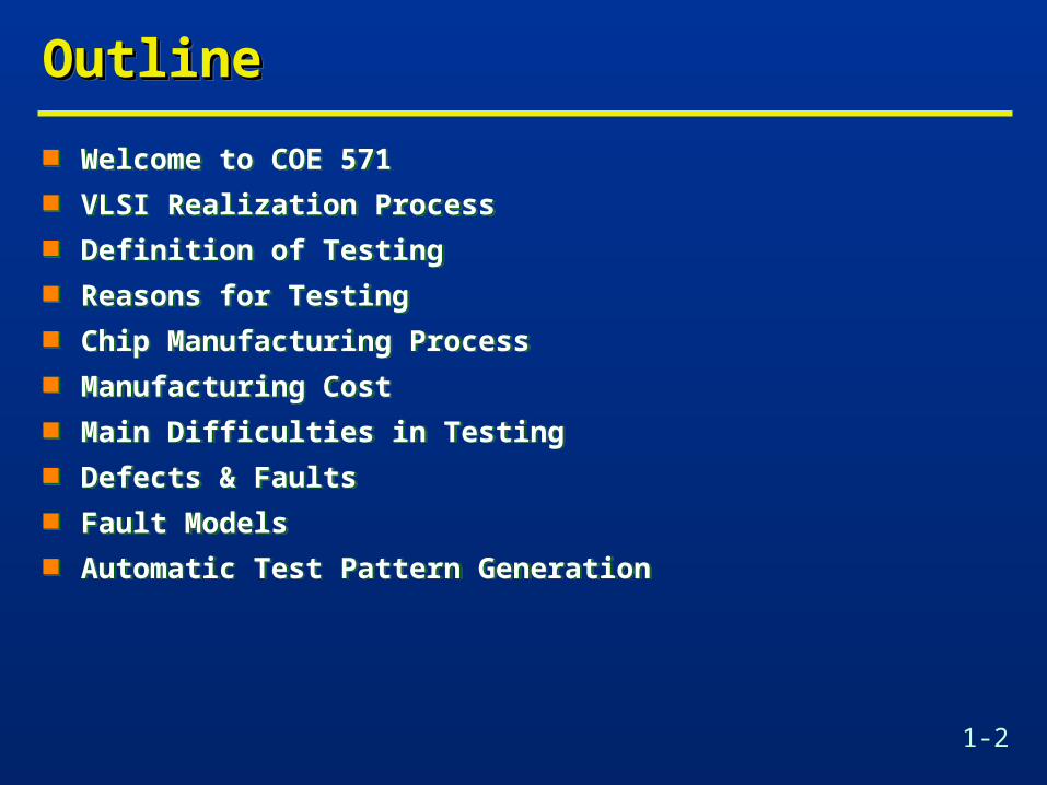
OutlineOutlineOutlineOutline
Welcome to COE 571 VLSI Realization Process Definition of Testing Reasons for Testing Chip Manufacturing Process Manufacturing Cost Main Difficulties in Testing Defects & Faults Fault Models Automatic Test Pattern Generation
Welcome to COE 571 VLSI Realization Process Definition of Testing Reasons for Testing Chip Manufacturing Process Manufacturing Cost Main Difficulties in Testing Defects & Faults Fault Models Automatic Test Pattern Generation
1-3
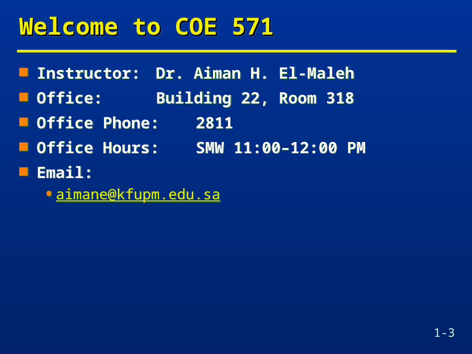
Welcome to COE 571Welcome to COE 571Welcome to COE 571Welcome to COE 571
Instructor:Dr. Aiman H. El-Maleh Office: Building 22, Room 318 Office Phone: 2811 Office Hours: SMW 11:00–12:00 PM Email:
Instructor:Dr. Aiman H. El-Maleh Office: Building 22, Room 318 Office Phone: 2811 Office Hours: SMW 11:00–12:00 PM Email:
1-4
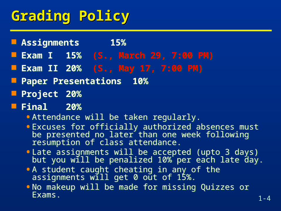
Grading PolicyGrading PolicyGrading PolicyGrading Policy
Assignments 15% Exam I 15% (S., March 29, 7:00 PM) Exam II 20% (S., May 17, 7:00 PM) Paper Presentations 10% Project 20% Final 20%
• Attendance will be taken regularly.• Excuses for officially authorized absences must be presented
no later than one week following resumption of class attendance.
• Late assignments will be accepted (upto 3 days) but you will be penalized 10% per each late day.
• A student caught cheating in any of the assignments will get 0 out of 15%.
• No makeup will be made for missing Quizzes or Exams.
1-5
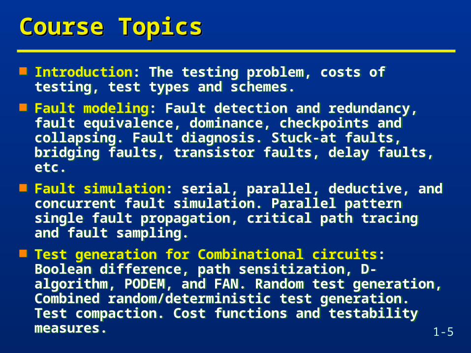
Course TopicsCourse TopicsCourse TopicsCourse Topics
Introduction: The testing problem, costs of testing, test types and schemes.
Fault modeling: Fault detection and redundancy, fault equivalence, dominance, checkpoints and collapsing. Fault diagnosis. Stuck-at faults, bridging faults, transistor faults, delay faults, etc.
Fault simulation: serial, parallel, deductive, and concurrent fault simulation. Parallel pattern single fault propagation, critical path tracing and fault sampling.
Test generation for Combinational circuits: Boolean difference, path sensitization, D-algorithm, PODEM, and FAN. Random test generation, Combined random/deterministic test generation. Test compaction. Cost functions and testability measures.
1-6
Course TopicsCourse TopicsCourse TopicsCourse Topics
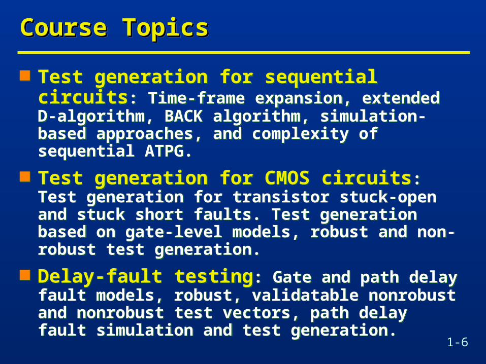
Test generation for sequential circuits: Time-frame expansion, extended D-algorithm, BACK algorithm, simulation-based approaches, and complexity of sequential ATPG.
Test generation for CMOS circuits: Test generation for transistor stuck-open and stuck short faults. Test generation based on gate-level models, robust and non-robust test generation.
Delay-fault testing: Gate and path delay fault models, robust, validatable nonrobust and nonrobust test vectors, path delay fault simulation and test generation.
1-7
Course TopicsCourse TopicsCourse TopicsCourse Topics
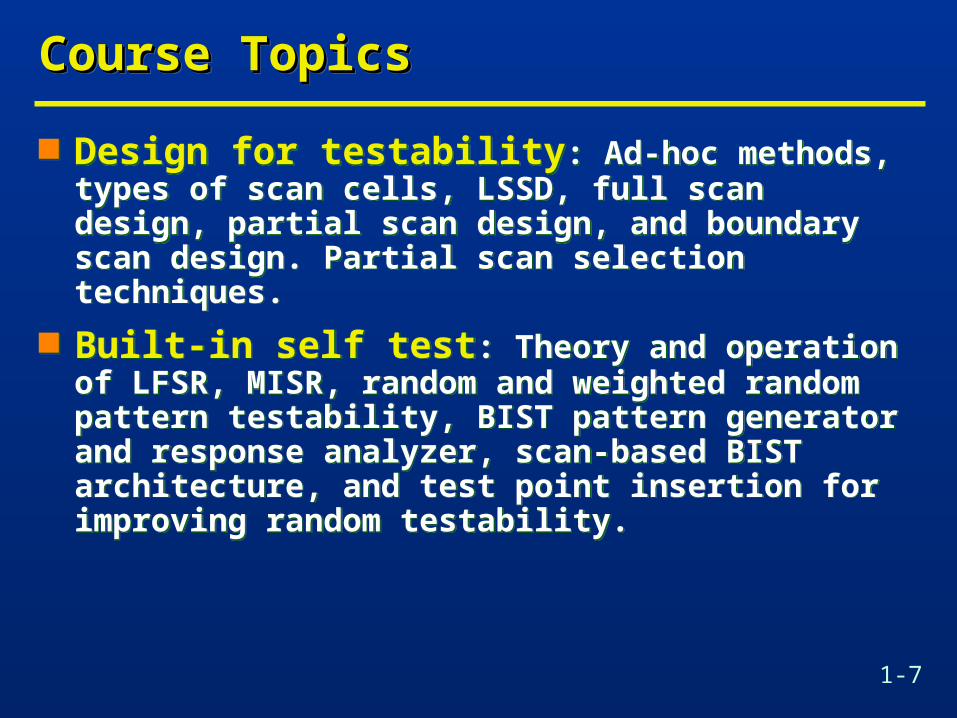
Design for testability: Ad-hoc methods, types of scan cells, LSSD, full scan design, partial scan design, and boundary scan design. Partial scan selection techniques.
Built-in self test: Theory and operation of LFSR, MISR, random and weighted random pattern testability, BIST pattern generator and response analyzer, scan-based BIST architecture, and test point insertion for improving random testability.
1-8
TextbookTextbookTextbookTextbook
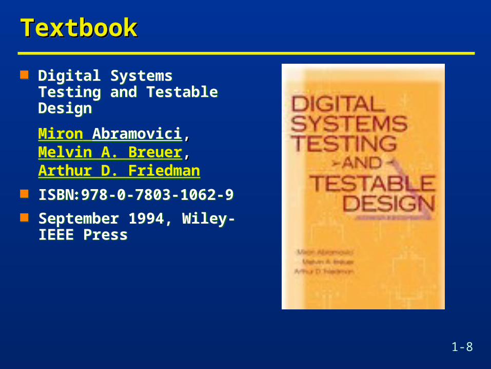
Digital Systems Testing and Testable Design
Miron Abramovici, , Melvin A. Breuer, , Arthur D. Friedman
ISBN: 978-0-7803-1062-9 September 1994, Wiley-
IEEE Press
Digital Systems Testing and Testable Design
Miron Abramovici, , Melvin A. Breuer, , Arthur D. Friedman
ISBN: 978-0-7803-1062-9 September 1994, Wiley-
IEEE Press
1-9
VLSI Realization ProcessVLSI Realization ProcessVLSI Realization ProcessVLSI Realization Process
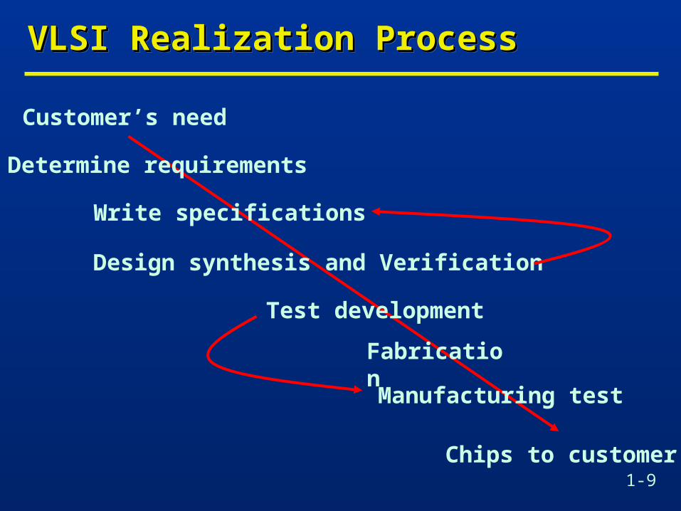
Determine requirements
Write specifications
Design synthesis and Verification
FabricationManufacturing test
Chips to customer
Customer’s need
Test development
1-10
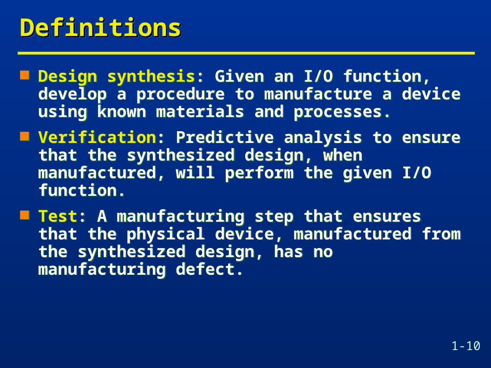
DefinitionsDefinitionsDefinitionsDefinitions
Design synthesis: Given an I/O function, develop a procedure to manufacture a device using known materials and processes.
Verification: Predictive analysis to ensure that the synthesized design, when manufactured, will perform the given I/O function.
Test: A manufacturing step that ensures that the physical device, manufactured from the synthesized design, has no manufacturing defect.
1-11
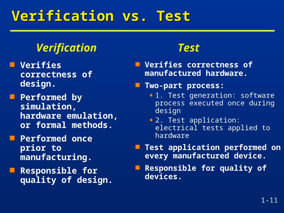
Verification vs. TestVerification vs. TestVerification vs. TestVerification vs. Test
Verifies correctness of design.
Performed by simulation, hardware emulation, or formal methods.
Performed once prior to manufacturing.
Responsible for quality of design.
Verifies correctness of manufactured hardware.
Two-part process:• 1. Test generation: software
process executed once during design
• 2. Test application: electrical tests applied to hardware
Test application performed on every manufactured device.
Responsible for quality of devices.
Verification Test
1-12
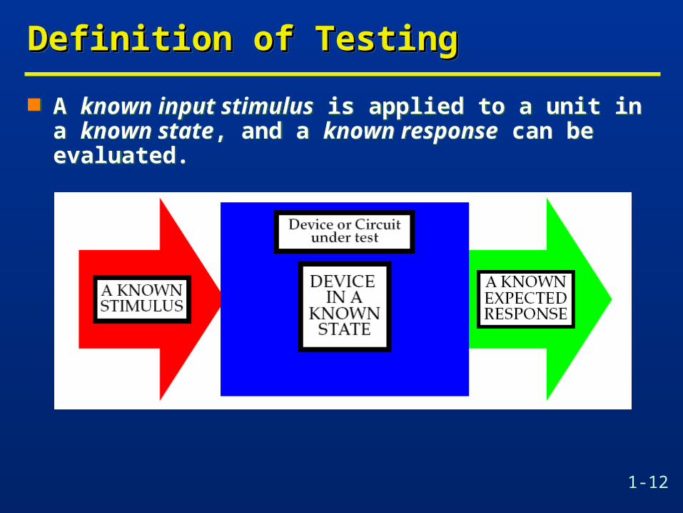
Definition of TestingDefinition of TestingDefinition of TestingDefinition of Testing
A known input stimulus is applied to a unit in a known state, and a known response can be evaluated.
A known input stimulus is applied to a unit in a known state, and a known response can be evaluated.
1-13
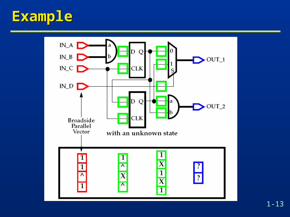
ExampleExampleExampleExample
1-14
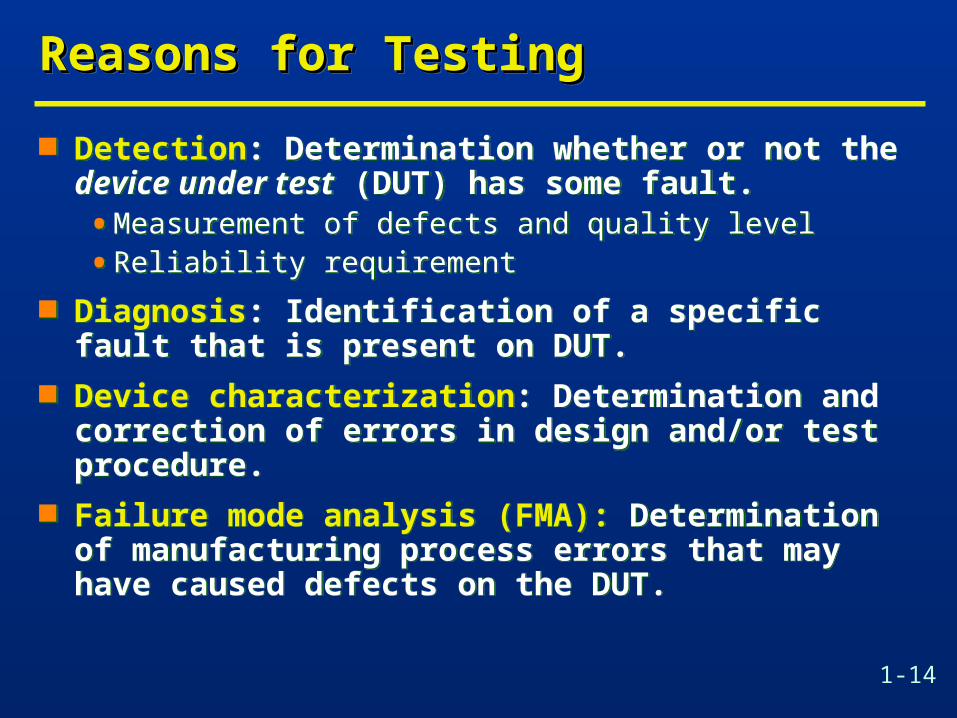
Reasons for TestingReasons for TestingReasons for TestingReasons for Testing
Detection: Determination whether or not the device under test (DUT) has some fault.• Measurement of defects and quality level
• Reliability requirement
Diagnosis: Identification of a specific fault that is present on DUT.
Device characterization: Determination and correction of errors in design and/or test procedure.
Failure mode analysis (FMA): Determination of manufacturing process errors that may have caused defects on the DUT.
1-15
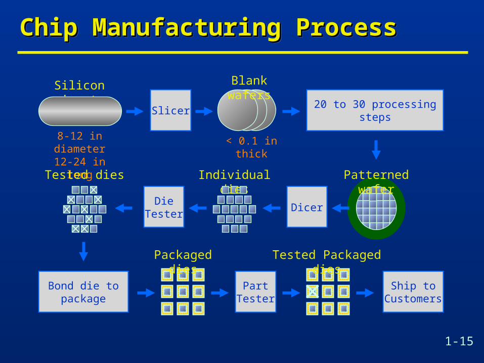
Chip Manufacturing ProcessChip Manufacturing ProcessChip Manufacturing ProcessChip Manufacturing Process
Silicon ingot
Slicer
Blank wafers
20 to 30 processing steps
8-12 in diameter12-24 in long
< 0.1 in thick
Patterned wafer
Dicer
Individual dies
DieTester
Tested dies
Bond die topackage
Packaged dies
PartTester
Tested Packaged dies
Ship toCustomers
1-16
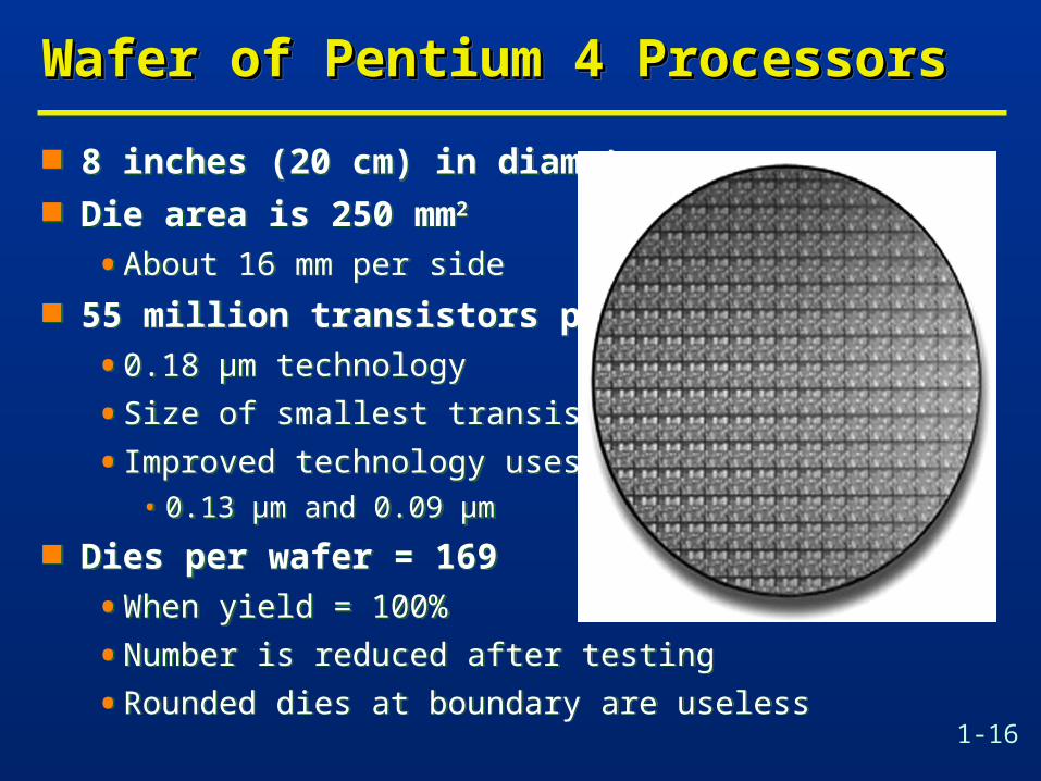
Wafer of Pentium 4 ProcessorsWafer of Pentium 4 ProcessorsWafer of Pentium 4 ProcessorsWafer of Pentium 4 Processors
8 inches (20 cm) in diameter Die area is 250 mm2
• About 16 mm per side
55 million transistors per die
• 0.18 μm technology
• Size of smallest transistor
• Improved technology uses• 0.13 μm and 0.09 μm
Dies per wafer = 169
• When yield = 100%
• Number is reduced after testing
• Rounded dies at boundary are useless
1-17
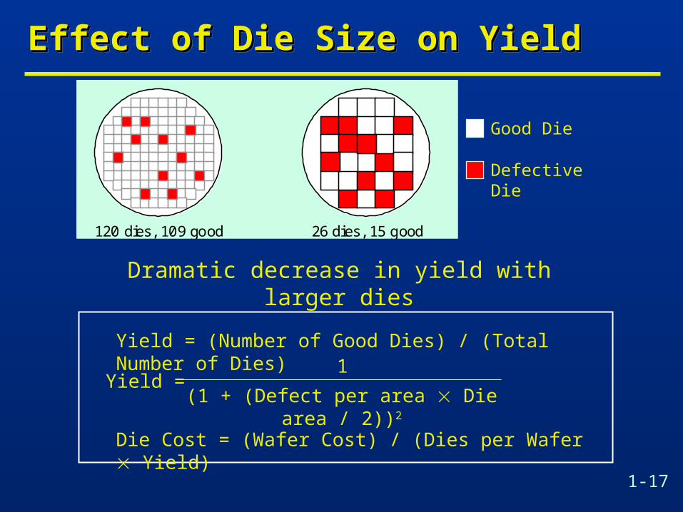
Effect of Die Size on YieldEffect of Die Size on YieldEffect of Die Size on YieldEffect of Die Size on Yield
Dramatic decrease in yield with larger dies
Yield = (Number of Good Dies) / (Total Number of Dies)
Defective Die
Good Die
120 dies, 109 good 26 dies, 15 good
(1 + (Defect per area Die area / 2))2
1Yield =
Die Cost = (Wafer Cost) / (Dies per Wafer Yield)
1-18
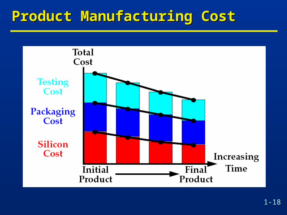
Product Manufacturing CostProduct Manufacturing CostProduct Manufacturing CostProduct Manufacturing Cost
1-19
Product Manufacturing CostProduct Manufacturing CostProduct Manufacturing CostProduct Manufacturing Cost
Reduction of silicon cost • increasing volume and yield
• die size reduction (process shrinks or more efficient layout)
Reduction of packaging cost • increasing volume
• shifting to lower cost packages if possible (e.g., from ceramic to plastic)
• reduction in package pin count
Reduction in cost of test • reducing vector data size
• reducing the cost of the tester
• reducing test time

1-20
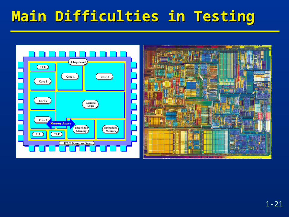
Main Difficulties in TestingMain Difficulties in TestingMain Difficulties in TestingMain Difficulties in Testing
Miniaturization Physical access difficult or impossible.
Increasing complexity Large amount of test data.
Number of access ports remains constant Long test application time.
High speed High demand on tester’s driver/sensor mechanism and more complicated failure mechanism.
Testing accounts up to 50% of product development efforts.
The key to successful testing lies in the design process.
1-21
Main Difficulties in TestingMain Difficulties in TestingMain Difficulties in TestingMain Difficulties in Testing
1-22
Costs of TestingCosts of TestingCosts of TestingCosts of Testing
Design for testability (DFT)• Chip area overhead and yield reduction
• Performance overhead
Software processes of test• Test generation and fault simulation
• Test programming and debugging
Manufacturing test• Automatic test equipment (ATE) capital cost
• Test center operational cost
Design for testability (DFT)• Chip area overhead and yield reduction
• Performance overhead
Software processes of test• Test generation and fault simulation
• Test programming and debugging
Manufacturing test• Automatic test equipment (ATE) capital cost
• Test center operational cost
1-23
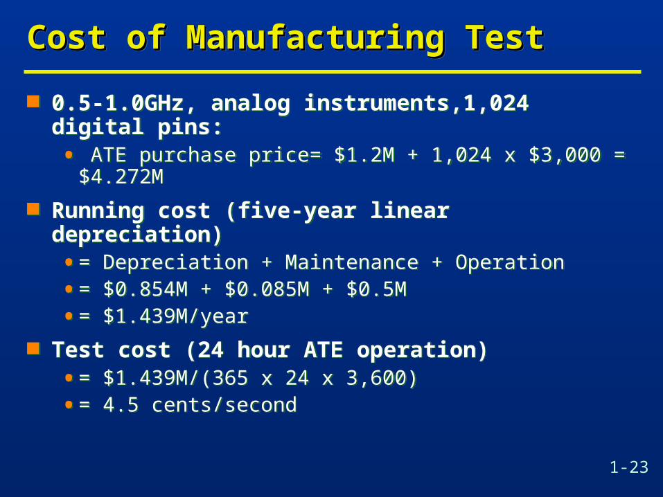
Cost of Manufacturing TestCost of Manufacturing TestCost of Manufacturing TestCost of Manufacturing Test
0.5-1.0GHz, analog instruments,1,024 digital pins:• ATE purchase price= $1.2M + 1,024 x $3,000 = $4.272M
Running cost (five-year linear depreciation)• = Depreciation + Maintenance + Operation
• = $0.854M + $0.085M + $0.5M
• = $1.439M/year
Test cost (24 hour ATE operation)• = $1.439M/(365 x 24 x 3,600)
• = 4.5 cents/second
1-24
Automatic Test Equipment ComponentsAutomatic Test Equipment ComponentsAutomatic Test Equipment ComponentsAutomatic Test Equipment Components
Powerful computer Powerful 32-bit Digital Signal Processor (DSP) for
analog testing Test Program (written in high-level language) running
on the computer Probe Head (actually touches the bare or packaged
chip to perform fault detection experiments) Probe Card or Membrane Probe (contains electronics
to measure signals on chip pin or pad)
1-25
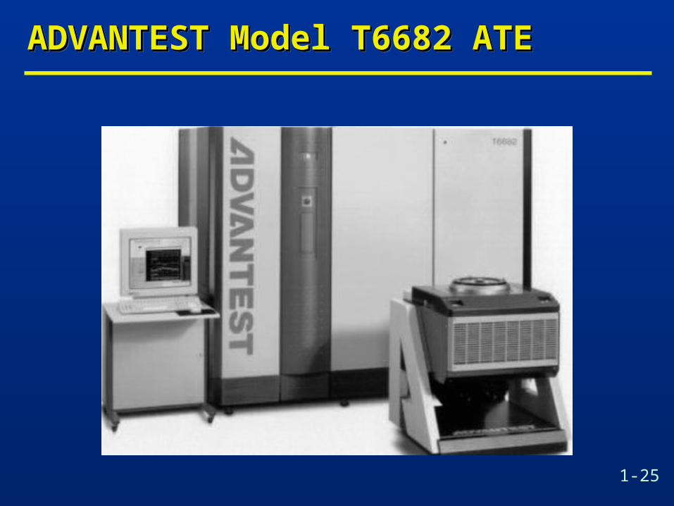
ADVANTEST Model T6682 ATEADVANTEST Model T6682 ATEADVANTEST Model T6682 ATEADVANTEST Model T6682 ATE
1-26
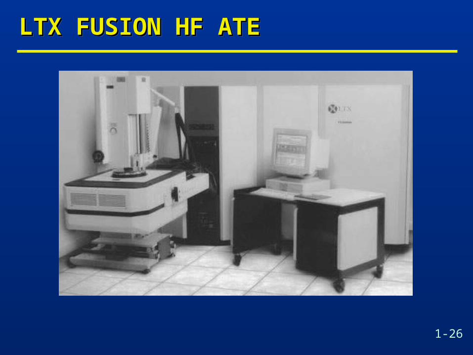
LTX FUSION HF ATELTX FUSION HF ATELTX FUSION HF ATELTX FUSION HF ATE
1-27
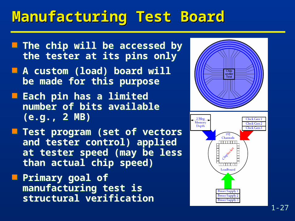
Manufacturing Test BoardManufacturing Test BoardManufacturing Test BoardManufacturing Test Board
The chip will be accessed by the tester at its pins only
A custom (load) board will be made for this purpose
Each pin has a limited number of bits available (e.g., 2 MB)
Test program (set of vectors and tester control) applied at tester speed (may be less than actual chip speed)
Primary goal of manufacturing test is structural verification
1-28
Design For TestabilityDesign For TestabilityDesign For TestabilityDesign For Testability
To take into account the testing aspects during the design process so that more testable designs will be generated.
Advantages of DFT• Reduce test efforts.
• Eases generation of test vectors• Eases diagnosis & debugging
• Reduce cost for test equipments (ATE).
• Shorten turnaround time.
• Increase product quality.
Disadvantages of DFT• Adds complexity to design methodology
• Impacts design area, power, speed and package pins
1-29
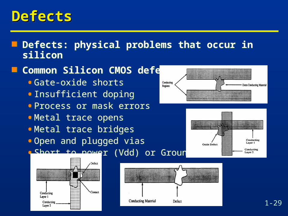
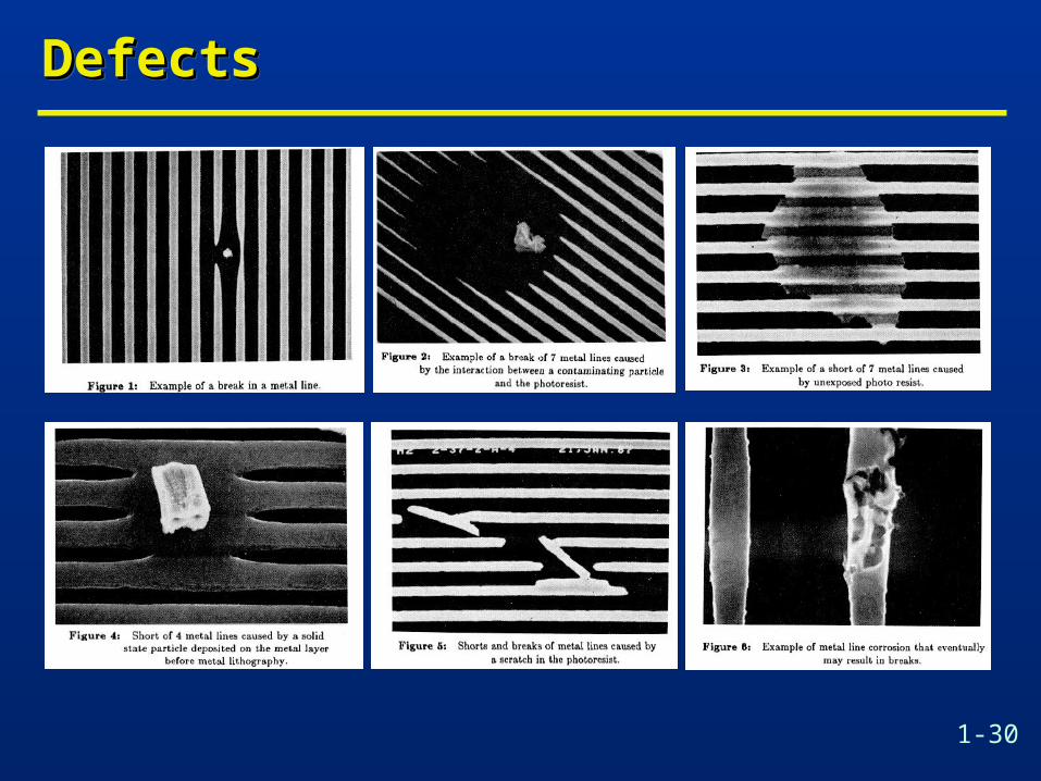
DefectsDefectsDefectsDefects
Defects: physical problems that occur in silicon Common Silicon CMOS defects:
• Gate-oxide shorts
• Insufficient doping
• Process or mask errors
• Metal trace opens
• Metal trace bridges
• Open and plugged vias
• Short to power (Vdd) or Ground (Vss)
Defects: physical problems that occur in silicon Common Silicon CMOS defects:
• Gate-oxide shorts
• Insufficient doping
• Process or mask errors
• Metal trace opens
• Metal trace bridges
• Open and plugged vias
• Short to power (Vdd) or Ground (Vss)
1-30
DefectsDefectsDefectsDefects
1-31
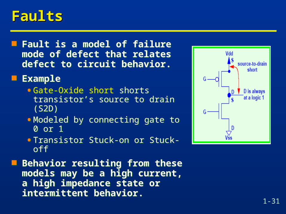
FaultsFaultsFaultsFaults
Fault is a model of failure mode of defect that relates defect to circuit behavior.
Example• Gate-Oxide short shorts transistor’s
source to drain (S2D)
• Modeled by connecting gate to 0 or 1
• Transistor Stuck-on or Stuck-off
Behavior resulting from these models may be a high current, a high impedance state or intermittent behavior.
1-32
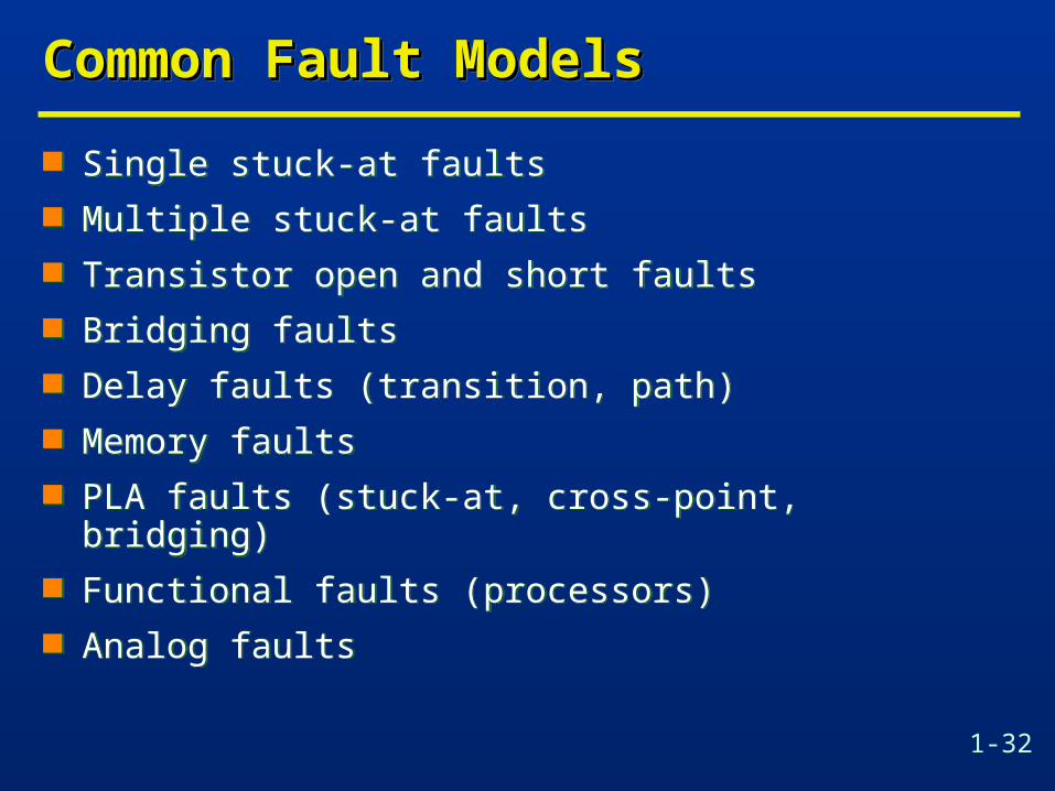
Common Fault ModelsCommon Fault ModelsCommon Fault ModelsCommon Fault Models
Single stuck-at faults Multiple stuck-at faults Transistor open and short faults Bridging faults Delay faults (transition, path) Memory faults PLA faults (stuck-at, cross-point, bridging) Functional faults (processors) Analog faults
Single stuck-at faults Multiple stuck-at faults Transistor open and short faults Bridging faults Delay faults (transition, path) Memory faults PLA faults (stuck-at, cross-point, bridging) Functional faults (processors) Analog faults
1-33
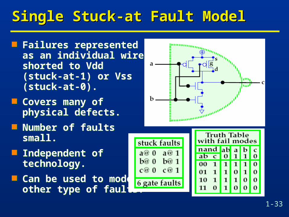
Single Stuck-at Fault ModelSingle Stuck-at Fault ModelSingle Stuck-at Fault ModelSingle Stuck-at Fault Model
Failures represented as an individual wire shorted to Vdd (stuck-at-1) or Vss (stuck-at-0).
Covers many of physical defects.
Number of faults small. Independent of
technology. Can be used to model
other type of faults.
Failures represented as an individual wire shorted to Vdd (stuck-at-1) or Vss (stuck-at-0).
Covers many of physical defects.
Number of faults small. Independent of
technology. Can be used to model
other type of faults.
1-34
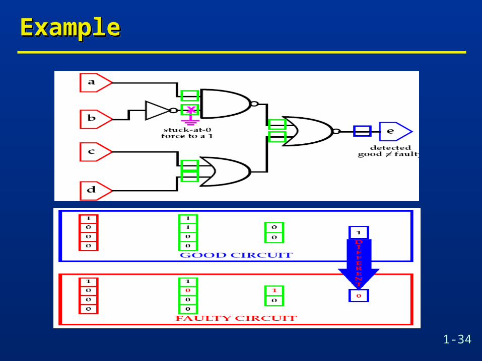
ExampleExampleExampleExample
1-35
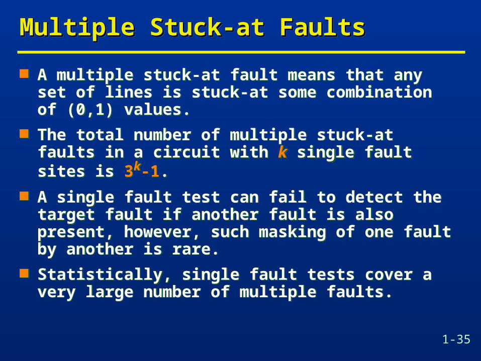
Multiple Stuck-at FaultsMultiple Stuck-at FaultsMultiple Stuck-at FaultsMultiple Stuck-at Faults
A multiple stuck-at fault means that any set of lines is stuck-at some combination of (0,1) values.
The total number of multiple stuck-at faults in a circuit with k single fault sites is 3k-1.
A single fault test can fail to detect the target fault if another fault is also present, however, such masking of one fault by another is rare.
Statistically, single fault tests cover a very large number of multiple faults.
1-36
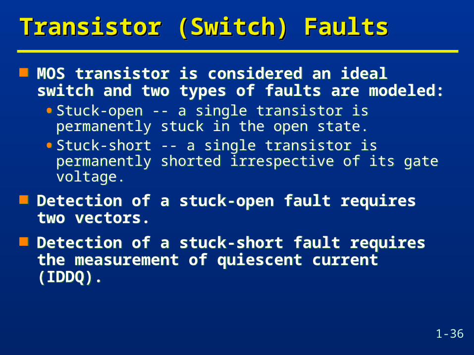
Transistor (Switch) FaultsTransistor (Switch) FaultsTransistor (Switch) FaultsTransistor (Switch) Faults
MOS transistor is considered an ideal switch and two types of faults are modeled:• Stuck-open -- a single transistor is permanently stuck in the
open state.
• Stuck-short -- a single transistor is permanently shorted irrespective of its gate voltage.
Detection of a stuck-open fault requires two vectors. Detection of a stuck-short fault requires the
measurement of quiescent current (IDDQ).
1-37
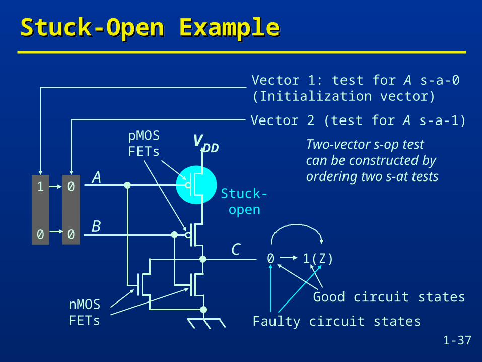
Stuck-Open ExampleStuck-Open ExampleStuck-Open ExampleStuck-Open Example
Two-vector s-op testcan be constructed byordering two s-at testsA
B
VDD
C
pMOSFETs
nMOSFETs
Stuck-open
1
0
0
0
0 1(Z)
Good circuit states
Faulty circuit states
Vector 1: test for A s-a-0(Initialization vector)
Vector 2 (test for A s-a-1)
1-38
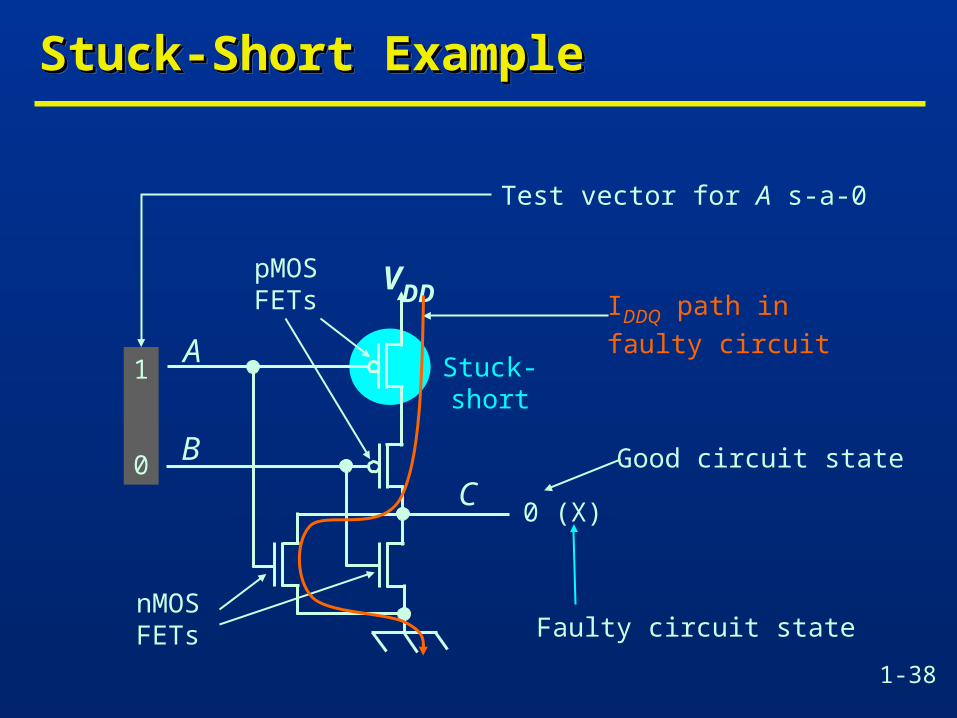
Stuck-Short ExampleStuck-Short ExampleStuck-Short ExampleStuck-Short Example
A
B
VDD
C
pMOSFETs
nMOSFETs
Stuck-short
1
0
0 (X)
Good circuit state
Faulty circuit state
Test vector for A s-a-0
IDDQ path infaulty circuit
1-39
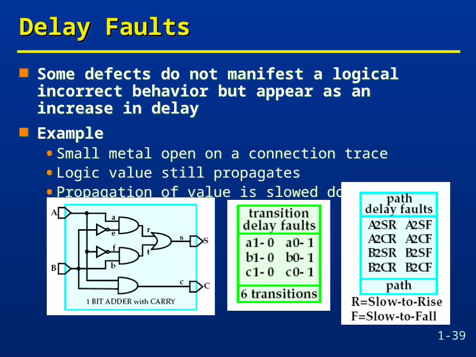
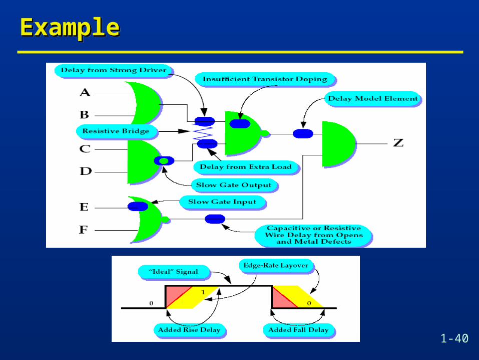
Delay FaultsDelay FaultsDelay FaultsDelay Faults
Some defects do not manifest a logical incorrect behavior but appear as an increase in delay
Example• Small metal open on a connection trace
• Logic value still propagates
• Propagation of value is slowed down
Some defects do not manifest a logical incorrect behavior but appear as an increase in delay
Example• Small metal open on a connection trace
• Logic value still propagates
• Propagation of value is slowed down
1-40
ExampleExampleExampleExample
1-41
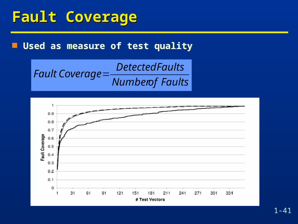
Fault CoverageFault CoverageFault CoverageFault Coverage
Used as measure of test quality Used as measure of test quality
FaultsofNumber
FaultsDetectedCoverageFault
1-42
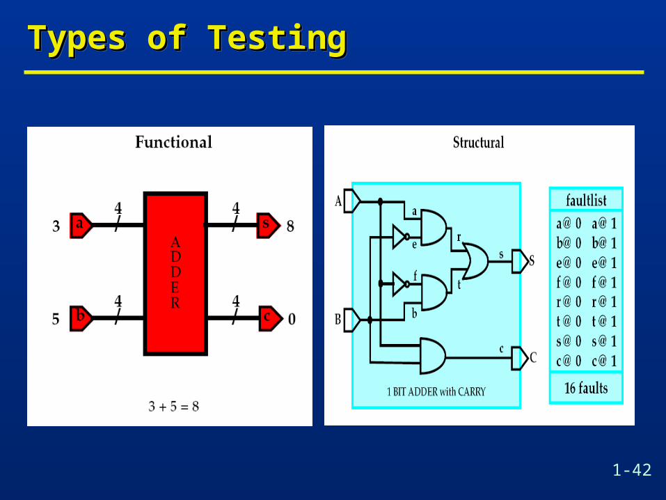
Types of TestingTypes of TestingTypes of TestingTypes of Testing
1-43
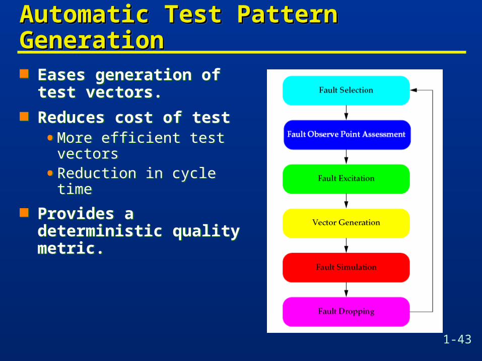
Automatic Test Pattern Generation Automatic Test Pattern Generation Automatic Test Pattern Generation Automatic Test Pattern Generation
Eases generation of test vectors.
Reduces cost of test • More efficient test vectors
• Reduction in cycle time
Provides a deterministic quality metric.
Eases generation of test vectors.
Reduces cost of test • More efficient test vectors
• Reduction in cycle time
Provides a deterministic quality metric.
1-44
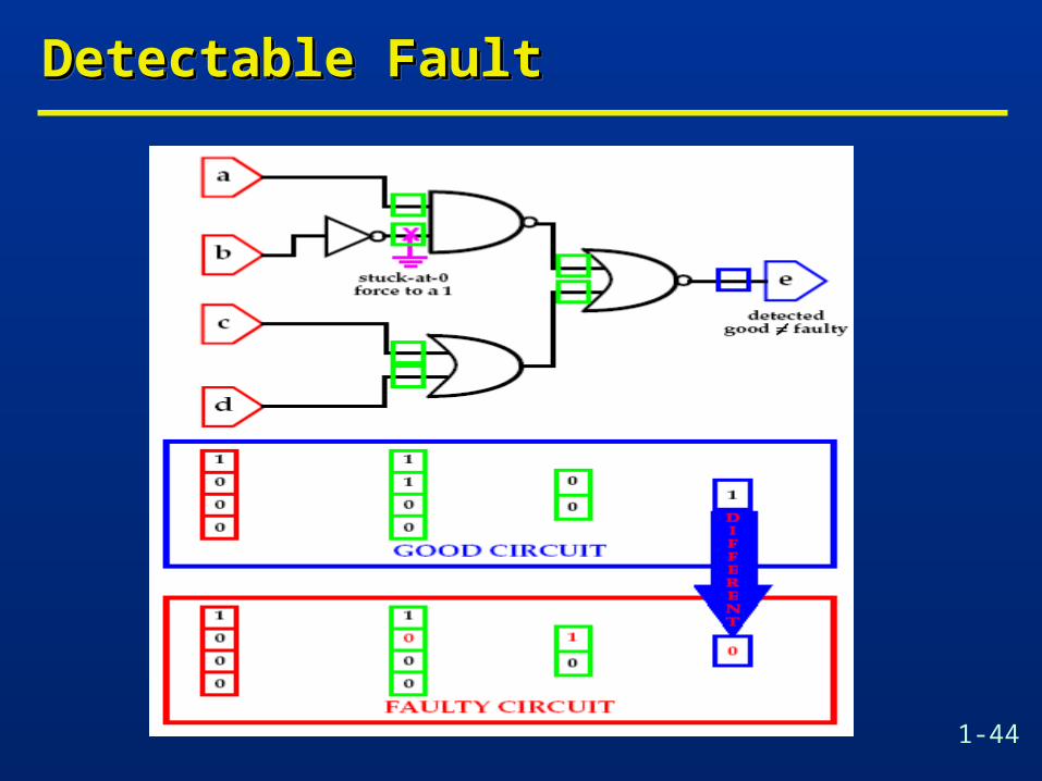
Detectable FaultDetectable FaultDetectable FaultDetectable Fault
1-45
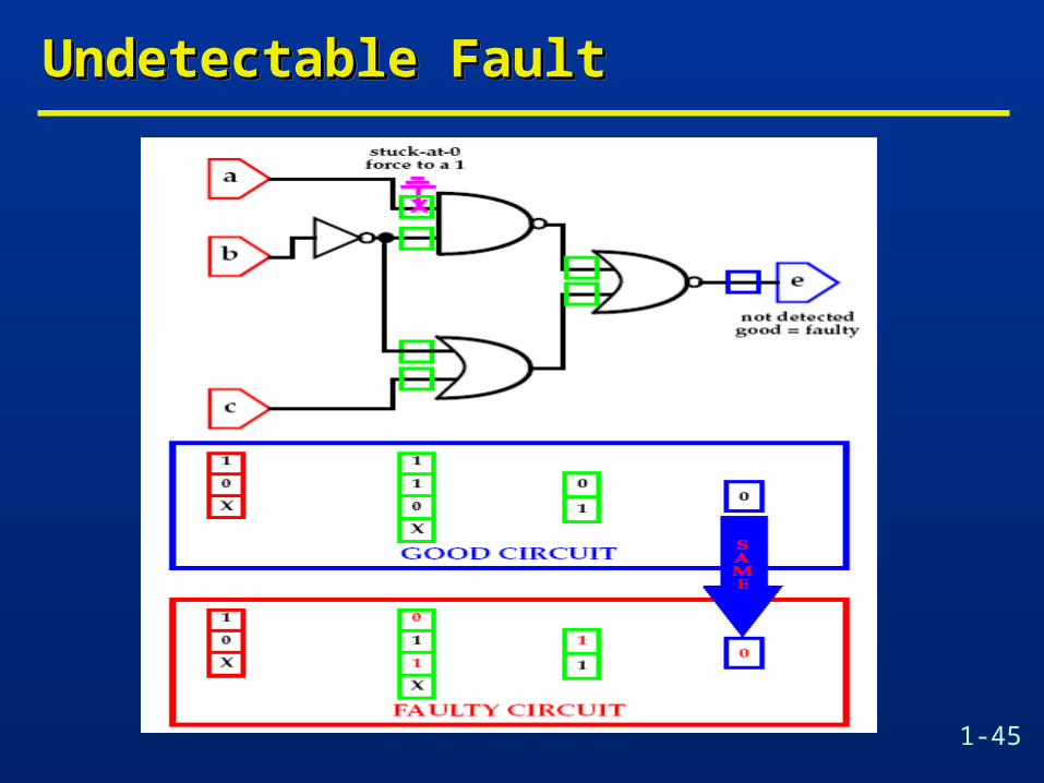
Undetectable FaultUndetectable FaultUndetectable FaultUndetectable Fault