the architecture of the intel® pxa800f cellular · pdf filezarchitecture/design challenges...
TRANSCRIPT
®®
The Architecture of the Intel
®PXA800F Cellular Processor
Dilip Krishnaswamy
Wireless Communications and Computing Group
Intel Corporation
PCA Components Group
®®
Agenda
Architecture/Design Challenges
GSM/GPRS overview
Chip overview
Architectural Features
Reference Designs
Performance Results
Summary

®®
Arch/Design ChallengesDevelop a high-performance low power embedded SoC arch with integrated memories for a GSM/GPRS phone
Take advantage of small protocol code size requirements
Integrate Flash memory (reprogrammable) into the chip
– Lower latencies/higher perf with integrated memory
– Consider options to keep memory closer to processors
– Choose memory size sufficient for comm and apps
Develop a new 0.13 Flash+Logic process
Address leakage concerns with the 0.13u process to obtain good standby time for such a phone
Have good performance for comm and apps sub-systems
Optimize vectors such as performance, power, area, latencies, cost, energy/battery life, system efficiency

®®
Agenda
Architecture/Design Challenges
GSM/GPRS overview
Chip overview
Architectural Features
Reference Designs
Performance Results
Summary

®®
The GSM/GPRS StandardMost widely-used standard in the cellular industry
850MHz, 900MHz, 1800MHz, 1900MHz bands
TDMA with 8-slotted users in 200kHz channels
– Time slot is of 577us duration
GSM standard for Voice
– Different frequency channels Rx and Tx
– One time slot each for Rx and Tx
GPRS standard for Data
– Class 12 phone (4Rx + 1 Tx, 3Rx + 2Tx, 2Rx + 3Tx, 1Rx + 4Tx)
Link adaptation used to switch between modulation and coding schemes depending on channel conditions

®®
Agenda
Architecture/Design Challenges
GSM/GPRS overview
Chip Overview
Architectural Features
Reference Designs
Performance Results
Summary
®®
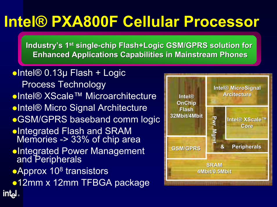
Intel® PXA800F Cellular Processor
Industry’s 1Industry’s 1stst singlesingle--chip Flash+Logic GSM/GPRS solution forchip Flash+Logic GSM/GPRS solution for
Enhanced Applications Capabilities in Mainstream PhonesEnhanced Applications Capabilities in Mainstream Phones
Intel® 0.13µ Flash + Logic
Process Technology
Intel® XScale™ Microarchitecture
Intel® Micro Signal Architecture
GSM/GPRS baseband comm logic
Integrated Flash and SRAM Memories -> 33% of chip area
Integrated Power Management and Peripherals
Approx 108 transistors
12mm x 12mm TFBGA package
Intel®Intel®
OnChipOnChip
FlashFlash
32Mbit/4Mbit32Mbit/4Mbit
Intel® MicroSignalIntel® MicroSignal
ArcitectureArcitecture
Intel® XScale™Intel® XScale™
CoreCore
& Peripherals& Peripherals
SRAMSRAM
4Mbit/0.5Mbit4Mbit/0.5Mbit
Pw
r. Mg
mt.
Pw
r. Mg
mt.
GSM/GPRSGSM/GPRS
®®
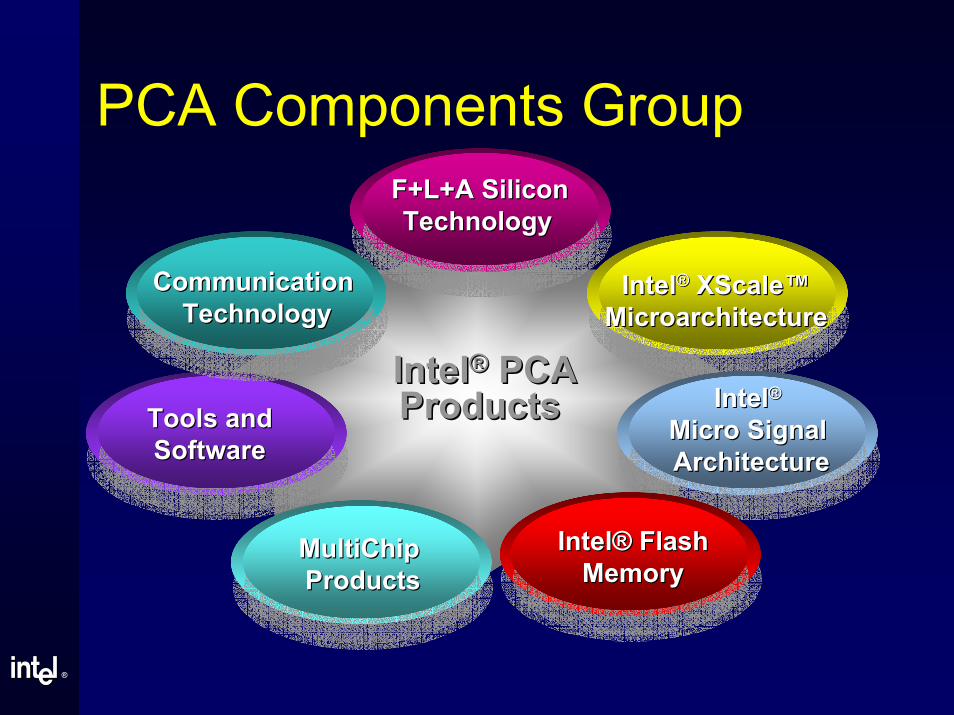
PCA Components Group
F+L+A SiliconF+L+A Silicon
TechnologyTechnology
IntelIntel®® XScale™XScale™
MicroarchitectureMicroarchitecture
IntelIntel®®
Micro Signal Micro Signal
ArchitectureArchitecture
Intel® Flash Intel® Flash
MemoryMemory
IntelIntel®® PCAPCAProducts Products Tools andTools and
SoftwareSoftware
Communication Communication
TechnologyTechnology
MultiChip MultiChip
ProductsProducts

®®
Intel® PXA800F Cellular Processor:Intel® PXA800F Cellular Processor:2.5G GSM/ GPRS Class 122.5G GSM/ GPRS Class 12
Complete Integrated baseband
solution
Intel® XScale™ Microarchitecture
ARM* V5TE compliant
Intel® Micro Signal Architecture
Modified Harvard Architecture
36 Mb integrated Intel® OnChip Flash memory
4.5 Mb integrated SRAM memory
Total solution
Full GSM/GPRS Class 12
L1-L3 Comm protocol software
RTOS Java-based platform
API for customer apps development
Designed for use with industry-
proven mixed signal/RF solutions
Optimized PowerMgmt IC (Dialog)
Handset reference design (Elektrobit)
Intel® Micro
Signal
Architecture
GSM/GPRS Logic
Intel® PXA800FCellular Processor
Intel® OnChip
Flash
32Mbit
SRAM
4Mbit
Peripherals
Intel®
XScale™ Core
RXTX
Analog
Mixed Signal
RF
Transceiver
Dialog Power
Management
Keypad
3
6
9
2
5
8
1
4
7
#0*
Display SIM
Intel® OnChip
Flash
4Mbit
SRAM
512Kbit
*Other names and brands are the property of their respective owners

®®
Key Modules in the Chip
®®
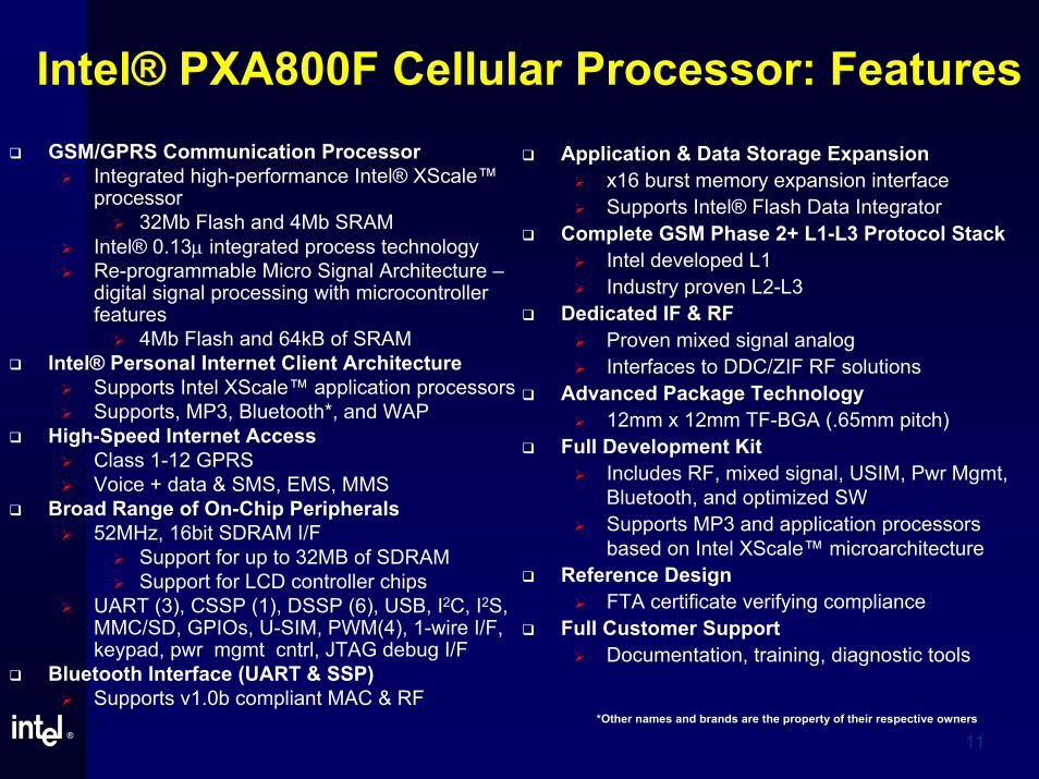
Intel® PXA800F Cellular Processor: Features
GSM/GPRS Communication Processor
Integrated high-performance Intel® XScale™ processor
32Mb Flash and 4Mb SRAM
Intel® 0.13µ integrated process technology
Re-programmable Micro Signal Architecture –digital signal processing with microcontroller features
4Mb Flash and 64kB of SRAM
Intel® Personal Internet Client Architecture
Supports Intel XScale™ application processors
Supports, MP3, Bluetooth*, and WAP
High-Speed Internet Access
Class 1-12 GPRS
Voice + data & SMS, EMS, MMS
Broad Range of On-Chip Peripherals
52MHz, 16bit SDRAM I/F
Support for up to 32MB of SDRAM
Support for LCD controller chips
UART (3), CSSP (1), DSSP (6), USB, I2C, I2S, MMC/SD, GPIOs, U-SIM, PWM(4), 1-wire I/F, keypad, pwr mgmt cntrl, JTAG debug I/F
Bluetooth Interface (UART & SSP)
Supports v1.0b compliant MAC & RF
Application & Data Storage Expansion
x16 burst memory expansion interface
Supports Intel® Flash Data Integrator
Complete GSM Phase 2+ L1-L3 Protocol Stack
Intel developed L1
Industry proven L2-L3
Dedicated IF & RF
Proven mixed signal analog
Interfaces to DDC/ZIF RF solutions
Advanced Package Technology
12mm x 12mm TF-BGA (.65mm pitch)
Full Development Kit
Includes RF, mixed signal, USIM, Pwr Mgmt,
Bluetooth, and optimized SW
Supports MP3 and application processors
based on Intel XScale™ microarchitecture
Reference Design
FTA certificate verifying compliance
Full Customer Support
Documentation, training, diagnostic tools
*Other names and brands are the property of their respective owners
11

®®
Agenda
Architecture/Design Challenges
GSM/GPRS overview
Chip Overview
Architectural Features
Reference Designs
Performance Results
Summary
®®
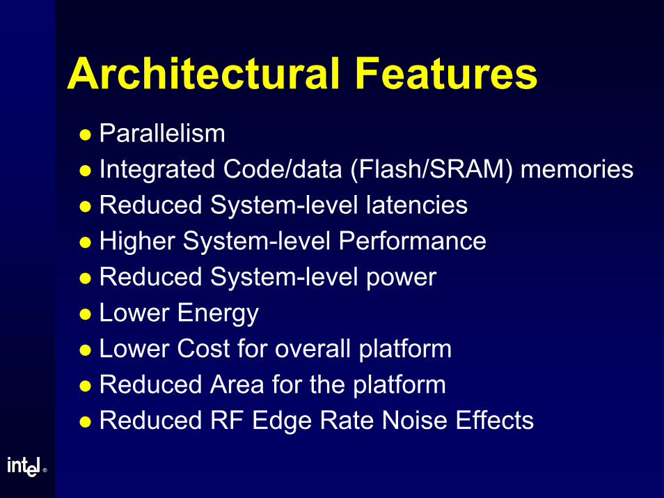
Architectural Features
Parallelism
Integrated Code/data (Flash/SRAM) memories
Reduced System-level latencies
Higher System-level Performance
Reduced System-level power
Lower Energy
Lower Cost for overall platform
Reduced Area for the platform
Reduced RF Edge Rate Noise Effects
®®
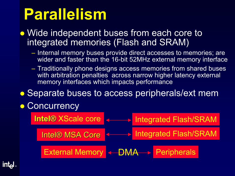
ParallelismWide independent buses from each core to integrated memories (Flash and SRAM)
– Internal memory buses provide direct accesses to memories; are wider and faster than the 16-bit 52MHz external memory interface
– Traditionally phone designs access memories from shared buses with arbitration penalties across narrow higher latency external memory interfaces which impacts performance
Separate buses to access peripherals/ext mem
Concurrency
Intel® MSA CoreIntel® MSA Core
External Memory Peripherals
Integrated Flash/SRAM
Integrated Flash/SRAMIntel®Intel® XScale core
DMA
®®
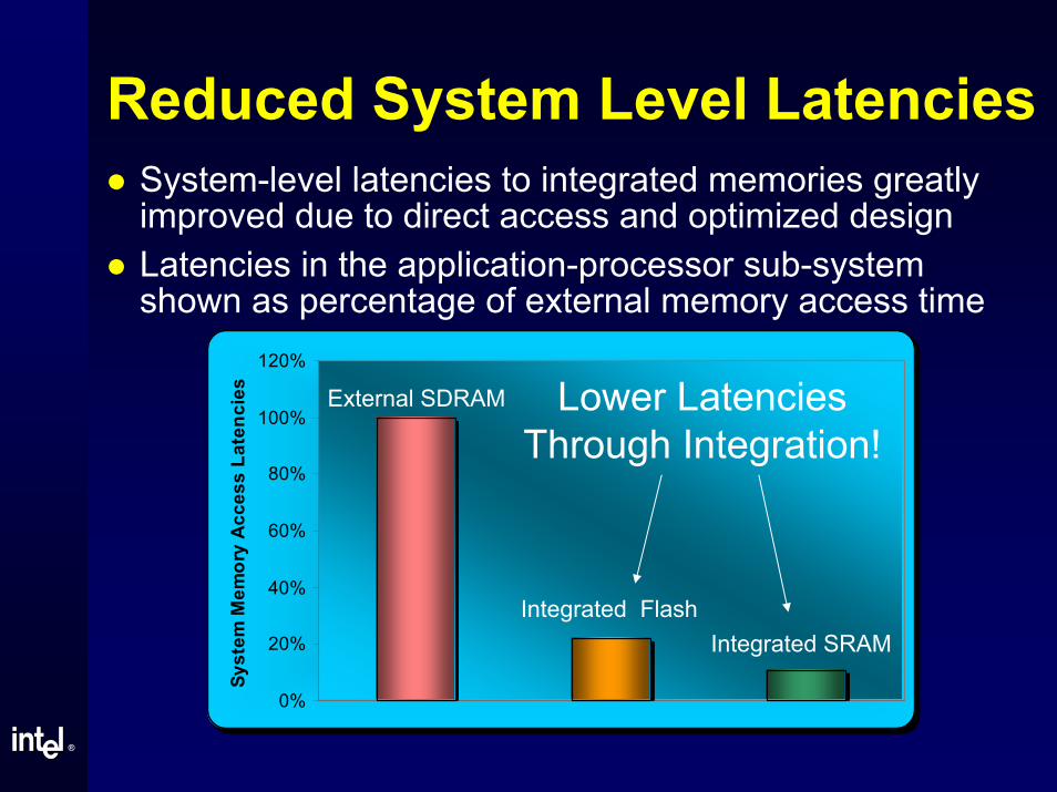
Reduced System Level Latencies
System-level latencies to integrated memories greatly improved due to direct access and optimized design
Latencies in the application-processor sub-system shown as percentage of external memory access time
0%
20%
40%
60%
80%
100%
120%
Sy
ste
m M
em
ory
Ac
ce
ss
La
ten
cie
s
Lower Latencies
Through Integration!
External SDRAM
Integrated Flash
Integrated SRAM

®®
Higher System Level Performance
CPIAvg = CPIIdeal + Ri Li + fd Rd Ld
As an illustration, assume 99% ICache hit rate, 98% DCache hit rate50% of instructions accessing data, and a 312MHz XScale core.
Assume external memory access penalty is X 312MHz cycles.
– Internal Flash access penalty for an I-cache miss is approx 0.2X
– Internal SRAM access penalty for a Dcache miss is approx 0.1X
Average CPI when using external memory only
– = CPIIdeal + 0.01 * X + 0.5 * 0.02 * X
– = CPIIdeal + 0.02 * X
Average CPI when using internal memories only
– = CPIIdeal + 0.01 * 0.2X + 0.5 * 0.02 * 0.1X
– = CPIIdeal + 0.002 X + 0.001 X
– = CPIIdeal + 0.003X
Lower CPI Core stalled for less time Better processor utilization
Better MIPS (=MHz/CPI) availability

®®
Higher System Level Performance
Additional performance considerations such as
– Prefetching data (PLD –prefetch load instr)
– Consider only those data cache misses that caused data dependency stalls in the execution pipeline
Ensure that all code and data fit in integrated memories
– Code/data partitioning, with performance critical code/data in integrated memories, to improve performance (if external memory is required)
Java-based execution environment with an OS used in the apps sub-system, with all code/data requirements for communications satisfied by using integrated memories.
Improved overall system efficiency
Excellent response times during task switching and peak loading

®®
Reduced System Active Power
Total Active System level power is reduced when not using external memory
– Power shown relative to system power when using external memory
0%
20%
40%
60%
80%
100%
120%
Peak A
cti
ve S
yste
m P
ow
er
Lower Active
System Power!External SDRAM
Integrated Flash/SRAM

®®
Power ManagementInnovative power minimization strategies
Active, partial-idle, idle, standby, and off power modes
Reduced leakage in standby mode
Internal power management unit to
– Handle transitions between various power modes
– Frequency scaling to reduce power
Power mode to use determined by
– Transition times/energy costs involved in transitions
– Expected time in a lower power mode
Hardware & software for optimal energy usage
– Hardware state machines to handle transitions
– Software decision-making to enforce transitions
Custom power mgmt IC for additional power mgmt

®®
Power Modes
OnOnActiveOnOnOnActive
OnOff
Inactive (sensing
asynchronous inputs)
Off
Inactive (except
detection logic running with slow clock
32KHz)
Cores Inactive
Clocks Inactive
Reduced Leakage
States Retained
Standby
OnOffOffOffOff
Powered Off
(Real time clock active)
Power Off
On
VCXO
13MHz
Osc
OnActiveOn
Inactive
(SW disable
+Clocks disable)
Cores Inactive
Clocks DisabledIdle
RTCI/O RingPLLsPeripheral
sCores
Mode

®®
Lower Energy
Reduced Power * Reduced Latencies (Time)
Reduced Energy
Lower energy needed for task completion
System moves to a lower power mode earlier
Power = VI (Leakage) & CV2F (activity) components
Power consumed in full-system idle mode (gated clocks)
Approx 3% of the power consumed in active mode
Power consumed in standby power mode (reduced leakage, inactive clocks, states retained) is
Approx 0.1% of the power consumed in active mode.
Reduction in energy usage increases battery life
Expected standby time of around 250-300 hrs

®®
RF Edge Rate Noise Reduction
I/O digital buffers from the processor->memory interface exhibit a frequency spectrum determined by their edge-rates
Faster edge-rates have broader frequency spectrum
Spectrum can have RF components that interfere with the RF Rx channels
Wireless data-centric phones suffer much worse due to extreme data transfer between a chip and external memories
No I/O buffers in access path to integrated memories
RF Edge Rate Noise Effects Reduced

®®
Overall advantages of on-chip memory integration
Lower cache miss penalties
Direct execution from integrated memories
Higher System-level performance
Lower power (less power wasted on the pins)
Wider independent paths from memory to cache
Outstanding response times during peak loading and task switching
Greater Peak MIPS availability
Reduces RF Edge Rate Noise Effects
Reprogrammable Flash memory for communication and application sub-systems

®®
Validation & Software Pre-silicon phase
– Hardware accelerators, module-level validation in a full-chip context, overall system-level validation
– Multiple clock and power domains to consider– On-chip/off-chip clock sources, clock gating, sync/async interfaces
– Standby/non-standby domain coupling, varying voltage domains
– FPGA based emulation board– Enabled software development
– Voice call simulation using a base station emulator
Post-silicon phase
– Evaluation board containing the chip used
– Voice and data calls successfully achieved on live wireless networks
– Java-based games and applications ported

®®
Agenda
Architecture/Design Challenges
GSM/GPRS overview
Chip Overview
Architectural Features
Reference Designs
Performance Results
Summary

®®
Intel® PXA800F Handset Reference Design
(with Elektrobit)
GSM/GPRS Logic
PCA800FBaseband Processor
SRAM
4Mbit
MEM
CTL
312MHz
Intel®
XScale™ core
RXTX
Analog
Mixed Signal
(AD6521)
RF ZIF
Transceiver
(AD6534)
SRAM
512Kbit
65K Color
Display
176 x 220
APB
2nd
Color
Display
96 x 64
Stereo
Jack
ABBv
RFv
APB APB
MSA Per.
MSA
Per.
TCO
TCO
HSL
Intel® Micro
Signal
Architecture
core
Intel® Flash
4Mbit
Intel® Flash
32Mbit
TCO
16MBSDRAM
MicIntel® WirelessFlash/PSRAM
Module(256/32 Mbit max)
Headset
Speaker
3vVGA CMOS
CameraI2C
Interface Legend. Blue
Tooth
(not incl.)
Power
Management &
Audio
(DA9010)
Hands
Free
SpkrMisc. I/F
Ext Mem..
3v
I2SUART I/F AmpIrDa
(SIR)
5x5
Keypad
369
258
147
#0*
1.8/3v
SIM
SD
Card
SSP I/F
TCO System
Connector(Usb 1.1,
SSPs,GPIOs,
UARTs,HSL)
All 1.8v unless noted
otherwise.
RFv & ABBv = 2.5vNotes: 3 Unused GPIOs.
Mutually Exclusive Interfaces:
1. Bluetooth Data & IrDA

®®
Intel® PXA800F Cellular Processor
Handset Reference DesignTop
SD Card
Poly RingerSIM
LCD I/F
PA Cap.
Bottom
Intel®
PXA800F
Dialog
DA9010
Intel®
Flash
SRAM
AD6534
RF
AD6521
ABB
Hitachi
PA
KeyPad
I/F
900/1800
SAW
1900
SAW
Rx
VCO

®®
Intel®
Flash
SRAM
AD6534
RF
SIM SIM
LCD I/F
Voice
Memo
Switch
Volume
Switches
Stereo
Jack
System
Connector
Intel® PXA800F Cellular Processor
Handset Reference Design Phone

®®
ODM phone design with the chip
®®
Agenda
Architecture/Design Challenges
GSM/GPRS overview
Chip Overview
Architectural Features
Reference Designs
Performance Results
Summary

®®
Performance Results
Preliminary results follow
– Recorded test results from Amark* 1.2
– Recorded test results from Pendragon Software’s Embedded CaffeineMark* v3.0
– Recorded observed frame rates from Jamdat Bowling* game
Preliminary results show that the Intel® PXA800F cellular processor provides excellent performance in the applications sub-system in the cellular marketplace
*Other names and brands may be claimed as the property of others.

®®
Amark* 1.2 ResultsAmark 1.2 Test Results
Normalized to Phone A
Higher results are better
0
5
10
15
20
25
30
startup 3d lines 3d stars 2d
shapes
flags fractal zoomer tmap voxel
Workload
No
rma
lize
d t
es
t re
su
lt
Intel® PXA800F 312Mhz Phone A Phone D Phone E
Higher results
are better
Source: Intel Corporation, using Amark 1.2 (written by Andrea Fasce) to generate test results. Downloaded from http://www.anfyteam.com/dev/j2me/.
Test Configuration: Development kit for the Intel® PXA800F cellular processor, with A2 silicon. Intel XScale™ technology running at 312 MHz. 220x176 LCD resolution with 16-bit color
depth. Both platform software version 4.30.s02b and midlet were executing primarily from internal Intel flash. Tests conducted with voice call processing enabled with test SIM card
inserted. Phone configurations available from manufacturer web sites. For each workload test result shown, the average score of three test runs was determined and then normalized.
Normalization was accomplished by dividing the corresponding workload test result average by the average result obtained by the fastest phone tested (e.g. voxel avg test result of X
divided by voxel avg test for fastest phone equals normalized value). Performance tests and ratings are measured using specific computer systems and/or components and reflect the
approximate performance of Intel products as measured by those tests. Any difference in system hardware or software design or configuration may affect actual performance.
*Other names and brands may be claimed as the property of others.
®®
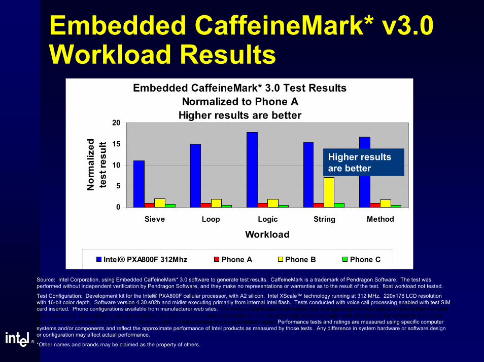
Embedded CaffeineMark* v3.0 Workload Results
Embedded CaffeineMark* 3.0 Test Results
Normalized to Phone A
Higher results are better
0
5
10
15
20
Sieve Loop Logic String Method
Workload
No
rma
lize
d
tes
t re
su
lt
Intel® PXA800F 312Mhz Phone A Phone B Phone C
Higher results
are better
Source: Intel Corporation, using Embedded CaffeineMark* 3.0 software to generate test results. CaffeineMark is a trademark of Pendragon Software. The test was
performed without independent verification by Pendragon Software, and they make no representations or warranties as to the result of the test. float workload not tested.
Test Configuration: Development kit for the Intel® PXA800F cellular processor, with A2 silicon. Intel XScale™ technology running at 312 MHz. 220x176 LCD resolution
with 16-bit color depth. Software version 4.30.s02b and midlet executing primarily from internal Intel flash. Tests conducted with voice call processing enabled with test SIM
card inserted. Phone configurations available from manufacturer web sites. For each workload test result shown, the average score of three test runs was determined and
then normalized. Normalization was accomplished by dividing the corresponding workload test result average by the average result obtained by the fastest phone tested
(e.g. Sieve avg test result of X divided by Sieve avg test for fastest phone equals normalized value). Performance tests and ratings are measured using specific computer
systems and/or components and reflect the approximate performance of Intel products as measured by those tests. Any difference in system hardware or software design
or configuration may affect actual performance.
*Other names and brands may be claimed as the property of others.

®®
Jamdat Bowling* Game Results
Source: Intel Corporation, using Jamdat Bowling* game with frame counter enabled. Received midlet from Jamdat.
Test Configuration: Development kit for the Intel® PXA800F cellular processor, with A2 silicon. Intel XScale™ technology running at 312 MHz. 220x176 LCD resolution
with 16-bit color depth. Software version 4.30.s02b and midlet executing primarily from internal Intel flash. Tests conducted with voice call processing enabled with test SIM
card inserted. Phone configurations available from manufacturer web sites. Each un-normalized test run consisted of observing frames/sec (fps), except for load time,
which was time measured by a stopwatch and inverted. The average score of three test runs was determined and then normalized. Normalization was accomplished by
dividing the corresponding workload test result average by the average result obtained by the fastest phone tested (e.g. Power Meter avg test result of X divided by Power
Meter avg test for fastest phone equals normalized value). Performance tests and ratings are measured using specific computer systems and/or components and reflect the
approximate performance of Intel products as measured by those tests. Any difference in system hardware or software design or configuration may affect actual
performance.
*Other names and brands may be claimed as the property of others.
JamDat Bowling Test Results
Normalized to Phone A
Higher results are better
0
0.5
1
1.5
2
2.5
3
3.5
1/(Load
Time)
(1/time)
Power Meter
(fps)
Aim meter
(fps)
Spin Meter
(fps)
Ball rolling
(fps)
Pins up view
(fps)
Results
table (fps)
Workload
No
rma
lize
d r
es
ult
s
Intel® PXA800F 312Mhz Phone A Phone C Phone D
Higher results
are better

®®
Agenda
Architecture/Design Challenges
GSM/GPRS overview
Chip Overview
Architectural Features
Reference Designs
Performance Results
Summary
®®
Summary
The Intel® PXA800F cellular processor integrates three key Intel technologies…
– Intel® XScale™ Microarchitecture
– Intel® Micro Signal Architecture
– Intel OnChip Flash
Integration of flash and SRAM memories with dedicated access from cores
– Provides excellent performance in both apps and comm sub-systems
– Enables low latencies, power, energy, area, noise, and cost
Chip has successfully achieved simultaneous optimization of the targeted architecture and design vectors for a GSM/GPRS phone
*Other Names and Brands may be
claimed as the property of others.