the dark side of flyback converters basso apec... · fixed or variable frequency? more power than...
TRANSCRIPT

1 • Chris Basso – APEC 2011
The Dark Side of Flyback Converters
Presented by Christophe Basso
Senior Scientist
IEEE Senior Member

2 • Chris Basso – APEC 2011
Course Agenda
The Flyback Converter
The Parasitic Elements
How These Parasitics Affect your Design?
Current-Mode is the Most Popular Scheme
Fixed or Variable Frequency?
More Power than Needed
The Frequency Response
Compensating With the TL431

3 • Chris Basso – APEC 2011
What is the Subject?
There has been numerous seminars on Flyback converters
Seminars are usually highly theoretical – link to the market?
Industrial requirements usually not covered: standby, over power…
This 3-hour seminar will shed lights on less covered topics:
Why the converter delivers more power than expected? Solutions?
Books talk about compensation with op amps, I have a TL431!
The origin of the Right-Half Plane Zero, how do I deal with it?
Quasi-resonant converters presence increases, how do they work?
In a 3-hour course, we are just scratching the surface…!

4 • Chris Basso – APEC 2011
The Flyback, a Popular Structure
The flyback converter is widely used in consumer products Ease of design, low-cost, well-known structure Poor EMI signature, bulky transformer, practical up to 150 W
flyback 40 – 180 WNotebook
flyback 3 – 5 WCharger
flyback 10 – 35 WDVD player
Set-top box
Netbook

5 • Chris Basso – APEC 2011
1
2
4
drv
7
5
drv
8
9 12
11
drvVout
VoutVout
gnd gnd
buck-boostground referenced
buck-boostinput referenced
flybackisolated ground referenced
a b c
Vin
DC
SW1
L
1 N
Vin
D
C
SW1
L
Vin
SW1
DC
An Isolated Buck-Boost
The flyback converter is derived from the buck-boost cell
The addition of a transformer brings:
Vin -k.Vin
+
• Up or down scale Vin
• Isolation
• Polarity change
• More than 1 output

6 • Chris Basso – APEC 2011
.
.
inon
p
VS
L
The current increases in the inductor in relationship to Vin and Lp
The output capacitor supplies the load on its own
inpeak valley on
p
VI I t
L
CCM
inpeak on
p
VI t
L
DCM
PIV in outV N V Reverse voltage on the diode
Simplified, no leakage
The Turn-on Event
The power switch turns on: current ramps up in Lp, D is blocked
inV
SW
pI
sec 0I
inNV outV
pL
s pN N N0 V
ont
ont
peakI
peakI
valleyI
CI
inV
pi t

7 • Chris Basso – APEC 2011
.
.
,out
DS off in in r
VV V V V
N
Reflectedvoltage
1 1out on sw
in off sw
V Nt NDT ND
V t D T D
vLp(t)
ton = DTsw toff = (1-D)Tsw
Vin
Vout/N
Apply volt-second balance
dc transfer function in CCM
Applying Volt-Second Balance, CCM
The power switch turns off: D conducts, Vout "flies" back
inV
pL
outV
outV N
pI N CI

8 • Chris Basso – APEC 2011
.
.
vLp(t)
ton = DTsw toff = (1-D)Tsw
Vout /N
Vin
DT
2out load
in p sw
V RND
V L F
,DS off inV V
Applying Volt-Second Balance, DCM
Apply volt-second balance
In DCM, when Lp is fully depleted D opens: Vout reflection is lost
dc transfer function in DCM
inV
pL0V
sec 0I CI

9 • Chris Basso – APEC 2011
24 X1PSW1RON = 10mROFF = 1Meg
3Cout470uIC = 10
V2 4 0 PULSE 0 5 0 10n 10n 3u 10u
Rload2
5
Vin100
V2
Vout6 1
X2XFMRRATIO = -0.1
Ls
VdsIIn
.
.Lp2.2m
D1
D
S
Flyback, Typical Waveforms
Below is a simple flyback converter, without parasitics
It will run open loop for simplicity, Vout 8 VNo parasitics

10 • Chris Basso – APEC 2011
Flyback, Typical Waveforms, CCM
0
400m
800m
1.20
1.60
iin in
am
pe
res
plo
t1
1
750m
850m
950m
1.05
1.15
i(lp
) in
am
pe
res
plo
t2
2
10.0
70.0
130
190
250
vds in
vo
lts
plo
t3
3
8.81
8.83
8.85
8.87
8.89
vo
ut
in v
olts
plo
t4
4
3.002m 3.006m 3.010m 3.014m 3.018mtime in seconds
0
4.00
8.00
12.0
16.0
id(d
1)
in a
mp
ere
sp
lot5
5
Iin(t)
ILp(t)
VDS(t)
Vout(t)
LI
Ipeak
VinoutV N
out inV N V
Output cap.refueling
Output capacitorsupplies the load
Diode blocks
Id(t)Ipeak / N
0
400m
800m
1.20
1.60
iin in
am
pe
res
plo
t1
1
750m
850m
950m
1.05
1.15
i(lp
) in
am
pe
res
plo
t2
2
10.0
70.0
130
190
250
vds in
vo
lts
plo
t3
3
8.81
8.83
8.85
8.87
8.89
vo
ut
in v
olts
plo
t4
4
3.002m 3.006m 3.010m 3.014m 3.018mtime in seconds
0
4.00
8.00
12.0
16.0
id(d
1)
in a
mp
ere
sp
lot5
5
Iin(t)
ILp(t)
VDS(t)
Vout(t)
LI
Ipeak
VinoutV N
out inV N V
Output cap.refueling
Output capacitorsupplies the load
Diode blocks
Id(t)Ipeak / N
CCM flyback – no parasitics
Input currentIvalley
Evalley
Epeak
Inductor current
Drain voltage
Output voltage
Diode current

11 • Chris Basso – APEC 2011
0
100m
200m
300m
400m
iin in
am
pe
res
Plo
t1
1
0
100m
200m
300m
400m
i(lp
) in
am
pe
res
Plo
t2
2
0
100
200
300
400
vds in
vo
lts
Plo
t3
3
12.632
12.636
12.640
12.644
12.648
vou
t in
vo
lts
Plo
t4
4
3.002m 3.006m 3.010m 3.014m 3.018mtime in seconds
-1.00
0
1.00
2.00
3.00
id(d
1)
in a
mp
ere
sP
lot5
5
Iin(t)
ILp(t)
VDS(t)
Vout(t)
LI
Ipeak
VinoutV Nout inV N V
DCM (core reset)
Output cap.refueling
Output capacitorsupplies the load
Diode blocks
Id(t)Ipeak / N
0
100m
200m
300m
400m
iin in
am
pe
res
Plo
t1
1
0
100m
200m
300m
400m
i(lp
) in
am
pe
res
Plo
t2
2
0
100
200
300
400
vds in
vo
lts
Plo
t3
3
12.632
12.636
12.640
12.644
12.648
vou
t in
vo
lts
Plo
t4
4
3.002m 3.006m 3.010m 3.014m 3.018mtime in seconds
-1.00
0
1.00
2.00
3.00
id(d
1)
in a
mp
ere
sP
lot5
5
Iin(t)
ILp(t)
VDS(t)
Vout(t)
LI
Ipeak
VinoutV Nout inV N V
DCM (core reset)
Output cap.refueling
Output capacitorsupplies the load
Diode blocks
Id(t)Ipeak / N
Evalley = 0
Epeak
Flyback, Typical Waveforms, DCM
Input current
Inductor current
Drain voltage
Output voltage
Diode current
DCM flyback – no parasitics

12 • Chris Basso – APEC 2011
2,
1
2pL valley p valleyE L I
2,
1
2pL peak p peakE L I
Initially stored energy
Stored energy at ton
2 2 2 2,
1 1 1
2 2 2pL accu p peak p valley p peak valleyE L I L I L I I Accumulated energy at Tsw
2 21
2out peak valley p swP I I L F CCM
DCM, Ivalley = 0
Energy Transfer in CCM and DCM
Eta, the efficiency
The primary inductance, Lp, stores and releases energy
Power (W) is energy (J) averaged over time (s):
21
2out peak p swP I L F

13 • Chris Basso – APEC 2011
Course Agenda
The Flyback Converter
The Parasitic Elements
How These Parasitics Affect your Design?
Current-Mode is the Most Popular Scheme
Fixed or Variable Frequency?
More Power than Needed
The Frequency Response
Compensating With the TL431

14 • Chris Basso – APEC 2011
84
X1PSW1RON = 10mROFF = 1Meg
3
7
Cout470uIC = 10
V2 4 0 PULSE 0 5 0 10n 10n 3u 10u
Rload2
5
Vin100
V2
Vout6
2
1
X2XFMRRATIO = -0.1
Ls
Vds
9
IIn.
.LpLp
LleakLeak
parametersLp=2.2mk=0.02Leak=Lp*k
Clump100p
D11n5819
Resr150m
rLf250m
Dbody
Considering Parasitic Elements
The transformer and the MOSFET include parasitics
With parasitics
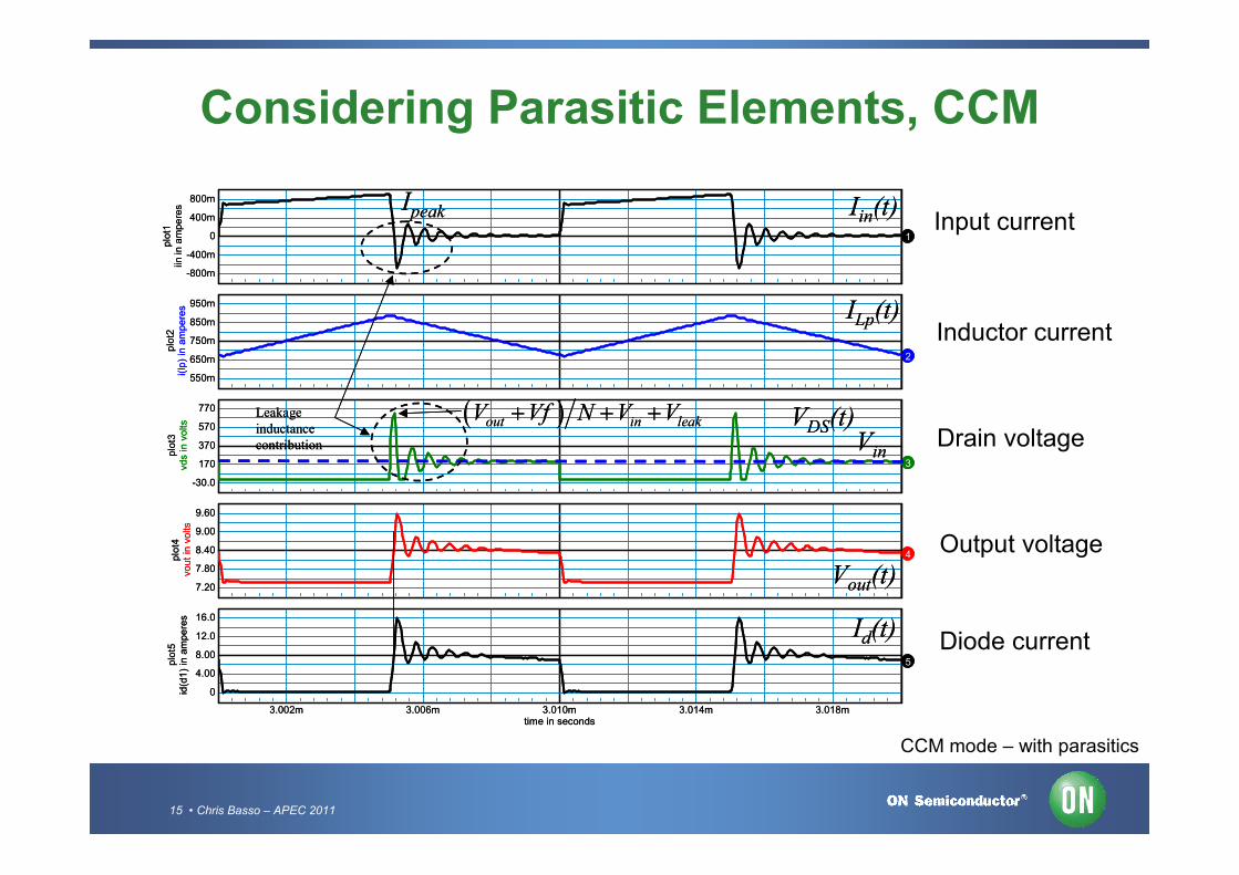
15 • Chris Basso – APEC 2011
CCM mode – with parasitics
Considering Parasitic Elements, CCM
-800m
-400m
0
400m
800m
iin in
am
pe
res
plo
t1
1
550m
650m
750m
850m
950m
i(lp
) in
am
pe
res
plo
t2
2
-30.0
170
370
570
770
vds in
vo
lts
plo
t3
3
7.20
7.80
8.40
9.00
9.60
vou
t in
vo
lts
plo
t4
4
3.002m 3.006m 3.010m 3.014m 3.018mtime in seconds
0
4.00
8.00
12.0
16.0
id(d
1)
in a
mp
ere
sp
lot5
5
Iin(t)
ILp(t)
VDS(t)
Vout(t)
Ipeak
Vin
out in leakV Vf N V V
Id(t)
Leakageinductancecontribution
Input current
Inductor current
Drain voltage
Output voltage
Diode current

16 • Chris Basso – APEC 2011
Considering Parasitic Elements, DCM
-100m
0
100m
200m
300m
iin in
am
pe
res
plo
t1
1
-100m
0
100m
200m
300m
i(lp
) in
am
pe
res
plo
t2
2
-30.0
70.0
170
270
370
vds in
vo
ltsp
lot3
3
12.2
12.4
12.6
12.8
13.0
vou
t in
vo
ltsp
lot4
4
3.002m 3.007m 3.012m 3.017m 3.022mtime in seconds
0
1.00
2.00
3.00
4.00
id(d
1)
in a
mp
ere
sp
lot5
5
Iin(t)
ILp(t)
VDS(t)
Vout(t)
Ipeak
Vin
out in leakV Vf N V V
Id(t)
Leakageinductancecontribution
DCM (core reset)
Diode blocks here
-100m
0
100m
200m
300m
iin in
am
pe
res
plo
t1
1
-100m
0
100m
200m
300m
i(lp
) in
am
pe
res
plo
t2
2
-30.0
70.0
170
270
370
vds in
vo
ltsp
lot3
3
12.2
12.4
12.6
12.8
13.0
vou
t in
vo
ltsp
lot4
4
3.002m 3.007m 3.012m 3.017m 3.022mtime in seconds
0
1.00
2.00
3.00
4.00
id(d
1)
in a
mp
ere
sp
lot5
5
Iin(t)
ILp(t)
VDS(t)
Vout(t)
Ipeak
Vin
out in leakV Vf N V V
Id(t)
Leakageinductancecontribution
DCM (core reset)
Diode blocks here
Input current
Inductor current
Drain voltage
Output voltage
Diode current
DCM mode – with parasitics

17 • Chris Basso – APEC 2011
Who Are the Stray Elements?
The study of the drain node reveals a LC network
.
..
.Lp
lleak
Coss
Lp primary inductorlleak leakage inductorCoss output capacitance
Simplified view
VbulkVbulk

18 • Chris Basso – APEC 2011
21
2OSS DSW C V
The MOSFET COSS is a Non-Linear Device
The capacitor value changes with its bias voltage
0
0
1
DOSS DS
DS
CC V
V
V
CD0 is the cap. for VDS = V0
As bias affects the capacitor value:

19 • Chris Basso – APEC 2011
As the Voltage Decreases, COSS Value Changes
The brutal discharge generates switching losses
OSSC
MOSFET
D
S
CI 0
t
C CW I t V t dt
CV
C
C
dV tI t C
dt
0 0
DSt VDS
DS DS DS DS
dV tW C V t dt C V V dV
dt
0 0D
OSS DS
DS
C VC V
V 3 2
0 0
2
3DS DW V C V
The energy lost is smaller with the non-linear variation!
At turn-off
20 • Chris Basso – APEC 2011
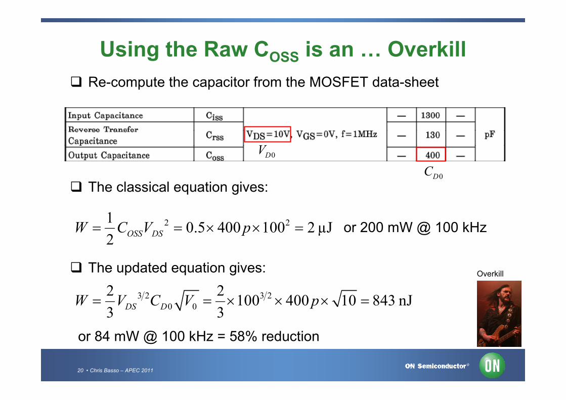
Using the Raw COSS is an … Overkill
Re-compute the capacitor from the MOSFET data-sheet
2 210.5 400 100 2 µJ
2OSS DSW C V p
The classical equation gives:
or 200 mW @ 100 kHz
The updated equation gives:
3 2 3 20 0
2 2100 400 10 843 nJ
3 3DS DW V C V p
or 84 mW @ 100 kHz = 58% reduction
0DC
0DV
Overkill
21 • Chris Basso – APEC 2011
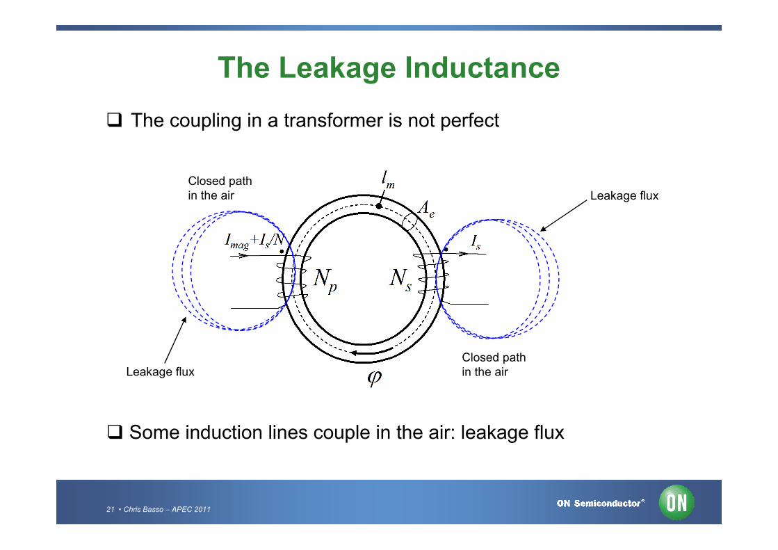
The Leakage Inductance
The coupling in a transformer is not perfect
Closed pathin the air
Closed pathin the airLeakage flux
Leakage flux
Some induction lines couple in the air: leakage flux

22 • Chris Basso – APEC 2011
An Equivalent Transformer Model
For a two-winding transformer, the model is simple:
Two leakage inductors
One magnetizing inductor
lleak1 lleak2
Lp
1:N
primary secondary
This is commonly known as the "PI" model

23 • Chris Basso – APEC 2011
The Transformer Scales the Primary Current
. .
In a perfect transformer, we have:
pIsec
pII
N
Primary Secondary
The turns ratio is usually normalized to the primary
1: N
:p sN N :p s
p p
N N
N N1: N
Divide by Np
100
25
p
s
N
N
1: 0.25
. .1 250m

24 • Chris Basso – APEC 2011
The Leakage Term also Stores Energy
At turn-on, the primary current flows in both lleak and Lp
pI t
pL
leakl
inon
p leak
VS
L l
N = 1
During the on-time, both Lp and lleak store energy
21
2leak leak pW l I
pI t
inV

25 • Chris Basso – APEC 2011
Where does the Current Flow?
At turn-off, the energy stored in Lp is dumped in the output cap.
The leakage inductor current fills up the drain lump capacitor
pL
leaklI t
p leakL lI t I t
pLI t
outV t
leaklI t
leakl
lumpC
inV
26 • Chris Basso – APEC 2011
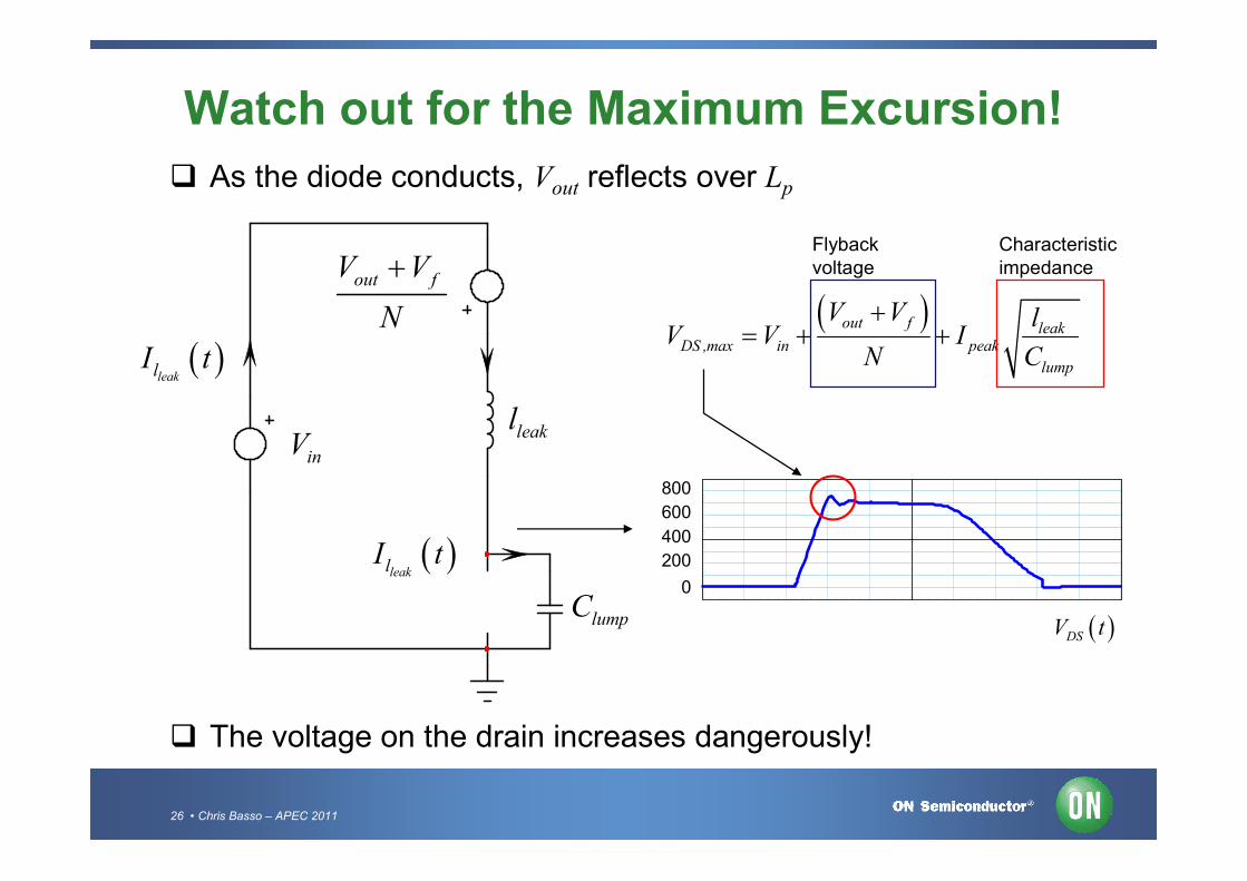
Watch out for the Maximum Excursion!
The voltage on the drain increases dangerously!
As the diode conducts, Vout reflects over Lp
leakl
lumpC
out fV V
N
out f leakDS ,max in peak
lump
V V lV V I
N C
Characteristicimpedance
inV
Flyback voltage
leaklI t
leaklI t
0
200
400
600
800
DSV t

27 • Chris Basso – APEC 2011
We Need to Clamp that Voltage
MOSFETs have a voltage limit they can fly up to: BVDSS
A clamping circuit has been installed to respect a margin
out fV V
N
clampV
clampV
pL
D D
leakl
in clampV V
600VDSSBV

28 • Chris Basso – APEC 2011
Resetting the Leakage Inductance
Because of the clamp action, a voltage appears across lleak
clampVpL
leakl
leaklI t
p leakL lI t I t
pLI t
leaklI t
outV t
leak
clamp out f
l
leak
V V VS
l
This voltage forces a reset of the leakage inductance
leakl clamp out fV V V V
leaklV
29 • Chris Basso – APEC 2011
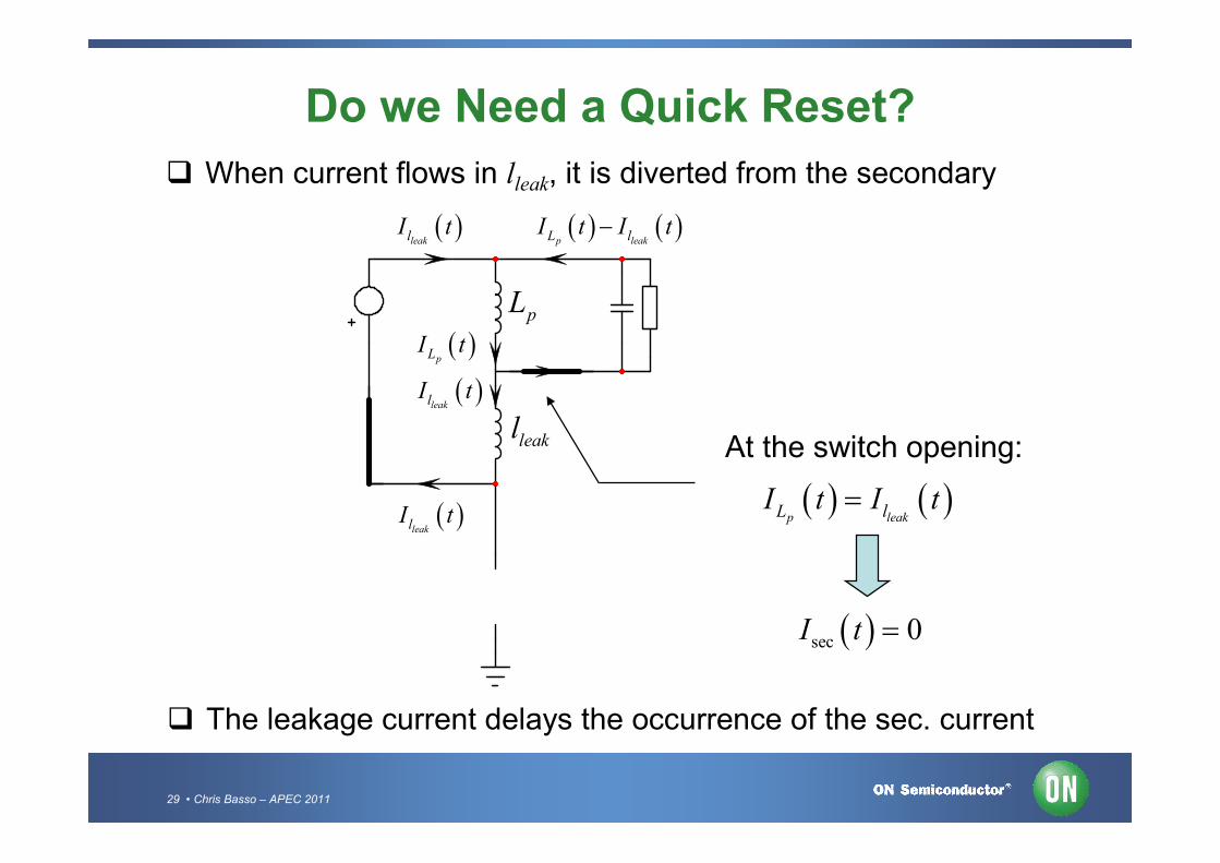
Do we Need a Quick Reset?
When current flows in lleak, it is diverted from the secondary
leaklI t
p leakL lI t I t
pLI t
leaklI t
leaklI t
The leakage current delays the occurrence of the sec. current
At the switch opening:
p leakL lI t I t
sec 0I t
pL
leakl

30 • Chris Basso – APEC 2011
lleak Delays the Secondary Current
The leakage inductor reduces the peak secondary current
I t
t
ont t offt t
peakI
valleyI
,p leakL lI I
leaklI
secI
Primary and secondary currents.
secI t
pI t
The "stolen" energy is dissipated as heat in the clamping network Less energy is transmitted to the secondary side
pI
31 • Chris Basso – APEC 2011
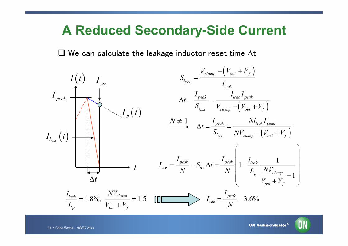
A Reduced Secondary-Side Current
We can calculate the leakage inductor reset time t
sec sec
11
1
peak peak leak
clampp
out f
I I lI S t
NVN N L
V V
leak
peak leak peak
l clamp out f
I l It
S V V V
leak
peak leak peak
l clamp out f
I Nl It
S NV V V
N 1
I t
t
peakI
secI
pI t
t
leak
clamp out f
l
leak
V V VS
l
leaklI t
1.8%, 1.5clampleak
p out f
NVl
L V V
sec 3.6%
peakII
N
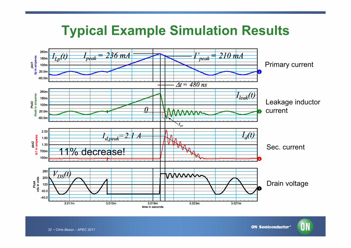
32 • Chris Basso – APEC 2011
-60.0m
20.0m
100m
180m
260m
ilp in
am
pe
res
plo
t1
2
-60.0m
20.0m
100m
180m
260m
ille
ak
in a
mp
ere
sP
lot3
3
100m
700m
1.30
1.90
2.50
id1
in a
mp
ere
sp
lot2
4
3.011m 3.015m 3.019m 3.023m 3.027mtime in seconds
-40.0
40.0
120
200
280
vds in
vo
lts
Plo
t4
1
ILp(t)
Id(t)
VDS(t)
Ileak(t)
Ipeak = 236 mA I’peak = 210 mA
0
Id,peak=2.1 A
trr
t = 480 ns-60.0m
20.0m
100m
180m
260m
ilp in
am
pe
res
plo
t1
2
-60.0m
20.0m
100m
180m
260m
ille
ak
in a
mp
ere
sP
lot3
3
100m
700m
1.30
1.90
2.50
id1
in a
mp
ere
sp
lot2
4
3.011m 3.015m 3.019m 3.023m 3.027mtime in seconds
-40.0
40.0
120
200
280
vds in
vo
lts
Plo
t4
1
ILp(t)
Id(t)
VDS(t)
Ileak(t)
Ipeak = 236 mA I’peak = 210 mA
0
Id,peak=2.1 A
trr
t = 480 ns
Typical Example Simulation Results
Primary current
Leakage inductorcurrent
Sec. current
Drain voltage
11% decrease!

33 • Chris Basso – APEC 2011
..
A Ringing Appears as the Diode Blocks
0leaklI t
in clamp rV V V
rV
leakl
As the clamp diode blocks, the drain returns toVin
out f
in
V VV
N
An oscillationtakes place
1
2 leak lump
fl C
outV
lumpC
lleak is resett
1: N

34 • Chris Basso – APEC 2011
The Primary Inductor also Rings in DCM
When Lp is reset, the capacitor voltage returns to Vin
..
0 V
leakl
lumpC in rV V
An oscillationtakes place
1
2 p leak lump
fL l C
Lp is reset
Vin
Vin
1: N

35 • Chris Basso – APEC 2011
Course Agenda
The Flyback Converter
The Parasitic Elements
How These Parasitics Affect your Design?
Current-Mode is the Most Popular Scheme
Fixed or Variable Frequency?
More Power than Needed
The Frequency Response
Compensating With the TL431

36 • Chris Basso – APEC 2011
The leakage inductor induces a large spike at turn-off This voltage excursion must be kept under control
How these Parasitics Affect your Design?
BVDSS
clampV 15%
V
t
The lump capacitor on the drain brings switching losses Is there a way to switch on again when discharged?
Asynchronous switchingFixed frequency
Synchronous switchingVariable frequency
DS inV V
DS inV V DSV t DSV t
VinVin
Vin

37 • Chris Basso – APEC 2011
600 0.85 510 VDSS DBV k
115 Vclamp DSS D os inV BV k V V
A vertical MOSFET features a buried parasitic NPN transistor
The collector-base junction of this transistor forms the body-diode
This « diode » can accept to avalanche in certain conditions
Do NOT use this diode as a Transient Voltage Suppressor
Adopt a safety coefficient kD when chosing the maximum VDS(t)
15% derating is usually selected
kD = 0.85
Take Vos around 15 – 20 VRCD clamp design entry
Protecting the Power MOSFET
gate
drain
source

38 • Chris Basso – APEC 2011
BVDSS = 600 V
VDS(t)
Vr Vin
Vclamp
Vos
Safety margin
100 V /div
Inclusion of a Safety Margin
The voltage on the drain swings up to Vclamp
Capture this waveform in worst-case conditions
nominal
max
max
out
out
in
V
I
V
Test at start-up
and in short-circuit

39 • Chris Basso – APEC 2011
VDS(t)
Vos = 14 V
The clamp diode forward transit time delays the clamping action
The Clamp Circuit Overshoots
This spike can be lethal to the power MOSFET
40 • Chris Basso – APEC 2011
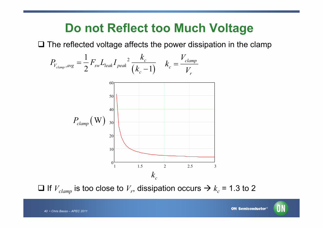
The reflected voltage affects the power dissipation in the clamp
Do not Reflect too Much Voltage
2
,
1
2 1clamp
cV avg sw leak peak
c
kP F L I
k
clamp
c
r
Vk
V
1 1.5 2 2.5 30
10
20
30
40
50
60
ck
WclampP
If Vclamp is too close to Vr, dissipation occurs kc = 1.3 to 2

41 • Chris Basso – APEC 2011
c out f
clamp
k V VN
V
The turns ratio affects the reflected voltage…
PIV in outV N V
Compute the Transformer Turns Ratio
But also the Peak Inverse Voltage of the secondary diode
Choose a 100%derating factor
PIV 100V
BV 200V
PIV
ringing
If
Then
Always check the margins are not violated in any operating modes
Vf
dV t
out f
clamp c
V VV k
N

42 • Chris Basso – APEC 2011
2
2out f
clamp clamp
clp
sw leak peak
V VV V
NR
F l I
clamp
clp
clp sw
VC
R F V
Select the Clamp Passive Elements The clamp resistor depends on the maximum peak current
600 V
550 V
600 V
550 V
clpC clpR
D
Watch for the peak current overshoot in fault!
,max ,max
,max
sense in
peak prop
sense p
V VI t
R L
Worst-case value
43 • Chris Basso – APEC 2011
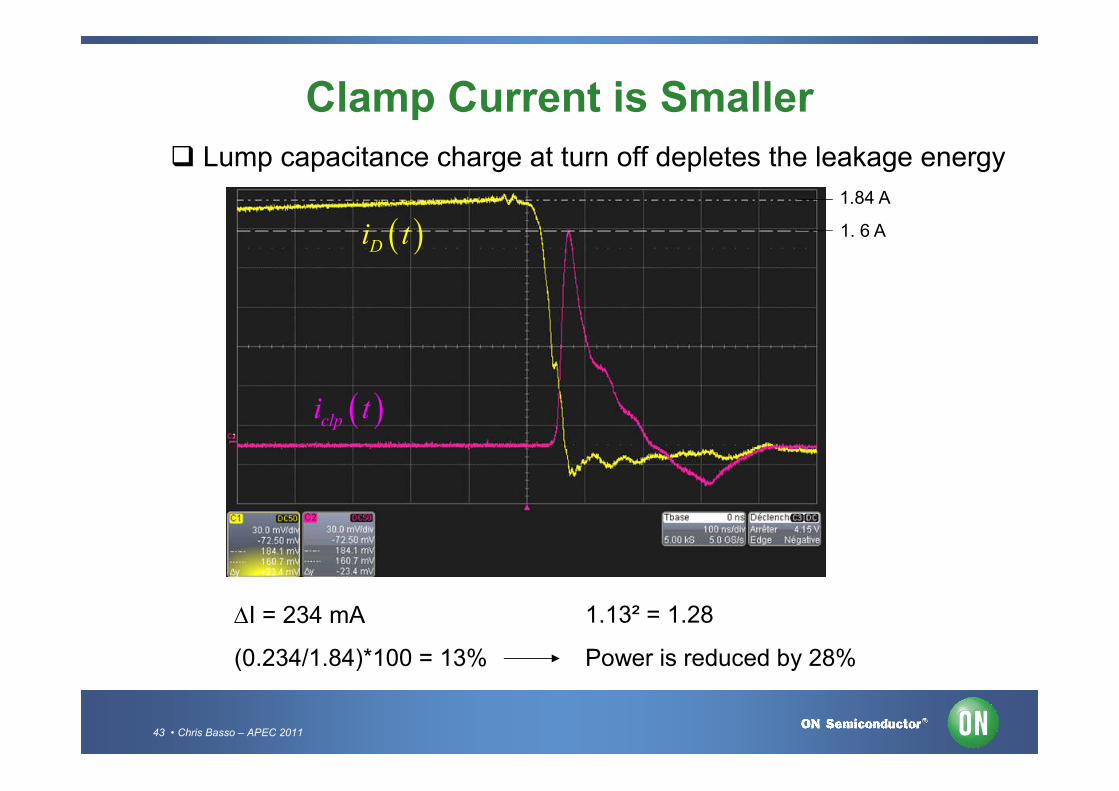
Clamp Current is Smaller
Lump capacitance charge at turn off depletes the leakage energy
Di t
clpi t
1.84 A
1. 6 A
I = 234 mA
(0.234/1.84)*100 = 13%
1.13² = 1.28
Power is reduced by 28%

44 • Chris Basso – APEC 2011
It can also forward-bias the MOSFET body diode Damp it!
VDS(t)
The Leakage Inductor Rings
This ringing can be of high frequency and is radiated-EMI rich
.
.
dampR
D
clpC
clpR

45 • Chris Basso – APEC 2011
0 1leak
damp
lQ
R
0@
leakl dampZ f R
V
Without Rdamp
With Rdamp
Similarovershoot
VDS(t) VDS(t)a b
V
Without Rdamp
With Rdamp
Similarovershoot
VDS(t) VDS(t)a b
Fighting Parasitic Ringing – part I
The installed resistor reduces the ringing on the drain

46 • Chris Basso – APEC 2011
Fighting Parasitic Ringing – part II
.
.
If the series resistor is not enough, install a damper
1. Measure the ringing: f0
2. Evaluate leakage impedance at f0
3. Make
4. Try
5. Tweak for power dissipation0
1
2dampC
f R
leakdamp lR Z
02leakl leakZ l f
Ray Ridley – Snubber design procedure
dampR
dampC

47 • Chris Basso – APEC 2011
3.0325m 3.0335m 3.0345m 3.0355m 3.0365mtime in seconds
40.0
160
280
400
520
vdra
in in
vo
ltsp
lot1
1
3.042m 3.046m 3.050m 3.054m 3.058mtime in seconds
10.0
130
250
370
490
vdra
in in
vo
ltsP
lot5
2
3.042m 3.046m 3.050m 3.054m 3.058mtime in seconds
10.0
130
250
370
490
vdra
in#a
in v
olts
Plo
t4
3
3.042m 3.046m 3.050m 3.054m 3.058mtime in seconds
10.0
130
250
370
490
vdra
in#a
in v
olts
Plo
t3
3
No damper – zoom
Vpeak = 510 V
Can forward biasthe body diode No damper
VDS(t)
VDS(t)
VDS(t)
VDS(t)
Rdamp = 290 – Cdamp = 220 pF
Rdamp = 290 – Cdamp = 50 pF
Vpeak = 452 V
Vpeak = 494 V
a
b
c
Fleak = 2.08 MHz
Effects brought by clamping action

48 • Chris Basso – APEC 2011
VDS(t)
VDS(t)
No ringing!
Recovery losses
V = 37 V
Id(t)
VDS(t)
VDS(t)
No ringing!
Recovery losses
V = 37 V
Id(t)
Can a simple 1N4007 be used in a RCD clamping network?
The answer is yes for low power applications (below 20 W)
The long recovery time naturally damps the leakage inductor
What Diode to Select for the Clamp?
A fast diode is a must: MUR160 is good fit

49 • Chris Basso – APEC 2011
0 1 2 340
60
80
100
120
140
)Vclamp (V)
Ipeak (A)0 1 2 340
60
80
100
120
140
)Vclamp (V)
Ipeak (A)
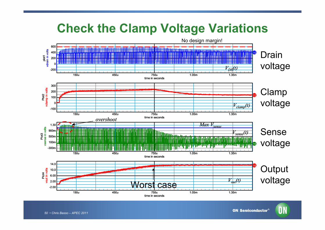
Watch-out for clamp voltage variations, at start-up or in short-circuit
The main problem comes from the propagation delay!
Be Sure the Clamp Level does not Runaway
50 • Chris Basso – APEC 2011
150u 450u 750u 1.05m 1.35mtime in seconds
-200
0
200
400
600vd
rain
in v
olts
plo
t1
10
150u 450u 750u 1.05m 1.35mtime in seconds
-100
0
100
200
300
vcla
mp
in v
olts
Plo
t2 12
150u 450u 750u 1.05m 1.35mtime in seconds
-300m
100m
500m
900m
1.30
vse
nse
in v
olts
Plo
t3
15
150u 450u 750u 1.05m 1.35mtime in seconds
-2.00
2.00
6.00
10.0
14.0
vou
t in
vo
lts
Plo
t4
16
VDS(t)
Vclamp(t)
Vsense(t)
Vout(t)
overshootMax Vsense
150u 450u 750u 1.05m 1.35mtime in seconds
-200
0
200
400
600vd
rain
in v
olts
plo
t1
10
150u 450u 750u 1.05m 1.35mtime in seconds
-100
0
100
200
300
vcla
mp
in v
olts
Plo
t2 12
150u 450u 750u 1.05m 1.35mtime in seconds
-300m
100m
500m
900m
1.30
vse
nse
in v
olts
Plo
t3
15
150u 450u 750u 1.05m 1.35mtime in seconds
-2.00
2.00
6.00
10.0
14.0
vou
t in
vo
lts
Plo
t4
16
VDS(t)
Vclamp(t)
Vsense(t)
Vout(t)
overshootMax Vsense
No design margin!
Check the Clamp Voltage Variations
Drain voltage
Clamp voltage
Sense voltage
Output voltageWorst case

51 • Chris Basso – APEC 2011
Vout
Dclp
Vbulk
TVS
VDS(t)
Id(t)
200t ns
VDS(t)
Id(t)
200t ns
21
2z
TVS sw leak peak
out f
z
VP F l I
V VV
N
The TVS improves the efficiency in standby but degrades EMI
It costs around 5 cents…
A Zener or TVS to Hard Clamp the Voltage
TVS do not suffer from voltage runaways in fault conditions

52 • Chris Basso – APEC 2011
Course Agenda
The Flyback Converter
The Parasitic Elements
How These Parasitics Affect your Design?
Current-Mode is the Most Popular Scheme
Fixed or Variable Frequency?
More Power than Needed
The Frequency Response
Compensating With the TL431

53 • Chris Basso – APEC 2011
What Control Scheme?
Two control scheme coexist, current-mode and voltage-mode
Voltage-mode?
Current-mode?
Operating waveforms are identical
Voltage-mode?
Current-mode?
Ac -transfer functions differ

54 • Chris Basso – APEC 2011
S
R
Q
Q
+
-
.
.
+
-
Voltage-Mode Control Voltage mode uses a ramp to generate the duty-ratio
The error voltage directly adjusts the duty-ratio
senseR
maxV
outV
FB
ddv
bulkV
D t
errV t
sawV t
D t
errV

55 • Chris Basso – APEC 2011
Voltage-Mode Control
PROsPROs
Does not need the inductor current information
Can go to very small duty-ratio
CCM operation without sub-harmonic instabilities
No need for slope compensation, current limit unaffected
CONsCONs
No inherent input line feedforward (weak audio susceptibility)
Cannot use small bulk capacitor, bad ripple rejection
2nd-order system in CCM: mode transition can be a problem
Limited integrated circuit offer

56 • Chris Basso – APEC 2011
Peak-Current-Mode Control
S
R
Q
Q
+
-
.
.
senseR
maxV
outV
FB
ddv
errV
bulkV
Current mode uses the inductor current information as a ramp The error voltage adjusts the inductor peak current
The duty-ratio is indirectly controlled
D t
LI t errV t
LI t

57 • Chris Basso – APEC 2011
Peak-Current-Mode Control
PROsPROs
Inherent pulse-by-pulse current limitation
Natural input line rejection
Mode transition DCM to CCM is easy
Converter remains a 1st-order system at low frequency
Widest offer on the market: a really popular technique!
CONsCONs
Leading Edge Blanking limits the minimum duty-ratio
Requires slope compensation against sub-harmonic oscillations
Additionnal ramp affects the available maximum peak current
Current sense can sometimes be a problem (floating sense)

58 • Chris Basso – APEC 2011
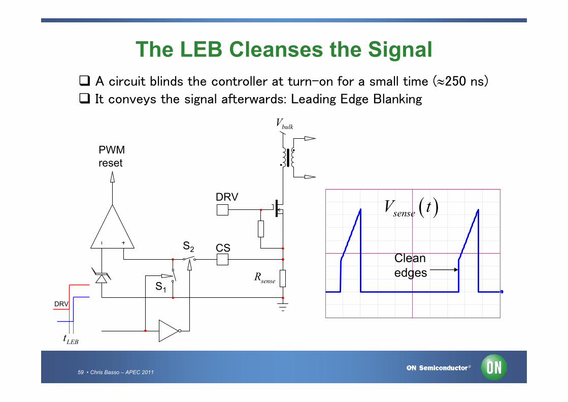
A Dirty Inductor Current Signal
The inductor current is sensed with a resistor, a transformer…
This information is affected by parasitics: false tripping possible!
3.122m 3.126m 3.131m 3.135m 3.139m
-100m
100m
300m
500m
700m
1
senseV t
Can potentially false trip the controller
59 • Chris Basso – APEC 2011
The LEB Cleanses the Signal
A circuit blinds the controller at turn-on for a small time (250 ns)
It conveys the signal afterwards: Leading Edge Blanking
2
2
senseV t
Cleanedges
senseR
CS
DRV
S1
S2
PWMreset
bulkV
DRV
LEBt
..
60 • Chris Basso – APEC 2011
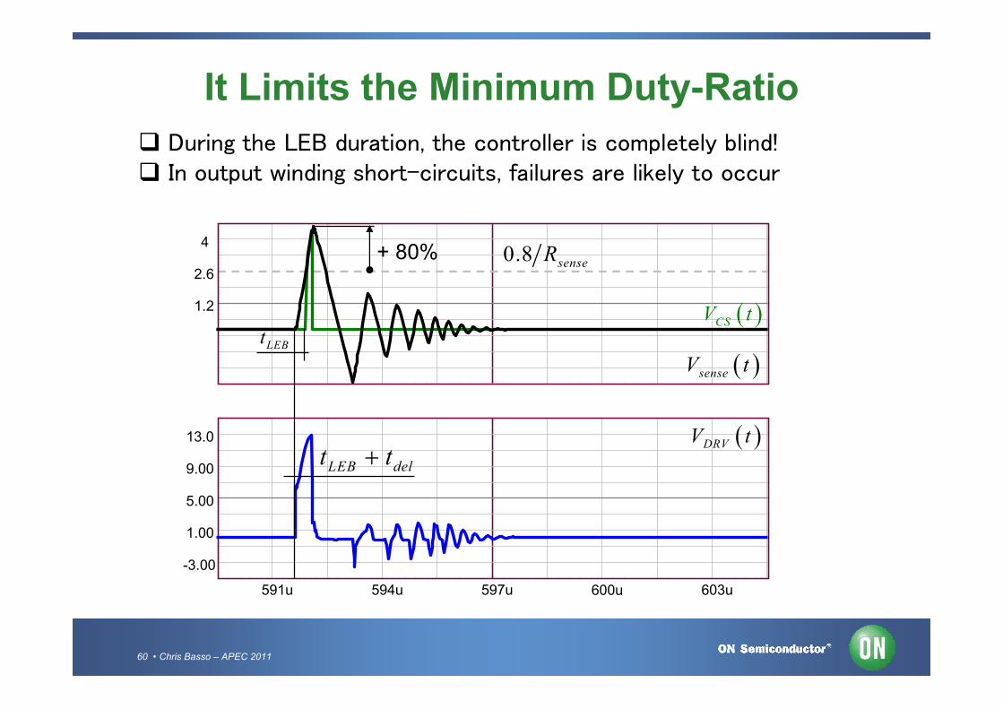
It Limits the Minimum Duty-Ratio
During the LEB duration, the controller is completely blind! In output winding short-circuits, failures are likely to occur
1.2
2.6
4
591u 594u 597u 600u 603u
-3.00
1.00
5.00
9.00
13.0
0.8 senseR
LEBt
+ 80%
LEB delt t DRVV t
senseV t
CSV t
61 • Chris Basso – APEC 2011
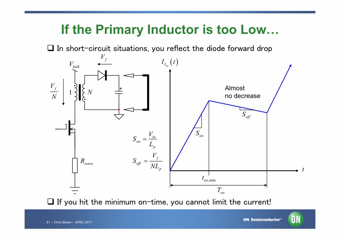
If the Primary Inductor is too Low…
In short-circuit situations, you reflect the diode forward drop
.
.
bulkV
1 N
fV
fV
N
pLI t
tsenseR
inon
p
f
off
p
VS
L
VS
NL
onS
offS
swT
,minont
Almostno decrease
If you hit the minimum on-time, you cannot limit the current!

62 • Chris Basso – APEC 2011
1.00
3.00
5.00
7.00
9.00
ipri
m in
am
pe
res
Plo
t1
7
35.0u 70.0u 105u 140u 175utime in seconds
0
400m
800m
1.20
1.60
vse
nse
in
volts
Plo
t2
8
ILp(t)
Vsense(t)
Demagnetizationtoo weak
1 V
Maximum theoreticalpeak value, 5 A
The current climbs-up to 9 A!!
1.00
3.00
5.00
7.00
9.00
ipri
m in
am
pe
res
Plo
t1
7
35.0u 70.0u 105u 140u 175utime in seconds
0
400m
800m
1.20
1.60
vse
nse
in
volts
Plo
t2
8
ILp(t)
Vsense(t)
Demagnetizationtoo weak
1 V
Maximum theoreticalpeak value, 5 A
The current climbs-up to 9 A!!
Chris Bassofirst design…
The Primary Current Runs out of Control
The current current climbs cycle by cycle until smoke appears!
Minimum ton
ok

63 • Chris Basso – APEC 2011
Sub-Harmonic Oscillations Ac analysis shows a first-order system at fc << Fsw/2
No LC peaking anymore as in CCM voltage mode
But a subharmonic peaking at Fsw/2 now appears
-15.0
-5.00
5.00
15.0
25.0
1 10 100 1k 10k 100k
-180
-90.0
0
90.0
180
H s
H s Flyback power stage in CCM

64 • Chris Basso – APEC 2011
IL
tdTsw d’Tsw
Tsw
IL(0)
IL(Tsw)
S1S2
t
ab
IL(0) IL(Tsw)err
i
V
R
IL(Tsw)IL(0)
Ipeak
IL
tdTsw d’Tsw
Tsw
IL(0)
IL(Tsw)
S1S2
t
ab
IL(0) IL(Tsw)err
i
V
R
IL(Tsw)IL(0)
IL
tdTsw d’Tsw
Tsw
IL(0)
IL(Tsw)
S1S2
t
ab
IL(0) IL(Tsw)err
i
V
R
IL(Tsw)IL(0)
Ipeak
( ) (0)'
n
L sw L
dI nT I
d
1peakI a S t
2peakb I S t
1 2
peak peakI a I b
S S
Solvingt
1 2
( )(0) L swL I TI
S S
2
1 '
S d
S d
Instability Depends on Duty-Ratio The condition for instability is: CCM operation + duty-ratio > 50%

65 • Chris Basso – APEC 2011
clock
Ipeak
IL
Perturbation has gone…
IL(0)
IL(0)
t
clock
Ipeak
IL
Perturbation has gone…
IL(0)
IL(0)
t
IL(0)
clock
Ipeak
Duty clamp
IL
IL(0)
t
IL(0)
clock
Ipeak
Duty clamp
IL
IL(0)
t
clock
Ipeak
Duty clamp
IL
IL(0)
t
Duty-ratio < 50%
Duty-ratio > 50%
Asymptotically stable
Asymptotically unstable
( ) (0)'
n
L sw L
dI nT I
d
Instability Depends on Duty-Ratio With a duty-ratio below 50%, perturbation naturally dies out …

66 • Chris Basso – APEC 2011
IL
tdTsw d’Tsw
Tsw
IL(0)
IL(Tsw)
S1
S2
t
IL(0)
Sa
cb
IL(Tsw)
err
i
V
R
IL
tdTsw d’Tsw
Tsw
IL(0)
IL(Tsw)
S1
S2
t
IL(0)
Sa
cb
IL(Tsw)
err
i
V
R
2
2
1
( ) (0) (0)'
n
a
n
L sw L La
S
SI nT I I a
Sd
d S
Must staybelow 1
2
2
1
1
0
a
a
S
S
S
S
250%aS S
Up tod = 100%
The Cure is in the Ramp Injecting a ramp on the feedback signal, damping is obtained

67 • Chris Basso – APEC 2011
A Model to Simulate a Flyback Converter A SPICE model can predict subharmonic instabilities
1
D1Ambr20200ctp
23
4
LpLp
5DC
vout6
vout
X2xXFMRRATIO = -N
Vin100AC = 0
8
R1014.4m
C56600u
vca
c
PW
M s
witc
h C
Mp
du
ty-c
ycle
X9PWMCML = LpFs = FswRi = RiSe = Se
Rload4
parameters
Vout=19Soff=(Vout/(N*Lp))*Ri
N=250mFsw=65kLp=350uRi=250mA=0.5Se=A*Soff
10
R166k
R210k
9
12
X3AMPSIMP
V22.5
13
LoL1kH
15
CoL1kF
AC = 1Vstim
err
B1Voltage
V(err)/3 > 1 ?1 : V(err)/3
19.7V 19.0V
0V
441mV
-79.0V100V
19.0V
774mV
2.50V
2.50V2.32V2.32V
2.32V
0V

68 • Chris Basso – APEC 2011
Simulation Results of the CCM Flyback As ramp is injected, the double-pole Q is damped
Injecting more ramp turns the converter into voltage-mode
-24.0
-12.0
0
12.0
24.0
1 10 100 1k 10k 100k
-180
-90.0
0
90.0
180
No ramp
H s
H s
250%aS S
No ramp
250%aS S
69 • Chris Basso – APEC 2011
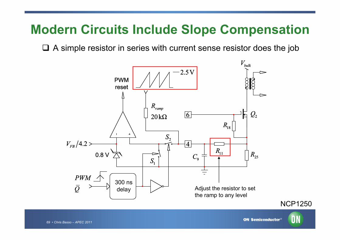
Modern Circuits Include Slope Compensation
A simple resistor in series with current sense resistor does the job
6
411R
9C
bulkV
18R
2Q
25R
20 kΩ
rampR
300 nsdelay
PWM
Q
4.2FBV
PWMreset
2.5V
0.8 V
1S
2S
..
6
411R
9C
bulkV
18R
2Q
25R
20 kΩ
rampR
300 nsdelay
PWM
Q
4.2FBV
PWMreset
2.5V
0.8 V
1S
2S
..
NCP1250
Adjust the resistor to set the ramp to any level

70 • Chris Basso – APEC 2011
Course Agenda
The Flyback Converter
The Parasitic Elements
How These Parasitics Affect your Design?
Current-Mode is the Most Popular Scheme
Fixed or Variable Frequency?
More Power than Needed
The Frequency Response
Compensating With the TL431

71 • Chris Basso – APEC 2011
Modulation Strategies
on
off
off
on
LeadingLeading edge modulation
TrailingTrailing edge modulation
Clock
Clock
off
feedback
feedback
The most popular modulation strategy is trailing-edge
Leading-edge modulation often appears in post-regulators
vGS(t)
vGS(t)
72 • Chris Basso – APEC 2011
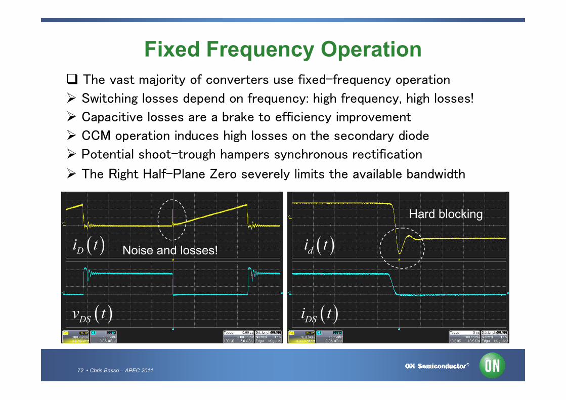
Fixed Frequency Operation
The vast majority of converters use fixed-frequency operation
Switching losses depend on frequency: high frequency, high losses!
Capacitive losses are a brake to efficiency improvement
CCM operation induces high losses on the secondary diode
Potential shoot-trough hampers synchronous rectification
The Right Half-Plane Zero severely limits the available bandwidth
DSv t
Di t di t
DSi t
Hard blocking
Noise and losses!

73 • Chris Basso – APEC 2011
In a CCM flyback, Iout is delivered during the off-time:
Tsw
D0Tsw
id(t)
t
IL(t)
in
p
V
L
Id0
Tsw
D1Tsw
id(t)
t
IL(t)
d
IL1
Id1
IL0
If D brutally increases, D' reduces and Iout drops! What matters is the inductor current slew-rate
Ldv t
dt
in
p
V
L
The Right-Half-Plane Zero

74 • Chris Basso – APEC 2011
Processing the Output Power Demand If iL(t) can rapidly change, Iout increases when D goes up
100u 300u 500u 700u 900u
d(t) vout(t)
iL(t)
iout(t)
200 µs
d = 58.3%
d = 59%

75 • Chris Basso – APEC 2011
If iL(t) is limited because of a big Lp, Iout drops when D increases
2
100u 300u 500u 700u 900u
d(t)
d = 59%
d = 58.3%
vout(t)
iL(t)
iout(t)
10 µs
Vout drops!
Iout drops!
Failing to Increase the Current in Time

76 • Chris Basso – APEC 2011
Small-signal equations can help us to formalize it
2
2
2
'loadz
R D
N DL
The negative signindicates a positive root!
1 2
0 2
0 0
1 1ˆ
ˆ1
z zout
s s
v sG
d s s s
Q
Voltagemode
Currentmode
Voltage mode or current mode, the RHPZ remains the same
1 2 3
0
1 1 1ˆ
ˆ
z z zout
c
s s s
v sG
v s D s
The RHPZ is a Positive Root
77 • Chris Basso – APEC 2011
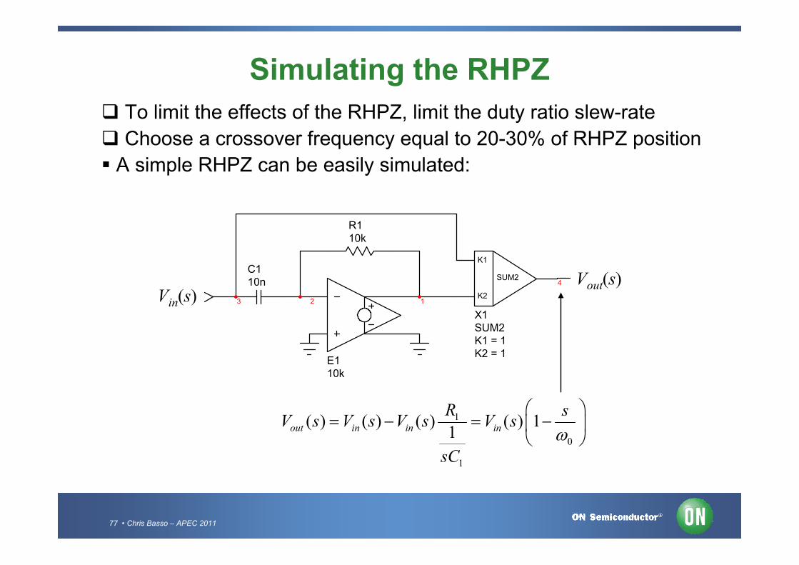
To limit the effects of the RHPZ, limit the duty ratio slew-rate
Choose a crossover frequency equal to 20-30% of RHPZ position
A simple RHPZ can be easily simulated:
12
E110k
R110k
3
C110n
SUM2
K1
K2
4
X1SUM2K1 = 1K2 = 1
Vin
1
0
1
( ) ( ) ( ) ( ) 11out in in in
R sV s V s V s V s
sC
Vout(s)Vin(s)
Simulating the RHPZ

78 • Chris Basso – APEC 2011
With a RHPZ we have a boost in gain but a lag in phase!
0
( ) 1s
G s
LHPZ
RHPZ
0
( ) 1s
G s
-40.0
-20.0
0
20.0
40.0
1 10 100 1k 10k 100k 1Meg
frequency in hertz
-180
-90.0
0
90.0
180
|Vout(s)|
argVout(s)
-90°
+1
A Zero Producing a Phase Lag

79 • Chris Basso – APEC 2011
A RHPZ also exists in DCM boost, buck-boost converters…
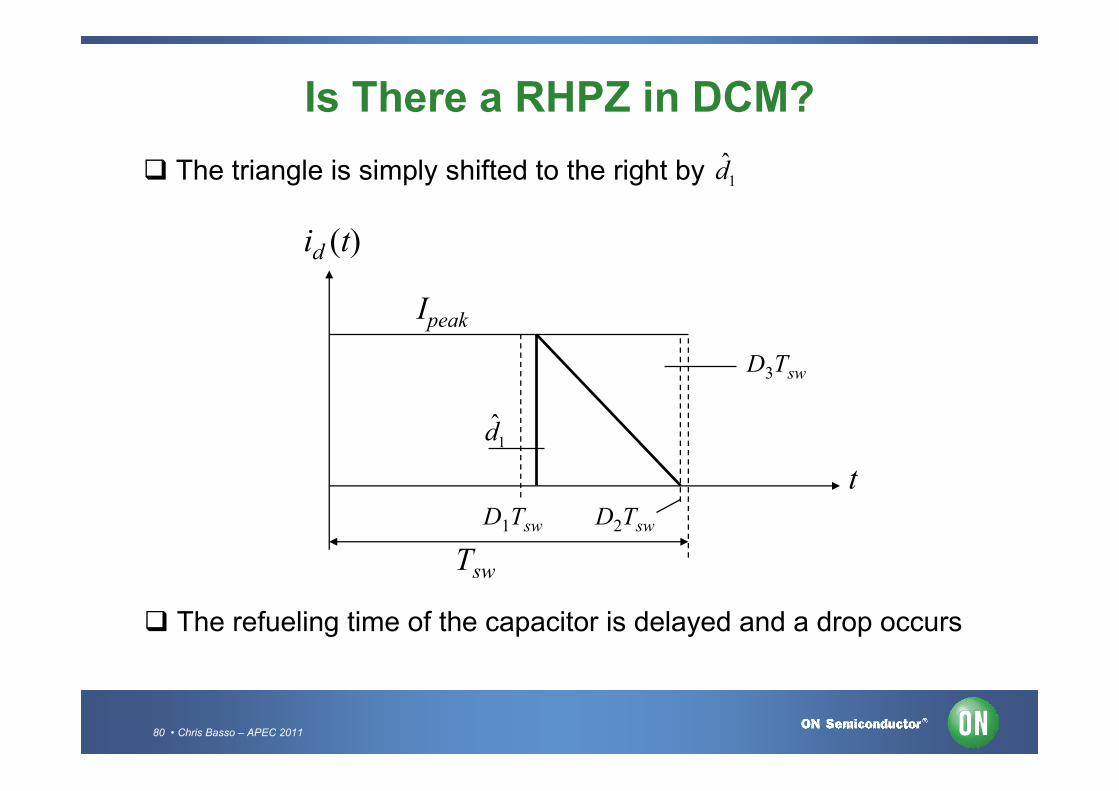
When D1 increases, [D1, D2] stays constant but D3 shrinks
Is There a RHPZ in DCM?
Tsw
D1Tsw
id (t)
t
D2Tsw
D3Tsw
Ipeak
80 • Chris Basso – APEC 2011
Tsw
D1Tsw
tD2Tsw
D3Tsw
1d
The triangle is simply shifted to the right by 1d
The refueling time of the capacitor is delayed and a drop occurs
Is There a RHPZ in DCM?
id (t)
Ipeak
81 • Chris Basso – APEC 2011
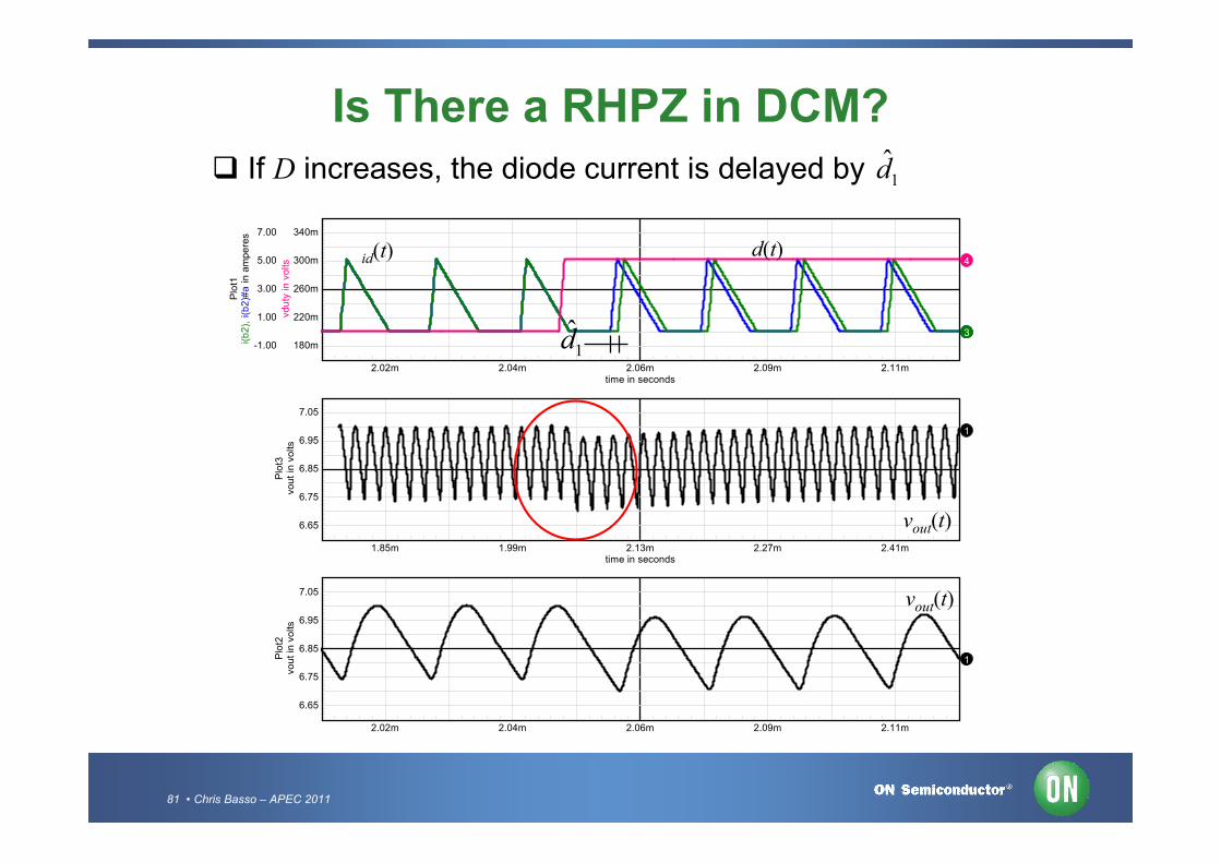
If D increases, the diode current is delayed by
2.02m 2.04m 2.06m 2.09m 2.11mtime in seconds
180m
220m
260m
300m
340m
vdu
ty in v
olts
-1.00
1.00
3.00
5.00
7.00i(b
2),
i(b
2)#
a in a
mpe
res
Plo
t1
23
4
1.85m 1.99m 2.13m 2.27m 2.41mtime in seconds
6.65
6.75
6.85
6.95
7.05
vou
t in
volts
Plo
t3
1
2.02m 2.04m 2.06m 2.09m 2.11mtime in seconds
6.65
6.75
6.85
6.95
7.05
vou
t in
volts
Plo
t2
1
d(t)id(t)
vout(t)
vout(t)
1d
1d
Is There a RHPZ in DCM?

82 • Chris Basso – APEC 2011
Averaged models can predict the DCM RHPZ
Vout
16
R11150
C51m
R10150m
3
Vin10V
11
L175u
5
R150k
R310k
6
8
X2AMPSIMP
V22.5
Verr
1
LoL1kH
10
CoL1kF
V1xAC = 1
vout
vout
dac
PW
M s
witc
h V
Mp
X3PWMVML = 75uFs = 100k
15.0V
15.0V
10.0V
10.0V
2.50V
278mV278mV
0V
1
1
2
2
1 1ˆ
ˆ 1 1
z zoutd
p p
s s s sv sH
d s s s s s
1
1z
out ESR
sC R
2 2
loadz
Rs
M L
1
2 1 1
1p
out ESR
Ms
M C R
2
21 1
2p sw
Ms F
D
2 1
2 1out
d
V MH
D M
MerciVatché!
A Large-Signal Model is Available

83 • Chris Basso – APEC 2011
Averaged models can predict the DCM RHPZ
11.06zf kHz
2141zf kHz
14.2pf Hz
28.75dH dB
247.1pf kHz
28.6 dB
-45°
fp1
4.2 Hz 1 kHz 47 kHz 141 kHz
The Model Predicts it!
1 10 100 10k 100k 1Meg
-40.0
-20.0
0
20.0
40.0
-180
-90.0
0
90.0
180
8
7
fz2
fp2
fz1

84 • Chris Basso – APEC 2011
Going to Variable Frequency
More converters are using variable-frequency operation
This is known as Quasi-Square Wave Resonant mode: QR
Valley switching ensures extremely low capacitive losses
DCM operation saves losses on the secondary diode
Easier synchronous rectification
The Right Half-Plane Zero is pushed to high frequencies
DSv t
Di t di t
DSv t
Smooth signals
Less noise
Low CV² losses

85 • Chris Basso – APEC 2011
What is the Principle of Operation?
The drain-source signal is made of peaks and valleys
A valley presence means:
The drain is at a minimum level, capacitors are naturally discharged
The converter is operating in the discontinuous conduction mode
2.061m 2.064m 2.066m 2.069m 2.071m
0
120
240
360
480
DSv tDTtoffton
Vin
valley
V

86 • Chris Basso – APEC 2011
A QR Circuit Does not Need a Clock The system is a self-oscillating current-mode converter
S
R
Q
Q
+
-
.
.+
-
.
GFB Rsense
Vout
Cout
Resr
Rload
Rpullup
Np:Ns
Vdd
Vbulk
FB
Lp
CTR
65 mV
Demagdetector
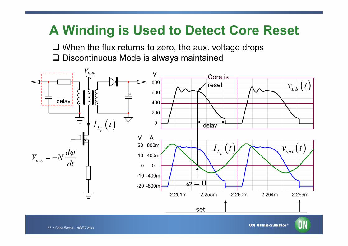
87 • Chris Basso – APEC 2011
A Winding is Used to Detect Core Reset
0
200
400
600
800
2.251m 2.255m 2.260m 2.264m 2.269m
-800m
-400m
0
400m
800m
-20
-10
0
10
20
V A
V
DSv t
pLI t
. .
.
pLI t
bulkV
aux
dV N
dt
0
Core is reset
delay
delay
auxv t
When the flux returns to zero, the aux. voltage drops Discontinuous Mode is always maintained
set

88 • Chris Basso – APEC 2011
The Frequency Linearly Changes As the peak current and the on-slope vary, Tsw changes
swT
,on LLt,maxpeakI
,maxpeakI
pLi t
Excellent behavior in short-circuit conditions!
,sw LLT,on HLt,sw HLT
1P
2P
lowlow rms currents in the MOSFET (weak stress)
off f pS V NL
off out f pS V V NL
, ,on LL in LL pS V L, ,on HL in HL pS V L
t
t

89 • Chris Basso – APEC 2011
The Excursion Can be Quite Large
In heavy load low-line conditions, Fsw decreases
In light-load and high-line operations, Fsw can go very high
VinV VinV
kHz
swF
A
peakI
100 200 300 40030
40
50
60
70
80
100 200 300 4002.4
2.6
2.8
3
3.2
3.4
EMI and switching losses are at stake as Fsw goes up
Standby power obviously suffers from this condition

90 • Chris Basso – APEC 2011
In a Bounded System Discrete Jumps As the load gets lighter, the frequency goes to the sky Modern controllers fold the frequency back with a VCO Problem, the only places to re-start are valleys: discrete jumps
Output current

91 • Chris Basso – APEC 2011
New Controllers Lock in the Valleys To prevent the noise, the NCP1380 locks the valley The current is allowed to move within a certain limit When it exceeds this limit, the controller selects a new valley As the load gets lighter, a VCO takes over and reduce Fsw
0 20 40 602 10
4
4 104
6 104
8 104
1 105
Fsw versus Pout at VINmin
Fsw
(Hz)
Pout (W)
1st2nd3rd4th
1st2nd3rd4th
VCO mode
VCO mode
Pout decreases
Pout increases
NCP1379/1380

92 • Chris Basso – APEC 2011
Course Agenda
The Flyback Converter
The Parasitic Elements
How These Parasitics Affect your Design?
Current-Mode is the Most Popular Scheme
Fixed or Variable Frequency?
More Power than Needed
The Frequency Response
Compensating With the TL431

93 • Chris Basso – APEC 2011
What is The Problem?
A converter is designed to operate on wide mains – 85 to 265 V rms
It can deliver a maximum power before protection trips
The maximum power delivered at high line is larger than that at low line
85 V rms to 265 V rms
Increase load until protectiontrip.

94 • Chris Basso – APEC 2011
What Does the Standard Say?
There is a test called Limited Power Source, LPS
The maximum power the converter can deliver must be clamped
If clamped, the manufacturer can use inferior fire proofing materials
Output Voltage VoutV
rmsV dcV
Output Current AoutI
Apparent Power VAS
20 20 8 5 outV
20 30outV 20 30outV 8 100
- 20 60outV 150 outV 100
IEC950 safety standard
19-V adapter, Iout,max = 5 A
95 • Chris Basso – APEC 2011
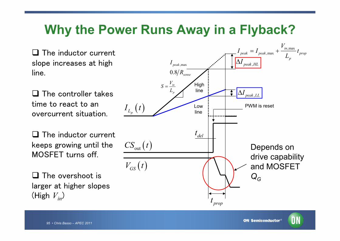
Why the Power Runs Away in a Flyback?
,max
0.8
peak
sense
I
R
in
p
VS
L
propt
delt
,max
,max
in
peak peak prop
p
VI I t
L
pLI t
outCS t
GSV t
PWM is reset
,peak LLIHighline
Lowline
Depends on drive capability and MOSFET QG
,peak HLI The inductor current slope increases at high line.
The controller takes time to react to an overcurrent situation.
The inductor current keeps growing until the MOSFET turns off.
The overshoot is larger at higher slopes (High Vin)

96 • Chris Basso – APEC 2011
The Effect in a DCM Converter
A flyback converter operated in DCM obeys the formula:
2,max
1
2out p peak swP L I F
Primary inductor
Max. peak current in fault
Switching frequency
Converter efficiency
As Lp and Fsw are fixed, Ipeak,max changes with line input
,
,max,
insensepeak LL prop
sens
L
e p
LVVI t
R L
,maxpeakI
pI L
,
,max,
insensepeak HL prop
sens
L
e p
HVVI t
R L
Low line High line
, ,
,max,,
peak in HL in LL
p sensepeak HLin LL
prop sense
I V V
L VIV
t R
A 13.5% overshoot translates in a 28% power increase
2
1.13 1.28 ( is considered constant over the range)
t

97 • Chris Basso – APEC 2011
Lp = 250 µH, Vsense = 1 V, tprop = 350 ns, Vin,LL= 120, Vin,HL = 370 V, Rsense = 0.33 Ω, Fsw = 65 kHz
The Power Increases at High Line
100 200 300 40045
50
55
60
65
VinV
WoutP
46 W
63W
In this example, the converter stays DCM on the whole range.
17 WoutP
= 85% = 89%

98 • Chris Basso – APEC 2011
How to Compensate the Runaway? How do we compensate this excess of power? we reduce the maximum peak current at high line this is called Over Power Protection – OPP
peakI peakI
inV inV
,maxpeakI ,peak LLI
,peak HLI
HLLL
How to calculate the compensated high-line current? Equate low-line power with high-line power and solve for Ipeak
HLLL
2
,max, ,max,
1
2pout eak HHL p wL s HLP L FI
Solve for Ipeak
,maxpeak inI f V

99 • Chris Basso – APEC 2011
Reducing the Peak Current
,max,
,max,
2out LL
peak HL
p sw HL
PI
L F
The amplitude of the sensed voltage must reduce by:
The compensated setpoint must subtract the prop. delay
,
,max,
in HLsensepeak HL prop
sense p
VVI t
R L
The final inductor peak current must equal:
,
,max,
in HL
sense peak HL prop sense
p
VV V I t R
L
100 • Chris Basso – APEC 2011
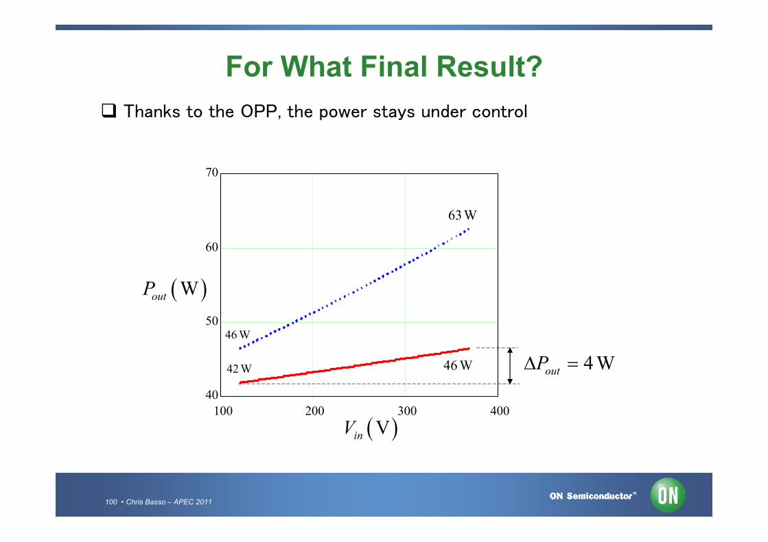
For What Final Result?
100 200 300 400
40
50
60
70
VinV
WoutP
46 W
63W
42 W 46 W 4 WoutP
Thanks to the OPP, the power stays under control

101 • Chris Basso – APEC 2011
The CCM Case is a Different Picture
In DCM, the valley current is zero, the stored energy is:
2,max
1
2p peakE L I
The peak current runaway, alone, affects the transmitted power
In CCM, the valley current changes the formula:
2 2,max
1
2p peak valleyE L I I
,maxpeakI
pI L
t
valleyI

102 • Chris Basso – APEC 2011
The Converter Changes its Operating Mode In fault mode, the converter operates in deep CCM at low line As the input voltage increases, the valley current decreases
Maximum current in fault
Maximum current in fault
pLI t
t
t
,minin
p
V
L
,maxin
p
V
L
out f
p
V V
NL
out f
p
V V
NL
,max,p LLI
,max,p HLI
, ,p valley LLI
, ,p valley HLI
,on LLt
,on HLt0
Low line
High line
LLE
HLE
HL LLE E

103 • Chris Basso – APEC 2011
Computing the Transmitted Power in CCM
First, we write the ton and toff equations in CCM
pLI t
t
,minin
p
V
L
out f
p
V V
NL
peakI
valleyI
ont offt
swT
inpeak valley on
p
VI I t
L
out f
valley peak off
p
V VI I t
NL
sw on offT t t
(1) (2) (3)

104 • Chris Basso – APEC 2011
Solving for the Valley Current
By combining the 3 equations, we have:
p peak valley
on
in
L I It
V
p peak valley
off sw on sw
in
L I It T t T
V
Replace toff in (2):
f out valley p peak p sw in
valley peak
p in
V V I L I L T VI I
L NV
Solve for Ivalley:
sw f out
valley peak
p f out
in
in
T VV VI I
L V V NV
,maxsense
peak prop
se se p
n
n
iVI t
R L
V
Max faultcurrent
sw in f out
L
p f out in
T V V VI
L V V NV
LL or HL
L peak valleyI I I

105 • Chris Basso – APEC 2011
Identifying the Operating Mode
Having the ripple on hand, we can confirm the mode:
Lon p
in
It L
V
L
off p
out f
N It L
V V
0
on off sw
valley
t t T
I
CCM
on off sw
sw off on
t t T
DT T t t
DCM
0
on off sw
valley
t t T
I
BCM
pLI t
DT
peakI
valleyI
peakI
peakI
ont
ont
ont
t
t
t

106 • Chris Basso – APEC 2011
Evaluating the Power in CCM Lp = 600 µH, Vsense = 1 V, tprop = 350 ns, Vin,LL= 120, Vin,HL = 370 V, Rsense = 0.33 Ω, Fsw = 65 kHz
2 2max, ,max, ,
176 W
2LL p peak LL valley LL sw LLP L I I F
2 2max, ,max, ,
1104 W
2HL p peak HL valley HL sw HLP L I I F
100 200 300 40070
80
90
100
110
VinV
WoutP 24 WoutP

107 • Chris Basso – APEC 2011
Reducing the Peak Current at High Line
If we lower the peak at high line, the ripple remains the same
pLI t
t
peakI
valleyI
ont offt
swT
peak CMPI
valleyCMPI
LILCMPI
22max, ,max, ,max, ,
1
2HL p peak HL peak HL L HL sw HLP L I I I F
0 in DCM
We can re-write the flyback power formula to include the ripple

108 • Chris Basso – APEC 2011
We Want to Limit the High-Line Power
We can force the high-line power to match that of low line
22max, ,max, ,max, ,
1
2LL p peak HL peak HL L HL sw HLP L I I I F
From there, we can extract the compensated peak current value
2, max,
,max,
,
2
2
sw p HL L HL LL
peak HL
sw p HL L HL
F L I PI
F L I
As this is the new setpoint, prop. delay contribution must be removed
,
,max,
in HL
sense peak HL prop sense
p
VV V I t R
L
After compensation, the peak current setpoint at high line becomes
,
,max,
in HLsensepeak HL prop
sense p
VV VI t
R L

109 • Chris Basso – APEC 2011
What is the Final Result?
The high line power now respects the LPS limit
100 200 300 40060
70
80
90
100
110
VinV
WoutP75 W
104 W
70 W
76 W
6 WoutP

110 • Chris Basso – APEC 2011
What Practical Solutions? There are several possibilities to reduce the peak current
1. Offset the current sense signal in the CS pin:
High line
2. Reduce the peak limit as Vin increases
,maxpeakI
pI L
t
,L LLI ,L HLI• easy to do
• affects the no-load stand-by power
• affects light-load efficiency
• implemented at IC level
• does not affect the no-load stand-by power
• does not affect light-load efficiency
,max,peak LLI
pI L
tHigh line
,max,peak HLI,L LLI
,L HLI
111 • Chris Basso – APEC 2011
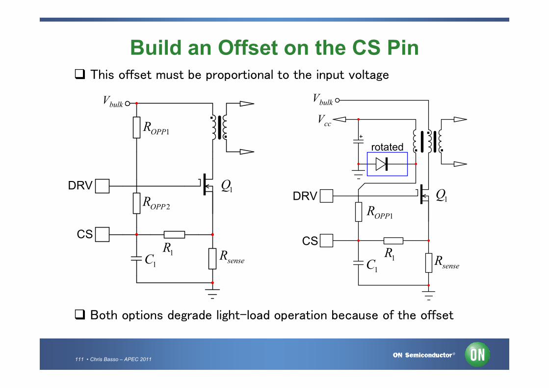
Build an Offset on the CS Pin
1Q
senseR1R1C
2OPPR
1OPPR
DRV
CS
Vbulk
Both options degrade light-load operation because of the offset
This offset must be proportional to the input voltage
..
DRV
CS
Vbulk
Vcc ...
1Q
senseR1R1C
1OPPR
rotated

112 • Chris Basso – APEC 2011
OPP Implementation in the NCP1250
+
. 0.8V 0.8V
41
PWM reset
CSOPP
Aux.
0
-200 mVon
off
0
800 mV
600 mVon
off
300-nsblank
OPPUR
OPPLR
The NCP1250 implement a non-dissipative OPP circuitry
The auxiliary swings to –Vin and reduces the setpoint OPP

113 • Chris Basso – APEC 2011
Checking the Results
Let us check on a real 19-V adapter built with the NCP1250
Lp = 600 µH, Vsense = 1 V, tprop = 350 ns, Vin,LL= 120, Vin,HL = 370 VRsense = 0.33 Ω, Fsw = 65 kHz, Vclamp = 90 V, ll = 2.2 µH, N = 0.25
Without any OPP compensation, we have:
,max, 4.1Aout LLI ,max, 5.7 Aout HLI
Once OPP has been implemented:
, ,72 W so 3.8 Aout LL out LLP I , ,78 W so 4.1Aout HL out HLP I

114 • Chris Basso – APEC 2011
Course Agenda
The Flyback Converter
The Parasitic Elements
How These Parasitics Affect your Design?
Current-Mode is the Most Popular Scheme
Fixed or Variable Frequency?
More Power than Needed
The Frequency Response
Compensating With the TL431
115 • Chris Basso – APEC 2011
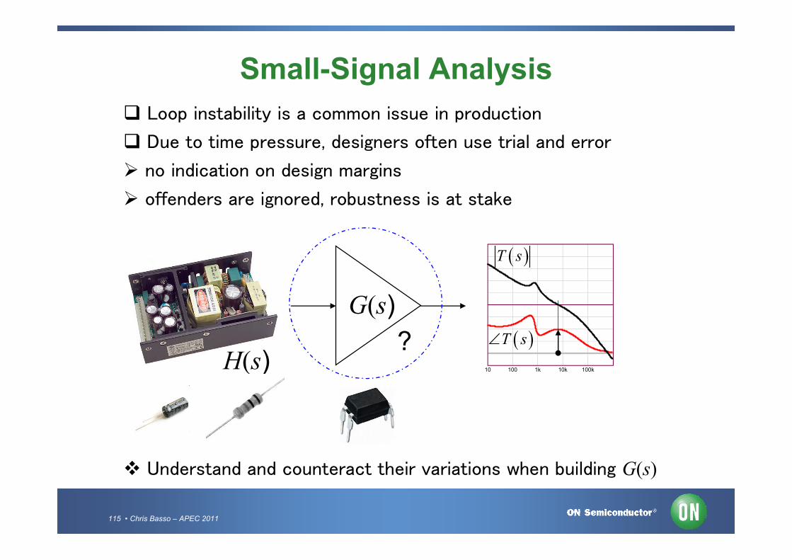
Small-Signal Analysis
Loop instability is a common issue in production
Due to time pressure, designers often use trial and error
no indication on design margins
offenders are ignored, robustness is at stake
G(s)
10 100 1k 10k 100k
T s
T s?H(s)
Understand and counteract their variations when building G(s)

116 • Chris Basso – APEC 2011
There are Two Options
Analytical analysis of the power stage:
best to see where the offenders are hidden (ESR, opto pole etc.)
equations are complex but litterature abounds
transfer function are for DCM or CCM
difficult to predict transient response
SPICE models:
easy-to-implement averaged models
can work in ac or transient mode
easily transition between CCM and DCM
do not explictly disclose the position of poles and zeros
A measurement on the bench is mandatory, whatever you choose!

117 • Chris Basso – APEC 2011
Analytical Analysis
You must first characterize the "plant" transfer function what are your power stage ac characteristics?
H(s)+
G(s)refV outV svc(s)
out outI s Z s
inin VV s G s
+
+
-d(s)
Plant
Compensator
out
c
V sH s
v s
outV sH s
d s
Current-mode control Voltage-mode control

118 • Chris Basso – APEC 2011
How do we Stabilize a Converter?
We need a high gain at dc for a low static error We want a sufficiently high crossover frequency for response speed Shape the compensator G(s) to build phase and gain margins!
m = 92°
10 100 1k 10k 100k 1Meg
-180°
0° - 0 dB
T s
T s
GM = 67 dB-88°
67T s dB
fc = 6.5 kHz

119 • Chris Basso – APEC 2011
How much phase margin to chose?
0 25 50 75 1000
2.5
5
7.5
10
76°
Q
m
5.00u 15.0u 25.0u 35.0u 45.0u
200m
600m
1.00
1.40
1.80
Q = 0.1
Q = 0.5
Q = 0.707
Q = 1
Q = 5
Fast response and no overshoot!
Q < 0.5 over dampingQ = 0.5 critical dampingQ > 0.5 under damping
Asymptotically stable
Q = 0.5
a Q factor of 0.5 (critical response) implies a m of 76° a 45° m corresponds to a Q of 1.2: oscillatory response!
phase margin depends on the needed response: fast, no overshoot… good practice is to shoot for 60° and make sure m always > 45°

120 • Chris Basso – APEC 2011
What Compensator Types do we Need?
There are basically 3 compensator types:
type 1, 1 pole at the origin, no phase boost
type 2, 1 pole at the origin, 1 zero, 1 pole. Phase boost up to 90°
type 3, 1 pole at the origin, 1 zero pair, 1 pole pair. Boost up to 180°
10 100 1k 10k 100k
G s
G s
270
boost
1 2 5 10 20 50 100 200 500 1k
270G s
G s
10 100 1k 10k 100k
G s
G s
270
boost
Type 1 Type 2 Type 3

121 • Chris Basso – APEC 2011
Fixed-Frequency Current-Mode
2
, 22load in
p critoutsw
in
R VL
VF N VN
Lp > Lp,crit ? Yes, CCM else DCM
Assume CCM, compute the duty-ratio: out
out in
VD
V NV
Compute M and : L22 pout
L
in load sw
L NVM
NV R T
First, check the operating mode, CCM or DCM?
Evaluate the dc gain and poles/zeros positions:
0 2
1
12 1
load
sense FB
L
RG
R G N DM

122 • Chris Basso – APEC 2011
Fixed-Frequency Current-Mode
Check the quality coefficient at Fsw/2
inn sense
p
VS R
L 1e c nS M S
1 = no compensation
1
1 0.5p
c
QM D
Apply to formula to plot the ac response:
1 20 2
2
1
1 11
11
z z
n p np
s s
H s Gs ssQ
1 ec
n
SM
S n
swT
Compute the poles/zeros positions:
2
2
2
1
2
load
z
p
D Rf
DL N
1
1
2z
tR ouESRf
C
1
31
1
2L
p
load out
DD
fR C
3rd order

123 • Chris Basso – APEC 2011
Fixed-Frequency Current-Mode
2
1
22
1
10 0 2 2 22
1 11
20log
1 1
z z
p n n p
f f
f fH f G
f f ff f f Q
Extract the magnitude and the argument definitions
1 2 1
1 1 1 1
2
1arg tan tan tan tan
1z p n pz
n
f f f fH f
f f f Qf f
f
Plot them with Mathcad® for instance.
RHPZ
124 • Chris Basso – APEC 2011
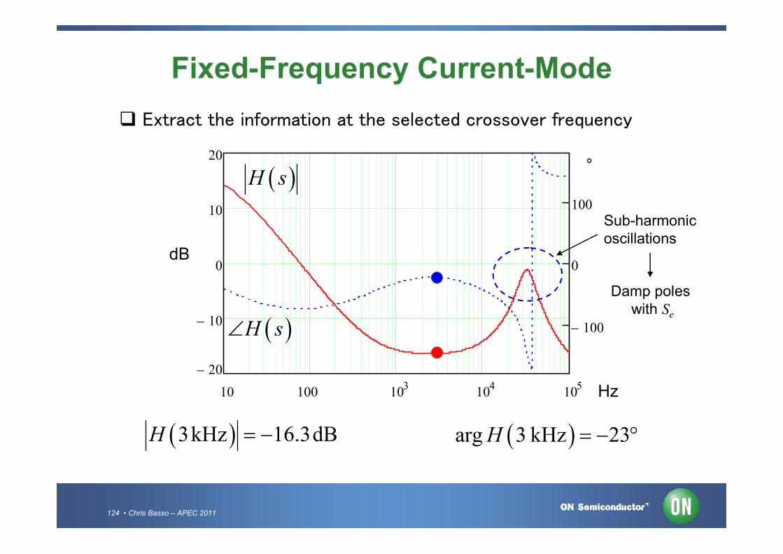
Fixed-Frequency Current-Mode
10 100 103
104
105
20
10
0
10
20
100
0
100
Extract the information at the selected crossover frequency
H s
H s
3kHz 16.3dBH arg 3 kHz 23H
dB
Hz
Sub-harmonicoscillations
Damp poles with Se
°

125 • Chris Basso – APEC 2011
Fixed-Frequency Current-Mode
The compensation strategy is the following:
compensate the gain loss at fc so that:
evaluate the boost in phase at fc to get phase 70° margin:
3kHz 16.3dBG
Boost PM argH 90 3.15cf
Boost = 0 select type 1 – origin poleBoost < 90° select type 2 – origin pole, 1 pole, 1 zero
k-factor can be used to place the pole and the zero
tan 45 12
boostk
poles and zeros are coincident
1 1 3 3 kHzpk cf kf k 1
33 kHz
1c
zk
f kf
k
126 • Chris Basso – APEC 2011
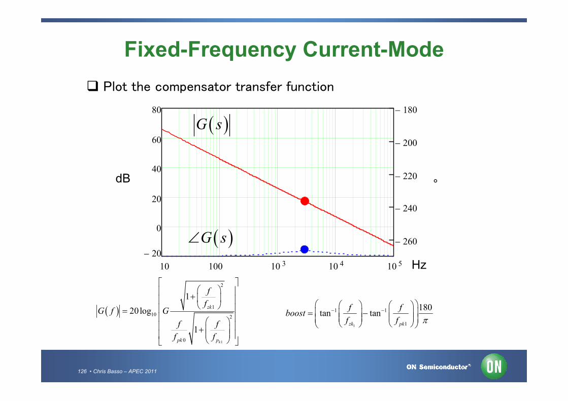
Fixed-Frequency Current-Mode
Plot the compensator transfer function
10 100 10 3 10 4 10 5
20
0
20
40
60
80
260
240
220
200
180
G s
G s
dB
Hz
1
2
1
10 2
0
1
20log
1k
zk
pk p
f
fG f G
f f
f f
1
1 1
1
180tan tan
zk pk
f fboost
f f
°

127 • Chris Basso – APEC 2011
Fixed-Frequency Current-Mode
Plot the loop gain transfer function and check the margins
10 100 103 104 105
50
0
50
100
300
200
100
0
360
T s
T s
dB
Hz
fc = 3 kHz
70m
°
Sweep ESR, Cout, Rload and verify the results

128 • Chris Basso – APEC 2011
Fixed-Frequency Current-Mode
In case the converter transitions to DCM, update the equation!
10 100 103 104 10530
20
10
0
10
20
50
0
50
H s
H s
1 2
1 2
0
1 1
1 1
z z
p p
s s
H s Gs s
Yes, analytical analysis is long and tedious. But, it teaches where the threats are and how to deal with!

129 • Chris Basso – APEC 2011
Variable-Frequency Current-Mode
Observing the waveforms helps us to derive an average model
a c
p
Vc/(2*Ri)d1.Ic
Ia Ic It gives birth to a large-signal model
peakI
swdT
aI t cI t
swT
peakI
2sw
peak
c T
II t
2 i out out in
c
in out
R P V NVV
V V
1c p
sw
i in out
V L NT
R V V
1
2 out i
c in
P Rd
V V
Senseresistor
130 • Chris Basso – APEC 2011
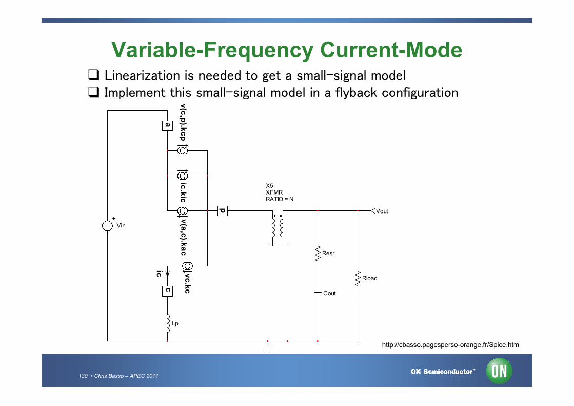
Variable-Frequency Current-Mode Linearization is needed to get a small-signal model Implement this small-signal model in a flyback configuration
ac
p
vc.k
cv
(c,p
).kcp
ic.k
icv
(a,c
).kac
ic
X5XFMRRATIO = N
Resr
Cout
Rload
Vout
Lp
Vin
http://cbasso.pagesperso-orange.fr/Spice.htm

131 • Chris Basso – APEC 2011
Variable-Frequency Current-Mode Derive the transfer function and isolate poles and zeros
0
1
21
11ˆ
ˆ1
zout z
c
p
s
s
s
v s sG
v s s
s
02
2 1
load
outi
in
R DivG
VNR
NV
1
1 2 1
2 1p
load out
Mf
R C M
1
1
2z
ESR out
fR C
2 2
1
2 1load
z
p
Rf
N L M M
1 10 100 103
104
105
0
5
10
15
100
80
60
40
20
0
Then plot the function
dB °
Hz
H s
H s
Tailor G(s) to getthe desired fc
1st order

132 • Chris Basso – APEC 2011
Use a SPICE Model to Stabilize the Converter
1
C52m
R1015m
2
Vin340AC = 0
18 4
X2xXFMRRATIO = -250m
vout
16DC
13
LpLp
D1Ambr20200ctp
20
L12.2u
R120m voutvint
6
27
C1220u
R1585m
parameters
Vout=19
Ibridge=250uRlower=2.5/IbridgeRupper=(Vout-2.5)/Ibridge
Lp=600uFs=70kRsense=0.5Se=0
fc=1kpm=60Gfc=-21pfc=-88
G=10^(-Gfc/20)boost=pm-(pfc)-90pi=3.14159K=tan((boost/2+45)*pi/180)
Fzero=fc/kFpole=k*fc
Rpulldown=4.7kRLED=CTR*Rpulldown/GCzero=1/(2*pi*Fzero*Rupper)Cpole=1/(2*pi*Fpole*Rpulldown)
CTR=0.9Pole=15k
B1Voltage
(V(err)-1.2)/3 > 1 ?1 : (V(err)-1.2)/3
15
14
CoL1kF
VstimAC = 1
8 5
LoL1kH
2V5gnd
UC384X
19
X3OP384X1
R247k
R347k
err
Rload20
vca
c
PW
M s
witch C
Mp
duty
-cyc
le
X9PWMCML = LpFs = FsRi = RsenseSe = Se
9
Vdd5
10
11
X10TL431_G
Rupper2Rupper
Rlower2Rlower
RledRLED
Czero1Czero
vout
Cpole2Cpole
X7OptocouplerCpole = 1/(6.28*pole*pullup)CTR = CTR
vint
R4Rpulldown
Verr
19.0V
19.0V
340V
-78.4V 19.6V
19.0V
116mV
0V
19.0V
19.0V
470mV
2.39V
0V
2.39V 2.39V
2.50V
2.61V
5.00V
17.6V
2.49V
18.8V Cannot be beaten for simplicity and speed!
Automate the compensation!
133 • Chris Basso – APEC 2011
Unveil the Transfer Function in a Second
-40.0
-20.0
0
20.0
40.0
10 100 1k 10k 100k
-180
-90.0
0
90.0
180
-60.0
-30.0
0
30.0
60.0
dB °
-180
-90.0
0
90.0
180
dB °
H s
H s
T s
T s
Loop gain
Power stage gain
m
fc

134 • Chris Basso – APEC 2011
Course Agenda
The Flyback Converter
The Parasitic Elements
How These Parasitics Affect your Design?
Current-Mode is the Most Popular Scheme
Fixed or Variable Frequency?
More Power than Needed
The Frequency Response
Compensating With the TL431

135 • Chris Basso – APEC 2011
How is regulation performed?
Text books only describe op amps in compensators…
outV
errV
The market reality is different: the TL431 rules!
TL431 optocoupler
errV
outVI’m the
law!

136 • Chris Basso – APEC 2011
The TL431 Programmable Zener
The TL431 is the most popular choice in nowadays designs
It associates an open-collector op amp and a reference voltage
The internal circuitry is self-supplied from the cathode current
When the R node exceeds 2.5 V, it sinks current from its cathode
2.5V
K
A
R
TL431A
K
A
R
RAK
The TL431 is a shunt regulator

137 • Chris Basso – APEC 2011
A Rabbit and a (French) Snail…
The TL431 lends itself very well to optocoupler control
lowerR
1RLEDR
biasR
outV
FBV
ddV
2C1C
TL431
outV
1I
LEDI
1I
min 2.5V V
1fV V
1bias
bias
VI
R
biasR
RLED must leave enough headroom over the TL431: upper limit!
LEDR
Fast lane Slow lane
dc representation
pullupR

138 • Chris Basso – APEC 2011
Understanding the Fast Lane Drawback
This LED resistor is a design limiting factor in low output voltages:
431,min
,max min
, min
CTRCTR
out f TL
LED pullup
dd CE sat bias pullup
V V VR R
V V I R
When the capacitor C1 is a short-circuit, RLED fixes the fast lane gain
outV s
LEDR
pullupR
ddV
1I
cI0 V
in ac
FBV s
1( ) CTRFB pullupV s R I
1
( )out
LED
V sI
R
( )CTR
( )
pullupFB
out LED
RV s
V s R
This resistor plays a role in dc too!
lowerR
1R

139 • Chris Basso – APEC 2011
The Static Gain Limit
Let us assume the following design:
,max
5 1 2.520k 0.3
4.8 0.3 1 0.3 20LEDR
m k
431,min
,
min
5
1
2.5
4.8
300
1
CTR 0.3
20
out
f
TL
dd
CE sat
bias
pullup
V V
V V
V V
V V
V mV
I mA
R k
,max 857LEDR
0
20CTR 0.3 7 17
0.857
pullup
LED
RG or dB
R
In designs where RLED fixes the gain, G0 cannot be below 17 dB
You cannot “amplify” by less than 17 dB
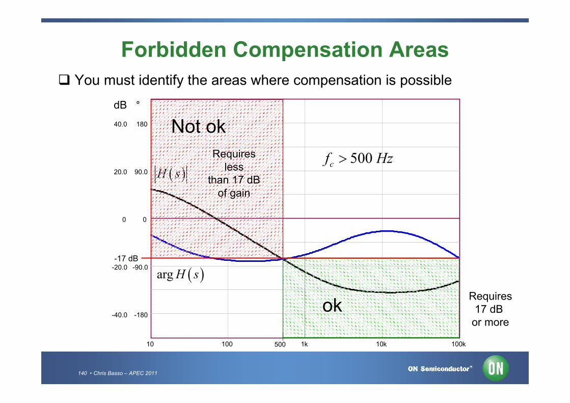
140 • Chris Basso – APEC 2011
Forbidden Compensation Areas
You must identify the areas where compensation is possible
10 100 1k 10k 100k
18040.0
-180
-90.0
0
90.0
-40.0
-20.0
0
20.0
dB °
arg H s
H s
-17 dB
500
500cf Hz
ok
Not ok
Requires17 dB
or more
Requiresless
than 17 dB of gain

141 • Chris Basso – APEC 2011
Injecting Bias Current
Make sure enough current always biases the TL431
If not, its open-loop suffers – a 10-dB difference can be observed!
Ibias = 1.3 mA
Ibias = 300 µA
> 10-dB difference
Easysolution
Ibias
Rbias
11
1biasR k
m
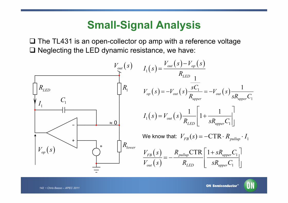
142 • Chris Basso – APEC 2011
Small-Signal Analysis
The TL431 is an open-collector op amp with a reference voltage
Neglecting the LED dynamic resistance, we have:
LEDR
lowerR
1R
outV s
1C1I
opV s
1
out op
LED
V s V sI s
R
1
1
1
1op out out
upper upper
sCV s V s V s
R sR C
0 1
1
1 11out
LED upper
I s V sR sR C
We know that:1( ) CTRFB pullupV s R I
1
1
CTR 1pullup upperFB
out LED upper
R sR CV s
V s R sR C

143 • Chris Basso – APEC 2011
Creating a High-Frequency Pole In the previous equation we have:
a static gain
a 0-dB origin pole frequency
a zero
We are missing a pole for the type 2!
1
1
1z
upperR C
1
1po
upperC R
pullupR
2C
FBV s
0 = CTRpullup
LED
RG
R
ddV
Add a cap. fromcollector to ground
1
1 2
CTR 1
1
pullup upperFB
out LED upper pullup
R sR CV s
V s R sR C sR C
Type 2 transfer function
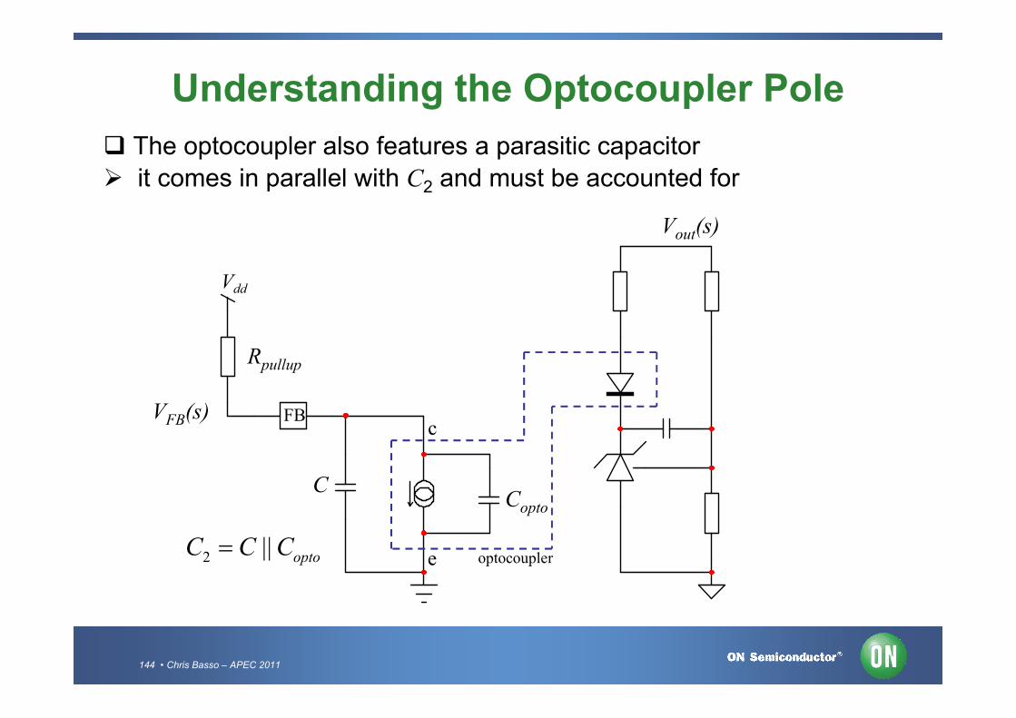
144 • Chris Basso – APEC 2011
Understanding the Optocoupler Pole
The optocoupler also features a parasitic capacitor
it comes in parallel with C2 and must be accounted for
FBc
e
Rpullup
C
Vdd
VFB(s)
Vout(s)
optocoupler
Copto
2 || optoC C C

145 • Chris Basso – APEC 2011
Extracting the Pole
The optocoupler must be characterized to know where its pole is
2
1
Rpullup20k
Vdd5
3
X1SFH615A-4
4
Vbias
RbiasVFB
6
Vac
5
Cdc10uFIc
Rled20k
IF
Adjust Vbias to have VFB at 2-3 V to be in linear region, then ac sweep
The pole in this example is found at 4 kHz
-3 dB
O s
O s
1 12 nF
2 6.28 20 4opto
pullup pole
CR f k k
Another designconstraint!
4 k

146 • Chris Basso – APEC 2011
The TL431 in a Type 1 Compensator
To make a type 1 (origin pole only) neutralize the zero and the pole
1
1 2
CTR 1
1
pullup upperFB
out LED upper pullup
R sR CV s
V s R sR C sR C
1 2upper pullupsR C sR C1 2
pullup
upper
RC C
R
1
1
CTR
poupper LED
pullup
R RC
R
substitute
2
CTRpo
LEDC R
2
CTR
2 po LED
Cf R
Once neutralized, you are left with an integrator
1
po
G ss
| | po
c
c
fG f
f
cpo f cf G f 2
CTR
2cf c LED
CG f R

147 • Chris Basso – APEC 2011
A Type 1 Design Example
We want a 5-dB gain at 5 kHz to stabilize the 5-V converter
431,min
,
min
5
20
5 V
1 V
2.5 V
4.8 V
300 mV
1 mA
CTR 0.3
20 kΩ
10 1.77
5 kHz
out
f
TL
dd
CE sat
bias
pullup
fc
c
V
V
V
V
V
I
R
G
f
,max 857LEDR 728LEDR
Apply 15%margin
2
CTR 0.37.4 nF
2 6.28 1.77 5 728cf c LED
CG f R k
Copto = 2 nF
7.4 2 5.4 nFC n n 1 2 14.7 nFpullup
upper
RC C
R

148 • Chris Basso – APEC 2011
Simulation of the Type 1
SPICE can simulate the design – automate elements calculations…
3
1
4
X2OptocouplerCpole = CoptoCTR = CTR
5
RLEDRLED
2
R2Rupper
R310k
6
RpullupRpullup
CpoleCpole
VddVdd
VFB
7
L11k
9
E1-1k
V22.5
10
C31k
V3AC = 1
R5100m
X1TL431_G
B1Voltage
err
C1C1
V(err)<0 ?0 : V(err)
R61k
3.97V
2.96V
2.50V
4.99V
2.50V
4.80V 4.99V 4.99V
2.50V
4.99V
0V
parameters
Vout=5
Vf=1Vref=2.5VCEsat=300mVdd=4.8Ibias=1m
A=Vout-Vf-VrefB=Vdd-VCEsat+Ibias*CTR*RpullupRmax=(A/B)*Rpullup*CTR
Rupper=(Vout-2.5)/250ufc=5kGfc=-5
G=10^(-Gfc/20)pi=3.14159
Fpo=G*fc
Rpullup=20k
RLED=Rmax*0.85
C1=Cpole1*Rpullup/Rupper
Cpole1=CTR/(2*pi*Fpo*RLED)Cpole=Cpole1-Copto
Fopto=4kCopto=1/(2*pi*Fopto*Rpullup)CTR = 0.3
Automatic biaspoint selection

149 • Chris Basso – APEC 2011
Type 1 Simulation Results
The pullup resistor is 1 k and the target now reaches 5 dB
-20.0
-10.0
0
10.0
20.0
100 200 500 1k 2k 5k 10k 20k 50k 100k
-90.0
0
90.0
180
270
arg G s
G s
5 dB
dB
°
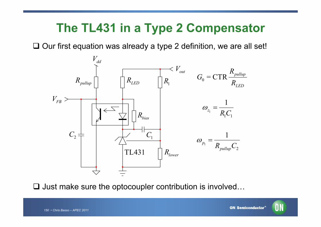
150 • Chris Basso – APEC 2011
The TL431 in a Type 2 Compensator
Our first equation was already a type 2 definition, we are all set!
lowerR
1RLEDR
biasR
outV
FBV
ddV
2C1C
TL431
pullupR
1
1 1
1z
R C
0 = CTRpullup
LED
RG
R
1
2
1p
pullupR C
Just make sure the optocoupler contribution is involved…

151 • Chris Basso – APEC 2011
Deriving Component Values for the Type 2
You need to provide a 15-dB gain at 5 kHz with a 50° boost
15 200 = CTR 10 5.62
pullup
LED
RG
R
With a 250-µA bridge current, the divider resistor is made of:
2.5 250 10 kΩlowerR u 1 12 2.5 250 38 kΩR u
The pole and zero respectively depend on Rpullup and R1:
1 11 2 2.3 nFzC f R 2 1 2 581 pFp pullupC f R
The LED resistor depends on the needed mid-band gain:
0
CTR1.06 kΩ
pullup
LED
RR
G ,max 4.85 kΩLEDR ok
2tan tan 1 2.74 5 13.7 kHzp cf boost boost f k
2 25 13.7 1.8 kHzz c pf f f k k

152 • Chris Basso – APEC 2011
Checking the Optocoupler Contribution
The optocoupler is still at a 4-kHz frequency:
2 nFpoleC
Type 2 pole capacitor calculation requires a 581-pF cap.!
The bandwidth cannot be reached, reduce fc!
For noise purposes, we want a minimum of 100 pF for C
With a total capacitance of 2.1 nF, the highest pole can be:
1 13.8 kHz
2 6.28 20 2.1pole
pullup
fR C k n
For a 50° phase boost and a 3.8-kHz pole, the crossover must be:
21.4 kHz
tan tan 1
p
c
ff
boost boost
Already above!

153 • Chris Basso – APEC 2011
Placing the Zero in the Transfer Function
The zero is then simply obtained:2
516 Hzcz
p
ff
f
We can re-derive the component values and check they are ok
1 11 2 8.1 nFzC f R 2 1 2 2.1 nFp pullupC f R
Given the 2-nF optocoupler capacitor, we just add 100 pF
In this example, RLED,max is 4.85 k
0
20CTR 0.3 1.2 1.8 dB
4.85
pullup
LED
RG or
R
You cannot use this type 2 if an attenuation is required at fc!

154 • Chris Basso – APEC 2011
TL431 type 2 Design Example
The 1-dB gain difference is linked to Rd and the bias current
-10.0
0
10.0
20.0
30.0
10 100 1k 10k 100k
100
110
120
130
140 arg G s
G s
14 dB @ 1.4 kHz
dB
°
50°

155 • Chris Basso – APEC 2011
Design Example 1 – a Single-Stage PFC The single-stage PFC is often used in LED applications
It combines isolation, current-regulation and power factor correction
Here, a constant on-time BCM controler, the NCP1608, is used
1
4
2Dc
5Fsw
6Ip
L1L
3
R1100m
7 8
X2XFMRRATIO = -250m
9
R250m
C12.2mF
13
15
X3TLV431
1617
X4OptocouplerCpole = CoptoCTR = CTR
23
Rsense0.5
10
R4Rupper
14
R5RLED
18
R6Rpullup
VddVdd
C2C2
parameters
Vrms=100L=400u
Ct=1.5nIcharge=270uGpwm=(Ct/Icharge)*1Meg
19
GA
IN
22
X5K = GpwmGAIN
28
C4C1
50 V2 A string
Vout
R765k
D41N965
C50.1uF
vca
c
PW
M s
witc
h B
CM
p
du
ty-c
ycle
Fsw
(kH
z)Ip
X1PWMBCMVML = L
VFB
ILED
R9R2
11
V1Vrms*1.414
B1Voltage
29
LoL1k
20
CoL1k
AC = 1V3
errac
VsenseV(errac)-0.6
598mV
68.4V
3.09V
0V
154mV
-210V 52.5V
52.5V
11.1V
1.24V
12.2V2.17V
1.24V
1.24V15.1V
5.00V
1.57V
8.74V
1.24V
141V
26.9V
2.17V
2.17V
0V
ac in
Ac out
Iout = 2.4 A
On-timeselection
1 V = 1 µs
Average simulation
1.25 V

156 • Chris Basso – APEC 2011
Design Example 1 – a Single-Stage PFC Once the converter elements are known, ac-sweep the circuit
Select a crossover low enough to reject the ripple, e.g. 20 Hz
-8.00
-4.00
0
4.00
8.00
0
1 2 5 10 20 50 100 200 500 1k
-80.0
-40.0
0
40.0
80.0
-2.5 dB20 Hz
-11° arg H s
H s
dB
°

157 • Chris Basso – APEC 2011
4
5
67
3
10
11
12
1
13
2
Design Example 1 – a Single-Stage PFC Given the low phase lag, a type 1 can be chosen
Use the type 2 with fast lane removal where fp and fz are coincident
G s
6.1 kΩ 10 kΩ
13.6 kΩ586 nF395 nF
20 kΩton
generation
15 V
-20.0
-10.0
0
10.0
20.0
1 2 5 10 20 50 100 200 500 1k
-180
-90.0
0
90.0
180
fc = 19 Hz
m = 90°
argT s
T s
0.5
5 V
dB
°

158 • Chris Basso – APEC 2011
Design Example 1 – a Single-Stage PFC
-2.00
0
2.00
4.00
6.00
3.40
3.80
4.20
4.60
5.00
20.0m 60.0m 100m 140m 180m
-4.00
-2.00
0
2.00
4.00
A transient simulation helps to test the system stability
LEDI t
FBV t
inI t
2.2 A
Vin = 100 V rms

159 • Chris Basso – APEC 2011
Design Example 2: a DCM Flyback Converter
We want to stabilize a 20-W DCM adapter
Vin = 85 to 265 V rms, Vout = 12 V/1.7 A
Fsw = 65 kHz, Rpullup = 20 kΩ
Optocoupler is SFH-615A, pole is at 6 kHz
Cross over target is 1 kHz
Selected controller: NCP1216
1. Obtain a power stage open-loop Bode plot, H(s)
2. Look for gain and phase values at cross over
3. Compensate gain and build phase at cross over, G(s)
4. Run a loop gain analysis to check for margins, T(s)
5. Test transient responses in various conditions

160 • Chris Basso – APEC 2011
Design Example 2: a DCM Flyback Converter
Capture a SPICE schematic with an averaged model
1
C53mF
R1020m
2
Vin90AC = 0
3 4
X2xXFMRRATIO = -166m vout
vout
6DC
8
13
L1Lp
D1Ambr20200ctp
B1Voltage
V(errP)/3 > 1 ?1 : V(errP)/3
Rload7.2
vca
c
PW
M s
witc
h C
Mp
duty
-cyc
le
X9PWMCML = LpFs = 65kRi = 0.7Se = Se
12.0V
12.0V90.0V
-76.1V 12.6V
389mV
0V
839mV
Look for the bias points values: Vout = 12 V, ok
Coming from FB

161 • Chris Basso – APEC 2011
Design Example 2: a DCM Flyback Converter Observe the open-loop Bode plot and select fc: 1 kHz
10 100 1k 10k 100k
18040.0
Magnitude at 1 kHz-23 dB
Phase at 1 kHz-70 °
-180
-90.0
0
90.0
-40.0
-20.0
0
20.0
dB °
arg H s
H s

162 • Chris Basso – APEC 2011
Design example 2: a DCM flyback converter
Apply k factor or other method, get fz and fp
fz = 3.5 kHz fp = 4.5 kHz
1.3nFoptoC
3.8nFC
2 3.8 1.3 2.5nFC n n
2.5nF
20 kΩ
k factorgave
install
FB
Vdd
VFB(s)
Vout(s)
38kΩ
10 kΩ
2 kΩ
10 nF

163 • Chris Basso – APEC 2011
Design example 2: a DCM Flyback Converter
4
m = 60°
Check loop gain and watch phase margin at fc
10 100 1k 10k 100k
-80.0
-40.0
0
40.0
80.0
-180
-90.0
0
90.0
180
Crossover1 kHz
dB°
argT s
T s

164 • Chris Basso – APEC 2011
Design Example 2: a DCM Flyback Converter
Sweep ESR values and check margins again
3.00m 9.00m 15.0m 21.0m 27.0m
11.88
11.92
11.96
12.00
12.04
Lowline
Highline
100mV
200 mA to 2 A in 1 A/µs
Vout(t)

165 • Chris Basso – APEC 2011
Conclusion
The flyback converter hides several parasitic elements
Understanding where they hide and how they move is key!
Despite CM overwhelming presence, QR designs grow
CM is a 3rd-order system whereas QR is 1st order
TL431 lends itself well for compensation, watch the optocoupler!
SPICE eases and speed-up the design
Always check theoretical assumptions with bench measurement
Merci !Thank you!
Xiè-xie!