the development of high dielectric constant …
TRANSCRIPT
THE DEVELOPMENT OF HIGH DIELECTRIC CONSTANT COMPOSITE
MATERIALS AND THEIR APPLICATION IN A COMPACT HIGH POWER
ANTENNA
_______________________________________
A Dissertation
presented to
the Faculty of the Graduate School
at the University of Missouri-Columbia
_______________________________________________________
In Partial Fulfillment
of the Requirements for the Degree
Doctor of Philosophy
_____________________________________________________
by
KEVIN A. O’CONNOR
Dr. Randy Curry, Dissertation Supervisor
May 2013

© Copyright by Kevin A. O’Connor 2013
All Rights Reserved

The undersigned, appointed by the dean of the Graduate School, have examined the
dissertation entitled
THE DEVELOPMENT OF HIGH DIELECTRIC CONSTANT COMPOSITE
MATERIALS AND THEIR APPLICATION IN A COMPACT HIGH POWER
ANTENNA
presented by Kevin A. O’Connor, a candidate for the degree of Doctor of Philosophy in
Electrical and Computer Engineering,
and hereby certify that, in their opinion, it is worthy of acceptance.
Professor Randy Curry
Professor Robert Druce
Professor Justin Legarsky
Professor Gregory Triplett
Professor Thomas Clevenger

This work is dedicated to the members of the US Armed Forces who served in response
to the terrorist attacks of September 11, 2001.
I am sincerely thankful for the support provided to me by my family and friends
throughout this process. In particular, I appreciate the love, support, and patience of my
wife, Karen, during the last few years. The support and encouragement offered to me by
my immediate and extended families during this effort have been very helpful.

ii
ACKNOWLEDGEMENTS
I first and foremost must express my appreciation to my dissertation supervisor, Dr.
Randy Curry. Dr. Curry introduced me to the fields of research in which I have become
so deeply involved. He provided guidance, advice, and encouragement when needed
while also creating an environment in which independent thought and innovation is
supported. The Center for Physical and Power Electronics that Dr. Curry founded and led
during my graduate studies has been an excellent institution in which to study,
experiment, and cultivate a spirit for innovation.
I would also like to thank the members of my dissertation committee for their service.
Each member of the committee has research interests in specific areas relating to this
work, so their review and guidance is very much appreciated.
I wish to thank Dan Crosby for managing the chemical lab in which the materials were
produced and for his work in preparing many samples both in the materials development
and testing phases of the program. Bill Carter, Vicki Edwards, and Mike Fulca provided
great logistical support in lab management and equipment procurement. The rest of
technical staff at the Center have been very supportive and encouraging, including Dr.
Robert Druce, Dr. Ryan Karhi, Dr. David Bryan, and Dr. Dennis Pease. Mr. Lou Ross
must be recognized for his assistance with the scanning electron microscope, and Dr.
Stephen Lombardo generously provided the use of his laboratory’s high temperature
furnaces.
I have had the pleasure to work and become friends with many great graduate and
undergraduate students during my PhD studies. Although I cannot single out them all, I
would like to specifically mention the other PhD students I have studied and worked
with, including Peter Norgard, Chris Yeckel, and Adam Lodes. The conversations and
shared experiences with these peers have been very valuable.

iii
TABLE OF CONTENTS
LIST OF FIGURES ........................................................................................................... ix
LIST OF TABLES ........................................................................................................... xvi
ABSTRACT ................................................................................................................... xviii
Chapter 1: Introduction ....................................................................................................... 1
1.1 Motivation ........................................................................................................... 1
1.1.1 Size Limitation of Antennas .............................................................................. 1
1.1.2 Material Requirements ....................................................................................... 5
1.2 Research Goals........................................................................................................ 11
1.3 Overview ................................................................................................................. 13
References for Chapter 1 .............................................................................................. 16
Chapter 2: Critical Issues in the Development of Composite Materials Combining High
Dielectric Constant and High Dielectric Strength ............................................................ 17
2.1 Complex Permittivity and the Dielectric Constant ................................................. 17
2.2 The Effective Dielectric Constant of Composites .................................................. 25
2.2.1 Background on the Effective Dielectric Constant ........................................... 25
2.2.2 Mathematical Models....................................................................................... 26
2.2.3 Three-Dimensional Electrostatic Modeling ..................................................... 29
2.3 Particle Packing Density ......................................................................................... 34
2.4 Homogeneity ........................................................................................................... 53

iv
2.5 Factors Contributing to High Dielectric Strength ................................................... 62
2.5.1 Voids ................................................................................................................ 62
2.5.2 Air Gaps at Surface Contacts ........................................................................... 66
2.5.3 Triple Points ..................................................................................................... 68
References for Chapter 2 .............................................................................................. 73
Chapter 3: Development of High Dielectric Constant Composite Materials ................... 75
3.1 Literature Survey of High Dielectric Constant Composites ................................... 75
3.2 Novel Approaches to High Dielectric Constant Composite Development ............. 80
3.2.1 Trimodal Particle Packing................................................................................ 81
3.2.2 In-situ Polymerization ...................................................................................... 83
3.2.3 Void-Filling with High Dielectric Constant Fluids ......................................... 85
3.3 Concepts of the Classes of High Dielectric Constant Composites ......................... 86
3.3.1 Composite Class 1 – MU45 ............................................................................. 86
3.3.2 Composite Class 2 – MU100 ........................................................................... 87
3.3.3 Composite Class 3 – MU550 ........................................................................... 88
3.4 High Dielectric Constant Ceramics ........................................................................ 90
3.4.1 Overview of Perovskite Ceramics ................................................................... 90
3.4.2 Selection of Ceramic Material ......................................................................... 94
3.5 Binder Materials...................................................................................................... 96
3.5.1 Cyanoethylated Pullulan .................................................................................. 96
3.5.2 Polysilsesquioxanes ......................................................................................... 97
3.5.3 Agarose .......................................................................................................... 101

v
3.6 Void Fillers ........................................................................................................... 103
3.6.1 Survey of High Dielectric Constant Fluids .................................................... 103
3.6.2 Alkylene Carbonates ...................................................................................... 106
3.7 Examples and Physical Descriptions of Composites ............................................ 108
References for Chapter 3 ............................................................................................ 113
Chapter 4: Dielectric Materials Characterization ........................................................... 116
4.1 Introduction ........................................................................................................... 116
4.2 Dielectric Spectroscopy ........................................................................................ 117
4.2.1 Dielectric Spectroscopy Methods .................................................................. 117
4.2.2 Dielectric Spectroscopy Results .................................................................... 125
4.3 Polarization ........................................................................................................... 132
4.3.1 Polarization Methods ..................................................................................... 132
4.3.2 Polarization Results ....................................................................................... 136
4.4 Capacitive Discharge ............................................................................................ 141
4.4.1 Capacitive Discharge Methods ...................................................................... 141
4.4.2 Capacitive Discharge Results ........................................................................ 144
4.5 Dielectric Strength ................................................................................................ 147
4.5.1 Dielectric Strength Methods .......................................................................... 147
4.5.2 Dielectric Strength Results ............................................................................ 156
4.6 Thermogravimetric Analysis ................................................................................ 163
4.6.1 Thermogravimetric Analysis Methods .......................................................... 163
4.6.2 Thermogravimetric Analysis Results ............................................................. 166
vi
4.7 Scanning Electron Microscopy ............................................................................. 169
4.7.1 Scanning Electron Microscopy Methods ....................................................... 169
4.7.2 Scanning Electron Microscopy Results ......................................................... 171
4.8 3D Modeling of High Dielectric Constant Composites ........................................ 177
4.8.1 3D Model Description.................................................................................... 177
4.8.2 Model Results ................................................................................................ 183
References for Chapter 4 ............................................................................................ 190
Chapter 5: High Power Dielectric Resonator Antenna ................................................... 191
5.1 Background on Dielectric Resonator Antennas .................................................... 191
5.2 Coupling Methods ................................................................................................. 193
5.3 Resonant Modes a Cylindrical Dielectric Resonator ............................................ 197
5.4 Bandwidth Enhancement ...................................................................................... 208
5.5 DRA Design .......................................................................................................... 212
5.6 DRA Evaluation Methods ..................................................................................... 218
5.6.1 Simulation of the Antenna Reflection Coefficient and Radiation Pattern ..... 218
5.6.2 Low Voltage Measurements .......................................................................... 219
5.6.3 Comparison with Fundamental Limits for Electrically Small Antennas ....... 222
5.7 DRA Simulation and Experimental Results ......................................................... 224
5.7.1 Simulation Results ......................................................................................... 224
5.7.2 Low Power Experimental Results .................................................................. 232
5.7.3 Evaluation of Experimental Results against Fundamental Limits ................. 236

vii
References for Chapter 5 ............................................................................................ 239
Chapter 6: High Power Antenna Driver.......................................................................... 240
6.1 System Overview .................................................................................................. 240
6.2 Revised FCG Simulator ........................................................................................ 244
6.2.1 Background and Theory of Operation ........................................................... 244
6.2.2 Magnetic Switches ......................................................................................... 247
6.2.3 High Power Antenna Driver Construction ..................................................... 251
6.3 IES, EEOS, and High Power Oscillator ................................................................ 253
6.3.1 Inductive Energy Store .................................................................................. 253
6.3.2 Electroexplosive Opening Switch .................................................................. 254
6.3.3 High Power Oscillator.................................................................................... 256
6.3.4 Diagnostics ..................................................................................................... 258
6.4 High Power Antenna Driver Simulations ............................................................. 261
6.5 High Power Antenna Driver Results..................................................................... 264
6.5.1 CLC-Driven FCG Simulator .......................................................................... 265
6.5.2 Complete High Power Antenna Driver .......................................................... 268
References for Chapter 6 ............................................................................................ 274
Chapter 7: Summary and Future Work ........................................................................... 276
7.1 Composite Development and Characterization .............................................. 276
7.1.1 Summary ........................................................................................................ 276
7.1.2 Future Work ................................................................................................... 286

viii
7.2 Dielectric Resonator Antenna ......................................................................... 288
7.2.1 Summary ........................................................................................................ 288
7.2.2 Future Work ................................................................................................... 291
7.3 High Power Antenna Driver ........................................................................... 293
7.3.1 Summary ........................................................................................................ 293
7.3.2 Future Work ................................................................................................... 295
VITA ............................................................................................................................... 298
ix
LIST OF FIGURES
Figure Page Figure 1. Relative antenna size compared to vacuum/air and polyethylene vs. relative
permittivity .......................................................................................................................... 4
Figure 2. Energy density vs. dielectric constant for dielectric strengths of 10 MV/m and
100 MV/m ........................................................................................................................... 8
Figure 3. Power density as a function of the dielectric constant for dielectric strengths of
10 MV/m and 100 MV/m ................................................................................................. 10
Figure 4. The complex permittivity as a function of frequency showing general trends due
to the ionic, dipolar, atomic, and electronic polarization mechanisms. Illustration used
under open license [2]. ...................................................................................................... 24
Figure 5. Effective dielectric constant for variable percentage filler and matrix dielectric
constant ............................................................................................................................. 31
Figure 6. Percentage difference of the simulated effective dielectric constant from
calculated values ............................................................................................................... 32
Figure 7. Percentage change in the effective dielectric constant between a composite with
and without voids .............................................................................................................. 33
Figure 8. Illustrations of packing (a.) a single particle system, (b.) ideal binary system,
and (c.) realistic binary system ......................................................................................... 37
Figure 9. Possible normalized densities in a binary system with 50% voids in a bed of
each component ................................................................................................................ 39
Figure 10. Theoretical specific volume for practical ratios of small to large particle sizes.
A bed of each particle size is assumed to be 50% voids by volume. ................................ 45
Figure 11. Volume percentage of voids vs. ratio of particle sizes for particles with 40%
voids in a packed bed of each size .................................................................................... 49
Figure 12. Volume percentage of voids vs. ratio of particle sizes for particles with 30%
voids in a packed bed of each size .................................................................................... 50
Figure 13. Large agglomerates formed by 50 nm primary particles ................................. 55
Figure 14. Uniaxial pressing in a hydraulic press ............................................................. 59
Figure 15. Illustration of transfer of force from friction between composite and die wall61

x
Figure 16. Double-ended uniaxial pressing with an isolated die ...................................... 62
Figure 17. Plot of 3D fields projected onto a 2D cross section of a composite containing
high and low dielectric constant fillers ............................................................................. 64
Figure 18. 2D plot of the absolute value of the 3D electric field within the matrix material
........................................................................................................................................... 66
Figure 19. Illustration of microscopic imperfections causing air gaps between surfaces. 67
Figure 20. Reduction of field enhancement from (a) surface electrodes to (b) embedded
electrodes .......................................................................................................................... 70
Figure 21. Simulated electric field in the sample with high dielectric constant coating
(bottom) and without high dielectric constant coating (top) ............................................. 72
Figure 22. Example Hysteresis Curve of a Perovskite Material ....................................... 92
Figure 23. Dielectric constant and dielectric loss of 60/40 barium strontium titnate as a
function of temperature and frequency. Data included with permission of TRS
Technologies [17] ............................................................................................................. 95
Figure 24. Example of a single polysilsesquioxane network being formed in a void
between adjacent barium titanate particles. An actual void would ideally be completely
filled with a highly cross-linked network ......................................................................... 99
Figure 25. Sample of MU45 produced with a diameter of 11.43 cm ............................. 109
Figure 26. A sample of MU45 with a diameter of 2.54 cm showing the mirror-like glossy
finish of finely polished MU45 ....................................................................................... 110
Figure 27. 7.62 cm diameter sample cut into rectangular shape as substrate for a microstip
transmission line ............................................................................................................. 111
Figure 28. Samples of MU100 with holes drilled along the center axis ......................... 111
Figure 29. Multiple views of a sample made of MU100. The diameter is 7.62 cm, and the
thickness is approximately 1.25 cm. This piece was used as the resonator in the high
power DRA described in Chapter 5. ............................................................................... 112
Figure 30. Low voltage permittivity measurement equipment ....................................... 118
Figure 31. Equivalent circuit of a capacitor with air gaps .............................................. 120
Figure 32. The effects on the capacitance or effective dielectric constant of a discrete air
gap over a variable area of the electrode-material interface ........................................... 121

xi
Figure 33. The dependence of S11 with respect to the ratio of the impedance at the MUT
and the characteristic impedance of the test fixture. This graph assumes that the
impedance at the MUT is purely real. Adapted from figure in [2]. ................................ 124
Figure 34. Dielectric constant and loss tangent for MU45 ............................................. 126
Figure 35. Dielectric constant and loss tangent for MU100 ........................................... 127
Figure 36. Dielectric constant and loss tangent for MU550 ........................................... 128
Figure 37. Dielectric constant of EC50 at room temperature and greater than 100C ..... 131
Figure 38. Dissipation factor of EC50 at room temperature and greater than 100C ...... 132
Figure 39. Schematic of the modified Sawyer-Tower circuit ......................................... 133
Figure 40. Polarization vs. electric field of MU45 at low electric field levels from a 100
Hz source ........................................................................................................................ 137
Figure 41. Polarization vs. electric field for MU45 under high electric field ................. 138
Figure 42. Polarization vs. electric field for the MU45 composite under electric field
strengths greater than 6 MV/m ....................................................................................... 139
Figure 43. Polarization of MU100 under low electric field conditions .......................... 140
Figure 44. Polarization of MU100 under high electric field conditions up to nearly 4
MV/m .............................................................................................................................. 140
Figure 45. Polarization of MU100 under high electric field conditions up to more than 10
MV/m .............................................................................................................................. 141
Figure 46. Schematic of the High Voltage Capacitive Discharge Test Stand ................ 142
Figure 47. Custom high voltage capacitive discharge test stand .................................... 143
Figure 48. Discharge waveform of a capacitor made with MU45 .................................. 145
Figure 49. Discharge waveform of a capacitor made with MU100 ................................ 147
Figure 50. Samples prepared for dielectric strength testing. From left to right in sets of
six: MU45, MU100, and MU550 .................................................................................... 150
Figure 51. Dielectric strength test cell ............................................................................ 150
xii
Figure 52. Circuit schematic of pulsed dielectric strength test stand ............................. 151
Figure 53. Example voltage waveforms from both sides of test cell .............................. 152
Figure 54. Pulsed voltage across a dielectric sample showing the risetime of the applied
voltage ............................................................................................................................. 152
Figure 55. The PA-80 pulse generator with test cell and diagnostics ............................. 153
Figure 56. Micrograph of electrode-composite edges .................................................... 155
Figure 57. Electrode geometry simulated in Maxwell SV for estimation of the field
enhancement factor ......................................................................................................... 155
Figure 58. Weibull plot of electric field at breakdown without a dielectric coating and
without inclusion of the field enhancement factor .......................................................... 158
Figure 59. Weibull plot of electric field at breakdown without a high dielectric constant
coating and with the field enhancement factor ............................................................... 160
Figure 60. Weibull plot of electric field at breakdown for MU45 and MU100 samples
with high dielectric constant coating around electrode edges but without FEF ............. 162
Figure 61. Large barium titanate pieces before (left) and after (right) sintering treatment.
The size scale is 50 µm. .................................................................................................. 172
Figure 62. Large barium titanate pieces before (left) and after (right) sintering treatment.
The size scale is 300 µm. ................................................................................................ 172
Figure 63. Milled products of large ceramic pieces without sintering (left) and with
sintering (right). The size scale is 500 µm. ..................................................................... 174
Figure 64. Nanoparticles as received (left) and after milling (right). The size scale on the
left is 300 µm, and the size scale on the right is 500 nm. ............................................... 175
Figure 65. Intermediate size particles as received. The size scale on the left is 10 µm, and
the size scale on the right is 1 µm. .................................................................................. 176
Figure 66. Cross Sections of composites including a trimodal distribution of particles.
The scale on the left is 1mm, and the scale on the right is 500 µm. ............................... 177
Figure 67. Screen shot of the user interface displaying the control parameters for
composite construction ................................................................................................... 181
Figure 68. Virtual composite filled with 4 types of spherical particles .......................... 182

xiii
Figure 69. Virtual composite filled with 2 types of cubic particles ................................ 182
Figure 70. Particles generated by the macro for the simulation of MU100 .................... 184
Figure 71. Microstrip coupling ....................................................................................... 195
Figure 72. Aperture coupling with resonator removed ................................................... 196
Figure 73. Resonant frequency of cylindrical DRA with εr = 100 in TM110 mode ........ 200
Figure 74. Resonant frequency of a cylindrical DRA with εr = 550 in TM110 mode ...... 201
Figure 75. Resonant frequency for cylindrical DRA with εr = 100 in TM011 mode ....... 203
Figure 76. Quality factor of cylindrical DRA with εr = 100 in TM011 mode .................. 204
Figure 77. Resonant frequency for cylindrical DRA with εr = 100 in HE111 mode ........ 205
Figure 78. Quality factor for a cylindrical DRA with εr =100 in HE111 mode ............... 206
Figure 79. Resonant frequency of a cylindrical DRA with εr = 100 in TE011 mode ....... 207
Figure 80. Quality factor of a cylindrical DRA with εr = 100 in TE011 mode ................ 208
Figure 81. Dependence of the dielectric loss quality factor and bandwidth with respect to
the dielectric losses of the resonator ............................................................................... 210
Figure 82. A high power DRA ........................................................................................ 213
Figure 83. Backside of the high power DRA showing the ground plane ....................... 213
Figure 84. The DRA with supports to hold the resonator in place and an SMA connector
for low voltage characterization ...................................................................................... 215
Figure 85. The DRA was characterized at low power in the anechoic chamber with an
LP-80 log periodic antenna from Sunol Sciences. .......................................................... 220
Figure 86. The simulated DRA with the waveguide port ............................................... 225
Figure 87. Simulated return loss of the high power DRA .............................................. 225
Figure 88. Simulated maximum 3D farfield gain of the high power DRA .................... 226
Figure 89. Simulated gain orthogonal to the plane of the DRA substrate (θ=φ=0°) ...... 227
Figure 90. 3D plot of the simulated far field gain pattern at 475 MHz .......................... 228

xiv
Figure 91. Polar plots of the far field gain pattern at 475 MHz ...................................... 228
Figure 92. 3D simulated far field gain pattern at 650 MHz ............................................ 229
Figure 93. Polar plots of the simulated far field gain at 650 MHz ................................. 229
Figure 94. Simulated 3D farfield gain pattern at 825 MHz ............................................ 230
Figure 95. Simulated polar plots of the gain at 825 MHz ............................................... 231
Figure 96. Simulated 3D plot of the gain at 1.2 GHz ..................................................... 232
Figure 97. Simulated polar plots of the gain at 1.2 GHz ................................................ 232
Figure 98. Return loss of the high power DRA with and without the resonator. The
impedance match of the antenna is improved between 475 MHz and 1.5 GHz due to the
addition of the resonator. ................................................................................................ 233
Figure 99. Comparison of the simulated and measured return loss of the high power DRA
......................................................................................................................................... 234
Figure 100. Measured gain of the high power DRA in oil ............................................. 235
Figure 101. Comparison of the measured gain and simulated gain at θ=φ=0° ............... 236
Figure 102. Measured DRA gain along with the theorectical maximum normal gain for
antennas enclosed in a sphere around the full DRA substrate and around only the
resonator .......................................................................................................................... 238
Figure 103. Flow chart for the high power antenna driver ............................................. 242
Figure 104. Inductive energy storage systems and high power oscillators driving antenna
impedance ZA .................................................................................................................. 244
Figure 105. CLC-Driven FCG Simulator ....................................................................... 246
Figure 106. Simulated revised FCG current into 1 uH ................................................... 247
Figure 107. CLC-driven FCG simulator during evaluation prior to incorporation into the
high power antenna driver .............................................................................................. 252
Figure 108. Three levels of components in the CLC-driven FCG simulator.................. 253
Figure 109. Two-section exploding wire fuse ................................................................ 256

xv
Figure 110. High power oscillator .................................................................................. 258
Figure 111. Example of the D-Dot signal voltage for calibration on a high voltage
transmission line section of the high power oscillator .................................................... 260
Figure 112. Integrated calibration signal for D-dot probe on a high voltage transmission
line section of the high power oscillator ......................................................................... 260
Figure 113. Full view of simulated voltage at antenna input from high voltage oscillator
......................................................................................................................................... 262
Figure 114. Detailed view of high frequency content in the simulated voltage signal at the
antenna input ................................................................................................................... 263
Figure 115. Detailed view of the derivative of the simulated voltage at the input to the
antenna ............................................................................................................................ 263
Figure 116. FFT of the derivative of the simulated voltage at the antenna input ........... 264
Figure 117. Fully-integrated high power antenna driver in RF-shielded chamber ......... 265
Figure 118. Output current of the CLC-driven FCG simulator into an inductive load .. 266
Figure 119. First derivative of the CLC-drive FCG current ........................................... 267
Figure 120. Second derivative of the CLC-driven FCG simulator current ..................... 268
Figure 121. Current output of the FCG simulator into the inductive load and
electroexplosive opening switch ..................................................................................... 269
Figure 122. Integrated D-dot signal with high frequency oscillations normalized to zero
volts ................................................................................................................................. 270
Figure 123. Detailed view of the first high power oscillations near the antenna feed .... 271
Figure 124. FFT of the voltage near the antenna feed .................................................... 271
Figure 125. A plot of the D-dot signal on the high voltage oscillator near the antenna feed
point ................................................................................................................................ 272
Figure 126. The FFT of the D-dot signal near antenna feed point ................................. 273

xvi
LIST OF TABLES
Table Page Table 1. Density of compacted beds and particles and the corresponding volume
percentages of voids and ceramic ..................................................................................... 53
Table 2. Notable Previous Works in High Dielectric Constant Composite Materials ...... 76
Table 3. Examples of Trialkoxysilanes for Particle Functionalization or Formation of
Polysilsequioxane ............................................................................................................. 98
Table 4. High dielectric constant liquids considered for void filler [32-34] .................. 106
Table 5. Summary of Weibull Parameters for Samples without Coating and without FEF
Included........................................................................................................................... 158
Table 6. Summary of electric field data for samples without a high dielectric constant
coating and without inclusion of the field enhancement factor ...................................... 159
Table 7. Summary of Weibull parameters for samples without a coating and with FEF
included ........................................................................................................................... 160
Table 8. Summary of electric field values for samples without coating and with FEF .. 161
Table 9. Summary of Weibull parameters for samples with coating but without FEF .. 162
Table 10. Summary of Electric Field Values for Samples with Coating without FEF ... 163
Table 11. Summary of mass loss from each binder ........................................................ 166
Table 12. Basic properties of the samples analyzed through thermogravimetric analysis
......................................................................................................................................... 167
Table 13. Summary of binder content of composites ..................................................... 168
Table 14. Summary of ceramic content of composites ................................................... 168
Table 15. Summary of void estimates............................................................................. 169
Table 16. Summary of EC50 content of MU550 ............................................................ 169
Table 17. Summary of dielectric constant values for the ceramic, binder, and voids used
in the three composite simulations .................................................................................. 184
Table 18. Target volume percentages for each component ............................................ 185

xvii
Table 19. The volume percentages of each component reported by the program after
automatic generation of the fillers and voids .................................................................. 186
Table 20. The dielectric constant obtained from the simulation, the dielectric constant
calculated from Lichtenecker's equation, and the percentage difference ....................... 187
Table 21. Resonant frequency calculated for the four modes considered in Section 5.3 217
Table 22. Magnetic Core Parameters .............................................................................. 250

xviii
ABSTRACT
The volume and weight of high power antennas can be a limiting factor for directed
energy systems. By integrating high dielectric constant materials into an antenna
structure, it is possible to reduce the size of some antenna systems, but conventional high
dielectric constant materials do not have adequate dielectric strength and mechanical
properties. This work, undertaken to address the material requirements and demonstrate
application in a high power antenna, encompasses the following four areas: 1.
Development of high dielectric constant composite materials for integration in high
power antennas; 2. Characterization of the composite materials through measurements of
the permittivity and dielectric strength along with analyses based on thermogravimetry,
scanning electron microscopy, and 3D modeling; 3. Design, simulation, and low power
measurement of a high peak power antenna including the materials; 4. Design and
construction of an antenna driver for high peak power antenna evaluation.
Through novel techniques, including trimodal particle packing, in-situ polymerization,
and fluid void filling, three classes of high dielectric constant composites have been
developed with dielectric constants of approximately 45, 100, and 550 at 200 MHz. A
dielectric resonator antenna has been designed, simulated, and constructed for peak
power operation up to 1 GW based on a resonator with a dielectric constant of 100.
Antenna simulations and measurements have characterized the antenna performance,
showing a primary band of operation between approximately 605 MHz and 1.1 GHz. A
high power antenna driver capable of producing a high power damped sinusoidal RF
burst was designed and constructed based on an inductive energy storage system that
pulse charges the antenna under test and an oscillator to greater than 225 kV.

1
Chapter 1: Introduction
1.1 Motivation
1.1.1 Size Limitation of Antennas
Pulsed power systems are continually developed with size and weight reduction as a
priority to improve their portability and utility. Traditional high energy pulsed power
systems are stationary units with volumes of several cubic meters and masses on the
order of thousands of kilograms or more. As the range of applications for pulsed power
technology grow, the requirements for small and mobile systems have become more
stringent. In particular, the increasing functionality of directed energy systems often
requires pulsed power drivers that can be quickly transported. Improvements in the
materials and technology implemented in new high voltage capacitors, insulation, circuit
topologies, switches, and other components have made significant advancements toward
minimizing high power drivers. However, for systems driving an antenna load, the
system size and weight can be greatly increased by the volume and mass of the antenna.
A high power antenna, as the radiating load of many directed energy systems, is a
critical component in a system’s implementation. Without proper design, the radiation
efficiency, gain, directivity, polarization, frequency bandwidth, or a number of other
parameters may be poor, rendering the system ineffective. For these reasons,
compromises in antenna design to reduce the size of the antenna can often result in
poorly performing systems. Additionally, antennas designed to radiate in the very high
frequency (VHF) and ultra high frequency (UHF) bands can be impractically large.
Although the specifics of the design of various antenna geometries vary, a general

2
relationship exists in which the dimension along which a way propagates along an
antenna, la [m], is proportional to the wavelength, λa [m], at which resonance occurs in
the antenna.
(1.1)
The wavelength is equal to the phase velocity of a wave propagating in the antenna
medium divided by the frequency, fa [Hz], of the wave, as given in equation (1.2) [1].
(1.2)
The phase velocity of a wave traveling in a medium can be calculated as the velocity of
light in vacuum divided by the refractive index, n, as given by equation (1.3) [1]. The
symbols εr and µr represent the relative permittivity and relative permeability,
respectively, of the medium through which the wave travels. It is assumed for the sake of
this discussion that the medium is lossless. The symbol c [m/s] represents the speed of
light in vacuum.
(1.3)
Thus, in general, the size of an antenna is dependent on the frequency of operation and
the properties of the material in which the wave is propagating as shown in equation
(1.4).
(1.4)
Since the speed of light in vacuum is a constant, the size of an antenna can generally only
be optimized through three factors: the frequency of operation, the relative permittivity of
the medium through which the wave travels in the antenna, and the relative permeability
of the medium through which the wave travels in the antenna. Compact antennas can

3
relatively easily be made for antennas of several gigahertz and higher. However, for
applications requiring operation in the VHF and UHF bands from 30 MHz to 3 GHz,
increasing the frequency to reduce the size of the antenna is not an option. Therefore, in
general, the size of the antenna can be reduced by changing the material properties of the
medium through which the wave propagates through the antenna, specifically by
increasing the relative permittivity and/or the relative permeability of the material. It is
noted that the geometry of the antenna also plays a significant role in the relative
compactness of the antenna as certain types of antennas are much smaller or better
conform to their supporting structure than others.
Either the relative permittivity or the relative permeability can be increased to reduce
the phase velocity of waves propagating in an antenna medium and thus decrease the
length of the antenna. However, since the medium in which the waves propagate must be
electrically insulating, it is impractical to attempt to make a suitable material with a high
relative permeability for operation in high electric and magnetic fields. Conventional
materials with a high relative permeability, produced from elements such as iron and
nickel, are typically conductive and incompatible as insulators in high voltage systems.
Additionally, excessive energy losses due to eddy currents and resistive current
conduction could significantly reduce the effectiveness of high relative permeability
materials as antenna waveguides. Therefore, the most practical way to reduce the size of
an antenna in a given frequency bandwidth with conventional materials is by increasing
the relative permittivity of the material. The potential for use of metamaterials to produce
an effectively high permittivity or permeability is considered in the subsequent
subsection.

4
As described by equation (1.4), the size of an antenna can generally be decreased by a
factor of the square root of the relative permittivity. Figure 1 demonstrates the potential
for antenna size reduction as the dimension l decreases with increasing values of the
relative permittivity. A size reduction factor is plotted for comparison to equivalent
antennas incorporating vacuum/air and polyethylene. The size of a dielectric-loaded
antenna decreases dramatically at relatively low values of the dielectric constant as the
size reduction factor is 5 for a material dielectric constant of 25 in comparison to an
antenna with an air dielectric. At a relative permittivity of 100, the antenna size has been
reduced to 10% of its air-equivalent size. The antenna size can theoretically be further
reduced with ever-increasing values of relative permittivity. However, a situation of
diminished returns is evident due to the dependence on the square root of the relative
permittivity. Therefore, a point is reached at which further increases in the relative
permittivity produce negligible benefits in size reduction.
Figure 1. Relative antenna size compared to vacuum/air and polyethylene vs. relative
permittivity

5
Reducing the size of antennas enables not only more compact systems but also arrays
of small antennas operating at a much higher output power than a single antenna with a
size equivalent to the array. Implementation of an array of compact antennas can reduce
the electric field in the air surrounding each antenna element by distributing the power
across the array. Further, compact antenna arrays can improve the directionality and
beam steering properties over a single antenna system.
While the preceding discussion focused on the theoretical potential for antenna size
reduction through the incorporation of materials with high relative permittivity, there are
practical limits to antenna size reduction by these means. The limits are often dependent
on the specific antenna and the manner in which the dielectric materials are incorporated.
In general, electrically small antennas suffer from poor radiation efficiency due to poor
impedance matching with the low impedance of the antenna [2]. Impedance matching
techniques can be applied, but these solutions are often only effective in a narrowband of
frequencies, limiting the antenna bandwidth [2]. With these limitations, an antenna design
must be optimized based on the tradeoffs between further antenna minimization and its
effects on radiation efficiency, bandwidth, and other performance metrics.
1.1.2 Material Requirements
The preceding discussion describes the potential for reducing the size of high power
antennas by incorporating materials with a high relative permittivity. However, at the
beginning of this research program, there were few, in any, materials that could meet the
requirements to effectively reduce the size of a high power antenna. Although there are
well-known materials with a high relative permittivity, these materials do not adequately
fulfill the other requirements for incorporation into high power systems. This subsection
6
will briefly examine the requirements for materials to be incorporated into high power
antennas and the properties of some of the currently-available materials.
As the previous section outlined, the relative permittivity is the primary factor that can
effectively reduce the size of antennas to operate in a given frequency range. Therefore, a
high relative permittivity is the primary criterion for selection of an appropriate material.
The criteria for what constitutes a high relative permittivity can be relative in nature and
judged based upon the specifications of a given system. A relative permittivity of four
can theoretically reduce the size of an antenna by a factor of two, and since most
common insulators have a relative permittivity of much less than four, four can in some
situations be considered a high relative permittivity. Nevertheless, to provide distinction
from some conventional materials with a high relative permittivity, a threshold of 20 has
been established in this study for classification of a material as having a high relative
permittivity.
Materials with exceptionally high relative permittivity include perovskite ceramics.
Although many perovskites have dielectric constants of several thousand, there are
significant disadvantages that limit their application in high power systems. First, the
dielectric strength of perovskites is generally inadequately low as they are prone to
dielectric failure along boundaries within the ceramic. One popular perovskite used in
applications demanding a high permittivity, barium titanate, exhibits dielectric strength
values typically of less than 10 kV. As one study reported, samples with a thickness of
0.3 mm had dielectric strengths measured from 5-7 MV/m, and thin laminates of 80 µm
were reported to have a dielectric strength up to 30 MV/m [3]. While a dielectric strength
of 30 MV/m could meet requirements for some antenna designs, this value is only

7
associated with material thicknesses that are too thin for application in high voltage
systems. Conventional pulsed power dielectrics, such as transformer oils and several
plastics, meet the dielectric strength requirements for high power antennas. However,
although some high permittivity polymers have been developed, none of these to date
have been shown to retain their high permittivity values through the VHF and UHF
bands.
Metamaterials, artificial collections of objects on scales smaller than the wavelength of
operation, can exhibit effective electrical and magnetic properties on waves interacting
with the collection of objects that are very unique from those of conventional materials
[4]. High permittivity metamaterials have been produced by stacking silver and
conventional dielectric films [5, 6]. Other metamaterials have been effectively
implemented into antenna designs to improve the directivity or significantly reduce an
antenna’s dimensions [7, 8]. However, metamaterials were not considered a viable option
for adaptation to this effort. Many metamaterials are formed as small-scale circuit traces,
such as split-ring resonators, which could be susceptible to flashover at high power [4].
Similarly, thinly stacked layers of silver and dielectric films could fail at high voltage.
Due to their lack of compatibility to high power systems, metamaterials were not
investigated in this work.
The peak energy density and power density, due to their dependence on both the
dielectric constant and dielectric strength, are a useful figure of merit in comparing
candidate materials. The volumetric energy density, WE [J/m3], of a dielectric material
can be calculated from equation (1.5) where the electric field is represented by the
symbol E [V/m] [9].

8
(1.5)
The instantaneous power density, S [W/m2], of an electromagnetic wave propagating in
a material can be calculated from the electric field and the impedance of the material, Z
[Ω], as shown in equation (1.6) [9].
(1.6)
For both the energy density and power density, the values can be maximized by
maximizing both the electric field and the dielectric constant.
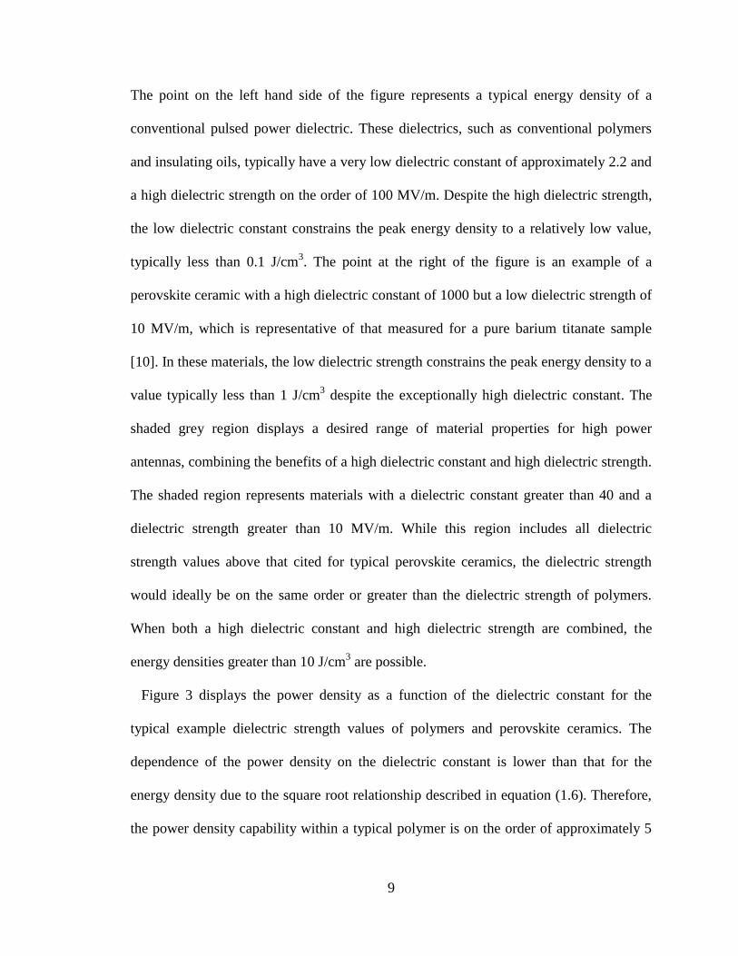
Figure 2 shows a plot of the peak energy density vs. dielectric constant for dielectric
strength values of 10 MV/m and 100 MV/m.
Figure 2. Energy density vs. dielectric constant for dielectric strengths of 10 MV/m and
100 MV/m
9
The point on the left hand side of the figure represents a typical energy density of a
conventional pulsed power dielectric. These dielectrics, such as conventional polymers
and insulating oils, typically have a very low dielectric constant of approximately 2.2 and
a high dielectric strength on the order of 100 MV/m. Despite the high dielectric strength,
the low dielectric constant constrains the peak energy density to a relatively low value,
typically less than 0.1 J/cm3. The point at the right of the figure is an example of a
perovskite ceramic with a high dielectric constant of 1000 but a low dielectric strength of
10 MV/m, which is representative of that measured for a pure barium titanate sample
[10]. In these materials, the low dielectric strength constrains the peak energy density to a
value typically less than 1 J/cm3 despite the exceptionally high dielectric constant. The
shaded grey region displays a desired range of material properties for high power
antennas, combining the benefits of a high dielectric constant and high dielectric strength.
The shaded region represents materials with a dielectric constant greater than 40 and a
dielectric strength greater than 10 MV/m. While this region includes all dielectric
strength values above that cited for typical perovskite ceramics, the dielectric strength
would ideally be on the same order or greater than the dielectric strength of polymers.
When both a high dielectric constant and high dielectric strength are combined, the
energy densities greater than 10 J/cm3 are possible.
Figure 3 displays the power density as a function of the dielectric constant for the
typical example dielectric strength values of polymers and perovskite ceramics. The
dependence of the power density on the dielectric constant is lower than that for the
energy density due to the square root relationship described in equation (1.6). Therefore,
the power density capability within a typical polymer is on the order of approximately 5

10
GW/cm2, and the power density calculated for a typical perovskite ceramic is less than 1
GW/cm2. By increasing both the dielectric constant and the dielectric strength in the
composite material, the power density within the composite would be on the order of 10
GW/cm2 to greater than 100 GW/cm
2. The parameter space of desired material operation,
corresponding to a dielectric constant greater than 40 and dielectric strength greater than
that of a ceramic at 10 MV/m, is shaded grey in Figure 3. The desired dielectric strength
is ideally on the same order of magnitude or greater than that observed for polymers,
resulting in power densities greater than 10 GW/cm2.
Figure 3. Power density as a function of the dielectric constant for dielectric strengths of
10 MV/m and 100 MV/m
To ensure the material’s suitability for implementation in high power antennas and other
high voltage components, additional constraints included that the material must be
capable of being formed in thicknesses adequate for very high voltage systems, be

11
machinable to complex geometries, and be manufactured at temperatures much lower
than the sintering temperatures used for perovskite ceramics. Conventional materials
meeting the previously described requirements for dielectric loading of a high power
antenna were unavailable. Therefore, a research effort was necessary to develop a
material combining the benefits of a high dielectric constant with a high dielectric
strength while also meeting the requirements for size, machinability, and manufacturing
conditions.
1.2 Research Goals
The goals of this research include the development of composite materials, dielectric
characterization of the composite materials, design, construction, and low power testing
of a compact antenna incorporating the composite materials, and development of a high
power antenna driver for the dielectric-loaded antenna. These four areas are summarized
in the following itemized goals:
1. Develop high dielectric constant composite materials with the following minimum
specifications:
1.1 Dielectric constant of greater than 40 at frequencies in the VHF and UHF
bands
1.2 Dielectric loss below 0.1 at the frequencies of antenna operation
1.3 Pulsed dielectric strength of greater than 100 MV/m
1.4 Negligible ferroelectric saturation – linear polarization vs. electric field
1.5 Peak energy density of greater than 1 J/cm3
1.6 Capability of being formed into thicknesses greater than 0.5 cm
1.7 Machinability with power and hand tools

12
2. Characterize the dielectric properties of the composite materials with the following
methods:
2.1 Dielectric spectroscopy
2.2 Polarization
2.3 High voltage capacitive discharge
2.4 Pulsed dielectric strength
2.5 Thermogravimetric analysis
2.6 Scanning electron microscopy
2.7 3D Electrostatic Simulation
3. Develop a dielectric-loaded compact antenna according to the following minimum
specifications:
3.1 Operating frequency in the VHF and/or UHF bands
3.2 Demonstration of antenna size reduction when compared to conventional
antennas operating at similar frequencies
3.3 Unity gain or greater at operating frequencies
3.4 Peak power capability of 1 GW or greater
4. Develop and test a high power antenna driver with the following specifications:
4.1 Driving frequency in the VHF and/or UHF bands at frequencies relevant to
the dielectric-loaded antenna
4.2 High peak power operation

13
1.3 Overview
This dissertation is organized along the four tasks outlined in the previous section.
Chapters 2 and 3 detail the development of the high dielectric constant composites.
Chapter 2 examines the theoretical issues critical to the development of high dielectric
constant composites. The range of topics included in Chapter 2 include: a description of
the origin of energy storage in dielectric materials; a discussion and analysis of
mathematical models describing how the dielectric constant of each material within the
composite contributes to the effective dielectric constant of the composite; an analysis of
particle packing and how the volume fraction of a component of the composite can be
maximized; a discussion on how to improve homogeneity throughout the composite; and
lastly how to improve the dielectric strength of the composite. Chapter 3 begins with a
brief review of previous notable works in the field of high dielectric constant composites
to establish a frame of reference for the current work. The chapter then applies the
concepts established in Chapter 2 to discuss the selection of materials, the design of the
distribution of the composites’ elements, and description of the novel manufacturing
methods developed in the course of this work. The three classes of composites developed
in this effort, MU45, MU100, and MU550, are briefly described based on their materials
and manufacturing concepts.
Chapter 4 includes a full description of the methods and results of the dielectric
characterization performed on MU45, MU100, and MU550. The first three
characterization methods listed in goal 2 of the previous section, dielectric spectroscopy,
polarization, and high voltage capacitive discharge, are complementary methods of
determining the dielectric constant and losses under low and high electric field
14
conditions. Dielectric spectroscopy includes the industry-standard method of network
analysis based measurements of the complex permittivity at the frequencies of interest for
antenna operation. Since the high dielectric constant composites are intended for high
power operation, polarization and high voltage capacitive discharge measurements
supplement the low voltage network analysis measurement to account for high electric
field effects. Characterization of the dielectric strength is conducted under pulsed
conditions to replicate the fast dV/dt of the high frequencies of intended operation. The
custom pulsed dielectric test stand is described along with a statistical analysis of
dielectric strength measurements on all three composite classes.
Chapter 5 discusses the development and testing of a high power dielectric resonator
antenna incorporating one of the high dielectric constant composites. A description of
dielectric resonator antennas is provided along with a discussion of coupling methods. An
analysis of the resonant modes is provided with models of the resonant frequency based
on the properties of the high dielectric constant composites. Due to the narrow bandwidth
of many high-Q dielectric resonator antennas, methods to increase the bandwidth are
reviewed. The design and construction of a high power dielectric resonator antenna is
described, and the results of simulations in CST Microwave Studio are analyzed. Finally,
the low power characterization of the antenna is described with results for the return loss
and gain.
Chapter 6 covers the design, construction, and testing of a high power antenna driver
developed to enable antenna testing at high peak power in transient RF bursts. The high
power antenna driver is based on a simulator of a flux compression generator, and a new
design for such a simulator is described. The chapter further describes the use of an

15
exploding wire fuse to interrupt the current in an inductive energy storage system,
charging a high power oscillator and the antenna under test to high voltage. The high
power damped sinusoid oscillations resulting from discharge of the high power oscillator
and antenna provide a high power, high frequency signal that can be radiated by the
antenna. This system is described, and results of initial testing of the high power antenna
driver are presented.
Chapter 7 provides a summary of the most important results of this work. The outcome
of this research is evaluated against the goals established in this chapter. Finally,
suggestions for future work are presented in the areas of material development, material
characterization, modification of the dielectric-loaded antenna, and high power
evaluation of the antenna.

16
References for Chapter 1
[1] C. Balanis, Antenna Theory: Analysis and Design, 3rd ed. Hoboken, NJ: John
Wiley and Sons, 2005.
[2] G. Breed, "Basic principles of electrically small antennas," in High Frequency
Electronics: Summit Technical Media, LLC, 2007, pp. 50-503.
[3] H. Naghib-zadeh, C. Glitsky, I. Dorfel, and T. Rabe, "Low temperature sintering of
barium titanate ceramics assisted by addition of lithium fluoride-containing
sintering additives," Journal of the European Chemical Society, vol. 30, pp. 81-86,
2010.
[4] D. R. Smith, J. B. Pendry, and M. C. K. Wiltshire, "Metamaterials and negative
refractive index," Science, vol. 305, pp. 788-792, 2004.
[5] N. Engheta, "Circuits with light at nanoscales: optical circuits inspried by
metamaterials," Science, vol. 317, pp. 1698-1702, 2007.
[6] A. Salandrino and N. Engheta, "Far-field subdiffraction optical microscopy using
metamaterial crystals: theory and simulations," Physical Review B, vol. 74, 075103,
2006.
[7] S. Enoch, G. Tayeb, P. Sabouroux, N. Guerin, and P. Vincent, "A metamaterial for
directive emission," Physical Review Letters, vol. 89, pp. 213902-1 - 213902-4,
2002.
[8] R. W. Ziolkowski, P. Jin, J. A. Nielsen, M. H. Tanielian, and C. L. Holloway,
"Experimental verification of Z antennas at UHF frequencies," IEEE Antennas and
Wireless Propagation Letters, vol. 8, pp. 1329-1333, 2009.
[9] C. Balanis, Advanced Engineering Electromagnetics. Hoboken, NJ: John Wiley &
Sons, Inc., 1989.
[10] S. Panteny, C. R. Bowen, and R. Stevens, "Characterization of barium titanate-
silver composites Part II: Electrical characteristics," Journal of Materials Science,
vol. 41, pp. 3845-3851, 2006.

17
Chapter 2: Critical Issues in the Development of Composite
Materials Combining High Dielectric Constant and High
Dielectric Strength
2.1 Complex Permittivity and the Dielectric Constant
Throughout this work, the terms permittivity and dielectric constant refer to the primary
parameter of interest in the composite development. Thus it is important to understand
the theoretical basis of this material property and the meaning of these terms. The term
dielectric constant generally refers to the real part of the complex permittivity normalized
by the permittivity of free space. As will be described, the term dielectric constant is
somewhat misleading due to its dependence on a variety of factors, including frequency,
temperature, and electric field. Nevertheless, the term dielectric constant is a commonly
accepted label used throughout the technical literature, so it is the preferred term used in
this work. The following material covers the well-established theory of dielectric
materials, and the majority of the remainder of this section is adapted from parts of
Balanis’ discussion of permittivity [1].
Charges exist in all materials due to the positive charge carried by protons and the
negative charge carried by electrons. Separation of charges within a material can occur on
a variety of scales, including ions or molecules with a net charge, dipoles in which charge
is shared unequally within a molecule or a lattice structure, and dipoles at the atomic
scale where the electron cloud can be unsymmetrical with respect to the nucleus. In a
perfect dielectric material, these charges or dipoles are completely bound, preventing
conduction of current when a constant electric field is applied. The application of a
constant electric field, [V/m], can, however, induce alignment of the dipoles with the

18
electric field, resulting in a net polarization, [C/m2], of the material. As denoted, the
electric field and polarization are vectors. To quantify the polarization with respect to
individual dipoles, the average dipole moment within the material is defined as the
product of the charge being separated in each dipole, q [C], and the average distance the
charges in the dipole are separated, [m] [1]. This average distance is also a vector in
the same direction as the polarization and electric field. The polarization can then be
defined based on the number of dipoles per unit volume, N [m-3
] [1].
(2.1)
The polarization can be a result of charge separation due to any or all of the mechanisms
previously discussed. Even in the absence of a dielectric material, energy can be stored in
an electric field in vacuum. The constitutive relation of the electric flux density, [C/m2]
to the electric field in a vacuum is given by equation (2.2) [1]. The term ε0 [F/m]
represents the fundamental physical constant referred to as the permittivity of free space.
(2.2)
When a dielectric material is present in the electric field, the polarization as calculated in
equation (2.1) is additive to the electric flux density of vacuum as described by equation
(2.2).
(2.3)
If a static permittivity is defined as εs [F/m], equation (2.2) can be rewritten as equation
(2.4) [1].
(2.4)
Since is a function of the electric field, the polarization is also a function of the
electric field based on equation (2.1). Thus it is possible to define the polarization with

19
respect to the electric field and the permittivity of free space as equation (2.5). To permit
this equality, the dimensionless quantity χ is defined as the electric susceptibility [1].
(2.5)
The electric flux density can be rewritten based on this new definition of the polarization
as equation (2.6) [1].
(2.6)
By equating equation (2.6) with equation (2.4), the static permittivity can be defined as
equation (2.7) [1].
(2.7)
If the static permittivity is normalized by the permittivity of free space, a new value can
be defined that is the relative static permittivity [1]. Since the relative static permittivity
is defined relative to the permittivity of free space, it is a dimensionless quantity. This
value is the dielectric constant in a static field. However, even in this case of a static field,
the term dielectric constant is somewhat misleading based on the common dependence of
the value on factors such as temperature and field strength.
(2.8)
The preceding discussion can be extended to the case of alternating electric fields by
recognizing that under the influence of an alternative electric field, of equation (2.1)
becomes a function of time. Thus the separation of charges oscillates with the electric
field. The oscillating charges experience both an attractive force pulling the opposite
charges together and a damping effect opposing the motion of the charges. This is similar
to the mechanical situation in which a mass attached to a spring oscillates with a damping
factor due to friction [1]. From an analysis of this oscillating system, the distance

20
between charges as a function of time, l*(t) [m], due to an oscillating electric field, E(t)
[V/m], can be written as equation (2.9) [1]. The symbol d represents the damping
coefficient, and the symbol m [kg] is the effective mass of the charge. The symbol ω
[rad/s] is the angular frequency, and the resonant angular frequency of the system is
represented as ω0 [rad/s]. The imaginary unit is represented as i. A superscript asterisk is
added to symbolize all quantities that are complex.
(2.9)
From equations (2.9), equation (2.1) can be expanded to the time-varying case as
equation (2.10) [1].
(2.10)
Applying the same logic used to define the static permittivity through equations (2.4),
(2.6), and (2.7), the time-varying permittivity can be determined as equation (2.11) [1].
The permittivity has both real and imaginary parts, so it is now referred to as the complex
permittivity [1].
(2.11)
Normalizing equation (2.11) by the permittivity of free space provides the complex
relative permittivity [1].
(2.12)
The complex relative permittivity is often discussed in the context of its real and
imaginary parts.

21
(2.13)
The real and imaginary components of the complex relative permittivity can be separated
from equation (2.12) as equations (2.14) and (2.15) [1].
(2.14)
(2.15)
The preceding equations explain the physical origin of the complex relative permittivity
and its real and imaginary components. To understand how the quantities of equation
(2.14) and (2.15) translate to energy storage and loss, the derivative form of the Maxwell-
Ampere equation, which includes the complex permittivity, can be considered [1]. The
symbol [A/m] represents the magnetic field, and the symbols [A/m2] and [A/m
2]
represent the impressed and conduction current densities, respectively. It should be noted
that the permittivity values in equation (2.16) and subsequent equations have not been
normalized by the permittivity of free space, so they are equal to the product of ε0 and the
relative values given by equations (2.14) and (2.15).
(2.16)
The conduction current density can be calculated as the product of the static conductivity,
σs [Ω-1
] and the electric field. Applying this relation and simplifying equation (2.16)
produces equation (2.17) [1].
(2.17)

22
As seen in equation (2.17), the imaginary component of the complex permittivity
contributes to a real component of the current density, and the real component of the
complex permittivity forms the imaginary component of the current density. Further
combination of terms in equation (2.17) derives equation (2.18).
(2.18)
In the format of equation (2.18), the loss tangent, , is present, as defined by equation
(2.19) [1].
(2.19)
In most good dielectrics, the static conductivity can be neglected. In that case, the loss
tangent is simplified to equation (2.20). Since both ε” and ε’ include the permittivity of
free space, the loss tangent can also be written in terms of the ratio of the relative
complex permittivity values. The loss tangent is also equivalent to the dissipation factor.
(2.20)
Throughout this text, the terms dielectric constant or relative permittivity will be used to
refer to the real component of the complex relative permittivity, represented as εr’ or
simply εr. This term is used due to its accepted usage in the technical literature with
acknowledgement that the dielectric constant is not constant but rather is a function of
frequency, temperature, electric field and other factors. The terms loss tangent or
dissipation factor, as well as a general reference to dielectric losses, are used to refer to
the losses as a result of time-varying electric fields. When appropriate, losses due to non-
negligible conductivity σs are referred to separately.
23
As shown in equations (2.14) and (2.15), the real and imaginary components of the
complex relative permittivity have a resonant frequency, ω0, around which the complex
permittivity undergoes a significant transition. As the polarization of a material can be the
result of the multiple polarization mechanisms previously discussed, the material may
have multiple resonant frequencies. Figure 4 illustrates the general behavior of the real
and imaginary components of the complex permittivity with respect to frequency for the
various polarization mechanisms. At the resonant frequency for a particular polarization
mechanism, there is significant dispersion in the real part of the complex permittivity,
and the imaginary component reaches a maximum. Thus, it is generally disadvantageous
to operate a dielectric material near the resonant frequency of the polarization mechanism
as it corresponds to a dispersion in the dielectric constant and high dielectric losses. This
presents a challenge in this work due to the frequency range of interest for antenna
operation in the VHF and UHF bands. In these bands, many materials exhibiting dipolar
polarization have high dispersion of the dielectric constant and high dielectric losses.
This factor limits the use of highly polar polymers as effective binders as the high
dielectric constant of these polymers is much lower in the VHF and UHF bands and the
dielectric losses are high.

24
Figure 4. The complex permittivity as a function of frequency showing general trends
due to the ionic, dipolar, atomic, and electronic polarization mechanisms. Illustration
used under open license [2].
In addition to providing a derivation of the dielectric constant and dielectric losses, the
preceding discussion also gives insight to begin the discussion on how a high dielectric
constant material can be developed. As described by equation (2.11), increasing the
dielectric constant arises from increasing the polarization for a given electric field. The
factors determining the polarization apply directly to calculation of the dielectric constant
in equation (2.14). Specifically, by increasing the number of dipoles per unit volume, N,
and/or the quantity of charge being separated in each dipole, q, the dielectric constant is
increased. While the dielectric constant of a given material can be designed and
controlled to a certain extent by controlling these parameters, it is not the object of this
work to control these parameters in the design of a new material. Rather, the object of
this work is to create composites composed of two or more materials which collectively

25
exhibit the desired properties of high dielectric constant and high dielectric strength. In
the process of combining multiple materials into a new composite material, the effective
properties of the composite are determined as a weighted average of the properties of the
components of the composite. Thus, to develop a high dielectric constant composite
material, it is necessary to retain a high average number of dipoles per unit volume, Nav,
and a high average charge per dipole, qav. The next section discusses models used to
calculate the effective dielectric constant of a composite material based on a weighted
averaging process of the amount and properties of the composite’s component materials.
2.2 The Effective Dielectric Constant of Composites
2.2.1 Background on the Effective Dielectric Constant
Since the high dielectric constant material is developed as a composite, it is by
definition composed of more than one material. Since the materials that constitute the
composite often have very different physical properties, including electrical properties,
prediction and modeling of the effective properties of the composite is dependent on
several factors. These factors include the proportions of the individual materials forming
the composite, the physical properties of each material, and the coordination of the
various materials after being mixed and packed. The multitude of possible combinations
of materials and composite arrangements results in a nearly limitless number of potential
composite properties, which can make predictive modeling very difficult. However, by
limiting the scope of properties of interest to the relative permittivity, it is possible to
obtain an approximation that is helpful in designing composites according to the desired
specifications.

26
In high dielectric constant polymer-ceramic composites, the energy storage capabilities
of these two main classes of constituent materials are typically very different. Polymers
often exhibit excellent dielectric strength, but the dielectric constant is often very low,
typically less than 5. Some relatively new classes of polymers exhibit higher dielectric
constants, but they are generally only effective at lower frequencies than the VHF and
UHF range of interest. Conversely, perovskite ceramic materials, as will be discussed in
later sections, are capable of storing very high amounts of electrostatic energy at reduced
electric field strengths. These ceramics can have dielectric constants of several hundred
to many thousand, depending on the temperature of the material and the frequency of the
applied electric fields. Mixing these two very different classes of materials creates a
composite with an effective dielectric constant between the two extreme values. Several
equations exist to predict the effective dielectric constant of composite systems. To
compare the accuracy of the models without the influence of experimental error, a
software program was developed to build and simulate three-dimensional dielectric
composites.
2.2.2 Mathematical Models
One of the most commonly implemented equations for predicting the effective
dielectric constant of dielectric composites is Lichtenecker’s logarithmic mixing rule, as
given by equation (2.21). Lichtenecker’s rule is unique in that it can be applied for an
unlimited number of components. It determines the effective dielectric constant of the
composite based on the dielectric constant of each component, εi, weighted by the volume
fraction of the composite that each component occupies, vi. The effective dielectric
constant of the composite is represented as εeff. As presented in equation (2.21), the

27
logarithmic terms have a base of ten. The natural logarithm or any other base to the
logarithms can be used as long as use of the chosen base is consistent throughout the
equation.
(2.21)
Equation (2.22) provides the expanded form of equation (2.21) for a three-component
composite consisting of ceramic, polymer, and voids. In this example, the subscript c
denotes that the corresponding dielectric constant or volume fraction value is for the
ceramic content of the composite. Similarly, the subscript p represents the polymer
contents, and the subscript void denotes the values for the voids within the composite.
(2.22)
Lichtenecker’s rule has historically been used extensively due to its correlation with
experimental data without a firm theoretical base for its application. However, a recent
study derived Lichtenecker’s rule from Maxwell’s equations based upon conservation of
charge for composites with randomly shaped and oriented constituents [3].
There are several other models developed specifically for determining the effective
dielectric constant of composites, and the following examples should not be considered
an exhaustive list. The following formulas are presented as given in a short review of
equations developed for the effective dielectric constant [4]. As will be seen, all of the
following models were developed for two-component composites. Unlike the
Lichtenecker equation, these models can only account for ceramic and void content, and
the common third component consisting of voids is neglected. Following a previously
defined variable definition, ε represents the dielectric constant of a particular element,

28
with the subscripts p, c, and eff indicating that the dielectric constant corresponds to the
polymer, ceramic, and effective composite values, respectively [4]. Similarly the symbol
v represents the volume fraction of each element as a part of the total composite volume,
and the subscripts p and c denote that the volume fraction corresponds to the polymer and
ceramic components, respectively. Each of the equations is presented in the following
paragraph for reference to the analysis in the next subsection.
Equation (2.23), the Maxwell-Wagner equation, calculates the effective dielectric
constant for a two-phase composite, consisting of one ceramic element and one
polymeric element.
(2.23)
Equation (2.24) is the Yamada equation for a polymer-ceramic composite [4, 5]. The
variable definitions follow the convention used in the Maxwell-Wagner equation. The
variable n is a morphology factor that varies from 0 in the case of all particle connections
in parallel to 1 for the case of all connections in series [4].
(2.24)
Finally, the Jayasundere and Smith equation is shown as equation (2.25) [6]. The
variables follow the previously-defined convention. The Jayasundere and Smith equation
was developed by modifying the Kerner equation to account for interactions between
neighboring polarized spheres.

29
(2.25)
Each of these numerical models has been effective in matching the results of specific
experimental data. However, variations in the experimental conditions of composite
formation and in the minute factors that affect dielectric constant measurements can make
comparison of experimental data to numerical models of the effective dielectric constant
difficult. Therefore, the implementation of a computer simulation in which all of the
factors of composite formation and measurement can be controlled is seen as the
advantageous method for comparing numerical models.
2.2.3 Three-Dimensional Electrostatic Modeling
In parallel with the experimental development of high dielectric constant composite
materials, a computational effort has been conducted to electrostatically model
composites in three dimensions. Due to the many variables that can be adjusted in the
development of composite systems, computer models of composites provide a relatively
fast method for analysis of the effects of individual variables. In addition to reducing the
time needed to predict the properties of a new composite, electrostatic modeling enables
the comparison of composites without the effects of experimental or measurement error.
Since the accuracy of simulation results can only be as good as the modeling method
implemented, the computational and experimental approaches were used in a
complementary effort.
A series of simulations were performed to compare the simulated value of the effective
dielectric constant with the values calculated from the previously detailed equations. The

30
virtual composite geometry and constituent material properties were consistent across all
simulations. The composite form was defined to be a cylinder with a diameter of 10 µm
and a thickness of 5 µm. The filler and void particles were spheres with a radius of 500
nm, so the spherical particles were small enough with respect to the composite form to be
able to be randomly placed throughout the volume. Dielectric constants of 1, 1000, and 5
were used for the voids, filler, and matrix materials, respectively. These values were
chosen to represent air voids, fillers of a perovskite ceramic, and a polar polymer.
In the first simulations, the volume percentage of the filler was varied from 5 to 50% in
steps of 5%. Simulations at volume percentages greater than 50% were not possible due
to the packing density limitations of randomly packed spheres. The binder properties
were kept constant in each simulation, and no voids were initially included. The
simulated data are plotted as points in Figure 5. The curves were plotted by applying
equation (2.21) and equations (2.23)-(2.25), including the actual volume data returned for
each component after the composite was constructed.

31
Figure 5. Effective dielectric constant for variable percentage filler and matrix dielectric
constant
From Figure 5, it is apparent that the Lichtenecker model closely tracks the simulated
data. The Yamada morphology factor of equation (2.23) was selected to match the
simulated data as best as possible. The morphology factor used in the Yamada plot of
Figure 5 was 0.075. The Jayasundere and Smith model underestimates the effective
dielectric constant at all points, and the Maxwell-Wagner equation provides the worst fit
for the simulated data. The accuracy of each model is plotted in Figure 6 as the
percentage difference of the effective dielectric constant from the simulated data. The
Maxwell-Wagner underestimates the simulated data by nearly 70% at high filler loading
levels. The Lichtenecker model, however, remains within ± 8% through the entire range.

32
Figure 6. Percentage difference of the simulated effective dielectric constant from
calculated values
In general, all of the models except the Lichtenecker model would underestimate the
effective dielectric constant from that obtained through simulation. Although the Yamada
morphology factor was chosen such that it matches the simulated results near 5% and
50% and overestimates in other areas, a more appropriate morphology factor of 0.5,
representing the combination of series and parallel particle connectivity of randomly
placed fillers, would also greatly underestimate the simulated results. Some previous
experimental studies have found agreement between measured data and the models that
do not match the simulated results. One potential explanation for this mismatch between
experimental data and the models is the influence of voids, which are unaccounted for in
most models. In real polymer-ceramic composites, voids are nearly impossible to
completely eliminate. Voids can also be difficult to measure directly, so their presence
and significance are often overlooked. Another set of simulations was conducted to
demonstrate the effect of voids on the effective dielectric constant of a composite with a

33
low filler loading. The composite again consisted of a matrix material with a dielectric
constant of 5, 500 nm filler particles with a dielectric constant of 1,000, and 500 nm void
particles with a dielectric constant of 1. The virtual composite had a thickness of 5 µm
and a diameter of 10 µm. The simulation runs varied the volume percentage of voids
displacing the matrix material from 0% to nearly 30%. Due to the upper volume limit on
the total filler and void content, the volume percentage of fillers with a dielectric constant
of 1,000 was kept at 10% in each simulation.
The data were plotted as the percent change in the effective dielectric constant when
compared with the baseline case with 0% voids in Figure 7. The absolute value of the
percentage change steadily increases with increasing voids to the point that the effective
dielectric constant was decreased by more than 20% through the addition of 28.7% by
volume voids. The reduction of the effective dielectric constant is just one of the negative
effects of voids, along with increasing the potential for dielectric failure due to insulation
breakdown.
Figure 7. Percentage change in the effective dielectric constant between a composite
with and without voids

34
2.3 Particle Packing Density
As described by Lichtenecker’s Rule, the effective dielectric constant of a composite
material is equal to the weighted sum of the logarithm of the dielectric constants of each
constituent material of the composite [3]. The logarithmic terms are weighted by the
volume fraction of the composite occupied by that particular material. Therefore, to
maximize the effective dielectric constant of the composite, the material with the highest
dielectric constant must occupy the largest possible volume fraction within the
composite. Perovskite ceramics are the materials with the highest dielectric constant
included in the composite, so the fractional volume of the ceramics must be maximized to
obtain the highest effective dielectric constant possible.
The question of how to most tightly pack a number of solids in a given volume has
been studied in many theoretical and experimental contexts. Considering the packing of
spheres of equal size in a given volume, it has been shown that the greatest density
possible through regular packing of spheres is approximately 74.05% [7]. For irregular
packing, meaning the compression of spheres added randomly to a given volume, it has
been shown that the densest packing of equally-sized spheres is approximately 64% [7].
Since irregular packing best describes the methods by which a composite can be
realistically formed, the maximum density that could be achieved with a single size of
ceramic spherical particles is 64%. However, the density can be increased further both by
the realistic fact that the actual ceramic particles are irregular in shape and through the
use of multiple sizes of particles.
The problem of obtaining the maximum density for multiple discrete particle sizes was
analyzed mathematically by Furnas in publications from 1929 and 1931 with an

35
accompanying experimental investigation by Anderegg [8-10]. Most of the following
concepts and discussion in this section are based on the analyses presented by Furnas [8,
9]. Some equations have been restructured to solve for the parameters of greatest interest
for application in the composites. The issue of mixing multiple particle sizes together to
form a final mixture with higher density than any of the individual components alone will
first be approached for the bimodal case. In the following definitions and equations, the
subscript x is used as any positive number corresponding to a given set of particles. The
subscript can only apply to one set of particles for any one equation. By definition, the
particle set denoted 1 is the largest particle size, corresponding to a particle dimension d1
[m], and successively smaller particles are denoted by increasing numbers. Furnas
defines particles to be the same size if they cannot be separated through screens differing
by a factor of [9].
A set of particles of a given size is defined to have a common material density, ρMx
[kg/m3]. The material density is the actual density of the material as opposed to the
density of multiple packed particles. When the particles are packed into a container, a
fraction, vx, of the total volume of the bed of particles, VTx [m3], remains unfilled by
particles. Throughout this discussion, reference to a volume fraction of voids refers to the
voids within a bed of packed particles. The individual particles themselves are considered
fully dense with a density equal to the material density. The lowercase letter v denotes
void fractions whereas the capital letter V denotes volumes. The total volume of the bed
is partially filled by the particles and partially left unfilled by spaces considered voids. If
a mass of particles, mx [kg], is packed into a container, several relationships can be
mathematically defined. First, the volume occupied by the particles themselves, which is

36
a distinct quantity from the volume filled by the particles and voids, can be defined as Vx
[m3].
(2.26)
The void fraction, vx, is then defined using equation (2.27).
(2.27)
Due to the volume occupied by the voids, the apparent density of the bed of particles will
be less than the material density. The apparent density or bulk density, ρBx [kg/m3], of the
bed of particles can thus be defined using equation (2.28).
(2.28)
The material density and bulk density can be related through the void fraction.
(2.29)
Consider a bed of packed particles with dimension d1 [m], material density ρM1 [kg/m3],
and void fraction v1 filling a total volume VT1 [m3] as previously defined. If a second,
much smaller set of particles with dimension d2 [m], material density ρM2 [kg/m3], and
void fraction v2 is added to the first bed of particles, the density of the mixture can often
be increased, resulting in a smaller void fraction for the mixture. Ideally, the second set of
particles would be infinitely small such that they completely fill the voids of the first set
of particles. In all real systems, the particles constituting the second set will have finite
dimensions, and the packing of the second set of particles will also contain voids. Figure
8 is a simplified illustration of the previously described cases of a bed of large particles
and the large bed filled with ideal and realistic smaller particles.
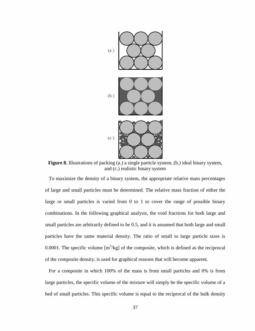
37
Figure 8. Illustrations of packing (a.) a single particle system, (b.) ideal binary system,
and (c.) realistic binary system
To maximize the density of a binary system, the appropriate relative mass percentages
of large and small particles must be determined. The relative mass fraction of either the
large or small particles is varied from 0 to 1 to cover the range of possible binary
combinations. In the following graphical analysis, the void fractions for both large and
small particles are arbitrarily defined to be 0.5, and it is assumed that both large and small
particles have the same material density. The ratio of small to large particle sizes is
0.0001. The specific volume [m3/kg] of the composite, which is defined as the reciprocal
of the composite density, is used for graphical reasons that will become apparent.
For a composite in which 100% of the mass is from small particles and 0% is from
large particles, the specific volume of the mixture will simply be the specific volume of a
bed of small particles. This specific volume is equal to the reciprocal of the bulk density

38
of the small particles and is labeled point 1 on the ordinate of Figure 9. Similarly, if the
composite were composed of 100% large particles and 0% small particles, the specific
volume of the mixture would be the equal to the reciprocal of the bulk density of the
large particles. The specific volume corresponding to 100% large particles is labeled
point 3 in Figure 9. Considering a system defined by point 3, if infinitely small particles
were gradually added to the voids of the large particles, the total mass of the system
would go up without any increase in the total volume. The specific volume would follow
the solid line from point 3 towards point 2. The density would reach a maximum when
the infinitely small particles had completely filled the voids of the large particles. At this
point, the specific volume of the composite would be equal to the reciprocal of the
material densities of the two sets of particles. This point is represented by point 2 in the
normalized graph of Figure 9. The dependence of the location of point 2 with respect to
the fraction of total mass composed of large particles will be described later. The dotted
line in Figure 9 connecting points 1 and 2 is analogous to the solid line between points 3
and 2. If a bed of small particles has large particles gradually added to it such that the
mass of the system is increased without increasing the system’s volume, the specific
volume will decrease until it reaches the point at which there are no remaining voids and
the specific volume of the composite is equal to the reciprocal of the particles’ material
density. Whereas the lines between points 1 and 2 and points 2 and 3 represent the
idealized case in which the small particles are infinitely smaller than the large particles,
the line between points 1 and 3 represents the worst-case scenario in which the small
particles are equal in size to the large particles. In this case, since the material and bulk
densities of the composites are the same, the addition of particles from one set to a

39
system composed exclusively of particles from the other set would not alter the specific
volume. As mathematically described later, the line between points 1 and 3 is not
necessarily parallel to the abscissa. The shaded triangle formed by points 1, 2, and 3 in
Figure 9 represents the range of composite densities possible with this binary system.
Figure 9. Possible normalized densities in a binary system with 50% voids in a bed of
each component
The ideal minimum specific volume represented by point 2 cannot be reached in a real
system because any real set of small particles will have finite size and be unable to
completely fill the voids of a larger set of particles. However, the fraction of the total
mass for each component in an ideal system of maximum density is still very useful to
design a real system with an optimized density. To determine the proportions of each
component at ideal maximum density, the equations representing the solid and dotted
lines of Figure 9 can be used. The mass of the large and small components are defined to
40
be m1 [kg] and m2 [kg], respectively. The fraction of the total weight contributed by the
large component can then be defined as Z1 with equation (2.30) [9].
(2.30)
The line represented as SV1 [m3/kg] in Figure 9 can be written mathematically based on
its previous description. Starting with a composite of 100% small particles, large particles
are added such that the volume of the composite does not increase. This describes a line
between the reciprocal of the bulk density of the small particles and the reciprocal of the
material density of the large particles, as shown in equation (2.31) [8].
(2.31)
Equation (2.31) represents an ideal composite and a lower limit of possible specific
volume values for low values of Z1. However, at some point the line crosses into a region
in which it describes a purely theoretical composite. For 100% large particles, SV1
predicts a composite specific volume equal to the specific volume of the material without
any voids. Since it is known that a bed of all large particles contains voids, this point on
SV1 is impossible to achieve even in an ideal system. Therefore, SV2 [m3/kg] is necessary
to establish a lower limit of possible specific volume values for relatively high values of
Z1. This lower limit can be drawn as a straight line from the origin to the specific volume
at 100% large particles [8]. The line represented as SV2 can be described by equation
(2.32) [8].
(2.32)
41
Lines SV1 and SV2 are the two lower limits for the range of possible specific volume
values. The point of maximum density of the ideal system, represented as point 2, can be
determined as the intersection of the two lines, as shown in equation (2.33) [8].
(2.33)
Equation (2.32) can be solved for the value of Z1 that creates the ideal composite of
maximum density, and the result is given as equation (2.34).
(2.34)
The upper limit of possible specific volume values, represented as the line between points
1 and 3 in Figure 9, can be determined mathematically as a straight line connecting the
reciprocals of the bulk densities of the small and large particles. The upper limit, denoted
SV3 [m3/kg], can be expressed as equation (2.35). The upper limit is not parallel with the
abscissa if the material densities or void fractions of the large and small particles differ
[8].
(2.35)
With the limits of all possible values for the specific volume established through
analysis of an ideal system in which the ratio of small to large particle dimensions goes to
zero, values for real systems can be determined when considering systems with finite
ratios of small to large particle dimensions. In the ideal system with infinitely larger large
particles than small particles, the voids of the large particles are perfectly filled with
small particles without increasing the volume of the composite. As a result of the finite
ratio between small and large particles, imperfect packing occurs. Not only are voids
present in the filled voids of the large particles, but the volume of the composite can be

42
increased through the addition of small particles. Furnas introduced a factor y that
accounts for the decrease in volume that occurs when two particle sizes are thoroughly
mixed with respect to the volume of each of the particle sizes when unmixed [9]. When
the particle sizes are equal, y is equal to zero, and the composite volume has been
increased by the volume of the bed of small particles. When the smaller particle size is
infinitely small with respect to the large particle size, y is equal to 1, and the volume of
the composite is equal to the volume of the bed of large particles. There is no known
theory to accurately describe how y varies between zero and one, and the variation of y
with respect to the ratio of largest to smallest particle size can be dependent on the
morphology of the particles. Therefore, equations for y are generally determined
experimentally. From experimental data, Furnas obtained equation (2.36) as a curve fit to
data obtained on the degree of compaction upon mixing with respect to the ratio of
particle sizes [8, 9]. The variable n is defined as one less than the total number of particle
sizes included in the composite [9]. For the binary system currently under consideration,
the variable n is simply equal to 1. The degree of compaction, y, is a function of the ratio
of the smallest particle size, dn+1 [m], to the largest particle size, d1 [m].
(2.36)
By analyzing the trend line used by Furnas to obtain equation (2.36) with the aid of
computational curve fitting, a more precise relationship was obtained, as given in
equation (2.37). Additional trend lines have been produced by other researchers for
specific particle morphologies. Those trend lines can be interchanged to calculate the
factor y when the conditions under which they were measured correspond with the
system under design.

43
(2.37)
By including the effects of the ratio of particle sizes on particle packing, it is evident that
the real values of composite specific volume vary from the ideal case of the greater value
from either equation (2.31) or (2.32) to the maximum specific volume of equation (2.35)
by the factor y. Therefore, equations (2.31) and (2.32) can be modified to include the
factor y to predict real values of the composite specific volume. Equation (2.31) for SV1
can be modified to equation (2.38) [8, 9].
(2.38)
When y is equal to 1 as in the ideal situation, equation (2.38) reduces to equation (2.31),
and when y is equal to 0 for a system of equal particle sizes, the equation reduces to
equation (2.35). Equation (2.32) can similarly be modified to equation (2.39) [8, 9].
(2.39)
When y is equal to 1 as in the in the ideal case, equation (2.39) reduces to equation (2.32),
and when y is equal to 0 for a system of equal particle sizes, equation (2.39) reduces to
equation (2.35). Equations (2.38) and (2.39) can be set equal to each other to determine
the value of Z1 for maximum density in systems with non-ideal packing.
(2.40)
In the ideal case in the limit as y approaches 1, equation (2.40) reduces to the ideal
equation for Z1 in presented as equation (2.34). As y is reduced towards the limit of zero,
Z1 approaches the value 0.5. This result is intuitive in that as the difference in particle

44
sizes becomes less and less, each particle size contributes approximately half of the total
weight of the composite. Equation (2.40) is undefined for a y value of zero, but it is
understood that when the particles are exactly the same size, the relative proportions can
be chosen as any possible value.
Implementing equations (2.38) and (2.39), values of the specific volume of practical
systems with finite values of
can be produced for binary systems in any
proportion. Figure 10 shows the theoretical results of the same binary system used to
produce Figure 9 with specific values for the ratio
. For a very small value of
, 0.0001, the lines approach the lines formed in the ideal case. For intermediate
values in which the large particle is only 400%, 200%, or 33% larger than the small
particle, the decrease in specific volume achieved by mixing the two component sizes is
significantly less than that achieved in the ideal case. Additionally, as the size ratio
increases towards 1, the fraction of total weight contributed by the large component tends
towards 0. Therefore, to best improve the composite density through multimodal packing,
it is generally best to have particle sizes differ by an order of magnitude or more.

45
Figure 10. Theoretical specific volume for practical ratios of small to large particle sizes.
A bed of each particle size is assumed to be 50% voids by volume.
For simplicity, Furnas’ analyses of practical systems concentrate on those in which the
void fractions and material densities for the large and small particles are equal [9]. When
the material densities of particles of both sizes are equal, the mass fraction and volume
fraction of a particle size are identical. For these systems, equation (2.34) reduces to
equation (2.41), where v is the common value of the void fractions.
(2.41)
While previous analysis was limited to a bimodal system. However, Furnas has shown
that the analysis can be extended to higher order systems [9]. For a system in which each
of the particle sizes has the same volume fraction of voids, the ratio of successive particle
sizes for maximum density is the same for all successive particle sizes. This relationship
can be mathematically written as equation (2.42) where dx [m] is the dimension of a

46
particular particle size [9]. The largest and smallest particle sizes are selected according
to the limitations of the application, and the intermediate sized particles can be
determined with equation (2.42).
(2.42)
From equation (2.42), the middle particle size, d2, of a trimodal system can be determined
from the large, d1, and small, d3, particle sizes with equation (2.43) [9].
(2.43)
In the preceding bimodal discussion, Z1 represented the mass fraction of the large
particles. Under the assumption that the material density and void fraction of all particle
sizes are the same, the mass fraction is equal to the volume fraction. With this
assumption, the mass fraction and volume fraction of the large particles in the bimodal
case can both be calculated from equation (2.41), and the mass fraction and volume
fraction of the smaller particles is equal to 1-Z1. The mass fractions and volume fractions
of particle sizes beyond the first two components can be calculated when it is
acknowledged that the small particles of a bimodal system will not perfectly fill the voids
of the large particles. Again assuming that all of the particle sizes in the multimodal
system have the same fraction of voids and material density, it can be shown from
Furnas’ discussion that the ratios of successive values of Z1 are the same [9]. This
relationship is shown in equation (2.44). As seen in the right-hand side of equation (2.44),
this ratio can be determined from the previously calculated value for Z1.
(2.44)

47
Using this ratio and the definitions of Z1 and Z2 as described in the previous paragraph,
equation (2.45) can be derived for the mass fraction and volume fraction of any
component, Zx.
(2.45)
Furnas has shown through a geometrical progression that the total absolute volume,
V1:n=1, of all of the particles in the composite can be calculated as equation (2.46) [9].
This volume applied to the particles only and excludes any voids remaining between the
particles. Since this is an absolute volume, it is defined on a per unit volume basis and is
unitless.
(2.46)
The total absolute volume including the volume of the voids can be defined as equation
(2.47) [9]. The symbols ρM [kg/m3] and ρB [kg/m
3] represent the common values of the
true material mass density and apparent bulk density, respectively.
(2.47)
The volume fraction of voids, vvoids, can be determined based on equations (2.46) and
(2.47).
(2.48)
Since the assumption of a common material mass density and volume fraction is
applied to all particle sizes, the absolute volume can also be considered as an absolute
mass term. Therefore, the relative mass or volume of any component can be calculated as
the ratio of the values determined with equations (2.45) and (2.46). When manufacturing

48
a composite, it is easiest to determine the mass of each component size, so equation
(2.49) is used to calculate the mass of any component relative to the total mass of all
particle sizes, mT [kg]. Since Z1 is only a function of v under the assumption of a common
material mass density and void fraction, the masses can be calculated based on the
volume fraction and total number of particle sizes.
(2.49)
While the preceding discussion outlines the theoretical framework for multimodal
particle packing, the following discussion details how a multimodal particle system can
be designed. The first issue examined is whether to implement 2, 3, or 4 particle sizes in
the system. The effects of particle sizes can be graphically analyzed by plotting the
volume fraction of voids based on equation (2.48). Given the variables of equation (2.48),
the volume fraction of voids is ultimately dependent on the volume fraction of voids for
all of the components, the particle size ratio
, and the total number of particle sizes
n+1. Figure 11 shows the volume percentage of voids with respect to the particle size
ratio for binary, ternary, and quaternary systems in which the volume percentage of voids
in each particle size alone is 40%. Similar graphs can be produced for other initial
volume percentages of voids. Figure 11 shows that for a ternary or trimodal particle
system with initial voids of 40% at each particle size, the voids can be reduced to
approximately 10% by volume when the size ratio of largest to smallest voids is
approximately 1,000.
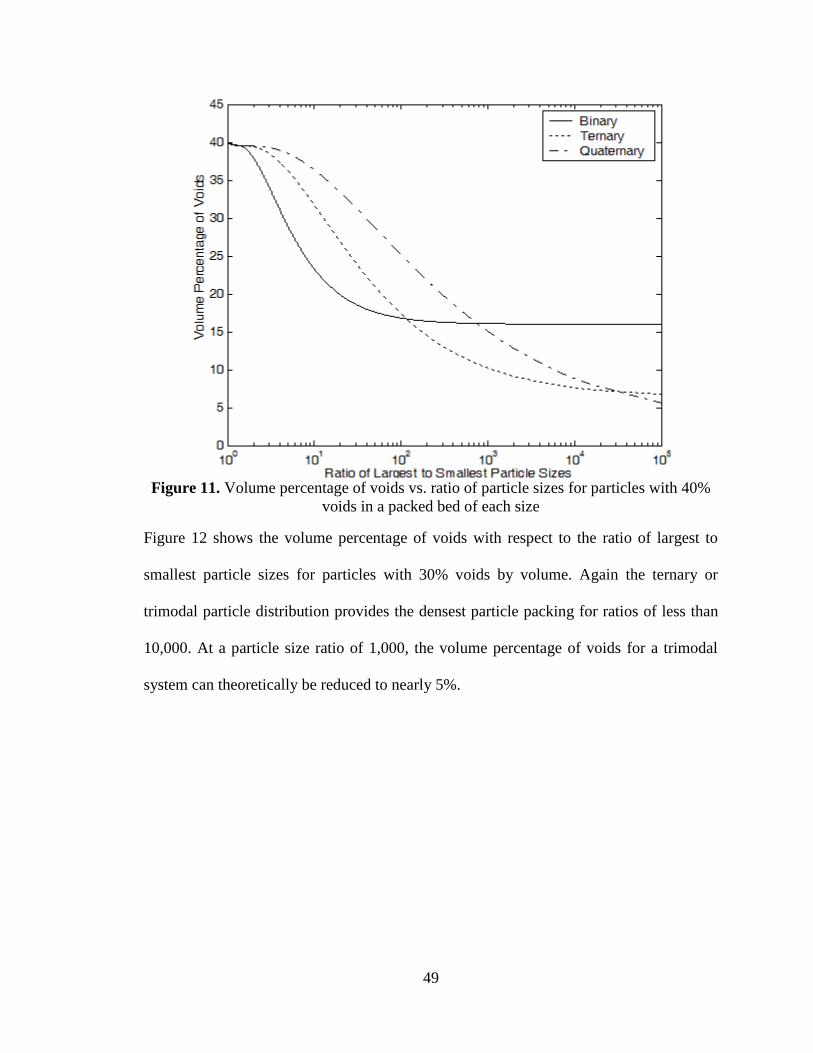
49
Figure 11. Volume percentage of voids vs. ratio of particle sizes for particles with 40%
voids in a packed bed of each size
Figure 12 shows the volume percentage of voids with respect to the ratio of largest to
smallest particle sizes for particles with 30% voids by volume. Again the ternary or
trimodal particle distribution provides the densest particle packing for ratios of less than
10,000. At a particle size ratio of 1,000, the volume percentage of voids for a trimodal
system can theoretically be reduced to nearly 5%.

50
Figure 12. Volume percentage of voids vs. ratio of particle sizes for particles with 30%
voids in a packed bed of each size
From Figure 11 and Figure 12, the ratio of largest to smallest particle sizes was chosen
to be 1,000. The design of this ratio leveraged one of the unique requirements of this
work. Since the composites under development were intended to be produced in
relatively large bulk amounts for incorporation into antennas rather than as very thin
films, larger particle sizes could be included. Extending the size ratio beyond 1,000
becomes impractical, and the rate of reduction of the void content diminishes when
further increasing size ratio.
The lower limit of the smallest particle size is determined by the practical size of
nanoparticles that can be kept from agglomerating and effectively incorporated into the
composite. The desired nanoparticle size was designed to be 50 nm, but any nanoparticles
less than 100 nm would be acceptable. There is little advantage to going to even smaller
nanoparticles, and there is evidence that when perovskite nanoparticles are reduced below

51
a certain level, the lattice structure changes, resulting in a reduction of the nanoparticles’
dielectric constant.
With a small particle size set at 50 nm, the designed size ratio dictates that the largest
particles should be 50 µm. To determine if particles on the order of 50 µm are reasonable,
limitations presented by the dimensions of the composite to be formed and dielectric
strength or the wavelength of the waves propagating through the material must be
considered. For dielectric strength considerations in thin films, a maximum particle size
equal to 1/10th
of the film thickness has been chosen such that dielectric failure in a single
particle does not cause dielectric failure of the entire film. In thick composites, the size of
the largest particles has been limited to a few hundred microns to ensure homogeneity of
the composite, especially for use at high frequency. For the composite to appear
homogenous to an electromagnetic wave propagating through it, the largest particles
should be much smaller than the wavelength of the wave in the material. At the high
frequency end of the bands considered, a 3 GHz signal will have a wavelength in free
space of approximately 0.1 m. From equation (1.4), the wavelength will be decreased
proportionally by the square root of the permittivity. Particle dimensions up to 100 µm
are a factor of ten or more smaller than the wavelength of a wave propagating in a
material with a dielectric constant up to 10,000. Thus, for the range of dielectric constants
and frequencies considered in this work, the restriction on the largest particle size based
on dielectric strength considerations is dominant.
The calculated large particle size on the order of 50 µm was determined to be
reasonable. For composites with a thickness of 1 mm, a single 50 µm particle only
constitutes 5% of the thickness. To maintain homogeneity, a standard was determined

52
that no single particle should be greater than 10% of the composite thickness. As
described in Chapter 4, the manufacturing process of the large particles did not produce a
uniform size of particles but rather a distribution of large particle sizes was obtained.
Large particles ranging from around 40 µm up to 212 µm were often used.
Implementing equation (2.43), the size of the intermediate particles is calculated to be
approximately 1.6 µm. This corresponds to a size ratio of or 31.6 between
particle sizes. The intermediate particles were obtained commercially at a size rated as
less than 3 µm. Although the theoretical analysis concentrated on uniform particle sizes
for simplicity, a distribution of particle sizes can increase the packing density even
further. Thus, the distribution of particle sizes in the large and intermediate sizes was
beneficial to the particle packing density.
To determine the volume percentage of voids in a compacted bed of each of the three
particle sizes, each particle size was pressed into a disk without binder or any other
additive. Although these disks were very fragile, the mass and volume of the disks were
determined to calculate the mass density. With the known density of the ceramic, the
volume percentages of voids and ceramic were calculated. Table 1 summarizes the results
of this experiment. Two sets of large particles were evaluated due to differences in the
source material used to produce them. The volume percentages of voids were 25.97% and
33.48%. While 25.97% is a lower volume percentage of voids than expected, the value is
likely lowered due to the incorporation of smaller particles as a result of the milling
process used to produce the particles. The intermediate size particles and nanoparticles
had volume percentages of voids of between 40% and 45%. All of these values fall
within a useful range for incorporation in a trimodal distribution. The values around 30%

53
and 40% volume of voids fit well with the graphs of Figure 11 and Figure 12, which were
used to determine the particle size ratio.
Table 1. Density of compacted beds and particles and the corresponding volume
percentages of voids and ceramic
Bulk Density
(g/cm3)
Volume Percentage
of Voids
Volume Percentage of
Ceramic
Large Particles 1 4.46 25.97% 74.03%
Large Particles 2 4.00 33.48% 66.52%
Intermediate
Particles 3.54 41.16% 58.84%
Nanoparticles 3.14 44.72% 55.28%
From the preceding analysis and equation (2.49), the mass percentage of each
component was calculated. The calculations assumed that the volume percentage of voids
for each individual particle size was 30%, which corresponds to the value calculated for
the large particles. The weight percentages of the large, intermediate, and small particles
were calculated to be 72%, 21%, and 7%, respectively. This distribution was applied in
the trimodal composites reported in this work.
2.4 Homogeneity
For a composite’s properties to be consistent throughout the material, the proportions of
the constituent materials must be the same in any small volume throughout the
composite, the constituent materials must be evenly dispersed, and the constituents must
be packed to the same density throughout the composite. A composite in which these
conditions are met is considered homogenous, and the composite’s properties are the
same in any small volume throughout the material. Creating a homogenous composite is
required so that the dielectric constant, dielectric strength, and mechanical integrity of the
composite are the same throughout the material. If there are significant variations in the

54
dielectric constant between different regions of the composite, the propagation of
electromagnetic waves through a device formed with the composite may be altered in
such a way that the device’s performance is degraded. This effect could be manifested as
scattering due to discontinuities in the impedance of the composite, causing reflections
and reducing the radiated output of an antenna. If the dielectric strength of the composite
is reduced due to inhomogeneous regions of the composite, the electrically insulating
function of a device formed with the composite could catastrophically fail, causing the
device to be unusable at high voltage. Lastly, if the mechanical integrity is compromised
by inhomogeneous regions, the composite could suffer chipping, flaking, or cracking. For
consistency in these three material properties and several others, the homogeneity of the
composite is critical to its functions.
The first two conditions, requiring equal proportions of the constituent materials and
even dispersion, can both be satisfied through mixing procedures and surface preparation.
For adequate mixing, forces strong enough to break the inter-particle attraction caused by
the high surface area of very small particles must be overcome. In particular, van der
Waals forces between particles can cause attraction between particles that would result in
insufficient mixing. When particles group together due to these small-scale forces,
agglomerates can form that create inhomogeneous regions and degraded composite
properties. Attractive forces between nanoparticles can result in the formation of
agglomerates and aggregates [11]. Agglomerates are characterized by the assembly of
primary particles that only contact at specific points on their surfaces [11]. The few
points of contact between agglomerates result in relatively weak bonds that can be easily
broken. However, aggregates are formed when contact between primary particles is made

55
along an entire surface area, and the strength of aggregate bonds is much greater [11].
This proposal will generally refer to agglomerations formed in loosely-bound clusters,
but the methods proposed in the following sections could be applied for aggregates as
well. Figure 13 shows a scanning electron micrograph of a large agglomeration. Primary
particles with 50 nm dimensions have assembled to agglomerates on the order of tens of
microns.
Figure 13. Large agglomerates formed by 50 nm primary particles
The attractive forces that drive the formation of agglomerates are van der Waals forces,
which were first detailed during the study of dense gases [12]. The van der Waals force is
generally defined as the weak attractive force caused by electric dipole interactions that
can lead to stable clusters [13]. The van der Waals force is distinct from stronger types of
bonding, such as covalent, ionic, and metallic bonding. The force is often used to
describe any weak intermolecular force resulting from permanent dipoles, induced
dipoles, and the electromagnetic interaction between two particles and the medium
separating them.

56
The van der Waals force is dependent on the dielectric permittivity of the particles and
the medium between the particles [12]. The van der Waals force is present due to
electromagnetic interfaces formed as a result of the difference in permittivity between the
particles and the medium between particles [12]. Although the particles may be
electrically neutral, there will be variations in charge distribution and charge movement
due to electron clouds, dipole rotation or vibration, or ion and electron mobility [12]. At
small separation distances, the electromagnetic fields created by changes in charge
distribution and movement will influence the charge distribution and movement of
neighboring particles. The van der Waals force is the result of the lowest system energy
occurring when there is mutual charge configuration and movement between the particles
[12]. The resonance obtained between the particles’ interacting electromagnetic fields is
only effective at very small distances due to the small fields and finite speed of wave
propagation. Therefore, van der Waals forces are not present on the macroscopic scale.
Several methods have been developed to reduce the size of agglomerates to primary
particles and obtain an even dispersion of nanoparticles. The deagglomeration methods
share the common goal of mechanically adding energy at a localized level to disrupt the
weak bonding between nanoparticles. Deagglomeration is often accompanied by the
application of a surfactant or dispersing agent to prevent reagglomeration [14].
Deagglomeration methods include stirring, aerosol impaction, ultrasonic baths, ultrasonic
horns, milling, turbulent flow, and homogenization among others [11, 15-17]. Due to the
widespread use of milling and ultrasonic horns, their use is described. The principles of
operation can be extended to many of the other deagglomeration techniques.

57
In ball milling, nanoparticle agglomerates are placed in a rotating cylinder with balls.
The cylinder and balls are made from a hard material, such as metal or ceramic. As the
cylinder rotates, the agglomerates are subjected to forces from the balls and the cylinder
walls that break the weak bonds joining the primary particles. The forces can result from
static loading, friction, or impact [11]. Milling can be conducted in a wet or dry state, and
surfactants are often added to prevent reagglomeration. Milling can reduce particle size
down to the dimensions of the primary particle. However, milling is a slow process that
can require hours or days to process even relatively small batches of fine particles.
Additionally, since the forces on the agglomerates also affect the milling media, it is
possible to contaminate the sample with particles from the mill.
Ultrasonic horns apply high frequency pressure waves to a solution containing
agglomerates. As a low pressure wave passes through a volume, microscopic bubbles are
formed in the solution. When the high pressure wave passes through the same volume,
the bubbles abruptly collapse in a process called cavitation [18]. This violent expansion
and contraction at very small scales provides energy for the disruption of agglomerates.
Surfactants are again often included in the solution to prevent the reagglomeration of
nanoparticles [14]. The processing time of ultrasonic horns can vary between tens of
seconds to hours. Cavitation at the horn tip can cause erosion of the tip material,
contaminating the solution with metal particles.
Although the previously mentioned deagglomeration methods have been successful in
reducing agglomerates to primary particles, there are some disadvantages that provide
incentive for investigation into novel deagglomeration techniques. First, the processing
time can be excessively long to ensure adequate deagglomeration. Due to the very small

58
scale of the interactions required for deagglomeration of nanoparticles, milling can take
many hours or days for most agglomerates to be fragmented. Ultrasonic horns and other
methods can also take significant time for all agglomerates to be physically disrupted by
the high frequency waves. Second, in conventional deagglomeration methods, the forces
acting upon the nanoparticles also act on the surrounding media. The milling media and
the ultrasonic horn can be eroded, resulting in contamination of the nanoparticles and
degradation of the deagglomeration equipment. Third, conventional methods do not
exploit the properties of the nanoparticles to achieve deagglomeration. Milling and other
methods have very little refinement from their counterparts in processing larger particles,
and all the previously-discussed methods require the source to directly create a
mechanical force to disrupt the agglomerate.
The final condition to be considered in producing homogenous composites is equal
packing density of the constituent particles. The predominant method employed in this
program to form the composites to the desired density was uniaxial pressing. Cold
isostatic pressing could also provide the high uniform density required for the composites
without exceeding the temperature limits of the program, but due to equipment
availability, isostatic pressing is not considered here. Uniaxial pressing is accomplished
by compacting the composite material with a compressive force from a single direction.
Figure 14 shows a simple illustration of uniaxial pressing. The composite materials are
loaded into a die made of thick-walled hardened steel. Two hardened steel pistons, which
are machined to close tolerances to fit within a die, hold the composite materials and
transfer the compressive force to the composite. The pistons and inner die wall are shown
as dashed lines as they are in the center of the cylindrical die. The die and piston

59
assembly is loaded into a hydraulic press, which applies several tons of compressive
force long the axis formed by the pistons and composite material.
Figure 14. Uniaxial pressing in a hydraulic press
Although uniaxial pressing is very effective at increasing the density of composite
materials, it is possible for significant density variation to occur with the composite. In
the unaxial setup shown in Figure 14, the density of the composite can vary significantly
due to frictional forces occurring between composite particles and between particles and
the walls of the die. These frictional forces act to distribute the compressive force applied
by the hydraulic press to the die. If the compressive force from the hydraulic press is
partially distributed through the die rather than through the composite material, the
density of the composite will be reduced in regions further from the piston that makes
sole contact with a plate of the hydraulic press. In the case of Figure 14, only the top
piston makes contact with the top plate, but the bottom plate makes contact with both the
bottom piston and the die. The top piston experiences the total force of the hydraulic
press, and assuming that there is negligible friction between the top piston and the die,
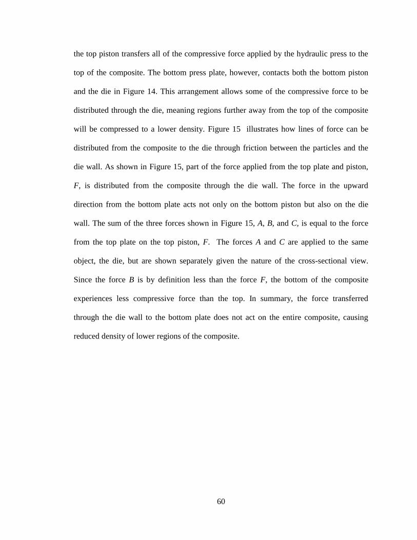
60
the top piston transfers all of the compressive force applied by the hydraulic press to the
top of the composite. The bottom press plate, however, contacts both the bottom piston
and the die in Figure 14. This arrangement allows some of the compressive force to be
distributed through the die, meaning regions further away from the top of the composite
will be compressed to a lower density. Figure 15 illustrates how lines of force can be
distributed from the composite to the die through friction between the particles and the
die wall. As shown in Figure 15, part of the force applied from the top plate and piston,
F, is distributed from the composite through the die wall. The force in the upward
direction from the bottom plate acts not only on the bottom piston but also on the die
wall. The sum of the three forces shown in Figure 15, A, B, and C, is equal to the force
from the top plate on the top piston, F. The forces A and C are applied to the same
object, the die, but are shown separately given the nature of the cross-sectional view.
Since the force B is by definition less than the force F, the bottom of the composite
experiences less compressive force than the top. In summary, the force transferred
through the die wall to the bottom plate does not act on the entire composite, causing
reduced density of lower regions of the composite.
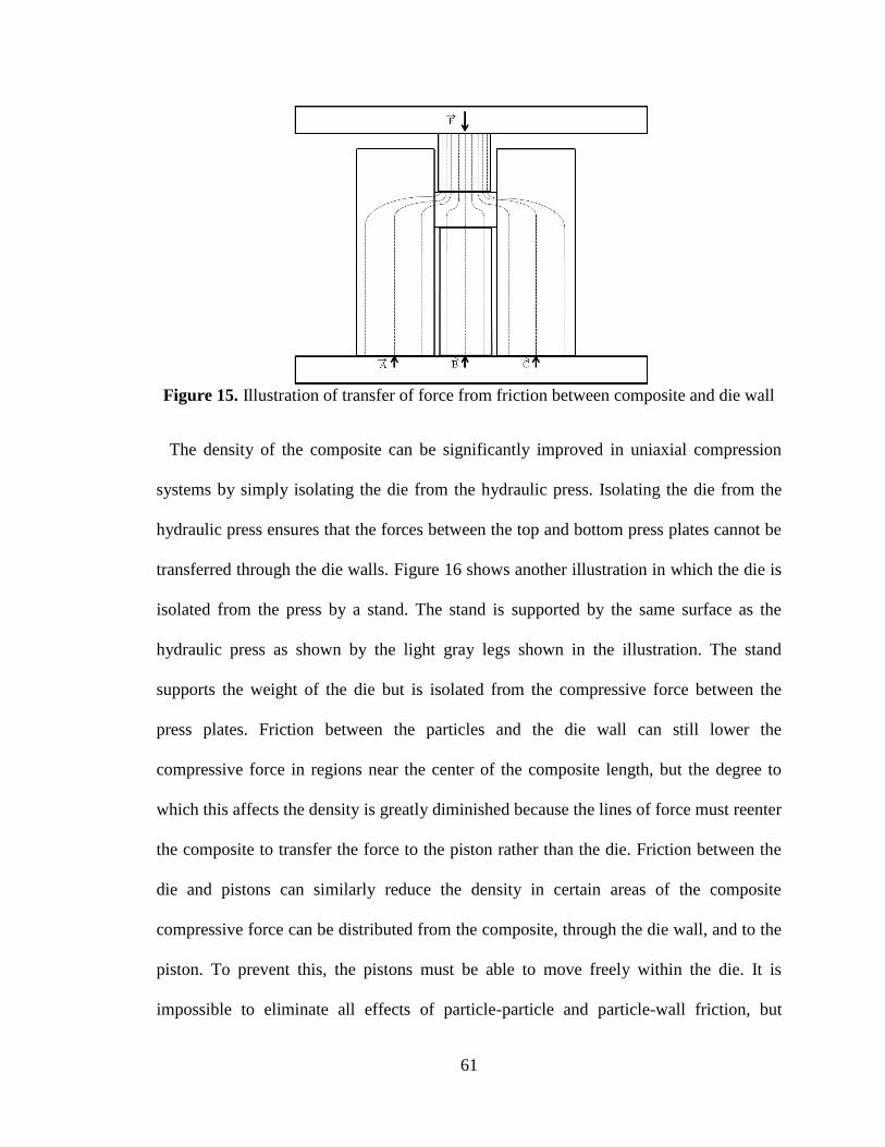
61
Figure 15. Illustration of transfer of force from friction between composite and die wall
The density of the composite can be significantly improved in uniaxial compression
systems by simply isolating the die from the hydraulic press. Isolating the die from the
hydraulic press ensures that the forces between the top and bottom press plates cannot be
transferred through the die walls. Figure 16 shows another illustration in which the die is
isolated from the press by a stand. The stand is supported by the same surface as the
hydraulic press as shown by the light gray legs shown in the illustration. The stand
supports the weight of the die but is isolated from the compressive force between the
press plates. Friction between the particles and the die wall can still lower the
compressive force in regions near the center of the composite length, but the degree to
which this affects the density is greatly diminished because the lines of force must reenter
the composite to transfer the force to the piston rather than the die. Friction between the
die and pistons can similarly reduce the density in certain areas of the composite
compressive force can be distributed from the composite, through the die wall, and to the
piston. To prevent this, the pistons must be able to move freely within the die. It is
impossible to eliminate all effects of particle-particle and particle-wall friction, but

62
additional steps, such as the addition of lubricants during pressing, can also aid in further
compacting the composite. If the lubricant is not a constituent material of the composite,
its benefits in reducing packing friction may be outweighed by its presence in the final
volume of the composite. However, if one of the final constituents of the composite can
be added in a form that is lubricating during pressing, the benefits of lubricated
compaction can be gained without additional materials.
Figure 16. Double-ended uniaxial pressing with an isolated die
2.5 Factors Contributing to High Dielectric Strength
2.5.1 Voids
The presence of voids within a composite can significantly degrade the performance
through the potential for electrical failure of the insulation due to the concentration of the
electric fields in the void. In a simple model of the electric field distribution between the
a void and the surround high dielectric constant material in which a layer comprising the

63
void and a layer comprising the high dielectric material occupy the volume of a capacitor,
a series combination of capacitive layers is effectively formed. The electric displacement
through both layers must be continuous. However, the electric field is not distributed
equally between the layers of different dielectrics. This can be explained through the
constitutive relation describing the electric elasticity without taking into account
nonlinear effects as shown in equation (2.50). The magnitude of the electric field is
represented as E [V/m], and the electric flux density is represented as D [C/m2]. The
permittivity of free space is again ε0 [F/m], and the dielectric constant of the layer is
represented as εr [19].
(2.50)
Analysis of equation (2.44) illustrates how if the electric displacement is equal in both
layers of the capacitor, the electric field in the void will be greater than the electric field
in the high dielectric layer by a factor equal to the ratio of the dielectric constants. This
relation is shown in equation (2.51). The electric fields in the void and the high dielectric
material are represented as Evoid and EHMD, respectively.
(2.51)
It is generally assumed here that the composition of the voids is simply air or other
similar gases. Since the dielectric constant of air is close to unity, the ratio of the
magnitudes of the electric field in the void and in the high dielectric constant material is
approximately equal to the dielectric constant of the high dielectric constant material.
Thus, use of a high dielectric constant material increases the magnitude of the electric
fields in air gaps. This is a risk to the component’s functionality and lifetime. If the

64
electric field in the void is exceeded, there is an increased likelihood of electrical failure
of the high dielectric constant material. Failure of the high dielectric constant material
could occur due to thermal damage, accelerated ions or electrons in the air gap
precipitating breakdown in the high dielectric constant material, or other effects.
Therefore, voids must be minimized not only to limit a decrease in the effectiveness of
the high dielectric constant material as an energy storage medium but also to prevent
accelerated failure of the material as an insulating medium.
Electrostatic simulations of composites generated in CST EM Studio allow the field
distribution between the composite’s components to be visualized and quantified. Full
details on the methods with which the model of the composite was generated and
simulated are presented in Chapter 4. Figure 17 shows a plot of the absolute value of the
3D electric field projected onto the 2D surface of a plane intersecting the composite. The
colored areas are particle cross sections that intersect with the cutting plane, and the
white particles in the background are particles behind the cutting plane. The electric field
on the background particles is not shown.
Figure 17. Plot of 3D fields projected onto a 2D cross section of a composite containing
high and low dielectric constant fillers

65
The virtual composite has a diameter of 10 µm and a thickness of 5 µm. The composite
volume was filled with large particles with a dielectric constant of 1000 and small
particles with a dielectric constant of 1. These values correspond to high dielectric
constant ceramic fillers and air voids, respectively. The remaining composite volume not
occupied by particles was defined to have a dielectric constant of 5. This matrix material
is hidden in Figure 17 to highlight the difference in electric field strength between high
dielectric constant filler particles and low dielectric constant voids. Electrodes on the
upper and lower surfaces of the composite apply a potential of 1 V across the thickness of
the composite. The wide variance in the electric field distribution between particles with
different dielectric constants is evident. Most of the area of the small particles with a
dielectric constant of 1 is filled with dark orange and red indicating electric fields on the
order of 1 MV/m. At the peak electric field value of 1.9 MV/m, the field within the void
particles is 9.5 times the field that would be present in a solid material with a constant
dielectric constant throughout. The field within the void particles is enhanced due to field
concentration by the higher dielectric constant fillers. By contrast, the electric field in the
large particles with a high dielectric constant is generally uniform and very low. There is,
however, evidence of high electric fields towards the upper and lower edges of the high
dielectric constant particles.
Figure 18 shows the same cross-sectional view as Figure 17 with the electric field
plotted in the matrix material with a dielectric constant of 5. The concentration of the
electric field in regions where filler particles are absent is marked by the dark orange and
red regions. The field within this material representing the composite’s binder reaches
values even higher than those observed in the low dielectric constant filler particles at

66
4.28 MV/m. The concentration of fields in certain areas of the binder over others is
partially due to inhomogeneity in the distribution of the filler particles. Improved
homogeneity of the particle distribution will better distribute the electric field within the
matrix material to avoid high peak values that can lead to dielectric failure of the
composite.
Figure 18. 2D plot of the absolute value of the 3D electric field within the matrix
material
2.5.2 Air Gaps at Surface Contacts
Many high power applications of high dielectric constant materials require direct
electrical connections to the high dielectric constant material. Implementation of effective
electrodes to provide this electrical connection is complicated by two significant issues:
1. The surfaces of the high dielectric constant material and electrode must be prepared to
a very high degree of accuracy to eliminate air gaps between the surfaces. 2. Field effect
enhancements at the triple point between the high dielectric constant material, electrode,
and surrounding medium can be very large as a result of the high dielectric constant of
the energy storage material and the geometry of the electrode. Both of these issues are

67
briefly examined, and a proposed solution to make effective electrical connections to
high dielectric constant composite materials is proposed.
For an electrode of a given area, if the interface between the metal of the electrode and
the high dielectric constant material is imperfect, the effective dielectric constant of the
material can be greatly reduced. Figure 19 illustrates how at a microscopic scale, small
imperfections in the surfaces of both the electrodes and high dielectric constant material
can cause significant air gaps to form in the energy storage volume of the capacitor.
Figure 19. Illustration of microscopic imperfections causing air gaps between surfaces.
An effective way to eliminate most air gaps is to directly apply the electrode material in
such a way that will fill all potential areas where an air gap may otherwise form. Several
electrode application options exist, including epoxies loaded with silver or other
conductive elements and deposition through sputtering. Conductive epoxies have the
disadvantage that they contain non-conducting binder materials. At points where the
binder makes direct contact with the high dielectric constant material rather than the
conductive element, a similar effect to that of an air gap is present at that location.
Similarly, if the epoxy is heated to remove the binder elements after application, voids

68
are left that have effects like those described for air gaps. Therefore, although highly-
loaded conductive epoxies can decrease the effects of air gaps, they are not the preferred
option. Sputtering, however, can deposit a thin even layer of metal directly on the surface
of the high dielectric constant material without the use of binders. If the surface of the
high dielectric constant material is prepared with a high grit abrasive prior to sputtering,
an even application of metal by sputtering can form an electrode with minimal air gaps.
Therefore, it is the preferred method for application of electrodes on the high dielectric
material surface. Other steps, including covering the sputtered electrode with a
conductive epoxy, are necessary to prevent abrasion of the thin sputtered contact and
enable external contacts to be made to the electrode.
2.5.3 Triple Points
Triple points are present along the interface between the highly conductive electrode,
the insulating high dielectric constant composite, and the relatively low dielectric
constant surrounding air or other surrounding dielectric material. The triple point is
present along the entire electrode edge as well as at points along the electrode-composite
contact where both ceramic and binder components make contact with the electrode. The
magnitude of the field effect enhancement at the triple point is a function of the dielectric
constants of the materials involved and the geometry of the interfaces, so the application
of the high dielectric constant composites directly contributes to increased field
enhancements. The very small radius of the edges of a sputtered electrode can also
contribute to field enhancement at these triple points.
Reduction of the field enhancement is critical both to avoid premature failure of the
material and to fully utilize the composite’s properties in applications requiring direct

69
electrode connection. The consequences of dielectric failure due to excessively high
electric fields are obvious. However, the effects on reducing the effective energy density
of the material are less apparent. For a capacitive system with a field enhancement factor
of 10, the useful energy density is reduced by a factor of nearly 100 from the peak energy
density, which is only present in a very small volume near the triple points. Minimizing
field enhancements is necessary to utilize the full volume of the material at high energy
densities near its peak capability.
Two approaches have been investigated to address field enhancements due to triple
points at the electrode edge. The first approach mechanically alters the sample and
electrode geometry to remove the triple point from the high electric field region. Grooves
are cut into the composites, forming a reverse mesa structure. The electrodes are then
applied within the groove, preferably by sputtering or another application process that
eliminates air voids at the contact. The result of this geometry is that the triple point
junction of the electrode, high dielectric constant material, and surrounding insulation is
in a much lower electric field region. This approach has been investigated previously in
high power silicon carbide photo-switches [20]. The effectiveness of the embedded
electrodes is demonstrated through simulated electric field plots shown in Figure 20. This
simulation compares the geometry in which the electrode contacts the surface of the
composite and the geometry in which the electrode is effectively embedded 1 mm within
the composite by machining a reverse mesa structure. The electrostatic simulation
performed to produce Figure 20 consisted of a 2.1 mm thick composite with a dielectric
constant of 100 and copper electrodes with 0.5 mm radii on their outside edge. A voltage
of 1 V was applied across the electrodes, and the field levels were compared to those

70
expected from an infinite parallel plate. The 2D plots of Figure 20 have a radial
symmetry around the vertical axis at the left. The triple point in plot (a) corresponds to a
field effect enhancement of 10.43 in the composite material, and the peak fields in the
surrounding air reach 256 kV/m. By embedding the electrode 1 mm into the composite as
in plot (b), the field effect enhancement is reduced to 2.34 in the composite, and the peak
field in the surrounding air is less than 100 kV/m.
Figure 20. Reduction of field enhancement from (a) surface electrodes to (b) embedded
electrodes
A second approach to minimize the field enhancement at the triple points along the
electrode edge is a potentially simpler solution as it does not require precision machining
of the composites. In the second approach, the electrode edges are coated with a high
dielectric constant material that can be applied in a liquid or semi-solid form. By coating
with a high dielectric constant material, the difference in dielectric constants between the
composite and surrounding material at the electrode edge is reduced, decreasing the field
enhancement. This coating approach has also been simulated to evaluate its potential. The
2D plots of Figure 21 have a radial symmetry around the vertical axis at the left. Both
plots are the results of simulations of a composite with a thickness of 0.915 mm and a
dielectric constant of 100. The electrode had a radius in both simulations of 0.1 mm. The
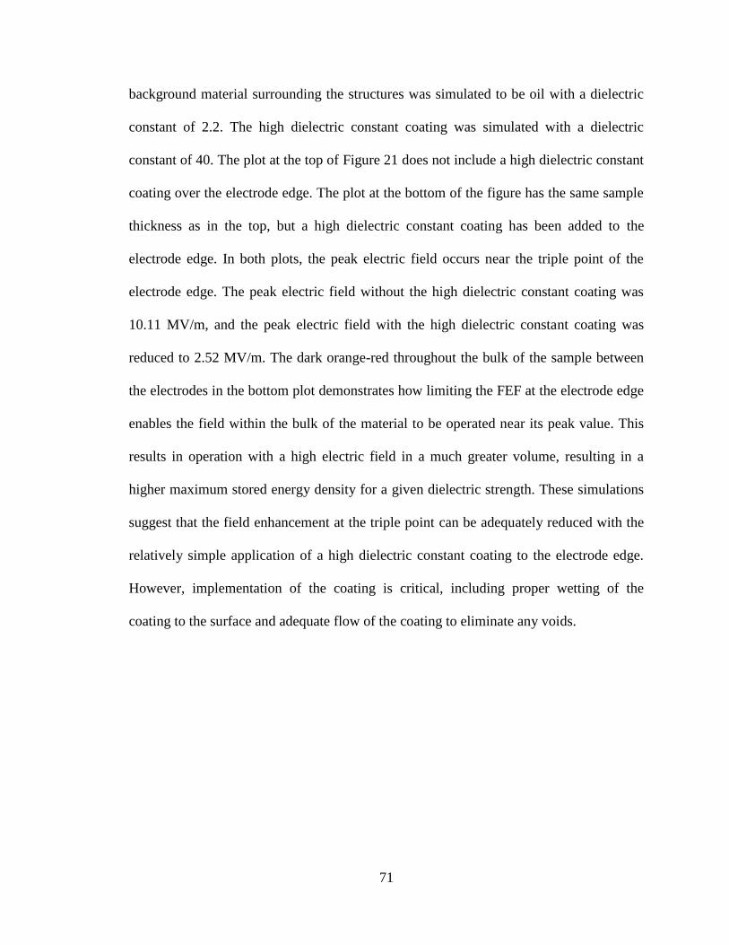
71
background material surrounding the structures was simulated to be oil with a dielectric
constant of 2.2. The high dielectric constant coating was simulated with a dielectric
constant of 40. The plot at the top of Figure 21 does not include a high dielectric constant
coating over the electrode edge. The plot at the bottom of the figure has the same sample
thickness as in the top, but a high dielectric constant coating has been added to the
electrode edge. In both plots, the peak electric field occurs near the triple point of the
electrode edge. The peak electric field without the high dielectric constant coating was
10.11 MV/m, and the peak electric field with the high dielectric constant coating was
reduced to 2.52 MV/m. The dark orange-red throughout the bulk of the sample between
the electrodes in the bottom plot demonstrates how limiting the FEF at the electrode edge
enables the field within the bulk of the material to be operated near its peak value. This
results in operation with a high electric field in a much greater volume, resulting in a
higher maximum stored energy density for a given dielectric strength. These simulations
suggest that the field enhancement at the triple point can be adequately reduced with the
relatively simple application of a high dielectric constant coating to the electrode edge.
However, implementation of the coating is critical, including proper wetting of the
coating to the surface and adequate flow of the coating to eliminate any voids.

72
Figure 21. Simulated electric field in the sample with high dielectric constant coating
(bottom) and without high dielectric constant coating (top)

73
References for Chapter 2
[1] C. Balanis, Advanced Engineering Electromagnetics. Hoboken, NJ: John Wiley &
Sons, Inc., 1989.
[2] Archimerged, "Dielectric responses," Wikimedia Commons, 2008.
[3] R. Simpkin, "A derivation of Lichtenecker's logarithmic mixture formula from
Maxwell's equations," IEEE Transactions on Microwave Theory and Techniques,
vol. 58, pp. 545-550, 2010.
[4] C. F. Yang, C. C. Wu, C. C. Su, and Y. C. Chen, "The development of prediction
method for the permittivity of epoxy/(BaSr)(TiZr)O composites," Applied Physics
A, vol. 97, pp. 455-460, 2009.
[5] T. Yamada, T. Ueda, and T. Kitayama, "Piezoelectricity of a high-content lead
zirconate titanate/polymer composite," Journal of Applied Physics, vol. 53, pp.
4328-4332, 1982.
[6] N. Jayasundere and B. V. Smith, "Dielectric constant for binary piezoelectric 0-3
composite," Journal of Applied Physics, vol. 73, pp. 2462-2466, 1993.
[7] H. Solomon, "Random packing density," in Proc. of the 5th Berkely Symposium
on Mathematical Statistics and Probability. vol. 3, L. Lecam and J. Neyman, Eds.
Berkely, CA, 1965, pp. 119-134.
[8] C. C. Furnas, "Flow of gases through beds of broken solids," US Dept. of
Commerce Bureau of Mines, Washington, D.C. 1929.
[9] C. C. Furnas, "Grading aggregates: I-Mathematical relations for beds of broken
solids of maximum density," Industrial and Engineering Chemistry, vol. 23, pp.
1052-1058, 1931.
[10] F. O. Anderegg, "Grading aggregates: II-The application of mathematical
formulas to mortars," Industrial and Engineering Chemistry, vol. 23, pp. 1058-
1064, 1931.
[11] U. Gesenhues, "Substructure of titanium dioxide agglomerates from dry ball-
milling experiments," Journal of Nanoparticle Research, vol. 1, pp. 223-234,
1999.
[12] V. A. Parsegian, Van Der Waals Forces: A Handbook for Biologists, Chemists,
Engineers, and Physicists. New York: Cambridge University Press, 2006.
[13] "Ceramic Materials for Electronics: Processing, Properties, and Applications," R.
C. Buchanan, Ed. New York: Marcel Dekker, Inc., 1986.
[14] Y. Hwang, J. K. Lee, J. K. Lee, Y. M. Jeong, S. Cheong, Y. C. Ahn, and S. H.
Kim, "Production and dispersion stability of nanoparticles in nanofluids," Powder
Technology, pp. 145-153, 2008.
[15] S. Y. Yao and Z. H. Xie, "Deagglomeration treatment in the synthesis of doped-
ceria nanoparticles via coprecipitation route," Journal of Materials Processing
Technology, pp. 54-59, 2007.
[16] A. Voss and W. H. Finlay, "Deagglomeration of dry powder pharmateutical
aerosols," International Journal of Pharmaceutics, pp. 39-50, 2002.
[17] S. Froeschke, S. Kohler, A. P. Weber, and G. Kasper, "Impact fragmentation of
nanoparticle agglomerates," Journal of Aerosol Science, pp. 275-287, 2003.

74
[18] Sonics, Inc. (December 2008). High Intensity Ultrasonic Processor [Online].
Available:http://www.sonics.com/liquid-datasheet/VCX500-
VCX750%20new%20micro.pdf.
[19] F. T. Ulaby, Fundamentals of Applied Electromagnetics. Upper Saddle River, NJ:
Prentice Hall, 2001.
[20] C. M. Fessler, K. Kelkar, W. C. Nunnally, and N. E. Islam, "Investigation of high
electric fields at the electrode-SiC interface in photo-switches," in 2007 16th
IEEE Inter. Pulsed Power Conf. Albuquerque, NM, 2007, pp. 114-119.

75
Chapter 3: Development of High Dielectric Constant
Composite Materials
3.1 Literature Survey of High Dielectric Constant Composites
A brief review of notable works in the field of high dielectric constant composites is
provided before discussing the critical factors involved in creating high dielectric
constant composites and the approaches taken in this program. The majority of research
on high dielectric constant composites has focused on thin film applications for very
small scale components. Most of these composites have been designed for low power
applications, and many of the requirements and constraints differ from the present effort.
Nevertheless, the basic effort of developing high dielectric constant polymer-ceramic
composite materials is a common goal between these works and the present effort, so an
overview is appropriate. The review provided here cannot be considered exhaustive due
to the many works on composite materials, but many of the most notable high dielectric
constant results are given for comparison to the results achieved in this program. Since
the inception of this work, a review of research on composites has been produced for
pulse power energy storage applications [1]. While several of the works referenced in that
review are noteworthy, energy storage applications often have a priority towards high
electric field operation. While high field operation is important in this work as well, a
high dielectric constant is necessary to achieve reduction of the antenna size.
Table 2 provides an overview of the works included in this review. The first authors
listed in Table 2, excluding Borchardt, are from Georgia Tech University. Their work has
concentrated on very thin films for embedded capacitor applications, but it has resulted in
many of the highest known dielectric constant composites previously produced.

76
Table 2. Notable Previous Works in High Dielectric Constant Composite Materials
Researchers Ceramic
Material
Matrix
Material
Thickness
(mm)
Percentage
of Ceramic
(vol%)
Frequency of
Measurement
(MHz)
Dielectric
Constant
Rao et al [2]
Bimodal
PMN-PT
and BTO
High K
Epoxy 0.00375 85 1800 140
Windlass et
al [3]
Bimodal
PMN-PT
and BTO
Epoxy 0.003 85 Unspecified 135
Rao et al [4]
Bimodal
PMN-PT
and BTO
High K
Epoxy 0.01 70 100 100
Agarwal et
al [5]
Bimodal
BTO Epoxy ~ 0.003 Unspecified Up to 0.1 74
Ogitani et al
[6] PMN-PT
Photo-
definable
Epoxy
0.01 71 0.1 70
Borchardt
et al [7] BST Epoxy
Up to
1.27 Unspecified Unspecified 50
The first material listed in Table 2 was prepared as a polymer-ceramic composite
containing both lead magnesium niobate-lead titanate (PMN-PT) and barium titanate [2].
PMN-PT is noted to have a dielectric constant several times that of barium titanate with
the values referenced by Rao et al as 19,316 and 3,000, respectively [2]. PMN-PT is
often, therefore, a very attractive material for high dielectric constant composites. It
should be noted that PMN-PT and other lead-based ceramics were excluded from
consideration for the composites developed in this work due to the potential health
hazards of lead-based materials. The PMN-PT and barium titanate used by Rao were
mixed in a bimodal distribution with particle sizes of 0.9 and 0.05 µm, respectively,
resulting in a particle size ratio of 18:1 [2]. The volume ratio of PMN-PT to barium
titanate was 4:1. The binder was an epoxy with an enhanced dielectric constant. The
binder, Dow Epoxy Resin 661, was modified by 5 wt% cobalt (III) acac, which was used
as a curing catalyst to increase the binder’s dielectric constant to 6.4 [2]. The ceramic

77
mixture was loaded into the binder at 85% by volume, and the composite was formed to a
thickness of 3.75 µm [2]. The dielectric constant was measured over the frequency range
of 10 kHz to 1.8 GHz. The low frequency dielectric constant was measured to be 150,
and the dielectric constant remained high at approximately 140 above 1 GHz [2]. The
dielectric strength of the composites was measured with a DC supply to reach 17 MV/m
[2]. A very similar work by Rao et al is listed as the third entry in Table 2. That work was
published in the same year as the first table entry, and many of the experimental
parameters are the same. The dielectric constant values reported in the second work are
slightly lower than the first with a value of 100 at 100 MHz [4]. The difference is likely
due to the lower ceramic loading percentage, which was 70% by volume in the measured
sample [4]. Other variations in the second work included a barium titanate particle size
increase to 0.65 µm and a PMN-PT to barium titanate volume ratio of 3:1. The dielectric
constants measured in Rao’s work are the highest found for a polymer-ceramic composite
and exhibit exceptional stability over a wide frequency range.
The second entry in Table 2 authored by Windlass et al primarily discusses issues of
ceramic particle treatment, dispersants, and solvents in spin-coated thin film composites
for embedded capacitor applications [3]. The article examines the production of a
bimodal mixture of PMN-PT and barium titanate. However, the notable dielectric
constant reported, 135, is referenced only as a PMN-PT and epoxy composite [3]. The
optimal volume percentage of ceramic is noted to be 85% as it is claimed that higher
percentages result in porosity due to insufficient filling of the remaining volume with
polymers. The author mentions work on films with thicknesses between 2 and 4 microns,
78
and the dielectric constant value of 135 is believed to be from a 3 µm film. No
information is included on the measurement frequency.
Agarwal et al reported a work that exhibits the highest previous dielectric constant
without lead-based ceramics [5]. The highest dielectric constant measured by Agarwal et
al was 74 for a bimodal distribution of barium titanate in epoxy [5]. The bimodal
distribution was composed of large particles of 200 nm and small particles of 20-30 nm
[5]. The frequency of the dielectric constant measurement of 74 was not specifically
reported, but it is noted that the measurements were taken with an LCZ meter capable of
measurements up to 100 kHz [5]. The volume percentage of ceramic was not reported for
the film with a dielectric constant of 74, but the ratio of large to small particles was
reported as 5:1. The thin film with a dielectric constant of 74 was formed by dip coating
from a colloidal solution of the ceramic and epoxy in methyl ethyl ketone (MEK). The
thickness of the film was not specifically reported, but it was noted that thin films were
produced. Other films included in the study were reported with a thickness of
approximately 3 µm, and that thickness is considered representative for the films in that
study [5].
The final thin film high dielectric constant composite described here was reported by
Ogitani et al. The peak dielectric constant measured in that study was approximately 70
up to 100 kHz [6]. The composites were made from epoxy loaded to 71% by volume with
PMN-PT [6]. The ceramics were treated with a phosphoric acid surfactant to improve
particle dispersion through an acid-base reaction with the PMN-PT surface [6]. The
particle size distributions were centered around 1 µm, but the actual sizes were dependent
on the ball mill and surfactant treatment. A final film size of approximately 10 µm was

79
obtained through spin coating. It was noted that the composite with a dielectric constant
of 71% had some negative physical properties due to light scattering by the particles
degrading the photo-definable epoxy. Therefore, the particle loading was generally
limited to 65%, which resulted in a dielectric constant value of 62 [6].
The notable works reviewed here represent substantial improvements in high dielectric
constant composites. However, the applicability of these composite materials to high
power systems is very limited. The composites reviewed thus far were developed for
embedded capacitors or other thin-film chip-based requirements. The very small
thicknesses would not withstand substantial voltages despite the respectable dielectric
strength observed by Rao et al. Even at a dielectric strength of 17 MV/m, a 3 µm film
would fail at 51 V. Therefore, high dielectric constant composites developed specifically
for high power applications are required. The amount of previous research into high
power composites is much smaller that devoted to embedded capacitor research. Only
one notable previous study on high dielectric constant composites for high power
applications is known. Borchardt et al reported on a high dielectric constant composite
built for high energy density capacitors developed in a collaborative effort between
Sandia National Laboratories and TPL, Inc. [7]. The article focuses on capacitor
development, and relatively little specific information is given on the material. However,
it was noted that nanoparticulate ceramics were mixed with a two-part epoxy system to
form the composites [7]. The dielectric constant of the material developed by TPL Inc. is
reported to be 50, but the frequency of the measurement was not reported [7]. The
thicknesses of the composites were reported to typically be between 0.5 mm and 1 mm
with a maximum reported thickness of 1.27 mm. While this is not a substantial thickness

80
for some applications, it is orders of magnitude larger than thin film technology. The
highest average dielectric strength reported for single-layer capacitors formed with the
material corresponds to 149.6 MV/m. The material energy density at this field reaches
nearly 5 J/cm3, but it was noted that capacitors formed with the material had only been
shown to operate consistently at 0.6 J/cm3 [7]. Dielectric strength measurements using
spherical electrodes with diameters of 16 mm obtained average values corresponding to
334.6 MV/m. Although the dielectric constant of the material developed by TPL Inc.
does not reach as high of dielectric constant values as the previously-reviewed thin-film
composites, a dielectric constant value of 50 represents a significant milestone for
relatively thick substrates of high dielectric constant materials. Along with the high
dielectric strength, the material developed by TPL Inc. was the benchmark for
comparison of the high dielectric constant composites developed as a part of the effort
described in this proposal.
3.2 Novel Approaches to High Dielectric Constant Composite
Development
The high dielectric constant composite materials developed in this effort have multiple
unique features from previously-developed composites in their composition, fabrication,
and properties. The following three points have been singled out for discussion as novel
approaches that result in extraordinary dielectric properties.
1. Trimodal Particle Packing: A trimodal distribution of particle sizes in which
ceramic particles ranging from less than 100 nm to greater than 100 µm is
implemented to increase the ceramic packing factor.

81
2. In-situ Polymerization of Coupling Agents: Polymerization of the polymer is done
in-situ, in which polymer precursors are mixed and compressed with the ceramic
particles prior to the onset of polymerization and cross-linking. This method further
increases the packing factor and boundary interfaces over composites formed with
pre-polymerized macromolecules. While other works have also employed in-situ
polymerization, the use of coupling agents as the sole binder in the composite
minimizes the volume occupied by the binder and promotes strong binding to the
particle surfaces.
3. Void-Filling with High Dielectric Constant Fluids: Dielectric fluid, including high
dielectric constant fluids, can be used to replace any remaining composite voids to
eliminate space occupied by air, improving the composite dielectric constant and
dielectric strength.
3.2.1 Trimodal Particle Packing
As discussed earlier in this chapter, the effective dielectric constant is determined by
the volume percentage of the each of the composite’s constitutive components.
Therefore, for the highest effective dielectric constant, the volume percentage of the
components with the highest dielectric constant should be maximized, and the volume
percentage can be maximized by efficient packing of the component with the highest
dielectric constant by utilizing multiple particle sizes. Bimodal particle distributions have
been effectively employed in previous high dielectric constant composites to produce
some of the notable works reviewed in Chapter 2 [2-5]. However, the ratio of particle
sizes and the relative amount of each particle size were not optimized in those studies for
the maximum packing density. The ultra-thin nature of those composites were likely

82
limiting factors in the ratio of particle sizes, and few details are provided on how the
relative amounts of each particle size were obtained. The large thickness requirement of
high power composites enables a much larger ratio of particle sizes to be employed, so
trimodal distributions are possible in which relatively large particles of many tens or even
hundreds of microns can be used. The dielectric strength of the composite is considered
to be the limiting factor on the size of the particles. Since defects in the structure of a
particle could cause dielectric breakdown of the entire composite if the particle composed
a large fraction of the composite’s thickness, the maximum dimension of any particle is
limited to approximately one-tenth the minimum thickness of the composite.
Due to the processes with which perovskite ceramic powders are manufactured and the
common tendency to strictly use nanoparticles or particles with dimensions of only a few
microns, powders with dimensions on the order of tens of microns or larger are generally
unavailable. Therefore, a method for producing particles in this size range had to be
developed. Sintered pieces of the ceramic between 3 and 12 mm, which are traditionally
sold for vacuum deposition applications, are purchased commercially. The pieces are
then sintered again in air for 3 hours at 1350 C to further improve their density. After
sintering, the pieces are milled and sieved to the desired size range.
By combining three particle sizes, the composites have a unique distribution of particle
sizes ranging from nanoparticles with dimensions of approximately 50 nm to
microparticles with dimensions of 50 µm and greater. To maintain approximately the
same ratio between the intermediate-sized particles and small particles and the large
particles and intermediate particles, the intermediate sized particles should be
approximately 1.6 µm. Such a large range of particle sizes represents a novel

83
advancement in high dielectric constant composites and enables a higher degree of
particle packing and correspondingly larger dielectric constant.
3.2.2 In-situ Polymerization
A binder is necessary to provide the mechanical integrity of a composite made with
ceramic particles without sintering. Previous studies of high dielectric constant
composites have implemented a wide variety of polymers and epoxy compounds to bind
the composite. The approach of mixing polymers with ceramic particles prior to
composite formulation generally assumes that the polymers will fill the voids between
ceramic particles [3]. This approach appears to be theoretically sound for relatively low
loading levels of ceramic particles in which the polymer has ample space to fill between
particles. However, when the ceramic particle density is maximized according to the
methods previously described, the voids between particles can be much smaller than the
dimensions of most polymers. In such a situation, the addition of polymers larger than the
voids result in an increase in the size of the composite and a decrease in the ceramic
particle density. Therefore, in composites intended to have a very high density of ceramic
particles, the design must limit not only the amount of polymer that is added to the
system but also the size of the polymer chains.
By definition, polymers are large macromolecules with repeating units. As an example,
the typical dimensions of a common polymer implemented in polymer-ceramic
composites, polyvinylidene fluoride (PVDF), are considered. PVDF consists of a
repeating structure of (CF2 – CH2)n units [8]. The carbon-carbon bond length is
approximately 157 pm at an angle of 100 degrees. This corresponds to a unit length of
approximately 120 pm. The average molecular weight of commercially-available PVDF

84
can vary widely, and a recent survey of offerings from Sigma-Aldrich had a low-end
value of 180,000. This molecular weight corresponds to approximately 2,800 repeating
units and a polymer contour length of slightly greater than 350 nm. The width of the
polymer chain is substantially smaller, with a contour width having been measured for
poly(2-vinylpyridine) with an atomic force microscope to be approximately 0.4 nm [9].
The polymer chains form coils with different degrees of compactness ranging from being
extended chains to compact globules. However, even compact globules formed by
poly(2-vinylpyridine) were measured to have a radius of gyration between 20 and 30 nm
[9]. The radius of gyration for extended chains was closer to 60 nm [9]. The large contour
length and radius of gyration can make them incompatible for filling very small voids. If
the polymers being added to a bed of ceramics are on the same size scale as the smallest
ceramic particles, the polymers will displace some of the volume that should be occupied
by ceramic particles and lower the effective dielectric constant. For polymers to
effectively fill the voids between ceramic particles in a packing of maximum density, the
polymer dimensions must be much smaller than the dimensions of the smallest ceramic
particle. If the smallest ceramic particle size is approximately 50 nm, then the polymer
dimensions must be less than 10 nm. Such small dimensions are uncommon for
traditional polymers, so a novel approach must be made to form the binder network.
The novel approach developed to minimize binder molecule size and retain a high
ceramic particle packing factor has two components, including in-situ polymerization and
the selection of unique binder networks. In-situ polymerization is briefly described here,
and the unique binders are detailed in the following materials section. In-situ
polymerization describes how the formation of polymer chains is delayed until after the

85
composite has been formed. With this approach, the precursor chemicals needed for
polymer formation are mixed into a slurry with the ceramic particles. The slurry is then
compacted in a press, so the polymer precursors only remain in the small voids between
ceramic particles. After this compaction, polymerization is initiated such that the polymer
can only form in the confined spaces of the inter-particle voids. Thus, the decrease in the
ceramic particle density resulting from the addition of pre-polymerized macromolecules
to the ceramic mixture is avoided.
3.2.3 Void-Filling with High Dielectric Constant Fluids
At the nanometer and sub-nanometer scale, even well-designed, highly-packed
composites will have some voids present that cannot be filled with additional ceramic
particles or polymers. It is, therefore, beneficial to examine alternative methods for filling
the remaining voids. To penetrate to the location of the voids with a small enough
chemical structure to fill the sub-nanometer dimensions along particle surfaces, a non-
viscous fluid is normally required. The fluid could be either a gas or a liquid. In some
limited circumstances in which the composite is used in an air-tight enclosure, filling the
voids with sulfur hexafluoride (SF6) or a high pressure gas could significantly increase
the dielectric strength of the composite. However, it is normally much more practical to
fill the voids with a liquid, which can remain in the voids for a much longer timeframe
than a gas.
Liquid filling of composite voids offers the additional advantages of a wide variety of
liquid properties that can be advantageous to add to the composite. Similar to the
potential use of SF6, dielectric liquids, including oils commonly used for high voltage
electrical insulation, can fill the voids to increase the dielectric strength beyond that

86
obtained with air-filled voids. The higher dielectric constant of the oil can also increase
the effective dielectric constant of the composite. While the increase of the effective
dielectric constant may only be marginal when using insulating oils, fluids with excellent
dielectric strength and very high dielectric constants are available that can substantially
increase the effective dielectric constant when used as void fillers. In addition to a high
dielectric strength and high dielectric constant, the ideal void-filling fluid has low
dielectric losses and a low evaporation rate. A low vapor pressure is necessary for the
liquid to be retained in the composite for a suitably long time before the dielectric
properties begin to change. The materials identified as good void-filling fluids are
described further in the following materials section.
3.3 Concepts of the Classes of High Dielectric Constant Composites
Each of the three composite classes developed in this work is based on a different
concept for how the binder enables the effective dielectric constant of the composite to be
enhanced. To provide context to the discussion of materials selection, this section first
provides a brief description of the concepts behind each of the composite classes.
3.3.1 Composite Class 1 – MU45
MU45 was the first of the three composite classes to be developed, and as such, it
employs the most conventional approach of the three high dielectric constant composite
classes. The approach to MU45 is conventional in that the dielectric constant is increased
by combining perovskite ceramic materials with a highly polar binder. By using a polar
binder with a high dielectric constant, both of the major composite components have a
high dielectric constant. This approach has been explored many times by other

87
researchers, and polyvinylidene fluoride is a commonly used polar polymer for this
approach. The binder chosen for MU45, cyanoethylated pullulan, has more recently been
studied for this approach due to its dielectric constant being approximately 1.75 times
higher [10]. Cyanoethylated pullulan has been incorporated into at least two previous
polymer-ceramic works on high dielectric constant composites [10, 11].
MU45 is unique compared to previous works incorporating cyanethylated pullulan in
two ways. First, MU45 utilizes ceramic particles in three distinct particle size ranges
according to the previously discussed trimodal particle packing. The use of trimodal
particles significantly increases the particle packing density over that achievable with
particles of a single size distribution. The volumetric density of ceramic particles is thus
the highest of all materials forming the composite. The polymer content is minimized
while ensuring that the mechanical integrity of the composite is maintained. Second,
MU45 was produced as a bulk material in contrast to the thin films developed by other
researchers. Previous works on composites including cyanoethylated pullulan focused on
this films between 100 and 500 µm [10, 11]. MU45 was routinely produced at
thicknesses on the order of millimeters up to a few centimeters.
3.3.2 Composite Class 2 – MU100
The MU100 composite class is unique by the choice of the binder material and the in-
situ polymerization of the binder after the ceramic particles have been fully compacted.
By delaying polymerization of the binder until after the composite materials have been
fully compressed, the volumetric polymer content is minimized. This application of in-
situ polymerization restricts the polymer content to only filling the natural voids between

88
ceramic particles ideally without increasing inter-particle distances. In other composites
that simply mix ceramic particles with pre-polymerized macromolecules, the packing of
the ceramic particles is limited by the space in which the long polymer chains already
occupy. With in-situ polymerization, the polymer chain length and volume is limited by
the space available between packed ceramic particles.
The binder employed in MU100 is also unique. While many polymer-ceramic
composites functionalize the surfaces of the ceramics with a coupling agent to improve
particle dispersion and interface to another binder, MU100 eliminates the extra binder
and achieves mechanical integrity through the sole use of coupling agents. The binder
takes the form of a polysilsesquioxane that directly bonds to the surfaces of the ceramic
particles and cross-links into a three-dimensional network.
MU100 also utilizes a trimodal distribution of ceramic particles. As in the first
composite class, the three size ranges of ceramic particles allow for a greater volumetric
density of the high permittivity material. The volumetric polymer content is minimized
through in-situ polymerization and the selection of a polysilsesquioxane binder. Thus,
MU100 uses the first two of the three concepts listed in section 2 of this chapter.
3.3.3 Composite Class 3 – MU550
The concepts behind the MU550 composite class make it likely the most novel of the
three composite classes. MU550 utilizes the first and third concepts presented in section 2
of this chapter. Of particular importance is that MU550 uses liquid fillers to displace the
voids within the composite. By incorporating both solid and liquid phases into its
structure, MU550 has a hybrid nature. To facilitate the impregnation of the liquid filler

89
throughout the composite, a composite formation process has been developed to form a
network of small channels along the binder network through which the liquid filler can
flow.
The binder for the hybrid composite is a water-gelling thermoreversible polymer. The
polymer is added to the ceramic particles while melted in water. The ceramic particles
and binder are compacted while the binder is in this melted wet state. As the polymer
cools, it forms a gel with the water content that has not been removed during compaction
of the mixture. The particle density is able to remain high with this polymer due to the
wet pressing technique and the manner in which the gel forms as the mixture is cooled.
The composite is then heated to a temperature below the polymer melting temperature to
remove the water from the gel. The gel structure does not collapse as the water is
removed due to the supporting structure of the ceramic particles, but the removal of the
water leaves a substantial number of void channels throughout the binder network that
can then be filled with a fluid that does not cause the binder to gel. In this way, the
volume of the polymer is minimized by removing the water, and the mechanical integrity
of the composite is maintained by replacing the water with a fluid that does not form a
gel.
As with the other composite classes, a trimodal size distribution of ceramic particles is
used to maximize the particle packing density. The trimodal particle distribution of the
MU550 composite is the same as the distribution used in MU45 and MU100. Since the
binder is not fully formed while the composite is compressed and excess binder can be
squeezed out, the density of the trimodal particle distribution in MU550 can reach
approximately the same levels as that obtained in MU100.

90
3.4 High Dielectric Constant Ceramics
The ceramics incorporated into the composites are the highest dielectric constant
material, so the volume percentage of ceramic content is maximized. Some ceramics
exhibit extremely large dielectric constant values due to their perovskite structure. This
section provides a theoretical background on perovskite ceramics followed by details
behind the selection of the ceramic used in the high dielectric constant composites.
3.4.1 Overview of Perovskite Ceramics
Perovskite materials have been of significant interest for more than sixty years.
Applications of perovskite materials were first independently studied by several countries
during World War II, primarily due to their ferroelectric and piezoelectric properties [12].
Since then, many types of perovskite materials have been created in the laboratory with a
wide range of properties and potential applications [12].
Despite the variety of perovskite materials and unique properties that have been
developed, perovskite materials with ferroelectric and piezoelectric properties remain of
primary interest in electrical engineering for their applications in energy storage, energy
transducers, high dielectric constant materials, and sensors. Many researchers have
investigated composite materials with perovskites to incorporate their ferroelectric and
piezoelectric properties with materials having improved mechanical properties. As the
composites have improved, perovskite nanoparticles have been implemented. This
section will detail perovskite materials, focusing on their structure, ferroelectric and
piezoelectric properties, and two methods of nanoparticle synthesis.
91
Perovskite materials receive their name from their common structure to calcium
titanate (CaTiO3), which is traditionally referred to as perovskite [13]. Perovskites have
the basic chemical formula given in equation (3.1).
(3.1)
The symbols A and B represent positively charged metal cations. The formula of equation
(3.1) can become more complex for more exotic perovskites. A solid solution can be
formed by two metal cations in ratios that total one for the A component, as given in
equation (3.2). The symbol x is a number between zero and one.
(3.2)
More exotic perovskites have been developed with two or more elements represented by
B in equation (3.2) [12]. Above the Curie temperature, most perovskites have the cubic
structure. In the case of CaTiO3, calcium ions are located at the eight corners of the
structure. The titanium ion is centered in the cube. Lastly, the oxygen atoms are found at
the center of the faces.
One of the perovskites of particular interest due to its ferroelectric and piezoelectric
properties is barium titanate, BaTiO3. As the similarities of its chemical formula to
calcium titanate implies, the calcium ions of calcium titanate are replaced by barium. The
coordination of the cations can be determined for barium titanate based upon the unit cell.
The titanium ion at the center of the cell is coordinated with the six oxygen ions at the
face centers. The barium cations at the corners are coordinated with twelve oxygen
atoms.
The cubic structure is useful in describing the arrangement and coordination of
barium, titanium, and oxygen atoms, but barium titanate is most often used in

92
applications with other unit cell structures. Below the Curie temperature, barium titanate
takes on a tetragonal structure [12]. The tetragonal structure distorts the symmetry of the
cubic structure. One of the side lengths is longer than the other two sides. This distortion
results in a loss of charge symmetry and a net electrical dipole. This phenomenon is the
basis for the ferroelectric property of perovskite materials.
Perovskites are notable as high dielectric constant materials due to their ferroelectric
properties [14]. The spontaneous polarization of ferroelectric materials is responsible for
electrostatic energy storage in the electric dipole formed in the material’s lattice. The
polarization of the material is dependent on the history of the electric field applied to the
material. Figure 22 provides an example of a hysteresis loop for a perovskite material.
Figure 22. Example Hysteresis Curve of a Perovskite Material
After the electric field, E, applied to the material is removed, the polarization or electric
flux density, D, does not go to zero. Instead, ferroelectric materials exhibit a remnant
polarization. The polarity and magnitude of the polarization is dependent on the history

93
of the applied electric field. The similarities of the hysteresis curve to the B-H curves of
ferromagnetic materials influenced the naming of ferroelectric materials [15].
As discussed in Chapter 2, the polarization and the electric field are related by the
permittivity. Therefore, the dielectric constant can be taken as the slope of the path
followed in Figure 3 when normalized by the permittivity of free space. When the
magnitude of the electric field is less than its saturation value, Esat, the slope of the curve
and the dielectric constant are very large. This is the normal region of operation of the
material in energy storage devices. When the magnitude of the electric field is greater
than the saturation value, the material is considered saturated and the dielectric constant
is significantly lower. Saturation of the material can be understood as the alignment of all
the domains of electrical dipoles in the material. Saturation of the material is avoided is
standard applications of ferroelectric materials, such as in capacitors. In addition to the
dependence of the dielectric constant to the applied electric field, the dielectric constant
has a high dependence on the temperature and frequency of operation.
Another interesting property of some perovskite materials is the piezoelectric effect.
The piezoelectric effect relates the strain on the material to the applied or induced voltage
[16]. The direct piezoelectric effect describes the voltage induced across the material due
to an applied stress, T [Pa]. When no stress is applied, there is no electric displacement
induced. However, when a stress is applied to the material, an electric displacement is
induced. The presence of a voltage across the material when a stress is applied can be
attributed to the distortion of the lattice, causing electric dipoles. In this case of the
converse piezoelectric effect, an electric field, E [V/m], is applied to the material.
Without the electric field, the induced stress, S [Pa], in the material is zero. However,

94
when the electric field is applied, a stress is induced in the material. Again the
relationship between the electric field and the stress can be attributed to the distortion of
the lattice, creating a small change in the material dimensions.
3.4.2 Selection of Ceramic Material
As evidenced by its use in several of the notable works cited at the beginning of this
chapter, PMN-PT is an attractive option as the ceramic material. It exhibits a dielectric
constant more than six times higher than that of barium titanate [2]. However, PMN-PT
and many other lead-based and other perovskites were not considered eligible materials
in the development of the composites due to their health risks and the lack of handling
equipment to manage those health risks. Since the composites must be machinable, the
creation of toxic dusts or flakes when cutting composites with lead or other toxic
compounds is unacceptable. If the requirements of a high dielectric constant composite
are changed such that the machining capability or the resulting health risk is minimized,
replacing the ceramics used in this work with PMN-PT or other perovskites could offer
dielectric properties much higher than those achieved in this work.
Another common substitute for barium titanate is the solid solution of barium strontium
titanate. The relative amounts of barium and strontium are adjusted to change the Curie
temperature between that of pure barium titanate and that of pure strontium titanate. The
Curie temperatures for barium titanate and strontium titanate are approximately 120 C
and -168 C, respectively. By tuning the Curie temperature to be around the operating
temperature of the ceramic, the dielectric constant of the ceramic can be greatly
enhanced. An example of tuning the Curie temperature is provided in Figure 23 [17]. The
graph shows the dielectric constant and losses with respect to frequency and temperature

95
for Ba0.6Sr0.4TiO3 produced by TRS Technologies Inc. The added strontium in
comparison to barium titanate has the effect of lowering the Curie temperature from
around 120 C for barium titanate to around 5-10 C in Figure 23. The peak in the dielectric
constant at the Curie temperature is very pronounced as the dielectric constant is more
than five times the typical value below the Curie temperature.
Figure 23. Dielectric constant and dielectric loss of 60/40 barium strontium titnate as a
function of temperature and frequency. Data included with permission of TRS
Technologies [17]
Despite the significant increase in the dielectric constant, there are two negative aspects
of operating near the Curie temperature. As seen in Figure 23, the peak in the dielectric
constant is relatively narrow, resulting in a high dependence of the dielectric constant on
temperature. Above the Curie temperature, the lattice structure is cubic, and the dielectric
constant decreases with increasing temperature. Below the Curie temperature, the lattice
structure is tetragonal for a wide temperature range. Although the dielectric constant
decreases rapidly from its peak at the Curie temperature, the dielectric constant in the
temperature range at which the lattice structure is tetragonal is relatively flat. A second

96
negative aspect of operating near the Curie temperature is increased dielectric losses.
While the losses are highly frequency dependent, a peak in the dielectric losses, denoted
by the empty circles in Figure 23, is evident near the Curie temperature.
Since the composites developed in this effort have a requirement for operation over a
wide temperature range, barium titanate is used rather than barium strontium titanate to
reduce the variation in the composites’ properties with temperature. Although this
selection reduces the peak effective dielectric constant achievable by the composites, it
provides much greater temperature stability and a wider variety of potential applications.
3.5 Binder Materials
Since the three composite classes developed in this work differ significantly in the
concepts behind how the dielectric constant is increased, the specific properties desired
for the binder in each composite are dependent on the method of composite formation. In
general, a low molecular weight was considered advantageous for efficient particle
packing as described in Chapter 2. The binders and their properties are significantly
different, so each is described independently in the context of its intended application.
3.5.1 Cyanoethylated Pullulan
Cyanoethylated pullulan is the binder used in the MU45 composite. The base of this
polymer, pullulan, is a common polysaccharide [18]. The high polarity of the binder
arises from the cyanoethylation of the pullulan [11]. Cyanoethylation refers to the
chemical addition of acrylonitrile to a compound with a hydroxyl group [19].
Acrylonitrile and nitriles in general contain the cyano functional group, consisting of a
carbon-nitrogen triple bond. This carbon-nitrogen triple bond is highly polar due to the

97
strong electronegativity of the nitrogen atom. The addition of the acrylonitrile groups
along the pullulan imparts a net polarity to the binder as a whole.
The cyanoethylated pullulan was obtained commercially through Shin-Etsu Chemical
Co., Ltd. Shin-Etsu markets four products as cyanoresins, and the cyanoethylated
pullulan is used in this work is referred to as CR-S. A softening point is reported at 90-
110 C. CR-S is reported to have a dielectric constant of 18 at 20 C and 1 kHz. The
dielectric constant of CR-S has been reported to be 21 at 1 kHz [10]. However, as with all
other known highly polar polymers, the dielectric constant decreases significantly with
frequency before the VHF and UHF bands. It was noted in the previous study that the
peak of the dielectric losses was observed at approximately 4 MHz [10]. This indicates
that 4 MHz is a resonant frequency for the polarization mechanism of CR-S, and the
dielectric constant decreases significantly above approximately 10 kHz [10]. While CR-S
is one of the best polar polymers available to form high dielectric constant composites in
a conventional method, the effectiveness of these polar polymers is limited at the high
frequencies on interest for antenna applications.
3.5.2 Polysilsesquioxanes
Coupling agents, including silanes and titanates, are commonly applied to particle
surfaces in composite systems [20, 21]. The coupling agents are conventionally employed
as buffers between the inorganic chemistry of ceramic fillers and the organic chemistry of
polymers [20]. Many properties are cited as being improved by uniting the two phases of
the composite with a coupling agent, including the particle dispersion, electrical and
mechanical properties, rheological control, and particle surface wetting [20]. Titanates
are claimed to have additional potential due to the increased number of functional groups

98
on a titanate compound [21]. However, details are provided here on silane coupling
agents only due their more extensive use and more developed technology.
Silanes of particular interest can be classified as organofunctional alkoxysilanes and
have the general formula of equation (3.4) [22]. The symbol R’ represents an alkoxy
moiety, and although the symbol n can be a number between 1 and 4, the class of interest
has an n value of 1, representing trialkoxysilanes [22]. The symbol R represents a non-
hydrolyzable organic group [22].
(3.4)
The alkoxy moieties are often methoxy or ethoxy, and these groups easily hydrolyze and
later bond to inorganic surfaces containing hydroxyl groups [22]. The organic group
represented by R provides compatibility with organic binders and is considered an
organofunctional group. Table 3 shows three examples of trialkoxysilanes that can be
used as coupling agents.
Table 3. Examples of Trialkoxysilanes for Particle Functionalization or Formation of
Polysilsequioxane
Silanes have been effectively implemented as coupling agents in previous composites
incorporating barium titanate and barium strontium titanate [23, 24]. It has been shown
that a pre-treatment of the particles in hydrogen peroxide can increase the number of
hydroxyl groups with which the silanes can bond, creating more sites for coupling
between the inorganic and organic phases [25]. Using these methods, silanes have long

99
been successfully utilized as coupling agents. However, their potential was extended in a
novel way in this study by not coupling to a separate binder polymer but rather utilizing
the silanes as the composite binder itself.
While the silanes are intended to only form a single functionalized layer on the surface
of the particles when acting as coupling agents, the silanes can also form highly
networked polymers called polysilsesquioxanes [26]. The polysilsesquioxane forms
through the uncontrolled hydrolytic condensation of the organotrialkoxysilane into a
three-dimensional gel [26, 27]. The structure of the network can be random or have an
ordered ladder, cage, or partial cage structure [28]. Figure 24 illustrates an example of
how a polysilsesquioxane network can begin to form in the voids between barium titanate
particles.
Figure 24. Example of a single polysilsesquioxane network being formed in a void
between adjacent barium titanate particles. An actual void would ideally be completely
filled with a highly cross-linked network

100
Many of the hydrolysis and condensation reactions are not shown in the formation of the
link between the two particles, but the transition from an empty void with hydroxylated
barium titanate surfaces to a single link between two of the four particles is shown. The
same process could occur at many sites within the same void, and there are many points
at which the alkoxy groups could join to form a more highly linked network.
Polysilsesquioxanes were chosen as the binder for one type of composite due to their
perceived advantages over conventional polymers. First, they form covalent bonds along
the ceramic surface, providing a stronger bond than polymers that do not directly bond
with particles. Second, since the network can be polymerized in-situ, the polymer can be
formed within the confines of the voids. By building the polymer up from the particle
surfaces into the void, the ceramic packing density is ideally not increased by the
inclusion of the binder. Lastly, polysilsesquioxanes can form highly cross-linked
networks within the voids, increasing the composite’s mechanical strength over
composites with the same particle packing density with conventional long chain
polymers. The three trialkoxysilanes detailed in Table 3 and some titanate coupling
agents were considered for the precursors of the polysilsesquioxane binder. It had been
previously shown that thin films could be formed by the polymerization of
vinyltrimethoxysilane [27]. The same silane was effectively implemented in this effort as
a composite binder. However, due to the methanol vapors released as a byproduct of the
hydrolysis reaction, it was not preferred for health reasons. Triethoxyvinylsilane was
substituted as the precursor and was found to exhibit similar polymerization behavior as
the vinyltrimethoxysilane without producing methanol vapors.

101
3.5.3 Agarose
In the concept for the MU550 composite class, a gelling polymer is used as the binder.
The polymer must be capable of being pressed while in solution with the solvent and
forming a gel when cooled. It must be possible to remove the solvent from the gel
without degrading the mechanical integrity of the binder. The polymer must also be
compatible with the fluid void filler in order to retain its mechanical strength by neither
solvating nor swelling when saturated in the filler. A high melting temperature is also
desirable to maintain mechanical strength at high temperatures.
Gels can be classified as either chemical gels or physical gels [29]. Chemical gels are
characterized by the formation of a network based on covalent bonds, excessive heating
of the gel can result in irreversible degradation due to the breaking of the covalent bonds
[29]. For example, the formation of the polysilsesquioxane described in the previous sub-
section is a sol-gel process in which the network is formed through covalent bonds. A
physical gel obtains its structure through van der Waals interactions between individual
chains, so the attraction between chains can be altered through heating [29]. When the
solution is cooled, the van der Waals interactions again dominate chain interaction,
reforming the structure [29]. Thus, these physical gels are considered to be
thermoreversible [29].
Gels can be formed from either biopolymers or synthetic polymers. Since the intention
behind using a gelling polymer as the binder in MU550 is to form small void channels
throughout the composites through which a fluid filler can infiltrate, it was considered
advantageous to select a polymer that gels with a very high solvent content. Biopolymers
are known to be capable of retaining very high relative amounts of solvent with solvent

102
content above 99% achievable [29]. For this reason, biopolymers were almost exclusively
considered for this application. However, it may also be possible to implement the
technique behind the MU550 class of composite with a synthetic polymer gel or even
chemical gel.
Biopolymer gels that naturally occur in nature unsurprisingly use water as the gel
solvent. One of the most common gels is formed from gelatin, which is found in the skin,
bones, and other tissues of animals. Other biopolymer gels, including agar and carrageen,
can be extracted from seaweed. Carrageen was not extensively considered, but it is
unlikely to be the best choice due to being charged [29]. In this work, both gelatin and
agar were effectively implemented as the binder in MU550 composites. Agar was the
preferred binder due to its melting temperature of 85 C, which allows for a much higher
temperature range of operation than the relatively low melting temperature of gelatin at
below 35 C. It is interesting to note that these gelling polymers exhibit hysteresis in the
melting and gelling temperatures. If an agar gel is melted to a solution at 85 C, it must be
cooled again to below 40 C to gel. Agar was also selected due to observation that agar
gels were as strong as or stronger than those made with high gelatin concentrations.
Agar is a gelling biopolymer that actually consists of agarose and agaropectin. Agarose
is the primary component of agar and is responsible for the gelling capability of agar.
While agar containing both agarose and agaropectin was most often used to make
MU550, there are advantages to exclusively using agarose, especially for lower
frequency investigations. Agaropectin carries a net charge, and it is believed to contribute
ions when saturated in a solvent. Although these ions would have negligible effects at the
VHF and UHF frequencies of interest in this work, they are incompatible with low

103
frequency operation as a dielectric. Therefore, it is advantageous to isolate agarose,
which is a neutral molecule, from agaropectin, and techniques have been established to
perform this separation process [30].
Agarose is a linear polysaccharide [30]. As with other biopolymers that form gels, the
polymer chains form helices upon gelling with the structure for agarose as a
polysaccharide gel noted to be a double helix [29]. Analysis through electron microscopy
has shown the growth of 10 nm diameter fibers composing the gel structure [29]. There is
some debate of the process of gelling, specifically whether the polymers in solution are
random coils that form the helix upon cooling or the helix is simply bound to a lesser
extent when hot and more tightly bound when cooled [29]. The solvent is intercalated
within the structure, and hydrogen bonding plays an important role in the retention of
water [29]. The molecular weight of the polymers is typically low enough to not limit the
ceramic particle packing significantly. For gelatin, experiments have shown average
single chain radius of gyration of 17 nm [29]. Other analyses of gelatin have observed
fiber diameters ranging from 2 to 20 nm and the radius of gyration calculated at
approximately 10.6 nm. These polymer dimensions are considered small enough to fit
within the voids remaining of a tightly packed ceramic particle distribution with the
smallest ceramic particle dimensions on the scale of 50 nm.
3.6 Void Fillers
3.6.1 Survey of High Dielectric Constant Fluids
When examining high dielectric constant fluids, many highly polar liquids are
available. Table 4 is a list of materials that are liquid around room temperature and have a

104
dielectric constant greater than 40. The dielectric constant and temperature of
measurement are given. Due to the multitude of sources of information on these
materials, the measurement frequency is inconsistent between materials. Positive
attributes are listed for some materials if they are noted to be safe, inexpensive, or have a
low evaporation rate. The primary way in which this list is narrowed is by the listed
negative attributes as most of the materials have at least one negative attribute that fully
disqualifies them. A common disqualifier was toxicity. For example, the fluid with the
highest dielectric constant noted in this list, hydrocyanic acid with a dielectric constant of
158, is extremely toxic and considered impractical due to safety issues. It is interesting to
note that two of the three highest dielectric constant liquids listed, hydrocyanic acid and
hydrogen cyanide, have a high polarity at least partially due to the cyano group. This is
similar to the high polarity of the cyanoresin CR-S due to the addition of the
cyanoethylation of pullulan.
There are also some very inexpensive and safe chemicals, including water and glycerin,
with room temperature dielectric constants of approximately 80 and 47, respectively.
Water, however, is disadvantageous as the filler fluid as it swells the agar and weakens
the strength of the binder. It also has an unacceptably high evaporation rate for use above
room temperature if the composite is not sealed. Glycerin, while having a lower
evaporation rate than water, exhibits higher dielectric losses and is slightly too viscous to
fully penetrate a composite’s voids.
Dimethylsulfoxide (DMSO) is a relatively non-hazardous substance with a high
dielectric constant of 48.9 [31]. However, DMSO also has a high freezing temperature
just below room temperature at 18.45 C [31]. DMSO could be impregnated into the

105
composite as a liquid, and subsequent freezing would be unlikely to damage the
composite. However, the permittivity with respect to frequency changes significantly
when these liquids are frozen. Although the high dielectric constant could likely still be
observed while frozen at low frequencies, the relaxation frequency at which the dielectric
constant significantly drops will be lowered below the frequency range of interest. A
good example of the effects of changes in permittivity when a liquid is frozen is the much
lower heating rate of solid ice in comparison to liquid water. Since the resonant
frequency of the water dipole has been lowered when frozen, the peak in the losses is
lowered below the frequency of microwave heating. While DMSO may be a candidate
strictly for applications above room temperature, its high freezing point makes it
incompatible with the broad temperature range considered this work.
The remaining candidate materials in Table 4 include glycerin carbonate, ethylene
carbonate, propylene carbonate, and butylenes carbonate. As their names suggest, these
materials are related by the classification as alkylene carbonates. They feature high
dielectric constants, relatively low toxicological hazards, and very low vapor pressures,
resulting in low evaporation rates. With the exception of ethylene carbonate, the alkylene
carbonates also remain liquid through a wide temperature range around room
temperature. Due to the combination of many of the desired properties in a liquid filler,
alkylene carbonates were selected as the primary liquid fillers for incorporation into
composites, and the following section provides details of their physical and dielectric
properties.

106
Table 4. High dielectric constant liquids considered for void filler [32-34]
Liquid Dielectric
Constant Temp.
Positive
Attributes Negative Attributes
Hydrocyanic Acid 158 32F
Extremely Toxic
Glycerin Carbonate 111.5 20C Low
Evaporation Dispersive
Hydrogen Cyanide 95.4 70F
Extremely Toxic
Ethylene Carbonate 90.5 40C Low
Evaporation
Solidifies Below Room
Temp
Trimethyl-sulfanilic
Acid 89 64F
Hazardous
Hydrogen Peroxide 84.2 32F Inexpensive Corrosive
Hydrogen Fluoride 84.2 32F
Very Toxic
Formamide 84 68F
Toxic
Sulfuric Acid 84 68F
Hazardous
Water 80.4 68F Safe -
Inexpensive
High vapor pressure -
Swells agar
Deuterium Oxide 78.3 77F
Impractical in
comparison to water
Propylene Carbonate 67 20C Low
Evaporation
Glycerin 47-68 Room
Temp
Safe -
Inexpensive High dispersion
Formic Acid 58
Toxic
Butylene Carbonate 57.5 20C Low
Evaporation
Dimethyl Sulfate 55 68 F
Very Toxic
Dimethylnitroxamine 54 68F
Very Toxic
Hydrazine 52 68F
Very Toxic
Dimethylsulfoxide 47.2
Solid below room temp
Furfural 42 68F
Hazardous
Citraconic Anhydride 40.3 68F
Toxic
3.6.2 Alkylene Carbonates
Alkylene carbonates have been integrated into several processes in the past two decades
as reactive components and solvents in industrial applications [35, 36]. They have been
cited for their ability to substitute for other chemicals that are hazardous to the health of
humans or the environment and are not restricted as volatile organic compounds [36].

107
The biodegradability and relatively low toxicity make them an attractive choice over
much harsher chemicals [36]. The effectiveness of alkylene carbonates as solvents is due
to their highly polar chemical structure, which also results in very high dielectric
constants. A study of the dielectric properties of ethylene carbonate, propylene carbonate,
glycerine carbonate, and butylene carbonate showed properties comparable to and
occasionally exceeding those of water [33]. The dielectric constant of butylenes
carbonate, propylene carbonate, and glycerine carbonate at 20 °C were measured at 1
MHz to be 57.5, 66.6, and 111.5, respectively [33]. Ethylene carboante is a solid at room
temperature, but its dielectric constant in the liquid state at 40 °C was measured to be
90.5 [33]. While glycerine carbonate exhibits the highest dielectric constant of these four
alkylene carbonates, it has been found to be more dispersive and have higher dielectric
losses at the high frequencies of interest for antennas. To increase the dielectric constant
of propylene carbonate, blends of propylene carbonate and ethylene carbonate are
commonly made. Blends with 25%, 50% and 75% ethylene carbonate exhibit a higher
dielectric constant than 100% propylene carbonate while remaining liquid at room
temperature. A blend of EC50 containing 50% ethylene carbonate and 50% propylene
carbonate exhibits dielectric properties similar to water. The freezing temperature of the
EC50 blend has been reported to be 4 C [37].
Alkylene carbonates have been seen to be safe and exhibit dielectric properties on par
with water. However, compared to water or other common solvents, the evaporation rate
of alkylene carbonates is exceptionally low. The vapor pressure of ethylene carbonate
and propylene carbonate has been reported to be at or below 2.67 Pa [36]. For
comparison, the vapor pressure of acetone is between 13.32 and 53.3 kPa near room

108
temperature, and the vapor pressure of water is approximately 2.3 kPa at room
temperature. The low vapor pressure and correspondingly low evaporation rate result in
alkylene carbonates’ properties exceeding those of water for integration into high
dielectric constant composites. As with any solvent that is used as an insulating material,
care must be taken to avoid contamination with potential solutes that could result in
increased electrical conductivity. Therefore, the compatibility of other materials for
inclusion in composites incorporating alkylene carbonates is dependent upon their
solubility in alkylene carbonates. To maintain the electrical and mechanical properties of
the composite, the components must be insoluble in the alkylene carbonates and the
solvent must not be contaminated with ions.
3.7 Examples and Physical Descriptions of Composites
Before describing the dielectric characterization of the high dielectric constant
composites in Chapter 4, this section provides examples of how the composites have met
the desired physical characteristics, including the capabilities to be produced in bulk
quantities and machined as required for integration into high power antennas. The
composites were compacted and formed through high pressure uniaxial pressing in
cylindrical dies. The sizes produced through this work ranged from diameters of 1.905
cm (3/4”) and 2.54 cm (1”) for material characterization up to diameters of 7.62 cm (3”)
and 11.43 cm (4.5”) for the production of resonators and substrates. The maximum
diameter that can be produced is only limited by the equipment available, so larger
substrates are believed to be possible given the appropriate dies and presses. The
composites were typically produced in thicknesses of 2-4 mm for purposes of dielectric
evaluation. The lower limit of thickness that the pressing techniques could produce was

109
not thoroughly investigated, but samples with thicknesses of around 1 mm were
produced. While thinner substrates are likely possible, the procedure used to obtain
samples of 1 mm or less in this work was to sand and polish thicker samples down to the
desired thickness. Thick samples greater than 1 cm were produced with some 1” diameter
pieces produced in thicknesses greater than 2 cm. There is no upper limit to the thickness
that can be produced, but the effects of increased variation in density as the thickness is
increased should be considered.
Figure 25 shows a sample of MU45 with a diameter of 11.43 cm. It was the largest
sample of the composites generated in the course of material development, and it is one
of many large pieces that demonstrate the capability of producing the high dielectric
constant composites in bulk quantities.
Figure 25. Sample of MU45 produced with a diameter of 11.43 cm
MU45 demonstrated excellent mechanical properties, making it a candidate for the most
demanding machining requirements and other applications that put a premium on
110
robustness over dielectric properties. Due to the relatively high amount of polymer
content, machining MU45 is similar to that of conventional plastics, producing flakes and
curls of material as it is cut with a low amount of dust. Another example of the higher
polymer content can be observed in the polished surfaces of MU45. As shown in Figure
26, a polished surface of MU45 exhibits a mirror-like glossiness that exceeds that of
MU100 and MU550.
Figure 26. A sample of MU45 with a diameter of 2.54 cm showing the mirror-like glossy
finish of finely polished MU45
The materials have been effectively machined with drills, lathes, mills, and other power
cutting and grinding tools. Figure 27 provides an example of a 7.62 cm diameter sample
that was cut into a rectangular geometry for testing as a substrate for a microstrip
transmission line.

111
Figure 27. 7.62 cm diameter sample cut into rectangular shape as substrate for a
microstip transmission line
Figure 28 shows a series of 2.54 cm diameter samples of MU100 with holes drilled down
the center axis of the cylinders. These holes were cut to mount the samples along the
same axis, forming a much longer cylinder. This approach was taken as opposed to
pressing one very long cylinder to avoid potential density variation along the length of a
single thick pressed cylinder.
Figure 28. Samples of MU100 with holes drilled along the center axis
Figure 29 shows three views of a sample of MU100 with a diameter of 7.62 cm and a
thickness of approximately 1.25 cm. This sample was implemented as a dielectric
resonator in the high power antenna driver described in Chapter 5.

112
Figure 29. Multiple views of a sample made of MU100. The diameter is 7.62 cm, and the
thickness is approximately 1.25 cm. This piece was used as the resonator in the high
power DRA described in Chapter 5.

113
References for Chapter 3
[1] P. Barber, S. Balasubramanian, Y. Anguchamy, S. Gong, A. Wibowo, H. Gao, H.
Ploehn, and H. C. z. Loye, "Polymer composite and nanocomposite dielectric
materials for pulse power energy storage," Materials, pp. 1697-1733, 2009.
[2] Y. Rao, J. Yue, and C. P. Wong, "High-K polymer-ceramic nano-composite
development, characterization, and modeling for embedded capacitor RF
applications," in Proc. of the 51st Electronic Components and Technology Conf.
Orlando, FL, 2001.
[3] H. Windlass, P. M. Raj, D. Balaraman, S. K. Battacharya, and R. R. Tummala,
"Colloidal processing of polymer ceramic nanocomposite integral capacitors,"
IEEE Trans. on Electronics Packaging Manufacturing, vol. 26, pp. 100-105,
2003.
[4] Y. Rao, S. Ogitani, P. Kohl, and C. P. Wong, "Novel polymer-ceramic
nanocomposite based on high dielectric constant epoxy formula for embedded
capacitor application," Journal of Applied Polymer Science, vol. 83, pp. 1084-
1090, 2001.
[5] V. Agarwal, P. Chahal, R. R. Tummula, and M. G. Allen, "Improvements and
recent advances in nanocomposite capacitors using a colloidal technique," in
Proc. of the 48th Electronic Components and Technology Conf. Seattle, WA,
1998, pp. 165-170.
[6] S. Ogitani, S. A. Bidstrup-Allen, and P. Kohl, "Development of high-K photo-
definable epoxy composites for embedded capacitors," in Proc. of the 23rd
IEEE/CMPT Int'l Electronics Manufacturing Technology Symp. Austin, TX,
1998, pp. 199-205.
[7] J. Borchardt, J. Alexander, K. Slenes, and R. d. l. Fuente, "Ceramic-polymer
composite for high energy density capacitors," in Proc. of the 16th IEEE Int'l
Pulsed Power Conf. Albuquerque, NM, 2007, pp. 294-297.
[8] W. Eisenmenger, H. Schmidt, and B. Dehlen, "Space charge and dipoles in
polyvinylidenefluoride," Brazilian Journal of Physics, vol. 29, pp. 295-305, 1999.
[9] Y. Roiter and S. Minko, "AFM single molecule experiments at the solid-liquid
interface: in situ conformation of adsorbed flexible polyelectrolyte chains,"
Journal of the American Chemical Society, vol. 127, pp. 15688-15689, 2005.
[10] C. K. Chiang and R. Popielarz, "Polymer composites with high dielectric
constant," Ferroelectrics, vol. 275, pp. 1-9, 2002.
[11] Y. Suzuki, Y. Kataoka, and H. Matsui, "Electrical properties of composite
cyanoethylated pullulan film," Journal of Wood Science, vol. 49, pp. 100-103,
2003.
[12] F. S. Galasso, Perovskites and High Tc Superconductors. Amsterdam: Gordon
and Breach Science Publishers, 1990.
[13] T. Wolfram and S. Ellialtioglu, Electronic and Optical Properties of d-Band
Perovskites. New York: Cambridge University Press, 2006.
[14] J. M. Herbert, Ferroelectric Transducers and Sensors vol. 3: CRS Press, 1982.
[15] F. S. Galasso, Structure, Properties and Preparation of Perovskite-Type
Compounds. Oxford: Pergamon Press, 1969.

114
[16] A. A. Vives and A. Arnau, Piezoelectric Transducers and Applications. Berlin:
Springer, 2004.
[17] TRS Technologies. Obtained through private communication. Used with
permission. 2008.
[18] K. Nishinari, K. Kohyama, P. A. Williams, G. O. Phillips, W. Burchard, and K.
Ogino, "Solution properties of pullulan," Macromolecules, vol. 24, pp. 5590-
5593, 1991.
[19] H. A. Bruson, "Cyanoethylation," in Organic Reactions: John Wiley and Sons,
2011, pp. 79-135.
[20] K. Weissenbach and H. Mack, "Silane Coupling Agents," in Functional Fillers
for Plastics, M. Xanthos, Ed. Weinheim, Germany: Wiley-VCH Verlag, 2005.
[21] S. J. Monte, "Titanate Coupling Agents," in Functional Fillers for Plastics, M.
Xanthos, Ed. Weinheim, Germany: Wiley-VCH Verlag, 2005.
[22] G. L. Witucki, "A silane primer: chemistry and applications of alkoxy silanes,"
Journal of Coatings Technology, vol. 65, pp. 57-60, 1993.
[23] S. Liang, S. R. Chong, and E. P. Giannelis, "Barium titanate/epoxy composite
dielectric materials for integrated thin film capacitors," in Proc. of the 48th
Electronic Components and Technology Conf. Seattle, WA, 1998, pp. 171-175.
[24] N. Krueson, H. Manuspiya, P. Laoratanakul, and H. Ishida, "Dielectric properties
enhancement in polybenzoxazine composite at multi-frequency range," Advanced
Materials Research, vol. 55-57, pp. 105-108, 2008.
[25] S. J. Chang, W. S. Liao, C. J. Ciou, J. T. Lee, and C. C. Li, "An efficient approach
to derive hydroxyl groups on the surface of barium titanate nanoparticles to
improve its chemical modification ability," Journal of Colloid and Interface
Science, vol. 329, pp. 300-305, 2009.
[26] I. E. dell'Erba, D. P. Fasce, R. J. J. Williams, R. Erra-Balsells, Y. Fukuyama, and
H. Nonami, "Poly(silsesquioxanes) derived from the hydrolytic condensation of
organotrialkoxysilanes containing hydroxyl groups," Journal of Organometallic
Chemistry, pp. 42-51, 2003.
[27] N. Takamura, T. Gunji, H. Hatano, and Y. Abe, "Preparation and properties of
polysilsesquioxanes: polysilsesquioxanes and flexible thin films by acid-catalyzed
controll hydrolytic polycondensation of methyl- and vinyltrimethoxysilane,"
Journal of Polymer Science: Part A: Polymer Chemistry, vol. 37, pp. 1017-1026,
1999.
[28] R. H. Baney, M. Itoh, A. Sakakibara, and T. Suzuki, "Silsesquioxanes," Chemical
Reviews, vol. 95, pp. 1409-1430, 1995.
[29] J. M. Guenet, Thermoreversible Gelation of Polymers and Biopolymers. San
Diego, CA: Academic Press Ltd., 1992.
[30] Y. J. Jeon, Y. Athukorala, and J. Lee, "Characterization of agarose product from
agar using DMSO," Algae, vol. 20, pp. 61-67, 2005.
[31] "Technical Bulletin Reaction Solvent Dimethyl Sulfoxide (DMSO)," Gaylord
Chemical Co. LLC, Slidell, LA.
[32] "Dielectric constants of various materials," Delta Controls 1997.

115
[33] Y. Chernyak, "Dielectric constant, dipole moment, and solubility parameters of
some cyclic acid esters," Journal of Chemical Engineering Data, vol. 51, pp. 416-
418, 2006.
[34] Clipper Controls.(Access Confirmed 2013). Dielectric constant values. [Online].
Available:http://www.clippercontrols.com/pages/Dielectric-Constant-
Values.html.
[35] J. H. Clements, "Reactive applications of cyclic alkylene carbonates," Industrial
and Engineering Chemistry Research, vol. 42, pp. 663-674, 2003.
[36] H. Klein and T. Marquis, "Cyclic organic carbonates serve as solvents and
reactive diluents," in Coatings World: Rodman Publishing, May/June 1997.
[37] "Jeffsol EC-25, EC-50, EC-75," Huntsman Corporation, The Woodlands, TX.
116
Chapter 4: Dielectric Materials Characterization
4.1 Introduction
Characterization of the high dielectric constant composite materials was focused on the
permittivity, dielectric strength, and composition. Examination of the permittivity
required multiple methods due to the potential for variation of the permittivity with
respect to frequency, applied voltage, and temperature. Since ferroelectric materials
exhibit a strong dependence on these factors, their inclusion in the composite at a high
volume concentration is likely to manifest many of these dependencies in the composite
properties. The permittivity was measured using low voltage dielectric spectroscopy
measurements to obtain a standardized measurement at the high frequencies relevant to
antenna application. The results from this low voltage measurement method were
supplemented with measurements taken under higher electric fields. These high voltage
measurements included the measurement of the polarization with respect to electric field
and the measurement of the voltage decay in an overdamped RC circuit. While these
additional measurement methods provide information on the properties at a higher
operating electric field, they are at lower frequencies than those relevant for antenna
application. Therefore, the results of the three permittivity measurement methods must be
interpreted together to obtain a more complete understanding of the composites’
permittivities.
Measurement of the dielectric strength is critical to determine the limits of the electric
field levels at which the composites can be effective. Since the composites are intended
for high power antennas in which very high frequency content will be present in the

117
signal applied to the antenna, the measurements were obtained under relatively fast
risetime pulse conditions. The fast risetime pulse more closely resembles the conditions
of the composites’ intended operation in a high power antenna.
Characterization of the composition of the materials utilized both thermogravimetric
analysis and scanning electron micrography (SEM). Thermogravimetric analysis enabled
the estimation of the relative content of ceramic, binder, voids, and, where applicable,
liquid filler. SEM analysis examined the size and morphology of the ceramic particles
included in the composite as well as the packing distribution of composite’s constituent
elements. The results of this compositional characterization informed the input
parameters for the final characterization method, 3D simulation.
Finally, virtual composites were built within CST EM Studio using a custom macro
introduced in Chapter 2 and described in detail later in this chapter. Incorporating the
relative content of each constituent material as determined through the compositional
analysis, the dielectric constant values obtained from the 3D analysis were compared
with the results of the permittivity measurements. Due to the variety of characterization
methods, a summary and discussion section on this topic in Chapter 7 interprets how the
many results contribute to an integrated understanding of the composites’ properties.
4.2 Dielectric Spectroscopy
4.2.1 Dielectric Spectroscopy Methods
Dielectric spectroscopy refers to the characterization of a material’s permittivity with
respect to frequency. In the course of this work, two commercially available sets of
equipment were utilized for these measurements. A lower frequency band between 100

118
kHz and 30 MHz was measured using the 16451B Dielectric Test Fixture with the 4285A
Precision LCR Meter from Agilent Technologies. A higher frequency range was
measured between 200 MHz and 4.5 GHz using another set of Agilent Technologies
equipment, including the 85070E Dielectric Probe Kit, the E5071C Network Analyzer,
and materials measurement software. This suite of standard low voltage materials
measurement equipment is shown in Figure 30.
Figure 30. Low voltage permittivity measurement equipment
The low frequency measurement equipment was used in the initial phases of this work
due to its ability to measure thin films with a capacitive air gap method. However,
measurements with the capacitive air gap method are very sensitive to the thickness and
surface roughness of the sample under test, especially for high dielectric constant
materials. Additionally, the upper frequency limit of 30 MHz was below the antenna
frequencies of interest in this study. Therefore, no results from the 16451B test fixture are
included here.
The high temperature probe of the 85070E dielectric probe kit was used in the
measurements reported in the following sub-section. The high temperature probe can
measure the permittivity of liquids, soft solids, and select solid materials at frequencies
from 200 MHz to 20 GHz [1]. The E5071C network analyzer limited the upper frequency
of measurement to 4.5 GHz. The high temperature probe is well-suited to measurement
119
of flat solid samples due to the relatively large flange of the probe as well as the
relatively large 3.5 mm aperture. Additionally, the probe can operate from -40 C to 200
C, enabling material measurements with respect to temperature as well as frequency [1].
There are several material requirements to achieve an accurate measurement with the
85070E high temperature probe. Perhaps most important is the flatness of the sample,
which is required to be as flat as the surface of the probe. The probe is reported to be
lapped to ±100 microinches, which corresponds to ±2.54 µm [1]. Deviations in the
flatness of the sample introduces air gaps between the electrode and the sample. The
degrading effects of poor interfaces between electrodes and the high dielectric constant
material can be explained directly when considering the case of a capacitor. At points on
the electrode surface at which an air gap exists between the electrode and high dielectric
constant material, the effective capacitance for that area is a series combination of the
capacitance of the air gap and the capacitance of the high dielectric constant material.
The series capacitance of these two materials is always less than the smaller capacitance
in the series. Thus, the capacitance at these points of imperfect connection is less than the
air capacitance, and the benefit of the high dielectric constant material is degraded at
these points. A simple equivalent circuit for a capacitor made with a high dielectric
material in which air gaps are present is shown in Figure 31. The symbol Cair [F]
represents the capacitance of air gaps, and CHDM1 [F] and CHDM2 [F] represent,
respectively, the capacitance of the high dielectric constant material in series with the air
gaps and the capacitance of the high dielectric constant material in direct contact with the
electrodes. The corresponding resistors represent the equivalent series resistance of the
capacitive elements and are shown for completeness of the model. Resistive elements are

120
not included in parallel with the capacitive elements as it is assumed for the purpose of
this analysis that there is no current leakage.
Figure 31. Equivalent circuit of a capacitor with air gaps
To simplify analysis of a capacitor with imperfect electrode and high dielectric material
surfaces, it is assumed that the surfaces are relatively smooth such that the air gaps have a
single common thickness, tgap [m]. This assumption approximates a condition in which
the surfaces are finished to a high degree with an abrasive medium of a single grit size.
The total area of the capacitor electrodes will be defined as A [m2], and the area of the
capacitor electrodes at which an air gap exists is represented as Agap [m2]. Again for
simplicity, the total distance between the two capacitor electrodes is considered to be a
constant, t [m], at all points. The permittivities of free space, air, and the high dielectric
constant material are represented as ε0, εair, and εr, respectively. With these definitions,
the capacitances in the equivalent circuit of Figure 31 can be determined by equations
(4.1) – (4.3) for a parallel plate capacitor with negligible fringe capacitance. Fringe fields
are neglected, as their effects are minimal when high dielectric constant capacitor
materials are used.
(4.1)
(4.2)

121
(4.3)
A numerical analysis can be performed using equations (4.1) – (4.3) to understand the
effects of changes to the air gap size and the area of the electrode-dielectric interface with
air gaps on the measured capacitance and effective dielectric constant. Figure 32 plots the
effects for air gaps with thicknesses of 2, 10, 30, and 125 microns, corresponding
approximately to finishes obtained with 12000, 3000, 1500, and 200 grit abrasives,
respectively. The capacitor assumed for these calculations has an electrode and dielectric
material diameter of 2.54 cm and a thickness of 2 mm. The dielectric constant of the
material is assumed to be 300.
Figure 32. The effects on the capacitance or effective dielectric constant of a discrete air
gap over a variable area of the electrode-material interface
As depicted in Figure 32, if the area of the electrode covered by air gaps is very small,
less than 5%, the decrease in the capacitance or measured dielectric constant is also
minimal. Although larger air gap thicknesses correspond to larger decreases in the

122
capacitance and effective dielectric constant of the energy storage volume, the decrease is
kept minimal for even 125 micron air gaps with small areas. However, as the area
covered by air gaps increases, the decrease in capacitance and effective dielectric
constant quickly becomes a very significant factor. It is clear from Figure 32 that both the
thickness of the air gaps present and the area covered by air gaps must be minimized. The
thickness of the air gaps can be minimized by using very fine grit abrasives as small as 2
microns. However, even in this case, the presence of 2 micron abrasive cuts that
constitute 50% of the surface area will result in a measured reduction of approximately
10%. The reduction in capacitance and effective dielectric constant measurements are
reduced much more drastically for materials with even higher dielectric constants. For
example, the same 50% coverage with 2 micron thick air gaps on a dielectric material
with a dielectric constant of 1000 would cause approximately a 25% reduction in the
measured capacitance and effective dielectric constant. Therefore, the surface preparation
of the sample under test is critical to obtaining the best possible measurement.
Since the network analysis measurement method assumes that the material appears
approximately infinite to the probe, the diameter must be greater than 20 mm, and the
minimum thickness of the material under test, tMUT [m], is given by equation (4.4) [1].
The symbol represents the complex relative permittivity.
(4.4)
The frequency, f [Hz], of measurement is limited by the permittivity being measured as
described by equation (4.5) [1]. This restriction is only relevant below 4.5 GHz for
materials with an absolute value of complex permittivity above approximately 600.

123
(4.5)
Additional material assumptions for use of the 85070E probes include that the material is
non-magnetic, isotropic, and homogenous [1]. Since no magnetic materials are
incorporated into the composites and the composites are not polarized, there should be no
conflicts with the non-magnetic and isotropic requirements. The composites are ideally
also homogenous. However, local variations in the density or relative distribution of
materials within the composite can manifest in variance in the permittivity readings
across the sample surface.
The high frequency permittivity measurements are made through network analysis
techniques, specifically by measuring the S11 scattering parameter. The S11 scattering
parameter is defined in equation (4.6) as the ratio of the voltage of the reflected, negative-
traveling wave to the voltage of the incident, forward-traveling wave. Since this is
equivalent to the reflection coefficient, the S11 can be defined in terms of the
characteristic impedance of the test fixture, Z0 [Ω], and the impedance encountered at the
material under test (MUT), Z@MUT [Ω] [2].
(4.6)
The permittivity of the MUT can then be calculated based upon the impedance inferred
from the S11 parameter. A disadvantage to this measurement method is that the S11 varies
nonlinearly with values of Z@MUT. Although Z@MUT is in general a complex number, it is
assumed for this discussion to be purely real. Under this assumption, Figure 33 illustrates
the nonlinear dependence of S11 with respect to the ratio of Z@MUT to Z0. When the ratio is
approximately one order of magnitude greater or less than 1, the slope of the curve

124
becomes progressively smaller. There is a smaller change in the measured impedance for
changes in Z@MUT, and the accuracy of the measurement decreases. For larger dielectric
constant values of the MUT, the impedance at the MUT decreases. Therefore, when
measuring high dielectric constant values, large differences in the dielectric constant
result in relatively small changes in the measured S11, reducing the accuracy of the
measurement. The typical accuracy for the real, εr’, and imaginary, εr
”, components of the
complex permittivity, εr*, provided by Agilent are given in equations (4.7) and (4.8) [1].
This stated accuracy of ±5% of the absolute value of the complex permittivity does not
account for the previously discussed effects of the MUT, including surface roughness and
homogeneity.
(4.7)
(4.8)
Figure 33. The dependence of S11 with respect to the ratio of the impedance at the MUT
and the characteristic impedance of the test fixture. This graph assumes that the
impedance at the MUT is purely real. Adapted from figure in [2].

125
With all of the measurement effects accounted for, Agilent recommends use of its
85070E probes for materials with a dielectric constant of less than 100 [1]. The minimum
recommended loss tangent is 0.05 [1]. Finally, the probes are not recommended for
materials with a loss tangent below 0.5 and a dielectric constant above 5 [1]. These very
conservative recommendations require careful consideration when deciding what
measurements are appropriate with this system. To limit the error in the measurement,
sample preparation is very important, particularly in minimizing the surface roughness. It
should be noted that while surface roughness can introduce error, this error has the effect
of lowering the dielectric constant measurement. While any measurement error is
undesirable, an underestimation of the dielectric constant provides confidence that the
actual dielectric constant values are at least as high as the measured values, and the actual
values may be even higher. Good judgment is also required when interpreting the results
to ensure that the measured values can consistently be measured and the error has been
minimized. Despite the limitations of the measurement method presented here, it uses the
best-available industry-standard equipment for measurement in this high frequency range.
Therefore, the high dielectric constant composites were measured with this technique
while minimizing the error presented by surface roughness and material homogeneity.
4.2.2 Dielectric Spectroscopy Results
Figure 34 shows the dielectric constant and losses of the first class of high dielectric
constant composite, MU45. At the low end of the measurement range, the dielectric
constant peaks at just under 50. The dielectric constant drops with increasing frequency
but remains relatively constant between 40 and 45 between 1 and 3 GHz. The dielectric

126
constant is approximately 40 between 3 and 4.5 GHz. The dielectric losses remain at or
below 0.1 up to 2 GHz and peak at 0.14 at approximately 4.25 GHz.
Figure 34. Dielectric constant and loss tangent for MU45
The next composite class, MU100, has a dielectric constant of approximately 105 at
200 MHz, as shown in Figure 35. The dielectric constant slowly drops with increasing
frequency, reaching a minimum of 90 at 4.5 GHz. This voltage drop corresponds to less
than a 15% reduction over the entire frequency range. The losses of the MU100
composite are less than 0.1 throughout the range except for two peaks at approximately
1.75 and 2.75 GHz where the losses extend to between 0.1 and 0.12. The high dielectric
constant and low dispersion of this composite class make it an excellent candidate
material for the high power antennas under development.

127
Figure 35. Dielectric constant and loss tangent for MU100
Figure 36 displays the dielectric constant and losses of the composite class with the
highest dielectric constant, MU550. The dielectric constant is at its maximum of
approximately 550 at 200 MHz. This composite class is also the most dispersive as the
dielectric constant drops to a minimum of less than 400 at 4.5 GHz and losses peak at
nearly 0.35. The losses remain relatively low below 500 MHz, making this composite
class ideal for low frequency applications.

128
Figure 36. Dielectric constant and loss tangent for MU550
A series of measurements were taken to analyze the temperature dependence of the
dielectric constant and losses between -20 C and 120 C. The temperature analysis enabled
a qualitative assessment of the useful temperature ranges of the composites and
identification of trends. However, since the 85070E high temperature probe is not fully
integrated into the oven and freezer used to heat and cool the samples, it is not possible to
report specific data for the dielectric constant at specific temperatures. The limitation
with assigning the measured data to a specific temperature arises from the time-
dependent heating or cooling of the sample towards room temperature when removed
from the freezer or oven. The heating and cooling rate of the sample can be rapid when
exposed to room temperature, and there is likely a temperature gradient within the
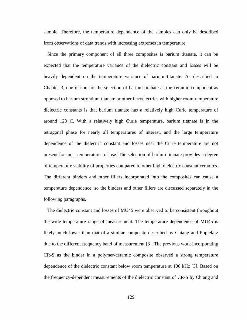
129
sample. Therefore, the temperature dependence of the samples can only be described
from observations of data trends with increasing extremes in temperature.
Since the primary component of all three composites is barium titanate, it can be
expected that the temperature variance of the dielectric constant and losses will be
heavily dependent on the temperature variance of barium titanate. As described in
Chapter 3, one reason for the selection of barium titanate as the ceramic component as
opposed to barium strontium titanate or other ferroelectrics with higher room-temperature
dielectric constants is that barium titanate has a relatively high Curie temperature of
around 120 C. With a relatively high Curie temperature, barium titanate is in the
tetragonal phase for nearly all temperatures of interest, and the large temperature
dependence of the dielectric constant and losses near the Curie temperature are not
present for most temperatures of use. The selection of barium titanate provides a degree
of temperature stability of properties compared to other high dielectric constant ceramics.
The different binders and other fillers incorporated into the composites can cause a
temperature dependence, so the binders and other fillers are discussed separately in the
following paragraphs.
The dielectric constant and losses of MU45 were observed to be consistent throughout
the wide temperature range of measurement. The temperature dependence of MU45 is
likely much lower than that of a similar composite described by Chiang and Popielarz
due to the different frequency band of measurement [3]. The previous work incorporating
CR-S as the binder in a polymer-ceramic composite observed a strong temperature
dependence of the dielectric constant below room temperature at 100 kHz [3]. Based on
the frequency-dependent measurements of the dielectric constant of CR-S by Chiang and

130
Popielarz, 100 kHz is below the relaxation frequency of CR-S. Their data shows that CR-
S exhibits a large decrease in the dielectric constant from approximately 20 at 100 kHz to
between 10 and 15 at 10 MHz [3]. By lowering the material temperature, the frequency-
dependent decrease in the dielectric constant is likely shifted to progressively lower
frequencies, resulting in the observed temperature dependence at 100 kHz. However,
since the temperature-dependent measurements taken in this study were all above this
relaxation frequency, the temperature dependence is not observed between 200 MHz and
4.5 GHz. Although CR-S has a softening temperature of 90-110 C, no polymer flow or
loss that could compromise the mechanical integrity of the composite was observed in
heating the sample to 120 C.
The dielectric constant and losses of MU100 were also consistent throughout the
measured temperature range. This consistency is expected due to the polysilsesquioxane
binder. The polysilsesquioxane binder is non-polar and has a low dielectric constant.
Thus there is a small margin for change in the dielectric constant of the binder and
correspondingly low change in the dielectric constant of the composite. The incorporation
of a temperature-stable ceramic and binder result in stable dielectric properties with
temperature. Since the polysilsesquioxane can withstand very high temperatures, as
described later in this chapter, melting of the polysilsesquioxane is also not an issue.
For MU550, the agar alone is not expected to contribute a strong temperature
dependence due to its non-polar structure and relatively low dielectric constant. The
effects of the liquid filler are substantially more significant. To demonstrate the
temperature dependence of EC50, permittivity measurements were made at room
temperature and above 100 C. To take the high temperature measurement, EC50 was

131
heated to 130 C and removed from the oven. The measurement was taken as the sample
was cooling between 120 C and 100 C. As shown in Figure 37, the dielectric constant of
high temperature EC50 at the lower end of the measured frequency band is significantly
reduced. However, the dispersion of the dielectric constant at high temperature is also
reduced, resulting in the high temperature dielectric constant exceeding the room
temperature dielectric constant above approximately 2.8 GHz. The relatively flat
dielectric constant dependence of the high temperature EC50 is desirable over the very
high dispersion present at room temperature.
Figure 37. Dielectric constant of EC50 at room temperature and greater than 100C
Figure 36 shows the dissipation factor of EC50 at room temperature and above 100 C.
The dissipation factor of the high temperature EC50 is much lower than that of the room
temperature EC50. The high temperature trends of lower dispersion in the dielectric
constant and much lower losses can provide an advantage to using MU550 in a high
temperature application. Although agar has a melting point of approximately 85 C, there

132
was no sign of polymer flow or softening of the composite that would compromise the
mechanical integrity of the composite.
Figure 38. Dissipation factor of EC50 at room temperature and greater than 100C
4.3 Polarization
4.3.1 Polarization Methods
The polarization method facilitates measurement of the dependence of the polarization
on the electric field in the material under test. In ferroelectric materials, the dielectric
constant is drastically reduced above a saturating electric field. Determining the
hysteresis curve for composites containing ferroelectric components can be important to
determine if saturation occurs in the composite. If saturation does occur in the composite,
the maximum operating electric field may be lower than the dielectric strength to
maintain a constant dielectric constant. A second reason for measuring the polarization is
to determine the dielectric constant under high electric field conditions. Although the
frequency of the polarization measurements is lower than the VHF and UHF bands of

133
interest, the high electric field dielectric constant measurements provide information on
the field dependence of the dielectric constant that low voltage network analysis
measurements cannot provide.
The method implemented to measure this relationship is a modification of that used by
Sawyer and Tower in 1930 [4]. The schematic of the circuit is shown in Figure 5. An AC
voltage, VAC, is applied across two capacitors in series. One of the capacitors, CT, is made
with the dielectric material under test, and the other capacitor, C0, has a known
capacitance with negligible dependence on the applied electric field. The resistor, R, can
be included to limit the current from the high voltage transformer. The resistor can be
necessary to limit the current in the secondary circuit for some transformers that will
detect a high current as a fault condition.
Figure 39. Schematic of the modified Sawyer-Tower circuit
Since the charge, Q [C], on the two capacitors in series is distributed equally, analysis of
the voltage across each capacitor results in information on how the polarization changes
versus the electric field. As the voltage of the AC source and the electric field in the
dielectric material of CT varies during each cycle, the voltage distribution between CT and
C0, is dependent upon the dielectric constant of the material under test. By plotting the
variation of the polarization, P [µC/cm2] or [nC/cm
2], versus the electric field, E [MV/m],
in the dielectric material under test, a hysteresis curve is obtained. The hysteresis curve
graphically presents the variation of the dielectric constant with respect to the electric

134
field. To produce the hysteresis curve, the electric field, Eavg [V/m], is calculated as the
voltage across the test capacitor, VT [V], divided by the thickness of the material under
test, tMUT [m]. This calculation is for the average electric field without consideration of
the field effect enhancement at the electrode edges. The charge, Q [C], on each capacitor
can be calculated as the product of the voltage across the known capacitor, V0 [V], and
the capacitance of the known capacitor, C0 [F]. The polarization (C/m2) is calculated as
the stored charge divided by the known area, A [m2] of the electrodes of the capacitor
under test. Using these parameters, the permittivity is calculated by determining the slope
from two points along a linear portion of the polarization-electric field curve. By dividing
the permittivity by the permittivity of free space, the dielectric constant can be calculated.
Equation (4.9) summarizes these calculations and demonstrates how the dielectric
constant can be calculated from two data points of voltage across the known and test
capacitors.
(4.9)
Polarization measurements were made at both low and high applied voltage.
Comparison of the low and high applied voltage measurements provides the most direct
means to examine the dependence of the dielectric constant on the electric field. The low
voltage source was an LCR meter with a 1 V applied signal at 100 Hz. For this low
voltage system, the test leads of the LCR meter were connected directly across the series
arrangement of the known and test capacitors. No series resistance was included in the
circuit, and since a high voltage transformer with a mid-point ground was not included,
one of the test leads was grounded.

135
The high voltage polarization test stand was implemented with a high voltage
transformer that is designed for use with 120 V AC mains power. A variac was used to
adjust the voltage amplitude supplied to the high voltage transformer. At the full mains
amplitude, the high voltage transformer is capable of supplying an RMS voltage of up to
15 kV at 60 Hz. No series resistor was required to limit the current from the high voltage
transformer. The high voltage polarization measurements were conducted in an oil bath
to reduce the likelihood of flashover around the sample surfaces.
The capacitors under test were fabricated with 25.4 mm diameter disks of the
composite material. The thickness of the composites was less than 1.5 mm, and the
surface was sanded and polished to a fine roughness. A platinum electrode with a
diameter of approximately 12 mm was sputtered on each side of the composite to form a
sample capacitor. Conductive silver paste was applied over the platinum electrode to
improve the conductivity of the electrode and to prevent mechanical abrasion of the
platinum layer. A thin layer of CM114-14A high dielectric ink with a dielectric constant
of approximately 40 was applied around the edges of the electrode in an attempt to
minimize the field effect enhancement at the triple point. The sample capacitor was
mounted in an acrylic holder, and brass hardware facilitated electrical contact with the
capacitor electrodes and external connections.
The results from sample capacitors of MU45 and MU100 are presented here. MU550 is
not included due to incompatibility with low frequency measurement methods in its
current form. Due to the inclusion of the polar solvent EC50, mobile ions are present in
the composite. While the antenna frequencies of interest are too high for charge transport
with the ions to occur, low frequency signals do see effects from ion movement. In

136
particular, a double layer can form at the electrode surface, resulting in very high charge
storage that would correspond to dielectric constant values on the order of tens of
thousands to millions. However, the separation of charges is no longer the dielectric
material’s thickness when a double layer is formed. As in the case of ultracapacitors, the
double layer is only stable at voltages that are too low to drive the electrochemical
oxidation and reduction reactions. Higher voltages result in leakage current within the
composite. Therefore, meaningful evaluation of MU550 at low frequency is not possible.
To ensure very little variation of the capacitance of the reference capacitor with respect
to the electric field, the reference capacitors were chosen based on the dielectric
properties. A high voltage mica capacitor rated at 2 nF was used in the measurements of
MU45, and a metalized plastic capacitor measured at 2.48 nF was used in the
measurements of MU100.
4.3.2 Polarization Results
Polarization measurements were taken at low electric fields with an LCR meter source.
The frequency was 100 Hz as it was the closest frequency to the 60 Hz high electric field
source that the LCR meter was capable of producing. Figure 40 shows the hysteresis
curve of the MU45 composite at low electric field levels from the 100 Hz source. The
dielectric constant corresponding to the slope of the polarization-electric field trace is
approximately 109.3. A dashed line in the center of the hysteresis curve with a slope
corresponding to a dielectric constant of 109.3 is included for reference. The dielectric
constant is much greater than 45 due to the lower frequency of the polarization
measurement and the elimination of air gaps by the sputtered electrodes. Due to the low
frequency of the measurement, the dielectric constant of the CR-S binder is much higher

137
than its high frequency value, contributing to the increase in the low voltage dielectric
constant value.
Figure 40. Polarization vs. electric field of MU45 at low electric field levels from a 100
Hz source
Figure 41 shows the hysteresis curve for MU45 measured with the high voltage 60 Hz
source. The slope of the curve does not show any signs of saturation up to 2 MV/m. The
dielectric constant is estimated from the curve to be approximately 208.6. This is nearly
double the value observed from low voltage measurement, suggesting that the effective
dielectric constant of MU45 is significantly higher under high electric field conditions.

138
Figure 41. Polarization vs. electric field for MU45 under high electric field
The same MU45 sample was tested to electric field strengths greater than 6 MV/m. As
shown in Figure 42, there was no sign of ferroelectric saturation. From the hysteresis
curve, the dielectric constant was calculated to be approximately 323.7. This indicates
that the dielectric constant continues to increase due to increases in the maximum electric
field between 2 and 6 MV/m. It is unknown if the measured dielectric constant would
continue to increase at higher electric field levels.
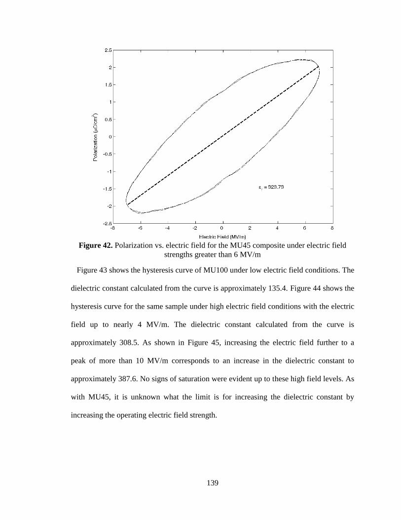
139
Figure 42. Polarization vs. electric field for the MU45 composite under electric field
strengths greater than 6 MV/m
Figure 43 shows the hysteresis curve of MU100 under low electric field conditions. The
dielectric constant calculated from the curve is approximately 135.4. Figure 44 shows the
hysteresis curve for the same sample under high electric field conditions with the electric
field up to nearly 4 MV/m. The dielectric constant calculated from the curve is
approximately 308.5. As shown in Figure 45, increasing the electric field further to a
peak of more than 10 MV/m corresponds to an increase in the dielectric constant to
approximately 387.6. No signs of saturation were evident up to these high field levels. As
with MU45, it is unknown what the limit is for increasing the dielectric constant by
increasing the operating electric field strength.

140
Figure 43. Polarization of MU100 under low electric field conditions
Figure 44. Polarization of MU100 under high electric field conditions up to nearly 4
MV/m
141
Figure 45. Polarization of MU100 under high electric field conditions up to more than 10
MV/m
4.4 Capacitive Discharge
4.4.1 Capacitive Discharge Methods
A second high voltage diagnostic method in addition to the polarization measurements
was implemented in the form of a high voltage capacitive discharge test stand. The high
voltage capacitive discharge test stand was used to record the discharge waveform of
small capacitors formed with the composite materials into a known resistance. Post-
processing of the data enabled the dielectric constant of the material to be estimated while
under high voltage conditions. While the frequencies present in the capacitor discharge
waveform were generally lower than the application antenna frequencies, the capacitive
discharge data provided additional information on the observed increase in the dielectric
constant under high voltage conditions.

142
Figure 46 shows the schematic of the high voltage capacitive discharge test stand. A
negative polarity high voltage power supply, VDC, charged the capacitor under test, C,
through a charging resistor, RC. A mechanical safety switch, SD, was open during
charging but was available to dump the charge through resistor RD. A high voltage IGBT
switch stack, SL, was closed after charging is complete to discharge the capacitor through
the load resistor, RL.
Figure 46. Schematic of the High Voltage Capacitive Discharge Test Stand
The charging voltage was monitored with a Fluke 80K-40 1000:1 voltage probe. The
fast discharge of the capacitor was monitored with a Northstar PVM6 1000:1 high
voltage probe. The discharge was recorded on a Tektronix TDS 5054B oscilloscope. A
custom Matlab program generated a fit to the discharge curve, enabling calculation of the
capacitance and effective dielectric constant. Non-inductive resistors were used for the
load resistor with values ranging from 1 Ω to 105 kΩ. Figure 47 shows the custom high
voltage capacitive discharge test stand.
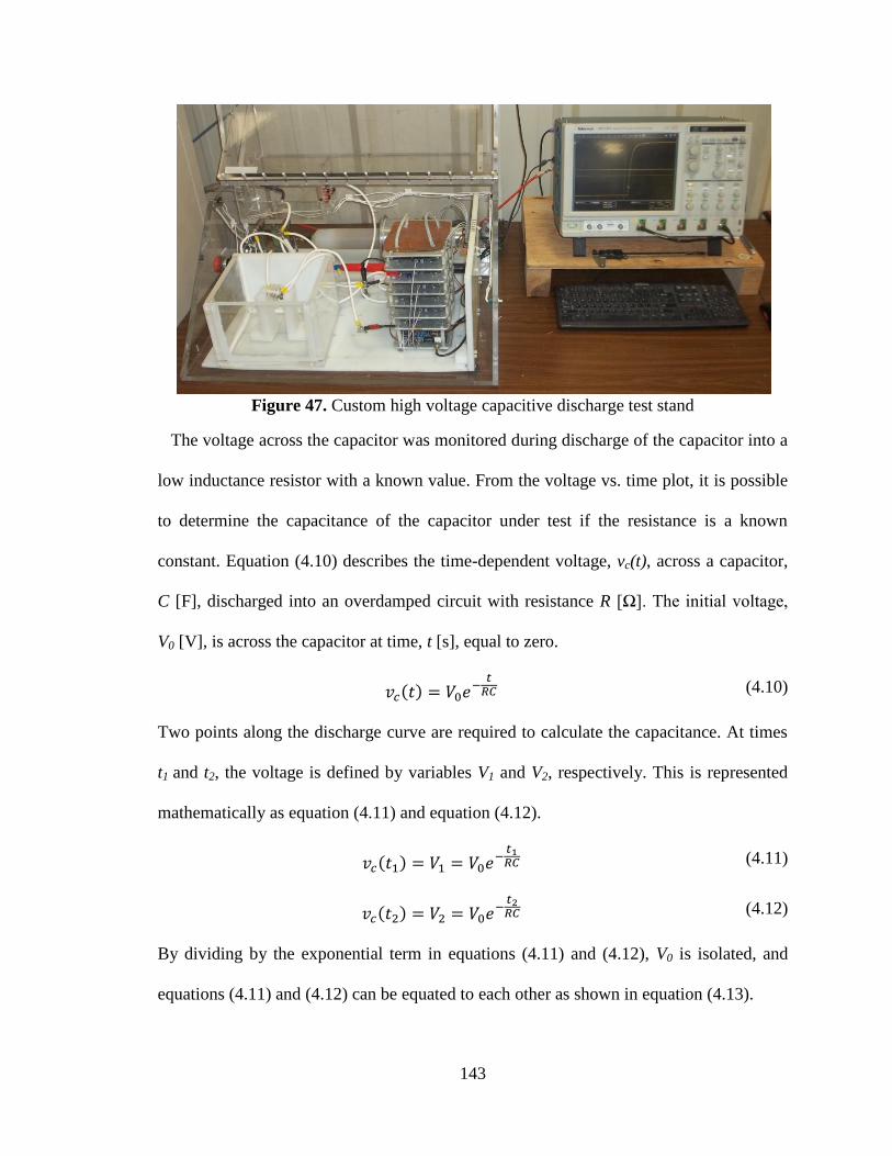
143
Figure 47. Custom high voltage capacitive discharge test stand
The voltage across the capacitor was monitored during discharge of the capacitor into a
low inductance resistor with a known value. From the voltage vs. time plot, it is possible
to determine the capacitance of the capacitor under test if the resistance is a known
constant. Equation (4.10) describes the time-dependent voltage, vc(t), across a capacitor,
C [F], discharged into an overdamped circuit with resistance R [Ω]. The initial voltage,
V0 [V], is across the capacitor at time, t [s], equal to zero.
(4.10)
Two points along the discharge curve are required to calculate the capacitance. At times
t1 and t2, the voltage is defined by variables V1 and V2, respectively. This is represented
mathematically as equation (4.11) and equation (4.12).
(4.11)
(4.12)
By dividing by the exponential term in equations (4.11) and (4.12), V0 is isolated, and
equations (4.11) and (4.12) can be equated to each other as shown in equation (4.13).

144
(4.13)
The unknown capacitance can be defined based on the two time and voltage points from
the discharge waveform and the known resistance as given by equation (4.14).
(4.14)
The effective dielectric constant of the materials was calculated based on the simple
equation for a parallel-plate capacitor as shown in equation (4.15). The effect of the
fringe fields was ignored as is common in practice as the additional capacitance obtained
from fringe fields when measuring a high dielectric constant material are relatively small.
In equation (4.15), εr is the effective dielectric constant of the composite material, and C
[F] is the calculated capacitance. The material thickness is again tMUT [m], and A [m2] is
the area of the capacitor electrodes.
(4.15)
Samples of MU45 and MU100 were prepared as described in the previous subsection
with electrodes consisting of sputtered platinum covered with a silver epoxy paste. The
measurements were conducted in atmospheric air as opposed to the oil environment used
in the polarization measurements.
4.4.2 Capacitive Discharge Results
Figure 48 displays the voltage discharge waveform obtained when discharging a small
capacitor made with MU45 from a voltage of approximately -2 kV. The capacitor had
electrodes with a diameter of approximately 12 mm, and the thickness of the MU45
material was approximately 1.13 mm. The load resistance was measured to be

145
approximately 10.4 kΩ. Two empty circles indicate the points along the discharge curve
at which the time and voltage was sampled for calculation of the capacitance. From these
points, the capacitance was calculated to be 177.1 pF, corresponding to an effective
dielectric constant of MU45 of approximately 199.8. For a voltage magnitude of 2 kV
and a thickness of 1.13 mm, the average electric field in the composite was
approximately 1.77 MV/m. The dielectric constant of 199.8 observed through capacitive
discharge with a peak field of 1.77 MV/m agrees very well with the dielectric constant of
208.6 of Figure 41 obtained through polarization measurements at a peak field of slightly
more than 2 MV/m. These two measurement methods produced very close dielectric
constant measurements at similar peak field strengths. However, it should be noted that
the dielectric constant obtained from high voltage discharges of MU45 at higher voltages
were also consistently around 200. The dielectric constant calculated from those
capacitive discharges did not increase to the same levels observed from very high electric
field polarization measurements as in Figure 42.
Figure 48. Discharge waveform of a capacitor made with MU45

146
Figure 49 shows a waveform of a capacitor made from MU100 discharged from
approximately -2 kV. The sample capacitor had an electrode diameter of approximately
12 mm and a thickness of approximately 1.27 mm. The load resistance was again 10.4
kΩ. The capacitance calculated from the discharge curve was 272.27 pF, and the
corresponding effective dielectric constant was approximately 345.3. Although this
capacitive discharge had a lower peak electric field magnitude, the calculated dielectric
constant fits between the values obtained at high electric field through polarization
measurements as shown in Figure 44 and Figure 45. Different samples of MU100 were
used in the polarization measurement and the high voltage capacitive discharge
measurement, but the effective dielectric constant at high voltage is similar between
samples and measurement methods. As noted for MU45 capacitive discharge
measurements, the effective dielectric constants observed for MU100 in capacitive
discharge measurements were similar for multiple charge voltage magnitudes, and the
dielectric constant did not continue to increase with increasing peak electric field as it did
in polarization measurements.
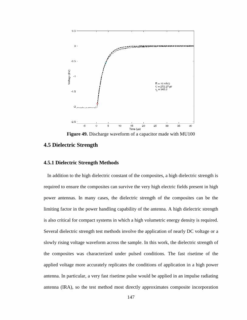
147
Figure 49. Discharge waveform of a capacitor made with MU100
4.5 Dielectric Strength
4.5.1 Dielectric Strength Methods
In addition to the high dielectric constant of the composites, a high dielectric strength is
required to ensure the composites can survive the very high electric fields present in high
power antennas. In many cases, the dielectric strength of the composites can be the
limiting factor in the power handling capability of the antenna. A high dielectric strength
is also critical for compact systems in which a high volumetric energy density is required.
Several dielectric strength test methods involve the application of nearly DC voltage or a
slowly rising voltage waveform across the sample. In this work, the dielectric strength of
the composites was characterized under pulsed conditions. The fast risetime of the
applied voltage more accurately replicates the conditions of application in a high power
antenna. In particular, a very fast risetime pulse would be applied in an impulse radiating
antenna (IRA), so the test method most directly approximates composite incorporation
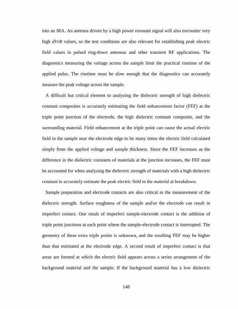
148
into an IRA. An antenna driven by a high power resonant signal will also encounter very
high dV/dt values, so the test conditions are also relevant for establishing peak electric
field values in pulsed ring-down antennas and other transient RF applications. The
diagnostics measuring the voltage across the sample limit the practical risetime of the
applied pulse. The risetime must be slow enough that the diagnostics can accurately
measure the peak voltage across the sample.
A difficult but critical element to analyzing the dielectric strength of high dielectric
constant composites is accurately estimating the field enhancement factor (FEF) at the
triple point junction of the electrode, the high dielectric constant composite, and the
surrounding material. Field enhancement at the triple point can cause the actual electric
field in the sample near the electrode edge to be many times the electric field calculated
simply from the applied voltage and sample thickness. Since the FEF increases as the
difference in the dielectric constants of materials at the junction increases, the FEF must
be accounted for when analyzing the dielectric strength of materials with a high dielectric
constant to accurately estimate the peak electric field in the material at breakdown.
Sample preparation and electrode contacts are also critical to the measurement of the
dielectric strength. Surface roughness of the sample and/or the electrode can result in
imperfect contact. One result of imperfect sample-electrode contact is the addition of
triple point junctions at each point where the sample-electrode contact is interrupted. The
geometry of these extra triple points is unknown, and the resulting FEF may be higher
than that estimated at the electrode edge. A second result of imperfect contact is that
areas are formed at which the electric field appears across a series arrangement of the
background material and the sample. If the background material has a low dielectric

149
constant in comparison with the material under test, the majority of the electric field will
be present in the background material. Breakdown of the background material can
contribute to premature breakdown of the sample through effects such as heating and
surface ionization from electrons accelerated in the background material.
Based on the field enhancement concerns discussed in the preceding paragraphs, efforts
were made to provide a uniform electrode contact and to account for the FEF at the
electrode edge. The samples were prepared with extensive sanding and polishing to
prepare the surface to a very fine surface roughness. To further improve the sample-
electrode contact, the electrodes were applied directly to the sample. As shown in Figure
50, platinum electrodes were sputtered directly onto the sample surfaces. The sputtering
masks were prepared to ensure that the electrodes on opposite surfaces were directly
adjacent from each other. To prevent mechanical abrasion of the sputtered electrodes and
to improve electrode conductivity, a silver-loaded epoxy was applied to the sputtered
electrodes. With the electrodes in place on the sample surface, the external electrical
contacts applied to the silver-loaded epoxy theoretically should not influence the electric
field within the sample. Therefore, electrode surface pitting on the external contacts does
not affect the sample-electrode contact. To further ensure that surface pitting does not
influence the electrical contact between the external circuit and the silver-loaded epoxy,
the external contacts were fitted with replaceable tips in the form of acorn nuts. As shown
in Figure 51, the electrode tips were replaced after every three samples to prevent
excessive wear from pitting.

150
Figure 50. Samples prepared for dielectric strength testing. From left to right in sets of
six: MU45, MU100, and MU550
Figure 51. Dielectric strength test cell
Figure 52 shows the circuit of the dielectric strength test stand. A PA-80 pulse
generator from L-3 Communications Pulse Sciences was implemented as the high voltage
source of the dielectric strength test stand [5]. A 75 nF capacitance, CS, is resistively
charged to between -60 kV and -80 kV from a DC supply. After charging, the switch, S,
is triggered by a PT-55, discharging the capacitor into the transmission line, T. Since the
capacitor electrode that is initially negatively charged with respect to ground is grounded
through switch S, the polarity of the pulse on the transmission line is positive. The
151
transmission line is a 50 Ω cable of RG-218/U. The transmission line is terminated into a
load consisting of a parallel arrangement of the dielectric test cell, a capacitance, C1, of
0.54 nF, and a resistance, R1. Since C1 is much smaller than CS, the voltage across the
sample can reach a peak up to nearly two times VDC if no breakdown in the sample
occurs. In normal operation, the value of R1 is reduced to between 50 and 100 Ω to limit
the peak voltage across the test cell to less than 100 kV to prevent damage to the voltage
diagnostics. The voltage diagnostics were two PVM-6 high voltage probes monitoring the
voltage on each side of the sample under test. The maximum recommended frequency of
the PVM-6 is 80 MHz, corresponding to a risetime of between 4 and 5 ns.
Figure 52. Circuit schematic of pulsed dielectric strength test stand
Figure 53 shows example waveforms recorded during dielectric strength testing. The
voltage waveforms were measured from both sides of the dielectric sample. Figure 54
displays the voltage across the dielectric sample. In this example, a peak voltage of nearly
70 kV was applied across the sample before dielectric breakdown. The 10%-90%
risetime of Figure 54 is approximately 85 ns.

152
Figure 53. Example voltage waveforms from both sides of test cell
Figure 54. Pulsed voltage across a dielectric sample showing the risetime of the applied
voltage

153
Figure 55 shows the PA-80, transmission line load, and diagnostic arrangement. The
experiments were conducted in an oil bath to prevent flashover or arcing around the
sample under test.
Figure 55. The PA-80 pulse generator with test cell and diagnostics
Six samples of MU45, MU100, and MU550 were prepared as previously described for
dielectric strength testing. Each sample had four measurement sites prepared on it by the
application of sputtered platinum electrodes covered with a silver-loaded epoxy for a total
of twenty-four potential data points for each class. In addition to the three high dielectric
constant composite classes, six Teflon samples with four measurement sites each were
also tested for comparison. Of the three classes of high dielectric constant composites,
three samples were tested without a high dielectric constant coating around the electrode
edge. Three samples were prepared with a coating of CM114-14A high dielectric

154
constant ink, which has a dielectric constant of 40, around the electrode edge in an
attempt to reduce the FEF at the triple point junction. Since Teflon has a relatively low
dielectric constant of approximately 2.08, the application of the high dielectric constant
ink would have increased the FEF on those samples. Therefore, no Teflon samples were
coated with the high dielectric constant ink.
The thickness at each measurement site was measured after the platinum electrodes
were sputtered onto the surface but before application of the silver-loaded epoxy. The
FEF was estimated through electrostatic simulation in Maxwell SV. A simulation was run
for each data point with a unique thickness. The FEF was calculated as the ratio of the
peak simulated field to the average field calculated as the applied voltage divided by the
thickness at the test site. The high frequency dielectric constants measured through
network analysis of 45, 100, and 550 were used in the simulation of each respective
composite class. For the dielectric constant of Teflon, the value stored in Maxwell SV of
2.08 was used. The background material was simulated as oil with a dielectric constant of
2.2, and the high dielectric constant coating had a simulated value of 40. To determine
the geometry of the electrode edge interface with the composite, the junction was
examined through scanning electron micrographs. Figure 56 shows two electrode edges
formed from the application of a silver-loaded epoxy over the sputtered platinum contact.
These samples were prepared by fracturing the sample to provide a cross-sectional view
of the electrode-composite junction. The micrographs shows a good contact along the
junction, and the high loading factor of silver particles within the epoxy is evident. The
thickness of the electrode gradually decreases towards the electrode edge, forming a
curvature with a radius of approximately 100 µm.

155
Figure 56. Micrograph of electrode-composite edges
The electrode edge geometry observed in Figure 56 with a radius of curvature of 100 µm
was implemented in the simulations of the FEF for each data sample. Figure 57 provides
an example of the simulated structure from Maxwell SV showing the 100 µm thick
electrodes on a sample with a dielectric constant of 100. The electrodes are colored red
and feature the curvature at the edge with a radius of 100 µm. In this example, the peak
electric field at the triple point was 10.16 MV/m. The field in the bulk of the material to
the left of Figure 57 is 1.22 MV/m, so the FEF in this simulation was 8.33.
Figure 57. Electrode geometry simulated in Maxwell SV for estimation of the field
enhancement factor

156
Estimating the FEF from electrostatic simulations has some disadvantages. In
particular, the peak electric field value is highly dependent on the density of the mesh
generated for each simulation. To limit the effects of variations due to mesh density, all
of the FEF values were calculated under the same simulation settings. The accuracy of
the simulations was run to less than 0.5% error in the energy calculation.
The dielectric strength data is evaluated with the Weibull distribution, which is
commonly applied in failure analysis [6]. The cumulative distribution function, F,
adapted to this analysis is given as equation (4.16), where Epeak is the calculated peak
electric field at breakdown, λW is the Weibull scale parameter, and kW is the Weibull
shape parameter.
(4.16)
When equation (4.16) is rearranged to the form of equation (4.17), the distribution
function can be plotted as a straight line.
(4.17)
A Weibull plot compares the experimental data to a straight line described by equation
(4.17). The Weibull parameters kW and λW can be determined if the data fits to a line
described by equation (4.17).
4.5.2 Dielectric Strength Results
The first data set contains the samples without a high dielectric constant coating around
the electrode edge. In this data set, the number of data samples for MU45, MU100,
MU550, and Teflon number 10, 10, 9, and 23. Of the 12 test sites prepared without a high
dielectric constant coating for the MU45, MU100, and MU550 composites and the 24 test

157
sites prepared for Teflon, the number of data samples for analysis is lower for one of two
reasons. First, if a prior data sample caused a fracture in the composite that extended to
the electrode edge of another sample, data was not taken on the compromised sample.
Second, in rare instances, diagnostic or data collection problems resulted in the loss of a
data point.
Figure 58 displays the Weibull plot of samples without a high dielectric constant
coating and without inclusion of the field enhancement factor. The field enhancement
factor is not included in this first plot to examine if the data initially fits a Weibull
distribution before inclusion of triple point effects. The quoted electric fields are the
values present in the bulk of the material and are referred to as the average field. The
average field varies from 18.8 to 41.8 MV/m for MU45, 45.3 to 51.7 MV/m for MU100,
33.5 to 41.6 MV/m for MU550, and 93.7 to 137 MV/m for Teflon. Table 5 summarizes
the Weibull parameters calculated through data analysis in Matlab. The data for MU100,
MU550, and Teflon appear to fit the straight line very well. The data for MU45 has the
worst fit. It is possible that due to the higher polymer content in MU45, variation in the
dispersion and packing density of the particles at different points in the composite is
greater than MU100 and MU550, which have lower polymer content. The higher degree
of variation found in MU45 could effectively produce an inhomogeneous medium that
would not exhibit dielectric strength data with a good fit to the Weibull distribution.

158
Figure 58. Weibull plot of electric field at breakdown without a dielectric coating and
without inclusion of the field enhancement factor
Table 5. Summary of Weibull Parameters for Samples without Coating and without FEF
Included
MU45 MU100 MU550 Teflon
Number of Samples 10 10 9 23
kW -Shape
Parameter 3.48 21.5 14.35 9.05
λW - Scale Parameter 26.88 48.1 37.68 116.15
Table 6 summarizes the data for samples without a high dielectric constant coating and
without consideration of the field enhancement factor. The relatively large amount of
variability in the breakdown data obtained for MU45 results in a significantly lower
electric field at 1% probability of breakdown than MU100 and MU550. MU100 and
MU550 showed relatively low variation in the electric field at breakdown in the bulk of
the material with both composites’ values falling within a range of ±5 MV/m from the
median value. Teflon exhibited the highest range of electric fields when the field

159
enhancement factor is not considered. This is expected due to the relatively low field
enhancement factor of Teflon in comparison to the high dielectric constant composites.
Table 6. Summary of electric field data for samples without a high dielectric constant
coating and without inclusion of the field enhancement factor
MU45 MU100 MU550 Teflon
Max Electric Field (MV/m) 41.76 51.73 41.62 137
Min Electric Field (MV/m) 18.82 45.27 33.5 93.7
Electric Field at 1% Probability of
Breakdown (MV/m) 7.17 38.84 27.35 69.87
Figure 59 shows a plot of the same data set that produced Figure 58 without a high
dielectric constant electrode coating but with inclusion of the field enhancement factor.
Including the FEF, the peak field measurements vary from 165.4 to 308.54 MV/m for
MU45, 358.76 to 501.32 MV/m for MU100, 276.87 to 419.87 MV/m for MU550, and
259.28 to 379.11 MV/m for Teflon. Inclusion of the field enhancement factor decreased
the quality of the fit to a Weibull distribution. This is partially due to the limitations of
estimating the field enhancement factor of each sample with electrostatic simulations.
Despite the variance that can occur between electrostatic simulations, the FEFs calculated
from these simulations provide the best estimate at the actual FEF and give insight to the
peak fields present at the electrode edges.

160
Figure 59. Weibull plot of electric field at breakdown without a high dielectric constant
coating and with the field enhancement factor
Table 7. Summary of Weibull parameters for samples without a coating and with FEF
included
MU45 MU100 MU550 Teflon
Number of Samples 10 10 9 23
kW -Shape
Parameter 4.71 11.44 5.48 9.05
λW - Scale Parameter 228.05 473.21 405.31 321.39
Table 8 summarizes the electric field data at breakdown. The FEF is much higher for the
composites than for Teflon due to the dependence of the FEF on the dielectric constant of
the materials. When accounting for the FEF, the peak electric field at breakdown was
higher in MU100 than in Teflon. As seen in Figure 59, many of the data points for
MU550 with the FEF included were higher than those for Teflon. However, due to the
slope of the line fit to the data in the Weibull analysis, the value at 1% probability of
breakdown is slightly lower for MU550 than for Teflon. To effectively utilize the high

161
dielectric strength of the composites, the FEF must be lowered such that the average
electric field is not significantly lower than the peak field. As theoretically demonstrated
in the simulations described in Chapter 3, one way to potentially lower the FEF to levels
at which the average field can be significantly raised is to coat the triple point at the
electrode edge with a high dielectric constant material.
Table 8. Summary of electric field values for samples without coating and with FEF
MU45 MU100 MU550 Teflon
Average Simulated Field Enhancement
Factor 8.80 9.60 9.49 2.77
Max Electric Field (MV/m) 308.54 501.32 419.87 379.11
Min Electric Field (MV/m) 165.40 358.76 276.87 259.28
Electric Field at 1% Probability of
Breakdown (MV/m) 85.87 316.53 175.07 193.32
Figure 60 shows the Weibull plot of dielectric strength data for MU45 and MU100 with
an electrode coating of a high dielectric constant ink. While the FEF is predicted to be
reduced to 1.95 and 2.21 for MU45 and MU100, respectively, the FEF is not included in
the plot of Figure 60 and the data of Table 9 and Table 10 to enable direct comparison
with the average electric values previously presented for samples without a coating. Data
for MU550 was unavailable for this coating due to incompatibility of the binder in the
high dielectric constant ink with the EC50 component of MU550. The same technique
could be applied to MU550 with a high dielectric constant coating that is insoluble in
EC50. A total of 12 data points were available for MU45, and 7 data points were obtained
for MU100. Table 9 summarizes the Weibull parameters for this data set with a high
dielectric constant electrode coating.

162
Figure 60. Weibull plot of electric field at breakdown for MU45 and MU100 samples
with high dielectric constant coating around electrode edges but without FEF
Table 9. Summary of Weibull parameters for samples with coating but without FEF
MU45 MU100
Number of Samples 12 7
kW -Shape Parameter 3.2 9.29
λW - Scale Parameter 28.33 55.64
Table 10 summarizes the electric field values observed and calculated from the Weibull
analysis. If the coating effectively reduced the FEF to 1.95 and 2.21 for MU45 and
MU100, respectively, the electric field observed at breakdown should increase by an
average factor of between 4 and 4.5. However, the observed values suggest the coating
had either no effect or a somewhat negative. The electric fields at 1% probability of
breakdown for the cases with and without the coating are reduced by 6.14% and 12.7%
for MU45 and MU100, respectively.

163
Table 10. Summary of Electric Field Values for Samples with Coating without FEF
MU45 MU100
Max Electric Field (MV/m) 45.20 63.72
Min Electric Field (MV/m) 14.96 45.19
Electric Field at 1% Probability of Breakdown (MV/m) 6.73 33.91
There are three possibilities that could explain why the coating did not produce the
desired effect. The first possibility is that the high dielectric constant coating did not
thoroughly coat the triple point junction. This could be due to poor compatibility between
the coating and surfaces of the electrode and/or composite, too high viscosity of the
coating, trapped gas within the coating, or other factors. The second possibility is that the
breakdown was dominated by triple points along the electrode-composite junction away
from the edges. The third possibility is that dielectric breakdown in dominated by field
concentration with the composite, and effects at the electrode-composite junction do not
factor into the dielectric strength. Assuming the FEF due to the electrode-composite
junction at the edges does impact the dielectric strength, a larger study is required to
develop methods to effectively reduce the FEF. To better implement a high dielectric
constant electrode coating, the study must examine issues such as the wettability of the
coating to the composite surface, the viscosity of the coating to flow into small features
along the electrode edge, the size of filler particles within the coating, and the elimination
of gas from the coating.
4.6 Thermogravimetric Analysis
4.6.1 Thermogravimetric Analysis Methods
Thermogravimetric analysis refers to the analysis of the change of a material’s mass
due to changes in temperature. The technique is often used to generate a continuous curve
164
of the sample mass as a function of increasing temperature [7]. Identification of mass loss
at certain temperatures can provide information on the composition of the sample and the
physical processes occurring at particular temperatures [7]. In this work, the analysis was
aimed at determining the weight percentage of binder in each of the composite classes.
This analysis did not require continuous monitoring of the sample mass as the
temperature was raised and lowered. Instead, the sample’s mass was determined before
and after heat treatment.
One sample of each composite class was prepared for thermogravimetric analysis. The
samples were sanded to limit any error that unevenness in the sample thickness would
contribute to the calculation of the sample volume. The samples were heated at low
temperature for over 24 hours before measurements were taken in an effort to limit the
effect of absorbed water from atmospheric exposure on the mass measurement. The
thickness, diameter, and mass of each sample were measured before the high temperature
treatment. Based on these measurements, the volume and mass density were calculated.
For MU550, the mass was measured both dry and after soaking in EC50. Based on the
difference in the dry and soaked mass and the density of EC50, the weight and volume
percentage of EC50 was calculated. The masses of the composites were measured again
after the high temperature treatment. The difference in masses before and after the heat
treatment along with information about the binder density and ash content permitted
calculation of the remaining parameters of interest.
To determine the ash content of the binders, samples of CR-S, polysilsesquioxane, and
agar were included separately during the same high temperature treatment as the
composites. The masses of the binders were measured before and after the heat treatment.

165
The percentage of the initial binder mass remaining after the high temperature treatment
was considered the ash content, and this percentage of the binder was assumed to have
remained in the composites as well.
Three additional assumptions were required to complete the analysis. First, it was
assumed that none of the ceramic mass was lost during the heat treatment. This is a safe
assumption due to the temperatures in excess of 1000 C at which barium titanate is
routinely processed. The second assumption was that the EC50 soaked into the MU550
sample filled all of the composite’s voids. This assumption was necessary due to the
unknown mass density and volume of the agar in the composite. While this assumption
represents the ideal case and some voids likely remained, the results presented in the
following subsection suggest that the assumption is a reasonable approximation.
Similarly, the third assumption assumes that the polysilsesquioxane binder of MU100
completely fills the voids between the ceramic particles. This assumption was also due to
the unknown mass density and undetermined volume of the polysilsesquioxane. Limited
data is available on the mass density of polysilsesquioxanes, and it is believed that the
porosity and resulting density of the polysilsesquioxane is dependent on the conditions
under which the network forms. In measurement of the mass density from a
polysilsesquioxane formed over a long period of time at room temperature and
atmospheric pressure, the resulting mass density was so low that the predicted volume of
the binder in the composite would have been larger than the composite. The assumption
is considered reasonable as the mass density estimated from the calculations is close to
the mass density of similar polymers, such as polydimethylsiloxane.

166
The high temperature treatment was conducted in an ashing furnace. The temperature
was increased from room temperature to 400 C at a ramp rate of 10 C/min. The furnace
was held at 400 C for 2 hours after which the furnace cooled to room temperature at an
unspecified rate.
4.6.2 Thermogravimetric Analysis Results
The results of the thermogravimetric analysis of the binders are summarized in Table
11. As seen in the estimates of the percentage of ash from each binder, more than 83% of
the CR-S and more than 87% of the agar masses were lost upon heat treatment, but less
than 12% of the polysilsesquioxane was lost. The high remaining amount of PSSQ is due
to the low organic content and high thermal stability of the binder used in MU100. The
estimated binder densities for the PSSQ and agar were calculated from the estimated
mass and volume of the respective binders described later in this section. The estimated
density of the CR-S was obtained from data in the literature for pullulan, and this density
value was used to calculate the estimated volume occupied by the CR-S in MU45 [8].
Table 11. Summary of mass loss from each binder
Mass Before
Burn (g)
Mass After
Burn (g)
Percentage Ash
of Binder
Est. Binder
Density (g/cm3)
CR-S 1.6200 0.0809 16.18% 1.70 [8]
PSSQ 3.1220 1.7747 88.31% 1.40
Agar 1.2539 0.0214 12.52% 0.85
Table 12 provides a summary of the basic measurements of the composites including
the thickness, diameter, and mass before burning. The order of highest to lowest mass
density of the composites before heat treatment was MU100, MU550, and MU45. More
than 1 g, approximately 13% of the composite mass, was lost upon heat treatment of the
MU45 sample.

167
Table 12. Basic properties of the samples analyzed through thermogravimetric analysis
Thickness (mm) Diameter (mm) Composite Volume (cm3)
MU45 4.05 25.16 2.01
MU100 0.82 25.4 0.42
MU550 2.6 25.4 1.32
Mass of
Composite (g)
Composite Density
(g/cm3)
Mass of Binder Lost on
Burning (g)
MU45 7.8327 3.8900 1.0158
MU100 1.9581 4.7126 0.0192
MU550 5.4369 4.1269 0.1636
Table 13 summarizes data on the binder content of the composites. The estimated total
binder mass was determined from the binder lost during heat treatment of the composites
and the percentage ash content observed from the binder alone. The mass percentage was
then calculated directly from the binder and composite masses. The estimated volume of
the binder was calculated from the mass and density of CR-S for MU45. The volume of
MU100 was calculated as the remaining volume unoccupied by the ceramic based on the
assumption that the PSSQ filled all of the voids between ceramic particles. The volume
of agar in MU550 was calculated as the remaining volume unoccupied after accounting
for the volume occupied by the ceramic and EC50. The percentage mass and percentage
volume of binder are important results of this analysis. Unsurprisingly due to the lower
dielectric constant of MU45, the binder content of MU45 is the highest of the three
composites. MU550 had the lowest calculated mass and volume of binder as the agar is
intentionally dried from its swelled state during composite formation, reducing its mass
through water removal.

168
Table 13. Summary of binder content of composites
Est. Total
Binder Mass (g)
Est.
Percentage
Mass of Binder
Est. Volume
of Binder
(cm3)
Est.
Percentage
Volume of
Binder
MU45 1.2119 15.47 0.7129 35.40%
MU100 0.1642 8.39 0.1175 28.28%
MU550 0.1870 3.44 0.2202 16.72%
Table 14 summarizes the ceramic content in each composite class. For MU45 and
MU100, the mass of ceramic was calculated based on the total composite mass and the
binder mass of Table 13. With the ceramic mass established, the ceramic volume is
calculated based on a mass density for barium titanate of 6.02 g/cm3. MU100 had the
highest mass and volume percentage of ceramic followed by MU550 and MU45. The
volume percentage of ceramic for MU100 was estimated to be 71.72%, which is only
about 5% lower than the measured volume percentage obtained with a trimodal mixture
with no binder. All three composite classes have an estimated volume percentage of
ceramic greater than 50%, which is due to the high packing density made possible by
multimodal ceramic particle sizes. The lower volume percentage of ceramic in MU550
and MU45 is attributed to the larger size of the polymers used in those composites and
the polymerization of the binder prior to formation of the composite.
Table 14. Summary of ceramic content of composites
Est. Mass of
Ceramic (g)
Est. Mass
Percentage of
Ceramic
Est. Volume
of Ceramic
(cm3)
Est. Volume
Percentage of
Ceramic
MU45 6.6208 84.53% 1.10 54.62%
MU100 1.7939 91.61% 0.30 71.72%
MU550 4.8944 90.02% 0.81 61.71%
Table 15 provides data on the volume percentage of voids for each composite class.
The volume percentage calculated for MU45, approximately 10%, was calculated as the
remaining volume after accounting for the ceramic and binder. As previously discussed,

169
it was assumed that the PSSQ completely fills the voids of MU100. This assumption is
necessary because the volume occupied by the PSSQ cannot be calculated due to the
unknown density of the PSSQ. Thus the volume percentage is assumed to be the ideal
case of 0%. The volume percentage of voids for MU550 is actually the volume
percentage occupied by EC50 based on the assumption that EC50 completely fills the
composites voids.
Table 15. Summary of void estimates
Estimated Volume Percentage of Voids
(cm3)
MU45 9.98%
MU100 0%
MU550 21.575
Table 16 summarizes how the volume percentage of 21.57% was determined for the
EC50. Based on the measured mass gain upon soaking the previously dried MU550 in
EC50, the volume was calculated with the known mass density of EC50 of 1.251 g/cm3.
Although the volume percentage of voids in MU550 seems high, this volume is filled
with a high dielectric constant material, resulting in the highest high frequency dielectric
constant values of the three composite classes.
Table 16. Summary of EC50 content of MU550
Mass of
EC50 (g)
Percentage Mass
of EC50
Volume of
EC50 (cm3)
Percentage
Volume of EC50
MU550 0.3555 6.54 28.42 21.57
4.7 Scanning Electron Microscopy
4.7.1 Scanning Electron Microscopy Methods
The primary use of scanning electron microscopy (SEM) was to characterize the
ceramic particle size and morphology. Since the ceramic particles were obtained

170
commercially, the suitability of the particles for the intended use had to be verified. In
particular, the large particles and nanoparticles required inspection before use. The large
particles were often initially received as very porous pieces of material. Since the large
particles would only be effective at contributing towards a high volume fraction of
ceramic in the composite if they were non-porous, the SEM analysis revealed that the
large particles could not be used as received but rather needed to be further densified
through a sintering process. The as-received nanoparticles were revealed to often form
large spherical agglomerates. The agglomerates, often measuring several tens of microns
in diameter, also were very porous and of low density. Although the primary particles
forming the agglomerate were at the size scale rated by the manufacturer, the primary
particles could not be adequately mixed into the trimodal composition while in the form
of large agglomerates. SEM analysis revealed the agglomerated nature of the
nanoparticles, and the nanoparticles were imaged again after a milling and chemical
treatment was applied to reduce the agglomerates.
Energy-dispersive X-ray spectroscopy (EDS) was also conducted on some particles and
composites to determine the atomic content of the sample. The EDS analysis provided a
means of verifying the composition of the particles, and spectral mapping enabled a
visual representation of the distribution of elements throughout the surface of the
composites.
Scanning electron microscopy produces images at magnification levels greater than
conventional light microscopy by directing an electron beam with a small spot size across
the sample and detecting the scattered electron and x-ray products of the interaction of
the electron beam and material being imaged. The electron beam is scanned across the
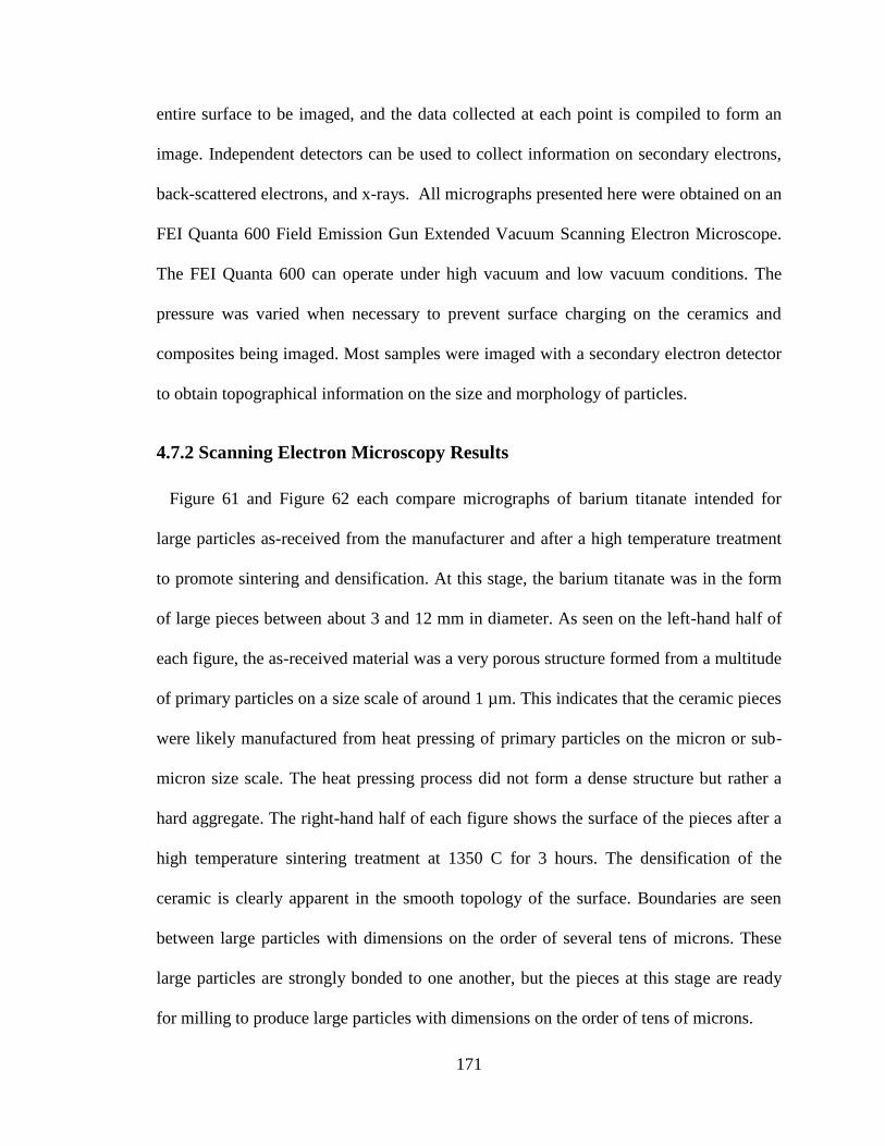
171
entire surface to be imaged, and the data collected at each point is compiled to form an
image. Independent detectors can be used to collect information on secondary electrons,
back-scattered electrons, and x-rays. All micrographs presented here were obtained on an
FEI Quanta 600 Field Emission Gun Extended Vacuum Scanning Electron Microscope.
The FEI Quanta 600 can operate under high vacuum and low vacuum conditions. The
pressure was varied when necessary to prevent surface charging on the ceramics and
composites being imaged. Most samples were imaged with a secondary electron detector
to obtain topographical information on the size and morphology of particles.
4.7.2 Scanning Electron Microscopy Results
Figure 61 and Figure 62 each compare micrographs of barium titanate intended for
large particles as-received from the manufacturer and after a high temperature treatment
to promote sintering and densification. At this stage, the barium titanate was in the form
of large pieces between about 3 and 12 mm in diameter. As seen on the left-hand half of
each figure, the as-received material was a very porous structure formed from a multitude
of primary particles on a size scale of around 1 µm. This indicates that the ceramic pieces
were likely manufactured from heat pressing of primary particles on the micron or sub-
micron size scale. The heat pressing process did not form a dense structure but rather a
hard aggregate. The right-hand half of each figure shows the surface of the pieces after a
high temperature sintering treatment at 1350 C for 3 hours. The densification of the
ceramic is clearly apparent in the smooth topology of the surface. Boundaries are seen
between large particles with dimensions on the order of several tens of microns. These
large particles are strongly bonded to one another, but the pieces at this stage are ready
for milling to produce large particles with dimensions on the order of tens of microns.

172
Figure 61. Large barium titanate pieces before (left) and after (right) sintering treatment.
The size scale is 50 µm.
Figure 62. Large barium titanate pieces before (left) and after (right) sintering treatment.
The size scale is 300 µm.
Figure 63 displays the products of milling the ceramic pieces intended for large particles.
The left-hand side of the figure shows the products when the large pieces have not been
treated at high temperature to further sinter the pieces. Upon milling these hard
aggregates, many small particles on a size scale of 1 µm are produced. A relatively small
number of large particles appear to be present. However, the density of these large

173
particles is low, decreasing their effectiveness to increase the volume fraction of ceramic
when used in a multimodal distribution. The right-hand side of the figure shows the
milled products of ceramic pieces that were treated at high temperature to further sinter
the pieces. The products on the right-hand side have also been sieved to greater than 63
µm. Milling the sintered ceramic pieces is effective at producing the large particles
required for a multimodal mixture. However, the milling procedure does produce many
smaller particles that must be removed through sieving. While these smaller particles
could be used for other purposes, they are effectively waste from the large pieces, so
excessive milling is avoided to minimize the production of small particles in this process.
It can also be seen on the right-hand side of Figure 63 that some of the small particles are
adhered to the surfaces of the large particles. These small particles are not necessarily a
problem as they can help to fill the voids between the large particles. However, in the
interests of consistency and repeatability in the manufacturing process, it is helpful to
have full control over the quantity of each size of particle going into the multimodal
mixture. Therefore, the small particles adhered to the large particles are unwanted as their
size distribution and quantity is unknown. A final note on the large particles is that their
shape is highly irregular as a result of the milling process. It is possible that the irregular
distribution of particle shapes can factor in increasing the packing density of the particles.
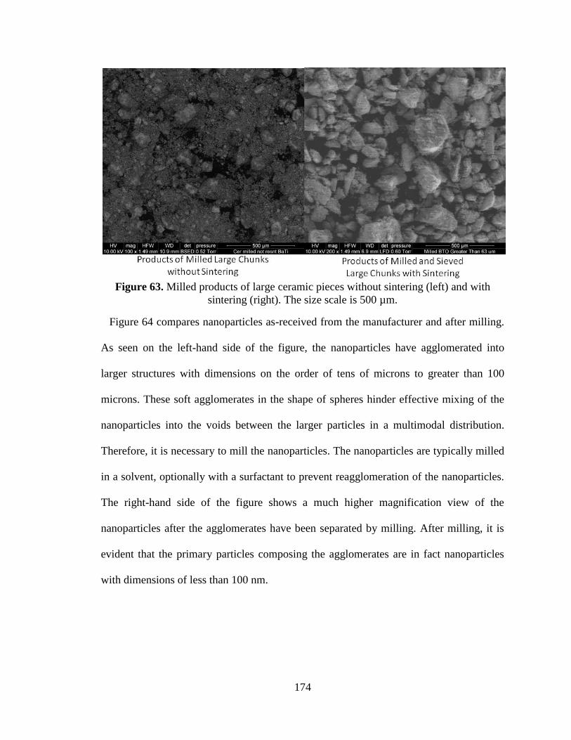
174
Figure 63. Milled products of large ceramic pieces without sintering (left) and with
sintering (right). The size scale is 500 µm.
Figure 64 compares nanoparticles as-received from the manufacturer and after milling.
As seen on the left-hand side of the figure, the nanoparticles have agglomerated into
larger structures with dimensions on the order of tens of microns to greater than 100
microns. These soft agglomerates in the shape of spheres hinder effective mixing of the
nanoparticles into the voids between the larger particles in a multimodal distribution.
Therefore, it is necessary to mill the nanoparticles. The nanoparticles are typically milled
in a solvent, optionally with a surfactant to prevent reagglomeration of the nanoparticles.
The right-hand side of the figure shows a much higher magnification view of the
nanoparticles after the agglomerates have been separated by milling. After milling, it is
evident that the primary particles composing the agglomerates are in fact nanoparticles
with dimensions of less than 100 nm.

175
Figure 64. Nanoparticles as received (left) and after milling (right). The size scale on the
left is 300 µm, and the size scale on the right is 500 nm.
Figure 65 displays micrographs of the intermediate size particles at 5,000 and 50,000
times magnification. The size of these particles is rated to be less than 3 µm. As both
sides of the figure show, the particles are within the specification without further
treatment, so the particles were used in the composites as received. In the right-hand side
of the figure, the particles seem to be formed as a dense formation of smaller primary
particles. Since the particles do not appear to be porous, the density of the particles is
believed to be adequate. The irregular shape of the particles may increase the particle
packing density as in the case of the large particles.

176
Figure 65. Intermediate size particles as received. The size scale on the left is 10 µm, and
the size scale on the right is 1 µm.
Figure 66 shows the cross-section of two composites containing a trimodal distribution
of particles. These cross-sections were obtained by fracturing the composites, and the
surfaces were imaged without polishing, allowing the topography of the fractured surface
to be seen. The composite on the left-hand side included large particles that were sized at
the high end of particle sizes used in the composites, including particles with dimensions
greater than 100 µm. Both cross-sections display the high degree of ceramic particle
packing and distribution of particle sizes.
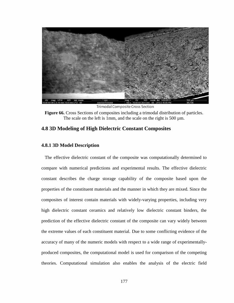
177
Figure 66. Cross Sections of composites including a trimodal distribution of particles.
The scale on the left is 1mm, and the scale on the right is 500 µm.
4.8 3D Modeling of High Dielectric Constant Composites
4.8.1 3D Model Description
The effective dielectric constant of the composite was computationally determined to
compare with numerical predictions and experimental results. The effective dielectric
constant describes the charge storage capability of the composite based upon the
properties of the constituent materials and the manner in which they are mixed. Since the
composites of interest contain materials with widely-varying properties, including very
high dielectric constant ceramics and relatively low dielectric constant binders, the
prediction of the effective dielectric constant of the composite can vary widely between
the extreme values of each constituent material. Due to some conflicting evidence of the
accuracy of many of the numeric models with respect to a wide range of experimentally-
produced composites, the computational model is used for comparison of the competing
theories. Computational simulation also enables the analysis of the electric field

178
distribution between the components comprising the composite. Another result of the
widely varying dielectric properties of the composite’s constituents is an unequal
distribution of the electric field. An understanding of how the electric field is distributed
is crucial for prediction of potential failure points due to electrical breakdown. Due to the
random nature with which many of the components are arranged in the composite, a
detailed analysis of the electric field distribution is effectively impossible without the aid
of computer analysis.
The model builds upon the advancements recently made in three-dimensional dielectric
composite modeling by other researchers [9, 10]. The model under consideration offers
some unique capabilities, including flexibility in the properties of the composite’s
components, as described in subsequent sections. The program’s operation is described,
and examples are given of an analysis on the difference between simulated and calculated
effective dielectric constant values and the visualization of the electric field distribution.
The modeling program was implemented as a macro in CST EM Studio. The macro
provides a user interface to input simulation parameters, check for errors, and automate
the process of creating the composite form, filling the composite with ceramic, polymer,
and voids, executing the electrostatic simulation, and calculating the parameters of
interest from the results of the simulation. This section will describe the flexibility built
into the macro in defining the composite parameters.
One of the significant differences between the simulation program being described and
similar previously-developed programs is the range of parameters that can be defined.
The program is built to accommodate up to six different materials in the composite. The
form of the composite is first filled with a solid matrix, which is usually defined with the

179
properties of a polymer that acts as the composite’s binder. Up to four additional
materials can be added as fillers, with the default use consisting of between 1 and 3
ceramic fillers and one material defined as voids. The morphology of the particles can be
any of the predefined shapes available in CST EM Studio, but cubes and spheres are
given as the only default options as they are the most common shapes encountered in real
particles.
Figure 67 shows a screen shot of the user interface developed for the program. The
input parameters occupy the left side of the interface, and the output from both the
particle-filling and electrostatic-modeling functions appears on the right side. For each of
the composite materials, the dielectric constant and mass density is entered into the
program. For the fillers and voids, the dimensions of the particles to be inserted into the
program are also included. The volume percentage of the total composite volume is user-
defined for the filler and voids. The user can then define the percentage of each filler
towards the total filler volume. Options also allow the composite to be built without
fillers and/or voids. The combination of all the parameters allows a substantial amount of
flexibility in the range of composites that the program can model.
When filling the composite with filler particles or voids, coordinates are randomly
generated, and the volume surrounding the coordinates is checked for other materials,
depending on the mode of insertion. Two modes of filler insertion are available based on
hard or soft modeling [9, 11]. Hard modeling does not allow two filler particles to
intersect. However, soft modeling does allow intersection, forming more complex filler
shapes as a new combined particle is effectively formed due to the intersection. Both
modeling methods have advantages under certain circumstances. However, in this

180
program, it has been determined that it is most practical to use hard modeling for
generating fillers and soft modeling for generating voids. This practice is intuitive as
individual ceramic particles will not be capable of merging without sintering, which is
not an option for the composites under development. Voids, often consisting of trapped
air, however, will effectively merge if placed adjacent to each other, so soft modeling is
appropriate for voids.
There are currently two potential sources for error in calculations of the effective
dielectric constant. The first source of error is the inclusion of the fringe capacitance in
the value returned by EM Studio in the capacitance matrix. The electrode and composite
diameters are equal, so the capacitance value returned by the program will include fringe
capacitance due to the surrounding volume occupied by a material with a dielectric
constant of 1. Since the fringe capacitance is dependent on the geometry of the
composite, it is difficult to precisely account for it. However, the error introduced by the
fringe capacitance is lower for a composite with a higher value of effective dielectric
constant. Inclusion of a method to account for the fringe capacitance is a potential future
improvement to the program. The second source of error is introduced when the edges of
neighboring filler particles or filler and void particles overlap. Although the program is
designed to model filler-filler and filler-void interactions with a hard model without
intersections, a small amount of edge intersections do occasionally occur. When a
location is randomly selected for placement of a particle, only a finite number of points
on that particle’s surface can be analyzed for conflict with other particles already in
place. Checking for conflicts at the defined locations along the surface of the new particle
prevents placement of particles with a significant overlap but does not always detect

181
overlapping edges. Although the intersecting volume is relatively small, the exact
percentage of overlap is indeterminable. This overlap introduces error during electrostatic
simulation as the program can only use the dielectric constant of one of the materials in
the overlapping region. Future improvements to the program can be made to either check
for conflicts at more surface points before particle placement and/or determine the
volume of intersecting edges.
Figure 67. Screen shot of the user interface displaying the control parameters for
composite construction
Figure 68 and Figure 69 show examples of composites generated by the macro. The
matrix was generated as a cylinder with a relatively low dielectric constant. Perfect
electrical conductors, which can be seen as semi-transparent plates in Figure 69, were
automatically generated on both sides of the composite to facilitate electrostatic
simulation. Spherical fillers were randomly generated and inserted into the matrix volume
of Figure 68, and Figure 69 shows a composite filled with cubic particles. Since the
simulations are meant to model real composites, partial particles at the edges of the
composite are not permitted. Once the composite has been generated through the

182
automated process according to the user’s specifications, an electrostatic analysis can be
performed, giving results for the capacitance, effective dielectric constant, and electric
field distribution.
Figure 68. Virtual composite filled with 4 types of spherical particles
Figure 69. Virtual composite filled with 2 types of cubic particles
A typical composite for a simulation is a cylinder 5 µm thick and 10 µm in diameter.
While these dimensions are small in comparison to the large composites produced in this
work, the dimensions must be kept on this scale to limit the number of mesh cells
generated during the simulation to a practical level of several million. Despite the
discrepancy between the sizes of the simulated volume and the physical composites, the
concept of simulating a small volume to predict the properties of a larger composite is
sound due to the homogeneity of the composites. The simulated dimensions effectively

183
correspond to simulating a small volume of a much larger composite consisting of many
equivalent volumes on the scale of that which is simulated. Two aspects of the
composites that cannot be directly replicated in the simulations are the size of the
particles and the ratio of the particle sizes. These constraints are also due to the practical
limits of the number of mesh cells. If 50 nm particles were to be simulated alongside 1
µm particles, the mesh size would have to be so small to adequately simulate the 50 nm
particles that the total mesh count would be unmanageable for a desktop system to
simulate. Therefore, the particle sizes are generally kept within a size range between 0.5
and 2 µm. The upper limit ensures that any one particle is less than half the thickness of a
5 µm thick virtual composite. The lower limit of 0.5 µm allows a distribution of particle
sizes to be used while keeping the mesh count to a realistic level. A drawback of the
limitation in the range of particle sizes is that very high levels of particle loading,
typically greater than 70%, are very difficult if not impossible to produce.
4.8.2 Model Results
Three-dimensional models of each of the composite classes were generated and
simulated in CST Microwave Studio using the volumetric content calculated from the
thermogravimetric analysis data in section 4.7. The composites were simulated as a
cylinder with a thickness of 5 µm and a diameter of 10 µm. Two particle sizes, typically
1.5 µm and 0.5 µm, were used to achieve a high volume percentage of filler particles.
Figure 70 shows the particles generated by the macro for simulation of MU100. The
electrodes and matrix material have been hidden in the figure to allow the particles to be
seen more clearly. In this example, the macro generated 1,369 total particles distributed
as 110 particles with a diameter of 1.5 µm and 1,259 small particles with a diameter of

184
0.5 µm. Both particle sizes represented ceramic fillers, and the total volume percentage
filled by the particles was approximately 66.8%.
Figure 70. Particles generated by the macro for the simulation of MU100
Table 17 lists the dielectric constant values used in the simulations for the ceramic,
binder, and voids in each of the composites. While the dielectric constant of barium
titanate can vary depending on the conditions, measurement method, and source of
information, a value of 100 was used in these simulations. The dielectric constant of the
CR-S in MU45 was estimated to be 5, reflecting the lower value of this polar binder at
high frequency. The dielectric constant of the PSSQ was assumed to be 2, which is
consistent with measurements of similar low density polysilsesquioxanes. For MU550, it
is assumed that the liquid filler is saturated throughout the volume of the binder, so a
value of 77 for EC50 was used for both binder and void values.
Table 17. Summary of dielectric constant values for the ceramic, binder, and voids used
in the three composite simulations
Ceramic εr Binder εr Void εr
MU45 1000 5 1
MU100 1000 2 1
MU550 1000 77 77
Table 18 lists the target volume percentages of each component. The volume percentages
of ceramic are the values calculated from thermogravimetric analysis. For MU45 and
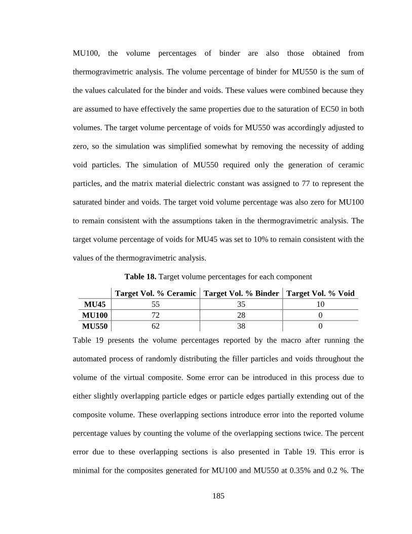
185
MU100, the volume percentages of binder are also those obtained from
thermogravimetric analysis. The volume percentage of binder for MU550 is the sum of
the values calculated for the binder and voids. These values were combined because they
are assumed to have effectively the same properties due to the saturation of EC50 in both
volumes. The target volume percentage of voids for MU550 was accordingly adjusted to
zero, so the simulation was simplified somewhat by removing the necessity of adding
void particles. The simulation of MU550 required only the generation of ceramic
particles, and the matrix material dielectric constant was assigned to 77 to represent the
saturated binder and voids. The target void volume percentage was also zero for MU100
to remain consistent with the assumptions taken in the thermogravimetric analysis. The
target volume percentage of voids for MU45 was set to 10% to remain consistent with the
values of the thermogravimetric analysis.
Table 18. Target volume percentages for each component
Target Vol. % Ceramic Target Vol. % Binder Target Vol. % Void
MU45 55 35 10
MU100 72 28 0
MU550 62 38 0
Table 19 presents the volume percentages reported by the macro after running the
automated process of randomly distributing the filler particles and voids throughout the
volume of the virtual composite. Some error can be introduced in this process due to
either slightly overlapping particle edges or particle edges partially extending out of the
composite volume. These overlapping sections introduce error into the reported volume
percentage values by counting the volume of the overlapping sections twice. The percent
error due to these overlapping sections is also presented in Table 19. This error is
minimal for the composites generated for MU100 and MU550 at 0.35% and 0.2 %. The

186
error is somewhat larger at 3.9% for MU45 due to the additional components added in the
form of voids. It should be noted that the volume percentage of ceramic achieved for
MU100 was approximately 66.83% or slightly more than 5% lower than the target
volume percentage. This discrepancy between the target and achievable value is due to
limitations in particle packing density achievable within the constraints of the simulated
volume and the practical ratio of particle sizes.
Table 19. The volume percentages of each component reported by the program after
automatic generation of the fillers and voids
Reported Vol.
% Ceramic
Reported Vol.
% Binder
Reported
Vol. % Void
Percent Error in Vol. %
Due to Overlap
MU45 52.92 41.73 8.88 3.53
MU100 66.54 33.82 0 0.36
MU550 59.37 40.83 0 0.2
Table 20 lists the simulated dielectric constants obtained from the 3D model along with
values calculated using Lichtenecker’s equation and the values of Table 17 and Table 19.
The percentage difference between the two dielectric constant values is also provided to
compare these two modeling techniques. MU550 was the simplest virtual composite due
to the common dielectric constant of the matrix material and void regions and the
relatively low volume percentage of fillers, both ceramic and voids, required. The
agreement between the Lichtenecker model and the simulated value is excellent for
MU550 with a percent difference of 3.34%. As the virtual composites become more
complex with higher filler loadings, additional error is introduced. The percent difference
between the mathematical model and the simulation for MU45 was just under 7%. The
percent difference for MU100 reached nearly 17%. This discrepancy is believed to be due
to the error introduced by very high filler loadings. As the filler loading reaches the
maximum values possible, there is increased overlap of the particle edges. The overlap of

187
the particle edges would constitute a violation of the assumption of a homogenous
mixture of individual particles assumed in the derivation of the Lichtenecker rule by
Simpkin [12]. The overlapping particles form a larger percolated mass similar to what
might be physically realized through sintering of the particles. Therefore, it is
unsurprising that the higher filler loading results in a greater percentage difference as the
simulation overestimates the dielectric constant.
Table 20. The dielectric constant obtained from the simulation, the dielectric constant
calculated from Lichtenecker's equation, and the percentage difference
Lichtenecker
Predicted εr From
Reported Vol. %
Simulated εr % Diff. Between Reported
Lichtenecker and Simulated Values
MU45 75.73 70.58 6.80
MU100 125.32 146.14 -16.62
MU550 355.92 367.8 -3.34
The 3D simulations of the effective dielectric constant of composites are most useful
for evaluating mathematical models of composites, but some comments can be made on
the agreement between the simulated dielectric constant and the measured values. The
dielectric constant value for CR-S used in the Lichtenecker model and simulation was 5,
corresponding to the high frequency value. The calculated and simulated composite
dielectric constants for MU45 of around 70-75 are about 36% higher than the typically
measured 45. The discrepancy could be a result of multiple causes. First, due to the
imperfect composite-probe contact, it is expected that the high frequency measurement is
an underestimation of the actual dielectric constant. Second, the value of 1000 assumed
for the dielectric constant of barium titanate may be slightly higher than its actual value
in the ceramics used in the composites. If a value of 21 were used as the dielectric
constant of CR-S for low frequency applicability, the Lichtenecker equation predicts a
dielectric constant of nearly 138. This value is reasonable in consideration of the low

188
frequency measurements of MU45 in which the dielectric constant was greater than 100
even under low electric field conditions.
Analysis of the calculated, simulated, and measured values of MU100 is very similar to
the case of MU45. The calculated and simulated values for MU100 are 19% and 39%
higher than the 200 MHz measured value of 105, respectively. The difference again could
be due to the imperfect composite-probe contact and the potentially high dielectric
constant value used for barium titanate. The theoretical values agree very well with the
low frequency measurement of MU100 under low electric field conditions, which was
previously reported to be 135.4 in Figure 43.
The discrepancy between the theoretical values of Table 20 and the high frequency
measurement of 550 is different than the cases of MU45 and MU100 as the theoretical
values are lower than the measured value. This difference is believed to be due to the
variation in the volume percentage of ceramic between different samples of MU550. Of
the three composites, MU550 exhibited the largest variation in properties from sample to
sample. This variance can be caused by several manufacturing issues. The first potential
cause is that the agar was allowed to cool and gel prior to the compaction of the
composite. With the gel formed, the density of the ceramic particles will be kept below
its potential maximum. Second, the solution of agar may have been prepared at too high
of a concentration, which also can cause the packing density to be limited. Third, not all
of the excess solution may have been pressed out of the slurry during compaction. This is
related to the first potential problem but could be due to other issues than premature
cooling. It is believed that when MU550 is prepared and pressed to its optimal density,
the ceramic density can be as high as a trimodal distribution of particles packed without a

189
binder. Indeed, if the Lichtenecker equation is evaluated with 77% ceramic and the
remaining volume occupied by polymer and voids saturated in EC50, the calculated
dielectric constant is approximately 554.5. This value can be measured more accurately
with the high frequency probe than MU45 or MU100 because excess EC50 on the surface
of the composite fills any voids along the composite-probe junction, limiting the effects
of air voids due to the imperfect contact.
190
References for Chapter 4
[1] "Agilent 85070E Dielectric Probe Kit Technical Overview," Agilent
Technologies 2008.
[2] "Agilent Technologies Impedance Measurement Handbook," Agilent
Technologies 2006.
[3] C. K. Chiang and R. Popielarz, "Polymer composites with high dielectric
constant," Ferroelectrics, vol. 275, pp. 1-9, 2002.
[4] C. B. Sawyer and C. H. Tower, "Rochelle salt as a dielectric," Physical Review,
vol. 35, pp. 269-275, 1930.
[5] "PA-80 and PA-100 Trigger Generators," L-3 Communications Pulse Sciences,
San Leandro, CA.
[6] W. Weibull, "A statistical distribution function of wide applicability," Journal of
Applied Mechanics, vol. 18, pp. 293-297, 1951.
[7] A. W. Coats and J. P. Redfern, "Thermogravimetric Analysis: A Review,"
Analyst, vol. 88, pp. 906-924, 1963.
[8] K. Nishinari, K. Kohyama, P. A. Williams, G. O. Phillips, W. Burchard, and K.
Ogino, "Solution properties of pullulan," Macromolecules, vol. 24, pp. 5590-
5593, 1991.
[9] K. Zhou and S. Boggs, "Effective dielectric constant of a linear matrix filled with
linear and nonlinear spherical particles," in 17th IEEE Inter. Pulsed Power Conf.,
Washington, D.C., 2009, pp. 342-345.
[10] P. Kim, N. M. Doss, J. P. Tillotson, P. J. Hotchkiss, M. J. Pan, S. R. Marder, J. Li,
J. P. Calame, and J. W. Perry, "High energy density nanocomposites based on
surface-modified barium titanate and a ferroelectric polymer," ACS Nano, vol. 3,
pp. 2581-2592, 2009.
[11] D. P. Bentz, E. J. Garboczi, and K. A. Snyder, "A hard core/soft shell
microstructural model for studying percolation and transport in three-dimensional
composite media," NIST, Gaithersburg, MD 1999.
[12] R. Simpkin, "A derivation of Lichtenecker's logarithmic mixture formula from
Maxwell's equations," IEEE Transactions on Microwave Theory and Techniques,
vol. 58, pp. 545-550, 2010.

191
Chapter 5: High Power Dielectric Resonator Antenna
5.1 Background on Dielectric Resonator Antennas
Dielectric resonators were first investigated in the late 1930s and were developed to
form compact circuit filters and oscillators [1]. The large difference in the material
properties of a high dielectric constant material and the surrounding medium create
boundary conditions at the walls of the resonator. These boundary conditions enable
standing wave patterns to form within the high dielectric constant material similar to
those formed due to the boundary conditions of a metal cavity waveguide [2, 3]. In this
way, high dielectric constant materials can form resonators similar to metal cavity
waveguides. When applied in filters and oscillators, dielectric resonators are often
metalized to prevent electromagnetic radiation from leaking from the circuit. However,
the radiating nature of the resonators can be exploited to make compact high frequency
antenna elements in the form of dielectric resonator antennas (DRAs). In this study,
DRAs are generally limited to cylindrical geometries in which a high dielectric constant
material with a dielectric constant of εr, radius of a [m], and height of h [m] acts as a
radiating resonator when excited by being placed on or near a driving circuit.
This work on the development of a dielectric resonator antenna for high power
applications in the VHF and UHF bands expands upon the state of the art of dielectric
resonator antennas in three significant ways. First, although DRAs have been shown to
operate over a large range of frequencies from 1.3 GHz to over 40 GHz, they are less
commonly implemented below 1 GHz [3]. Second, the peak power level for DRA design
of 1 GW is greater than all known power levels previously used to drive DRAs. The

192
uniqueness of the gigawatt-level power requirement undertaken in this effort extends the
power level orders of magnitude over the levels used in conventional applications. Third,
constructing the resonator of the DRA from high dielectric constant composite materials
significantly enhances the ability to form the resonator into larger and more complex
shapes.
Despite the differences in the frequency and power requirements from what have been
previously demonstrated with DRAs, the DRA has multiple factors that make it an ideal
choice for a compact, high power, dielectric-loaded antenna. First, the relationship
between the dielectric constant of the material forming the resonator and the resonator’s
dimensions enables the high dielectric constant of the composite materials to directly
reduce the size of the antenna with few additional factors influencing the antenna
dimensions. The size and weight of the DRA are the primary limiting factors on the
minimum operating frequency [3]. Since DRAs have traditionally been made with
sintered ceramics or glass-like materials, the size, availability, and manufacturability of
the resonators have been limited. By using the newly-developed high dielectric constant
composites, the DRAs can more easily be built in the larger sizes required for low
frequency operation. Even though the dimensions required for low frequency operation
are considered large for DRAs, the dimensions will remain several times smaller than
conventional low frequency antennas. Second, due to the flexibility in methods with
which the DRA modes can be excited, it is possible to drive the DRA without direct
connection between the high voltage metallic feed and the high dielectric constant
material. Microstrip, aperture, and even probe coupling techniques can be employed
without the conductor making direct contact with the high dielectric constant material.

193
Since the field enhancements at triple points formed at the edges of interfaces between
conductors and high dielectric constant materials can be extremely large, indirect
coupling is crucially important to integrating a high dielectric constant material into a
very high power system. Large field enhancements can significantly contribute to
premature dielectric breakdown in high voltage systems and must be avoided whenever
possible. The transmission line feeding the DRA can also be tailored to the high power
antenna requirements by utilizing large thicknesses of conventional insulators and
adjusting the other transmission line parameters to maintain the desired impedance. For
example, for a microstrip feed, the substrate thickness can be increased to withstand the
peak high voltage levels while the width of the transmission line can be increased to
maintain the characteristic impedance of the line. Thus, the DRA can be driven at very
high peak power levels without stressing the dielectrics of the substrate and without
making direct electrical contact with the high dielectric constant material. These unique
aspects of DRA feeding mechanisms make DRAs an attractive choice for compact high
power antennas.
5.2 Coupling Methods
Several options exist for coupling energy to the dielectric resonator, and the coupling
method employed can affect the resonant frequency and bandwidth of the antenna. Some
of the most common methods for coupling to a DRA include probe coupling, microstrip
coupling, aperture coupling, coplanar coupling, and dielectric image guide coupling [3].
Probe coupling involves inserting the end of a microstip or coaxial probe into or directly
onto the surface of the resonator. Since this metal-resonator connection will result in very
high field enhancements due to the triple points along the edge of the interface, probe

194
coupling is not considered a viable option for high power coupling. Coplanar coupling is
also excluded due to the potential for flashover between the coplanar strips driving the
resonator when driven at very high peak voltage. Lastly, dielectric image guide coupling
is generally beneficial to reduce conduction losses that would otherwise occur with
microstrip feeds at very high frequencies. Since the antenna will be designed for
relatively low frequencies, conduction losses are less of a concern, so dielectric image
guide coupling is not well suited for the present application. Microstrip and aperture
coupling offer effective means for coupling to the DRA, and both are considered further
as the coupling method of choice.
Microstrip transmission lines have been shown to be effective feeds for coupling to
DRAs [4]. Microstrip coupling can be achieved through either direct or proximity
coupling [3]. In direct coupling, the resonator is placed directly on the end of the
microstrip line. Since the direct connection between the microstrip and resonator will also
result in high field enhancements, direct coupling is not the preferred embodiment of
microstrip coupling. Proximity coupling drives a resonator that is removed from the
microstrip by a set distance. To improve the coupling, the resonator should be positioned
such that the fields created by the microstrip are incident in the resonator in regions of
high fields in the desired resonance mode. Figure 71 shows an example of proximity
microstrip coupling. The microstrip is formed by a conductor with a width, wm [m], over
a substrate with a defined dielectric constant, εsub, and thickness, tsub [m]. The distance
between the microstrip and the resonator, s [m], can be altered to maximize the coupling.
The resonator is separated from the microstrip conductor by a small gap distance, which
is not labeled due to the small scale, to prevent direct metal-composite contact.

195
Figure 71. Microstrip coupling
Aperture coupling is similar to microstrip coupling. However, unlike microstrip
coupling, the resonator is on the opposite side of the substrate from the transmission line.
The antenna can be driven with a microstrip similar to proximity microstrip coupling, or
a coaxial cable or other transmission line can be implemented. A microstrip was
primarily considered for its advantages in custom fabrication. To couple energy between
the microstrip and resonator, an aperture is cut into the ground plane, and the resonator is
placed on or near the aperture. Figure 72 shows the critical parameters for designing an
aperture-coupled DRA driven by a microstrip. The resonator has been removed from the
figure to reveal the aperture and critical dimensions, but the resonator would normally be
placed over the aperture to couple to the fields passing through the ground plane. A
microstrip, shown on the opposite side of the substrate with dashed lines, again has a
width of wm [m]. The substrate has a thickness of tsub [m] and a dielectric constant of εsub.
The rectangular aperture is shown as a slot in the ground plane with a width, ws [m], and
length, ls [m]. The slot length must be large enough to effectively couple to the resonator

196
but not so large that a significant back lobe is radiated on the microstrip side of the
substrate [3].
Figure 72. Aperture coupling with resonator removed
Equation (5.1) is recommended as a starting value for the slot length [3].
(5.1)
The symbol εe in equation (5.1) is a dielectric constant value calculated as the average of
the resonator and substrate dielectric constants. The slot width is also constrained to limit
the formation of a back lobe, and a width equal to 20% of the slot length is typical [3].
The microstrip is often extended beyond the aperture by a stub length, s [m], to cancel out
the admittance of the aperture and improve the impedance match to the resonator [3]. A
recommended initial stub length is a quarter of the guided wavelength of the wave in the
substrate, and the stub length can be adjusted to improve impedance matching [3].
One of the advantages to microstrip and aperture coupling is the ability to mechanically
tune the antenna to maximize coupling by moving the resonator with respect to the
microstrip or aperture without requiring significant alterations to the fixed pieces of the
antenna. Additionally, the substrate thickness can be increased as needed to hold off the
high voltage signal driving the antenna, and the microstrip width can be increased to

197
maintain the desired line impedance as the substrate thickness is increased. Both
microstrip and aperture coupling have the potential to drive a high permittivity, low
profile resonator. However, due to the potentially thick substrates required to hold off the
peak voltage at high power, the coupling factor obtained through aperture coupling may
be degraded. Therefore, microstrip coupling was chosen as the preferred coupling
method.
5.3 Resonant Modes a Cylindrical Dielectric Resonator
Due to the relatively developed state of the design parameters for cylindrical resonators
and the convenience of implementing resonators with the same shape formed with
cylindrical dry pressing dies, cylindrical dielectric resonator antennas were the primary
antenna geometry under consideration. The cylindrical DRA offers a degree of freedom
to the designer in which the ratio of the cylinder radius, a [m], to the cylinder height, h
[m], can be adjusted to change the resonant frequency [3]. Two values of the ratio will
correspond to the same operating frequency but with different Q-factors [3]. Thus, either
a relatively short and wide cylinder or a relatively long and thin cylinder can be designed
for the same operating frequency depending on constraints due to the Q-factor or form
factor of the antenna.
Examination of the lower-order modes of a cylindrical DRA is necessary to determine
the resonant frequency, Q-factor, and radiation patterns available for resonators in a range
of practical dimensions. The most common radiating modes of the cylindrical DRA, as
reported by Petosa, are the TM01δ mode, the TE01δ mode, and the HE11δ mode [3]. The TE
and TM designations correspond to transverse electric and transverse magnetic modes,
respectively, and the HE1δ mode is a hybrid mode in which the Ez component is dominant
198
over the Hz component [3]. The mode subscripts correspond to field variations in the
directions of the cylindrical coordinates of the azimuth, radius, and center axis,
respectively. The symbol δ takes a value between zero and one with a higher value
corresponding to a higher dielectric constant material comprising the resonator [3]. The
equivalent radiating sources of the TM01δ, TE01δ, and HE11δ modes are a short electric
monopole, short magnetic monopole, and a short horizontal magnetic dipole, respectively
[3].
The fundamental mode for cylindrical radiators has been cited by some sources to be
the TM110 mode [5, 6]. The original work on dielectric resonator antennas by Long et al.
derives the frequency of the fundamental mode of a cylindrical cavity as equation (5.2)
[5, 6]. The symbol X11 represents the first zero of the Bessel equation describing the
fields inside the resonator and is equal to 1.841.
(5.2)
It is easily shown that when the condition of equation (5.3) is met, the resonant
frequency’s dependence on the radius is diminished and equation (5.2) is reduced to
equation (5.4).
(5.3)
(5.4)
Equation (5.4) has been shown to be applicable for other low profile antenna shapes,
including rectangles and triangles, in which the width dimensions of the antenna are
much larger than the thickness [3, 7]. The lack of dependence on the radius or other width

199
dimension is due to the resonance arising from waves reflections between the top and
bottom of the resonator [6].
Plots have been prepared showing the fundamental frequency for radii of 1.27, 3.81,
and 5.72 cm. These radii correspond to dry pressing dies that were in use during the
course of this work. Figure 73 shows the plot of equation (5.2) for the cylindrical DRA
excited in the TM110 mode with a resonator dielectric constant of 100. It is clear that for
small values of h, which correspond to large values of a/h, the radius of the resonators is
negligible. The resonant frequencies of the resonators with all three radii are essentially
indistinguishable up to a thickness of at least 5 mm. The frequency of the resonator with
the smallest radius quickly loses its independence from the radius as it fails to meet the
condition of equation (5.3) as the thickness increases. Although the difference between
the frequencies of the resonators with radii of 3.81 cm and 5.72 cm gradually increases,
the difference is relatively small due to the weak dependence on the radius when a/h
remains large. Both resonators with a large radius have resonant frequencies below 300
MHz at thicknesses below 5 cm. The resonant frequency of the resonator with a radius of
5.72 cm reaches below 200 MHz at a thickness above 5 cm.

200
Figure 73. Resonant frequency of cylindrical DRA with εr = 100 in TM110 mode
Equation (5.2) was also applied for resonators incorporating the MU550 composite as
shown in Figure 74. The very high dielectric constant value of 550 results in a frequency
reduction to below 200 MHz in resonators with radii of 3.81 cm and 5.72 cm. Even the
resonator with a radius of just 1.27 cm extends below 500 MHz with a thickness of just 1
cm. Since equations were unavailable to calculate the quality factor of the TM110 mode, it
cannot be directly compared to the other resonant modes in this analysis. However, due to
the very low frequencies predicted in Figure 73 and Figure 74 and the proven
effectiveness of low-profile antennas incorporating high permittivity materials at higher
frequencies with this mode, it is a preferred mode for excitation.

201
Figure 74. Resonant frequency of a cylindrical DRA with εr = 550 in TM110 mode
Equation (5.5) describes the relationship between the resonator dimensions and the
fundamental wave number, k0 [m-1
], of the TM01δ mode [3].
(5.5)
The fundamental wave number is related to the fundamental wavelength, λ0 [m], and
frequency, f0 [Hz], according to equation (5.6), in which c [m/s] is the speed of light in
vacuum [8].
(5.6)
Equation (5.5) can be used to predict the center frequency of operation for a resonator
with chosen radius and height dimensions. The bandwidth is determined by the quality,
Q, factor, which is given as equation (5.7) for the TM01δ mode [3]. The dielectric constant

202
of the material comprising the resonator at the center frequency can be used as the value
for εr.
(5.7)
The quality factor is inversely proportional to the bandwidth, Δf, of the antenna as shown
in equation (5.8) [2]. Resonators made from very high dielectric constant materials often
have higher Q-factor values, so it is imperative to design the antenna to reduce the quality
factor to maintain an acceptable bandwidth while maintaining efficiency. Techniques to
reduce the quality factor and increase the bandwidth are covered later in this chapter.
(5.8)
Implementation of very high dielectric constant materials can further increase the Q-
factor to impractically high values, so whenever possible, it is advantageous to design for
a lower Q-factor.
Figure 75 shows the resonant frequency of the cylindrical DRA excited in the TM01δ
mode. Since the dielectric constant of 100 can be considered high, the mode is likely
close to that of the TM011. While the frequency of operation for a DRA with a radius of
1.27 cm remains relatively high with a minimum of approximately 1.5 GHz, the
frequency of the DRAs with radii of 3.81 cm and 5.72 cm reach below 500 MHz and 325
MHz, respectively, as the thickness in increased to a few centimeters. The low
frequencies of the DRAs with radii of 3.81 and 5.72 cm are within an acceptable range,
but the quality factor of these antennas may be impractically high, as shown in Figure 76.
Quality factor values of 1000 or greater would result in an impractically-small

203
bandwidth, which would make the antenna very difficult to drive without a very specific
high power source. Therefore, the Q-factor must be appropriately reduced for the TM011
mode to be effective in the operation of the DRA.
Figure 75. Resonant frequency for cylindrical DRA with εr = 100 in TM011 mode

204
Figure 76. Quality factor of cylindrical DRA with εr = 100 in TM011 mode
Equation (5.9) relates the fundamental wave number and resonator dimensions for the
HE11δ mode , and the equation for the HE11δ Q-factor is given as equation (5.10) [3].
(5.9)
(5.10)
A graph of the resonant frequency obtained by applying equation (5.9) for radii of 1.27,
3.81, and 5.72 cm is shown in Figure 77. The shape of the curves is similar to that seen
from the TM011 mode plot, but the frequencies reach even lower levels at thicknesses
larger than 1 cm. The frequency of the 3.81 cm radius resonator dips below 275 MHz at
large thicknesses, and the frequency of the 5.72 cm radius resonator extends below 200
MHz as it approaches a thickness of 10 cm. In addition to the lower frequencies
achievable in this mode, the quality factor is much lower. The quality factor for the three
resonator radii varies between 40 and 160. While these values are higher than desired, the
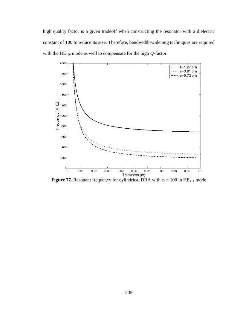
205
high quality factor is a given tradeoff when constructing the resonator with a dielectric
constant of 100 to reduce its size. Therefore, bandwidth-widening techniques are required
with the HE11δ mode as well to compensate for the high Q-factor.
Figure 77. Resonant frequency for cylindrical DRA with εr = 100 in HE111 mode

206
Figure 78. Quality factor for a cylindrical DRA with εr =100 in HE111 mode
Equations (5.11) and (5.12) show the relationships utilized to determine the resonant
frequency and quality factor of a cylindrical resonator excited in the TE01δ [3].
(5.11)
(5.12)
The graphs of the TE01δ mode resonant frequency and Q-factor produced with equations
(5.11) and (5.12) are shown as Figure 78 and Figure 79, respectively. At large
thicknesses, the frequencies of the three resonators are slightly greater than those
predicted in Figure 77 for the HE111 mode. The most interesting aspect of Figure 79 is
how, unlike the previously-considered modes, the resonant frequency decreases at very
small thicknesses. This effect is only seen in the resonators with radii of 3.81 and 5.72 cm

207
as the effect does not occur for the resonator with a 1.27 cm radius in the thickness range
considered above 1 mm. It remains to be determined through electromagnetic simulations
whether this effect is real or is the result of a breakdown in the equations, which were
developed for lower ratios of a/h. Although this behavior in the calculated resonant
frequencies for small thicknesses was not investigated further in this work, it is believed
that the equations are likely not valid for such small thicknesses and low frequencies with
very thin layers are not possible. The Q-factor of the TE01δ mode reaches a peak slightly
greater than that seen in the HE11δ mode. However, the Q-factor is less than 80 in the
range of relatively thin thicknesses for which the frequency is predicted to be very low.
Figure 79. Resonant frequency of a cylindrical DRA with εr = 100 in TE011 mode

208
Figure 80. Quality factor of a cylindrical DRA with εr = 100 in TE011 mode
5.4 Bandwidth Enhancement
As previously shown in equation (5.8), the quality factor and the bandwidth of the
resonator are inversely related. The utilization of high dielectric constant materials as the
resonator can result in a very high Q-factor, so methods have been developed by previous
researchers to actively increase the bandwidth. The unloaded Q-factor, Q0, can be defined
through its contributing factors of the conductor loss quality factor, Qc, dielectric loss
quality factor, Qd, and radiation loss quality factor, Qr, as shown in equation (5.13) [2].
(5.13)
The relationship of equation (5.13) causes the unloaded Q-factor to be limited by the
lowest contributing Q-factor. The conductor power loss should be low in the DRA, so Qc
should not be the limiting factor. The radiation loss Q-factor can limit the unloaded Q-
factor. The radiation loss Q-factor, given as equation (5.14), is low if the ratio of the peak

209
stored energy, W [J], to the radiated power, Pr [W], is low [2]. The symbol ω0 [rad/s] is
the resonant angular frequency.
(5.14)
When dominated by the radiating loss Q-factor, the bandwidth is usually only a few
percent. Therefore, the dielectric loss quality factor or other techniques must be utilized
to increase the bandwidth. Although the losses of the high dielectric constant composites
are generally kept as low as achievable to limit the amount of wasted energy, some losses
in the dielectric can improve the bandwidth significantly. The dielectric loss quality
factor, defined by equation (5.15), has an inverse relationship with the dielectric losses.
Therefore, a lossy material will result in a low value for Qc and a relatively low unloaded
quality factor [2].
(5.15)
The dielectric losses below 500 MHz are relatively low for all three composite materials.
The losses can be considered to be within the range of 0.01 and 0.15, which all of the
composites have been measured to remain under up to at least 500 MHz. Figure 81 shows
the plot of the dielectric loss quality factor and the corresponding bandwidth as functions
of the dielectric losses of the resonator.

210
Figure 81. Dependence of the dielectric loss quality factor and bandwidth with respect to
the dielectric losses of the resonator
As shown in Figure 81, the dielectric loss values of 0.01 and 0.1 correspond to Qd factors
of 100 and 10, respectively, and bandwidths of 1% and 10%, respectively. If the
dielectric losses at the resonant frequency are somewhere in the middle of this range at
around 0.05, the unloaded Q-factor will likely be dominated by the dielectric losses, and
the bandwidth will be approximately 5%. A bandwidth of 5% is sufficient for many
applications and is higher than achieved in many lower permittivity low loss resonators.
Other techniques may be necessary to further increase the bandwidth beyond that
predicted from the dielectric loss quality factor to adequately couple the signal from the
high power antenna driver. Several bandwidth-enhancement techniques for DRAs have
previously been investigated, but the current discussion is limited to multi-mode
excitation, multiple resonators, introduction of air gaps, and addition of microstrip stubs.
The excitation of multiple modes in the same resonator can broaden the bandwidth

211
without physically modifying the resonator or microstrip line. An examination of the
resonant frequencies of the modes analyzed earlier in this chapter shows that the resonant
frequency of some modes are close enough that exciting both modes could result in either
wideband or dual-band operation. For the excitation of more than one mode to truly be
considered wideband, it is often necessary that the radiation pattern of the two modes be
similar [3].
A second relatively straightforward approach to increasing the bandwidth is to include
multiple resonators along the same microstrip. If the resonators are made with different
dimensions or different materials, they can be designed to have slightly offset resonant
frequencies that combine to create an effective wideband antenna. The main disadvantage
to this approach is the increased size of the antenna through the addition of multiple
resonators. It is possible to minimize the overall size increase by either stacking the
resonators or even embedding the resonators within each other [3]. The stacked or
embedded resonators can still be individually excited at distinct resonant frequencies that
cause the antenna as a whole to operate with an increased bandwidth.
Elevating the resonator to add a gap between the resonator and conductor has also been
shown to greatly increase DRA bandwidth [3]. In one study, the bandwidth was increased
from 4.2% to 40% through the addition of a 10 mm air gap [3]. The use of a solid foam
can effectively add an air gap while providing mechanical support for the resonator since
the effective dielectric constant of an air-filled foam is approximately 1 [3].
The final method considered for increasing the bandwidth is adding a microstrip stub.
Since the preferred method of coupling has been selected to be microstrip coupling, the
addition of a stub to the end of the microstrip line is a simple modification that can

212
improve the impedance match of the circuit. Both L-shaped and T-shaped stubs have
been proven effective by other researchers [3]. By implementing one or more of the
bandwidth-widening techniques, the bandwidth can likely be increased above 10%
without significantly altering the resonator or feed circuit volume.
5.5 DRA Design
Dielectric resonator antennas were designed and built in this investigation for both low
power and high power evaluation. This description will be limited to a high power DRA.
To drive the antenna at power levels up to 1 GW with an antenna input impedance of
approximately 50 Ω, the applied voltage to the antenna must be nearly 225 kV. To
withstand these voltage levels, the high power antenna was designed for operation with a
very thick dielectric substrate. As shown in photos of the high power DRA of Figure 82
and Figure 83, the substrate was designed to be a 1.91 cm thick piece of polyethylene
measuring approximately 30.5 cm by 30.5 cm.
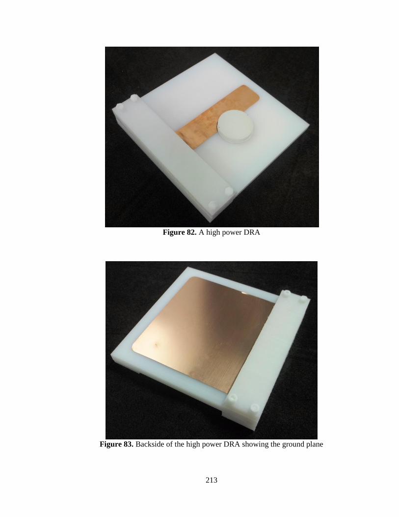
213
Figure 82. A high power DRA
Figure 83. Backside of the high power DRA showing the ground plane

214
While this large thickness enables operation at high voltage, it also requires an
exceptionally wide microstrip to match to the 50 Ω cables used for low power
characterization without employing additional matching techniques. The dimensions of
the microstrip were calculated using Wheeler’s formulas shown in equations (5.16) and
(5.17) [9]. The characteristic impedance of the microstrip, Z0 [Ω], is calculated in
equation (5.16) from this semi-empirical equation based on the dielectric constant of the
substrate, εsub, the thickness of the substrate, tsub [m], and the effective microstrip width,
w’m [m].
(5.16)
The effective microstrip width is slightly altered from the actual microstrip width, wm
[m], due to effects from the conductor thickness, tc [m], and the dielectric constant of the
substrate. The effective strip width can be calculated from equation (5.17) [9].
(5.17)
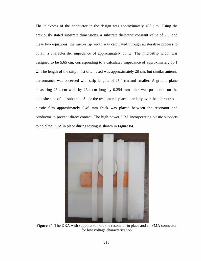
215
The thickness of the conductor in the design was approximately 406 µm. Using the
previously stated substrate dimensions, a substrate dielectric constant value of 2.5, and
these two equations, the microstrip width was calculated through an iterative process to
obtain a characteristic impedance of approximately 50 Ω. The microstrip width was
designed to be 5.65 cm, corresponding to a calculated impedance of approximately 50.1
Ω. The length of the strip most often used was approximately 28 cm, but similar antenna
performance was observed with strip lengths of 25.4 cm and smaller. A ground plane
measuring 25.4 cm wide by 25.4 cm long by 0.254 mm thick was positioned on the
opposite side of the substrate. Since the resonator is placed partially over the microstrip, a
plastic film approximately 0.46 mm thick was placed between the resonator and
conductor to prevent direct contact. The high power DRA incorporating plastic supports
to hold the DRA in place during testing is shown in Figure 84.
Figure 84. The DRA with supports to hold the resonator in place and an SMA connector
for low voltage characterization

216
The high dielectric constant composite material chosen as the resonator material in the
high power DRA was MU100 [10]. MU100 was selected for combining several desirable
properties, including a high dielectric constant of approximately 100 in the frequency
range of interest, relatively low dielectric losses, high dielectric strength, and robust
mechanical strength.
Based on the graphs of the resonant frequencies presented earlier in this chapter, the
radius of the resonator was designed to be 3.81 cm. The thickness of the resonator was
approximately 1.25 cm. From the equations in Section 5.3, the resonant frequency of a
dielectric resonator with fixed dimensions is a function of the permittivity of the
resonator. Since the permittivity of the composite is a function of frequency, calculation
of the resonant frequency of the resonator is a recursive process. Table 21 summarizes
the resonant frequencies calculated for the four modes considered earlier in this chapter
when accounting for the slight dependence of the dielectric constant of MU100 with
frequency. The lowest resonant frequency was calculated for the TE01 mode at 455 MHz.
The resonant frequencies of the TM110 and HE11 modes are only separated by 35 MHz at
650 MHz and 685 MHz, respectively. The highest frequency calculated for these four
modes was 770 MHz for the TM01 mode. While this analysis has concentrated on these
four modes due to reference to these modes in dielectric resonator antenna literature,
there are other modes that can potentially be excited within the frequency range covered
by these modes and above 770 MHz. It is possible to excite these four modes and others
with the same coupling method, so there is significant potential for multimodal operation
of the DRA as a bandwidth enhancement method.

217
Table 21. Resonant frequency calculated for the four modes considered in Section 5.3
Mode TM110 HE11 TE01 TM01
Resonant Frequency (MHz) 650 685 455 770
The high power DRA was intended to be operated in a bath of transformer oil. High
voltage breakdown issues are the primary motivation for the inclusion of transformer oil,
but there are additional benefits from incorporation of the oil. First, the dielectric
constants of the oil and the polyethylene components comprising the substrate and
resonator holders are very similar. The match of these dielectric constants results in the
environment around the resonator and microstip appearing to electrically be one material.
This continuity of the permittivity around the resonator and microstip minimizes the
effects of placing the plastic holders around the DRA to hold it in place. The electric field
is distributed around the resonator and conductors as if only a single low dielectric
constant material were present. Second, the oil flows into the small gap between the
microstrip conductors and the polyethylene substrate to limit the potential for impedance
variation along the transmission line due to the imperfections of the conductor-substrate
contact. By ensuring consistency of the transmission line impedance, reflections along
the line are reduced, and the return loss of the antenna is improved.
The placement of the DRA along the microstrip was determined experimentally by
observing the return loss as the resonator position was moved. This tuning process was
conducted in an oil bath. The ease with which the DRA can be tuned in this manner is a
significant advantage over more permanent antenna designs that require extensive
modification to tune the antenna for optimal performance.

218
5.6 DRA Evaluation Methods
5.6.1 Simulation of the Antenna Reflection Coefficient and Radiation Pattern
The dielectric resonator antenna was simulated using CST Microwave Studio. CST
Microwave Studio, like the CST EM Studio package chosen to model particle loading of
composites, enables the virtual construction and electromagnetic simulation of
components. CST Microwave Studio is specifically suited for performing transient and
frequency domain simulations of high frequency problems. The primary simulation
parameters of interest are the scattering, S, parameters and the far-field gain and radiation
pattern. The simulations were performed in the VHF and UHF bands from 20 MHz to 2
GHz.
The S11 parameter provides information on the impedance mismatch of the dielectric
resonator antenna and feed structure with an idealized port of known impedance. The S11
parameter is determined as the ratio of the reflected, V- [V], and incident, V
+ [V], voltage
magnitudes, as given in equation (5.18) [11].
(5.18)
The S11 parameter is the primary S-parameter of interest as it determines the input return
loss, RLin [dB], according to equation (5.19) [11].
(5.19)
As the impedance of the DRA is a function of frequency, the S11 parameter is also a
function of frequency. The S11 parameter and input return loss must be minimal at the
desired frequencies of operation. Low input return loss indicates matched impedance and
efficient energy transfer to the antenna.

219
In addition to the S-parameters, the far-field gain pattern of the DRA was simulated.
The gain, G, in equation (5.20) is an indicator of an antenna’s performance in comparison
to an antenna standard, which is often an isotropic radiator. The gain is reported in units
of dBi, GdBi [dBi], to indicate that the gain is with respect to an isotropic source [12].
(5.20)
The gain calculated from equation (5.20) is sometimes referred to as the realized gain
because the efficiency term eantenna includes both the radiation efficiency, erad, and the
mismatch loss due to the return loss. The radiation efficiency accounts for antenna losses,
which can include ohmic losses in the conductors or dielectric losses in the high dielectric
constant material. The radiation efficiency should be as high as possible, as all antenna
losses reduce the radiated power. The directivity, D, represents the ratio of the maximum
power density an antenna produces in a particular direction to the average power density
in all directions. The desired directivity is dependent on the antenna’s application. If the
antenna is intended to radiate with a small beam angle in only one direction, the
directivity must be high. However, antennas designed to radiate along the horizon in an
omnidirectional pattern will require a lower directivity and corresponding lower gain
value.
5.6.2 Low Voltage Measurements
Low power measurements were taken with an Agilent E5071C network analyzer in an
anechoic chamber. For consistency with the antenna’s intended use on high voltage
systems, the antenna’s performance was characterized with the DRA immersed in oil.
The return loss was measured directly with the network analyzer from 20 MHz to 4.5
GHz. The gain was measured in a single direction broadside to the substrate of the DRA

220
that was identified to be the center of the main lobe from simulations. The gain was
calculated from two-port scattering parameter measurements taken with a reference
antenna with a flat gain profile over the frequencies of measurement. The reference
antenna was selected to be a Sunol Sciences LP-80 log periodic antenna with a reported
typical gain of 6 dBi from 80 MHz to 2 GHz [13]. The log periodic antenna and the
interior of the anechoic chamber are shown in Figure 85.
Figure 85. The DRA was characterized at low power in the anechoic chamber with an
LP-80 log periodic antenna from Sunol Sciences.
Whereas the LP-80 is linearly polarized, the DRA should be considered elliptically
polarized for the purposes of gain measurements. Therefore, any single gain
measurement includes polarization mismatch. The polarization mismatch between the log
periodic antenna and the DRA were accounted for by taking two measurements with the
log periodic antenna maintained at vertical polarization and the DRA rotated 90° between
measurements. The ratio of the power received, Pr [W], to the power transmitted, Pt [W],
is calculated from the S21 [dB] scattering parameter measured by the network analyzer by
equation (5.21).

221
(5.21)
With the known gain of the LP-80 in linear scale, GLP80, the linear gain of the DRA to the
vertical polarization of the LP-80, GDRA,pol, can be calculated with equation (5.22) based
on the Friis transmission formula [8]. The frequency of the measurement and speed of
light are represented by f [Hz] and c [m/s], respectively, and the distance between the
antennas is represented by R [m].
(5.22)
These measurements are conducted twice with the DRA rotated by 90° between
measurements. The two linear gain values can be added to establish the total gain of the
DRA on a linear scale by equation (5.23) [14]. The gain of the DRA can then be
converted to decibels with equation (5.20).
(5.23)
The feed requirements of the low voltage and high voltage antenna measurements have
significant differences. Since the high frequencies measured with the network analyzer
can extend up to 4.5 GHz, 50 Ω coaxial cables with SMA connectors were used to
connect the network analyzer to the high power antenna. The thick substrate of the
microstrip on the high power DRA makes unmodified connection to an SMA connector
difficult, but poor coupling of the high frequency cable to the high power microstrip
could distort the measurements. A small tab extending from the ground plane and an
SMA adapter were added at the microstrip feed for the low power measurements to
facilitate connection between the microstrip, the ground plane of the DRA, and the SMA
connector of the coaxial cable. For consistency, the grounded tab is also included in the

222
model used for antenna simulations. The small ground tab and low voltage connectors
were removed for high power testing. The antenna feed for high power testing was
typically a stripline feed insulated in the oil bath. For optimal operation at full power, the
insulator of the stripline feed should be formed from an extension of the same piece of
material as the substrate of the antenna to reduce the risk of flashover at the antenna feed.
5.6.3 Comparison with Fundamental Limits for Electrically Small Antennas
Finally, based on the simulated and measured data obtained from the previous two
evaluation methods, the performance of the antenna is compared with the theoretical
fundamental limits established for electrically small antennas. Practical limits to the
minimization of the antenna size arise from degradation of antenna performance factors
including efficiency, gain, and bandwidth. The definition of an electrically small antenna
is inconsistent between various sources. A common rule-of-thumb definition of an
electrically small antenna is that the dimensions of the antenna are less than one-tenth of
the free space wavelength, λ [m] [15]. A more rigorous definition from Wheeler proposes
that an electrically small antenna has a radius that is a small fraction of the radiansphere
with a radius of λ/2π2 [16]. The near field region is predominantly inside the radiansphere
while the far field region is predominantly outside the radiansphere [16].The product of
the free-space wavenumber, k [m-1
], and the radius, R [m], of a sphere enclosing an
antenna is used as a metric for analysis of antenna size. The free-space wavenumber has
previously been defined in equation (5.6).
Wheeler’s definition for an electrically small antenna results in the condition that the
product of the free-space wavenumber and radius of the sphere circumscribing the
antenna be equal to or less than 1 [16]. However, a more strict definition arises from

223
Wheeler’s condition that the largest dimension of an electrically small antenna is less
than 1/k, providing the limit described by equation (5.24) [16].
(5.24)
Commonly referenced works by Chu and Harrington derived practical limitations on
antenna size [17, 18]. Both works consider theoretical antennas that fit within a sphere of
radius R [m]. The radiated fields outside the antenna can be described by the propagating
modes within the sphere [19]. When the size of the sphere is decreased to the point at
which one or zero modes can propagate within it, fundamental limitations are reached
[19]. While it is still possible for the antenna to operate within spheres smaller than these
limits, there are significant tradeoffs, including very high fields within the sphere, very
high Q and correspondingly low bandwidth, and/or poor efficiency due to impedance
mismatch [19].
Chu focused specifically on omnidirectional antennas, analyzing the increase in Q with
the decrease of the sphere size circumscribing the antenna [17]. Since the bandwidth can
be described as the inverse of Q, electrically small antennas can suffer from very low
bandwidth. When kR is much less than 1, Chu’s equation for Q is reduced to a
dependence on (kR)-3
[19]. Therefore, a practical limit is imposed on the minimization of
antennas, as evidenced through Chu’s analysis of omnidirectional antennas, in which the
bandwidth is reduced disproportionately with reduction in antenna size. When the
antenna is lossy, the Q is lowered, and the bandwidth is increased at the expense of
efficiency [19]. While the radiating field of the DRA considered in this work is not
omnidirectional, these concepts apply to the reduction in the antenna size with increasing
dielectric constant of the resonator. As the resonator dielectric constant is increased to

224
reduce the size of the resonator, the Q is increased. The increased Q will limit the
bandwidth, and design modifications are necessary to maintain an acceptable bandwidth.
Harrington’s work was also derived from analysis of antennas circumscribed by a
sphere, but this work is not specific to omnidirectional antennas [18]. A practical limit to
the gain achievable by an antenna circumscribed by a sphere with radius R was
established by Harrington by considering the point at which fields at the antenna structure
would become excessively large to have any practical radiated field [18]. The maximum
gain based on this practical limit is defined as the normal gain and given by equation
(5.25) [18].
(5.25)
While it is theoretically possible to achieve gains larger than that predicted by equation
(5.25), the fields at the antenna structure would be impractically large [18]. Gain beyond
the normal gain is described by the concepts of supergain or superdirectivity [18, 19].
5.7 DRA Simulation and Experimental Results
5.7.1 Simulation Results
The high power DRA was simulated with the transient solver of CST Microwave
Studio to predict the return loss, realized gain, and far-field pattern between 200 MHz
and 2 GHz. The measured permittivity of MU100 was directly imported into CST to
obtain a close numerical fit for simulation of the dielectric resonator’s properties. The
material around the antenna was defined to be oil for high power operation. Figure 86
shows the high power DRA as it was simulated. The red plane at the antenna feed is the
waveguide port used to feed the antenna.
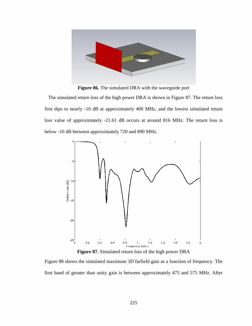
225
Figure 86. The simulated DRA with the waveguide port
The simulated return loss of the high power DRA is shown in Figure 87. The return loss
first dips to nearly -10 dB at approximately 400 MHz, and the lowest simulated return
loss value of approximately -21.61 dB occurs at around 816 MHz. The return loss is
below -10 dB between approximately 720 and 890 MHz.
Figure 87. Simulated return loss of the high power DRA
Figure 88 shows the simulated maximum 3D farfield gain as a function of frequency. The
first band of greater than unity gain is between approximately 475 and 575 MHz. After

226
briefly dipping to below unity gain, the gain remains positive above approximately 625
MHz.
Figure 88. Simulated maximum 3D farfield gain of the high power DRA
While Figure 88 plots the maximum 3D gain, the gain of greatest interest is that which is
orthogonal to the plane of the DRA substrate. In the polar coordinates shown in Figure
90, this direction corresponds to θ=φ=0°. Figure 89 plots the simulated gain orthogonal to
the substrate. The gain is briefly positive between approximately 475 and 525 MHz, and
the main band of high gain operation occurs between approximately 625 MHz and 1.05
GHz. The gain is above 5 dBi between approximately 670 and 920 MHz, and the peak
gain at θ=φ=0° is simulated to be nearly 7.5 dBi at approximately 829 MHz.

227
Figure 89. Simulated gain orthogonal to the plane of the DRA substrate (θ=φ=0°)
The following four sets of figures illustrate the farfield gain pattern at four frequencies
where greater than unity gain was simulated. Both 3D and polar plots are included for
475 MHz, 650 MHz, 825 MHz, and 1,200 MHz. Figure 90 and Figure 91 show the far
field gain at 475 MHz. This frequency is at the lower end of the relatively narrow band
between 475 and 525 MHz where greater than unity gain is first predicted by the
simulations. Neither the radiation efficiency nor the return loss are optimal in this range,
resulting in relatively low gain values. The radiation efficiency is simulated to be -2.294
dB or approximately 59%. The maximum 3D gain at 475 MHz is 1.57 dBi, and the main
lobe is directly centered at θ=0° in the φ =90° plane and only 5° off in the φ=0° plane.
The main lobe is relatively wide compared to the pattern at higher frequencies with the
3dB angular beam width measuring 104.4° in the φ=0° plane and 52.5° in the φ =90°
plane.

228
Figure 90. 3D plot of the simulated far field gain pattern at 475 MHz
Figure 91. Polar plots of the far field gain pattern at 475 MHz
The simulated far field gain pattern is shown at 650 MHz in 3D and polar plots in Figure
92 and Figure 93, respectively. The gain rapidly increases above 600 MHz, reaching a 3D
maximum value of nearly 5 dBi at 650 MHz. The main lobe is angled 10° off from θ=0°

229
in the φ=0° plane and 15° off in the φ=90° plane. The 3 dB beam width in the φ=0 plane
is narrowed from the 475 MHz case to 60.7° in the φ=0° plane but widened to 88.8° in
the φ=90° plane. The radiation efficiency is -1.9 dB or approximately 64.6%.
Figure 92. 3D simulated far field gain pattern at 650 MHz
Figure 93. Polar plots of the simulated far field gain at 650 MHz

230
Figure 94 and Figure 95 show the 3D and polar plots of the gain at 825 MHz,
respectively. This frequency is near the maximum gain simulated for the θ=φ=0°
direction. The maximum gain at 825 MHz is 8.36 dBi, but due to a slight shift off axis,
the gain at θ=φ=0° is reduced to approximately 7.5 dBi. The 3 dB angular width of the
beam in the φ=0° plane is 60.8°, and the beam width in the φ=90° plane is 68.7°. The
radiation efficiency is calculated to be -0.5275 dB or approximately 88.6%.
Figure 94. Simulated 3D farfield gain pattern at 825 MHz
Discrepancy between the maximum 3D gain and the gain at θ=φ=0 is due to shifting of
the main lobe of the farfield pattern. This shifting is more pronounced between
approximately 525 and 625 MHz and at most frequencies above 1 GHz.
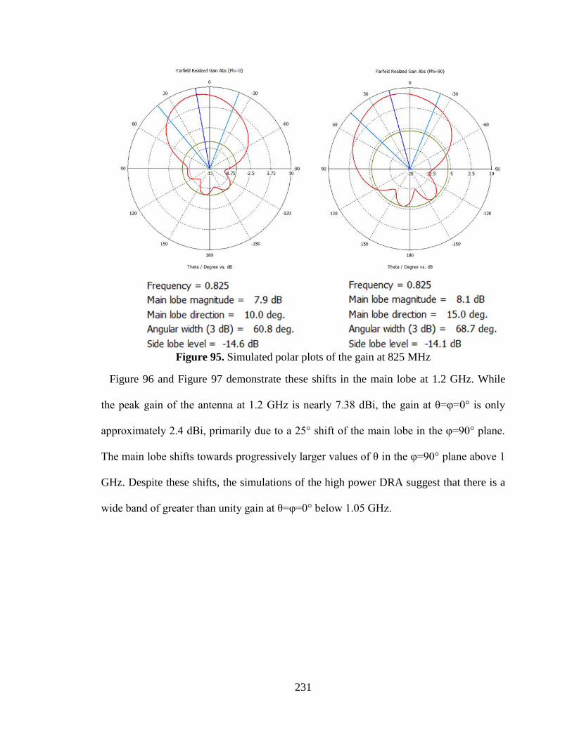
231
Figure 95. Simulated polar plots of the gain at 825 MHz
Figure 96 and Figure 97 demonstrate these shifts in the main lobe at 1.2 GHz. While
the peak gain of the antenna at 1.2 GHz is nearly 7.38 dBi, the gain at θ=φ=0° is only
approximately 2.4 dBi, primarily due to a 25° shift of the main lobe in the φ=90° plane.
The main lobe shifts towards progressively larger values of θ in the φ=90° plane above 1
GHz. Despite these shifts, the simulations of the high power DRA suggest that there is a
wide band of greater than unity gain at θ=φ=0° below 1.05 GHz.

232
Figure 96. Simulated 3D plot of the gain at 1.2 GHz
Figure 97. Simulated polar plots of the gain at 1.2 GHz
5.7.2 Low Power Experimental Results
Figure 98 shows the measured return loss both with and without the dielectric resonator
in place. The effect of the resonator is clearly seen between approximately 475 MHz and
1.5 GHz. Above about 1.5 GHz, the return loss is very similar both with and without the

233
resonator. The resonator significantly improves the impedance match of the antenna
below 1.5 GHz as the return loss is generally below -10 dB down to 475 MHz.
Figure 98. Return loss of the high power DRA with and without the resonator. The
impedance match of the antenna is improved between 475 MHz and 1.5 GHz due to the
addition of the resonator.
Figure 99 plots the simulated and measured return loss for direct comparison. The first
two troughs of the simulated waveform occur at slightly lower frequencies than those
measured experimentally, but in general the measured waveform achieves a lower return
loss. The measured return loss is believed to be better than the simulated return loss due
to the precise tuning that can be done experimentally by moving the resonator along the
microstrip. While the simulated resonator should theoretically be in the same position,
relatively small adjustments to the location of the simulated resonator could provide
improvement to the simulated return loss to the level observed in the experimental
measurement. Tuning capability of the resonator position in CST Microwave Studio is
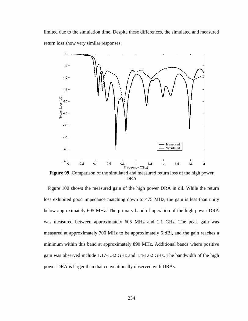
234
limited due to the simulation time. Despite these differences, the simulated and measured
return loss show very similar responses.
Figure 99. Comparison of the simulated and measured return loss of the high power
DRA
Figure 100 shows the measured gain of the high power DRA in oil. While the return
loss exhibited good impedance matching down to 475 MHz, the gain is less than unity
below approximately 605 MHz. The primary band of operation of the high power DRA
was measured between approximately 605 MHz and 1.1 GHz. The peak gain was
measured at approximately 700 MHz to be approximately 6 dBi, and the gain reaches a
minimum within this band at approximately 890 MHz. Additional bands where positive
gain was observed include 1.17-1.32 GHz and 1.4-1.62 GHz. The bandwidth of the high
power DRA is larger than that conventionally observed with DRAs.

235
Figure 100. Measured gain of the high power DRA in oil
Figure 101 compares the measured gain to the gain simulated at θ=φ=0°. The measured
and simulated gains show very similar behavior, and many of the differences below 1
GHz are likely due to slightly shifted maxima in the main lobe of the patterns and
somewhat different return loss values. Both gain profiles show a peak near 475 MHz, but
the measured gain does not extend above unity gain. This discrepancy may be due to
misalignment of the lobe maximum. The gain values are very close between 575 MHz
and 700 MHz as the gain rapidly increases. The measured gain peaks at around 700 MHz,
and the lower gain seen in the measurements between 700 MHz and 975 MHz is also
believed to be due to shifts in the far field gain pattern off axis. The measured gain is
greater than the simulated gain between approximately 975 MHz and 1.1 GHz. Although
the far field gain pattern was not measured in this work, the agreement between the gain

236
measured at θ=φ=0° provides a level confidence that the features of the simulated gain
pattern apply to the constructed antenna.
Figure 101. Comparison of the measured gain and simulated gain at θ=φ=0°
5.7.3 Evaluation of Experimental Results against Fundamental Limits
The measured gain of the high power DRA was compared to the theoretical limits
imposed by Harrington’s derivation. Figure 102 shows a plot of equation (5.25) for
spheres that would approximately circumscribe the dimensions of the DRA substrate and
dielectric resonator. The substrate has side dimensions of approximately 30.48 cm, so a
sphere radius of 15.24 cm was used in the calculated curve. The diameter of the resonator
is approximately 7.62 cm, so a sphere radius of 3.81 cm was used for the second curve.
Due to the thickness of the substrate and resonator, spheres completely circumscribing all
edges of these structures would be slightly larger than the values used in the calculations.

237
However, the effect of increasing the sphere radius by a small amount would slightly
increase the maximum theoretical gain. Therefore, the curves of Figure 102 represent a
slightly underestimated maximum theoretical gain.
As seen in Figure 102, the measured gain is below the theoretical limit. Two important
conclusions can be stated from this result. First, the high power DRA is operating within
the limits of the normal gain for the size of the antenna as established by Harrington.
Second, further antenna minimization through reduction of the substrate and ground
plane is possible. Even if the substrate, ground plane, and feed structure were reduced to
the circular cross-section of the resonator, the same gain profile as that measured with the
large substrate would not be in violation of this practical limit. It should be noted that
other practical limitations may limit the reduction of the DRA to this extent, including
changes to the radiation pattern as a result of significant changes to the ground plane size.
Nevertheless, while the substrate and ground plane size were designed to be relatively
large for the requirements of the experiments in this work, including the need for a large
microstrip feed capacitance, other applications of the DRA could be minimized to much
smaller substrates.

238
Figure 102. Measured DRA gain along with the theorectical maximum normal gain for
antennas enclosed in a sphere around the full DRA substrate and around only the
resonator
239
References for Chapter 5
[1] R. D. Richtmyer, "Dielectric resonators," Journal of Applied Physics, vol. 10, pp.
391-398, 1939.
[2] D. Kajfez and e. P. Guillon, Dielectric Resonators. Norwood, MA: Artech House,
1986.
[3] A. Petosa, Dielectric Resonator Antenna Handbook. Norwood, MA: Artech
House, 2008.
[4] R. A. Krannenburg and S. A. Long, "Microstrip transmission line excitation of
dielectric resonator antennas," Electronics Letters, vol. 24, pp. 1156-1157, 1988.
[5] S. A. Long, M. W. McAllister, and L. C. Shen, "The resonant cylindrical
dielectric cavity antenna," IEEE Trans. on Antennas and Propagation, vol. AP-
31, pp. 406-412, 1983.
[6] K. W. Leung, K. M. Luk, E. K. N. Yung, and S. Lai, "Characteristics of a low-
profile circular disk DR antenna with very high permittivity," Electronics Letters,
vol. 31, pp. 417-418, 1995.
[7] R. K. Mongia, A. Ittibipoon, and M. Cuhaci, "Low profile dielectric resonator
antennas using a very high permittivity material," Electronics Letters, vol. 30, pp.
1362-1363, 1994.
[8] F. T. Ulaby, Fundamentals of Applied Electromagnetics. Upper Saddle River, NJ:
Prentice Hall, 2001.
[9] H. A. Wheeler, "Transmission-line properties of a strip on a dielectric sheet on a
plane," IEEE Trans. on Microwave Theory and Techniques, vol. MTT-25, pp.
631-647, 1977.
[10] K. A. O'Connor and R. D. Curry, "High dielectric constant composites for high
power antennas," in Proc. 18th IEEE Intl. Pulsed Power Conf. Chicago, IL, 2011.
[11] D. Pozar, Microwave Engineering, 3rd ed. Hoboken, NJ: John Wiley and Sons,
2005.
[12] C. Balanis, Antenna Theory: Analysis and Design, 3rd ed. Hoboken, NJ: John
Wiley and Sons, 2005.
[13] "Log-periodic antennas LP80: 80MHz-2GHz LP100:100MHz-2GHz," Sunol
Sciences, Dublin, CA 2012.
[14] M. L. Kales and J. I. Bohnert, "Elliptically polarized waves and antennas," Naval
Research Laboratory, Washington, D.C. 1950.
[15] G. Breed, "Basic principles of electrically small antennas," in High Frequency
Electronics. vol. 6, 2007, pp. 50-53.
[16] J. Volakis, Antenna Engineering Handbook, 4th ed. New York, NY: McGraw-
Hill, 2007.
[17] L. J. Chu, "Physical Limitations of Omnidirectional Antennas," Massachusetts
Institute of Technology 1948.
[18] R. F. Harrington, "On the Gain and Beamwidth of Directional Antennas," IRE
Trans. on Antennas and Propagation, vol. 6, pp. 218-225, 1958.
[19] R. C. Hansen, "Physical Limitations in Antennas," Proc. of the IEEE, vol. 69, pp.
170-182, 1981.

240
Chapter 6: High Power Antenna Driver
6.1 System Overview
A high power antenna driver was developed as a final means of experimentally testing
the high power DRA and future dielectric-loaded antennas. In addition to the requirement
that the antenna developed through this program have reduced dimensions through
incorporation of the high dielectric constant composite material, the antenna is intended
to be capable of transmitting signals at frequencies below 1 GHz at a peak power level on
the order of 1 GW. Thus the antenna driver must be capable of driving the antennas at
frequencies on the order of 100s of MHz to 1 GHz at peak power levels on the order of
10s of MW to 1 GW. The driver was designed to be capable of driving a range of
prospective antenna impedances at 1 GW or greater. The peak voltage requirement for
the antenna driver to achieve 1 GW of applied power can be calculated based on the
impedance of the load. For antenna input impedances of 50 to 377 Ω, the voltage
requirement varies from approximately 223.6 kV to 614 kV, respectively. Since the high
power antenna driver signal applied to the antenna will incorporate significant frequency
content at frequencies below the antenna operation frequencies, the power at the
frequencies of operation of the antenna will be much less than 1 GW. Nevertheless, the
high power antenna driver enables testing of the antenna structures under high peak
power conditions.
Two types of high power antenna drivers were considered in this work. The first type of
high power antenna driver applies a high voltage pulse to the antenna with a very fast
risetime. The frequency content of the signal composing the fast rising voltage signal is

241
spread over a wide band of frequencies, and this type of antenna driver is used in the
research of impulse radiating antennas (IRAs). When a step input with a fast rising edge
is applied to an impulse radiating antenna, the radiated field is the derivative of the
applied voltage signal. Thus, an IRA radiates an impulse in response to the step input [1].
A high voltage step input has also been applied to other antennas, including a high power
helical antenna, under the concept of shock excitation [2]. A Marx generator was
implemented as the high voltage source of a fast risetime single in the helical antenna
investigation [2]. The PA-80 high voltage trigger generator with a peaking switch to
decrease the risetime was considered as a part of this work. While this was determined to
be a viable method for performing high power antenna testing with IRAs or other
antennas in which the time-domain behavior of the antenna is well characterized, it is not
the preferred type of antenna driver for a resonant antenna like a DRA.
The second type of high power antenna driver considered in this study applies a high
voltage damped sinusoidal signal to the antenna under test. This type of antenna driver
was designed, built, and tested in this work. The high power antenna driver was
developed based on a previously investigated system for compact high voltage RF
generation with explosive generators, inductive energy storage, exploding wire fuses, and
compact ring-down oscillators [3, 4]. Significant modifications were made to the system,
including improvement of the simulator of the explosive generator and the capability of
generating higher frequency content in the voltage signal applied to the antenna. The
following section provides an overview of the high power antenna driver with subsequent
sections highlighting new or important design aspects of individual components.

242
The high power antenna driver can be separated into the three subsystems shown in
Figure 103. The subsystems consist of a current source, an inductive energy store, and a
high power ring-down oscillator. The flow chart also follows the path of energy delivered
to the antenna under test as it is delivered from its source, stored in an intermediate
storage element, and diverted to a high power oscillator. The oscillating voltage produced
by the high power oscillator directly drives the high power antenna under test.
Figure 103. Flow chart for the high power antenna driver
The first subsystem serves as the primary energy storage system and current source. A
variety of systems could potentially fulfill the requirements of the current source, but
consideration in this study was limited to a flux compression generator (FCG) or a
simulator of an FCG. In this case, the FCG or FCG simulator provides an approximately
exponentially rising current signal, reaching a peak current on the order of tens of
kiloamps after a risetime on the order of several microseconds. The total electromagnetic
energy output of the FCG or FCG simulator is on the order of kilojoules.

243
The second subsystem, the inductive energy storage system, stores energy delivered by
the source in its magnetic field. Although the requirements of the source and inductive
energy store can vary widely for different systems, the inductance of the storage medium
considered here is typically on the order of 1 µH. For a peak current through this
inductive element on the order of tens of kiloamps, the energy inductively stored can vary
from a few hundred joules up to a few kilojoules. The inductive energy storage
component is typically either a solenoid inductor or the primary winding of a pulse
transformer. Figure 104 displays the schematic for the high power antenna driver. The
inductive storage element is represented in this schematic by the inductor LIS.
The second component of the inductive energy storage system is the opening switch,
which is implemented as an electroexplosive opening switch (EEOS). As the source
produces its rising current signal, most of the current passes through the EEOS,
represented as REEOS in Figure 104. As the EEOS resistance rises, energy is transferred to
charge the capacitance of the transmission lines, represented by components T1 and T2 in
Figure 104, charging them to high voltage.
The third subsystem is a high power oscillator consisting of high voltage capacitive
transmission lines. The high voltage feed to the antenna under test is made between the
two high voltage transmission lines. When the switch S is closed, the transmission lines
are shorted through a shunt inductance, and a series of high voltage oscillations along
with high frequency content from reflections occur due to mismatching of the
transmission lines and antenna impedance. This high power RF signal directly drives the
antenna under test, represented by the antenna’s impedance, ZA. The following two

244
sections describe the design and operation of the driver’s subsystems with emphasis on
the improvements made to the FCG simulator, EEOS, and high voltage oscillator.
Figure 104. Inductive energy storage systems and high power oscillators driving antenna
impedance ZA
6.2 Revised FCG Simulator
6.2.1 Background and Theory of Operation
The FCG simulators have been developed in the last decade primarily as a means for
non-destructive testing of power conditioning components intended for use with FCGs.
Previous work by the author has also investigated the use of an FCG simulator to test
alternative compact RF generators along with power conditioning components for
explosively-driven systems [3, 4]. Although the dielectric-loaded antennas under
development are not limited to explosively-driven systems, the addition of the antennas
to a modified version of the previously developed components completes the system by
radiating the RF signal.
The FCG simulators are distinguished from traditional capacitor-driven sources in that
they attempt to replicate the exponentially rising current waveform characteristic of an
FCG. Whereas a typical capacitive discharge has its greatest rate of current rise at the
very beginning of the discharge, the discharge of an FCG simulator is modified to have
an increasing rate of current rise during its operation. In the past, this effect was mainly

245
achieved through magnetically-switching parallel inductance into the circuit to decrease
the circuit inductance in time [5]. An FCG simulator based upon this principle was
previously utilized with modifications from the original design, including using a
capacitor bank to drive the inductive network rather than a pulse forming network and
lowering the inductance to allow the simulator to drive external inductive and system
loads [6].
The newly modified FCG simulator developed for the high power antenna driver
incorporates two fundamental changes to the previous FCG simulators. Although
magnetically switching parallel inductors into the circuit can provide a stepped effect
increasing the rate of current rise, the decreasing voltage on the capacitor bank or PFN
output in time results in a decreasing rate of current rise between switch closures. A
significant modification to the new FCG simulator is to drive the inductive network with
a rising voltage in time. This is accomplished by driving the inductor network in parallel
with a capacitor-inductor-capacitor (CLC) network, as shown in Figure 105. Capacitor
bank C1 is initially DC charged to high voltage. When the switch S is closed, the voltage
across capacitor bank C2 slowly increases over several microseconds. The rising voltage
across capacitor bank C2 initially drives an increasing current through inductor L1 while
all of the magnetic switches remain closed. The rising voltage across L1 enables the
current through the inductive energy store (IES) to increase smoothly with a derivative
similar to that of an FCG. As the rate in the voltage rise on capacitor C2 reaches its
inflection point and begins to decrease, magnetic switches sequentially close to lower the
circuit inductance in time. The network of inductors is designed such that L1 > L2 > L3 >
L4, and L4 is the minimal inductance achievable to effectively short out the network of

246
inductors at the end of the simulator’s current rise. Magnetic switches LS1 and LS2 were
arranged in the same manner as previous FCG simulators and were designed to close
sequentially. However, unlike the arrangement of previous simulators, magnetic switch
LS3 and inductor L4 now form a parallel path with inductor L1. This improvement was
made to the new simulator to minimize the network’s inductance after the closure of
magnetic switch LS3. Whereas in the previous design the path through the short circuit
inductor L4 would also include the saturated inductances of all three magnetic switches,
the new arrangement only includes the saturated inductance of one magnetic switch.
Additionally, since the network of inductors is driven with the slowly rising voltage
waveform across capacitor C2, the requirements on the size and number of windings on
the magnetic switches are reduced, lowering the saturated inductances of the switches.
The resistor R1 is a low resistance load to dissipate the extra energy in the CLC network
after operation of the FCG simulator is complete.
Figure 105. CLC-Driven FCG Simulator
Figure 106 displays the simulated current output of the revised FCG simulator of Figure
105. Both capacitor banks were defined to be 6.6 µF, and VDC was 35 kV. The values for
R1 and L0 were 0.25 Ω and 5 µH, respectively. The values for inductors L1 – L4 were 10
µH, 10 µH, 1 µH, and 10 nH, respectively. Switches LS1 – LS3 were designed to saturate

247
due to a flux change of 42 mV∙s, 15 mV∙s, and 50 mV∙s, corresponding to closure times
of 8 µs, 9 µs, and 9.5 µs, respectively, after the closure of switch S. The load of the FCG
simulator was a 1 µH inductance with no opening switches in series.
The simulated output of the new FCG simulator produces a current waveform that more
closely resembles an exponential rise than previous simulators. The second derivative of
the current is positive through the first 8 µs of operation as the voltage driving the
inductor network increases. When the magnetic switches begin closing, the first
derivative is increased in large steps to ensure an increased rate of current rise. The
simulator current reaches greater than 40 kA after 10 µs and a peak of approximately 55
kA.
Figure 106. Simulated revised FCG current into 1 uH
6.2.2 Magnetic Switches
One of the critical elements that enable the current of an FCG simulator to be unique
from that of a simple capacitive discharge is the decreasing circuit inductance in time.

248
Magnetic switches have consistently been implemented in FCG simulators for this
purpose [3, 7]. Magnetic switches have been a unique option for transient switching since
first being described in 1951 [8]. Magnetic switches have found widespread application
for laser drivers and accelerators in magnetic pulse compression circuits [9-11]. The
magnetic switches of the FCG simulator enable the sequential switching of the fixed
parallel inductors, L1 - L4 of Figure 105, into the circuit, resulting in a decreasing circuit
inductance in time. A simple magnetic switch can be formed by winding a conductor
around a magnetic core. Current through the winding creates a magnetic field, which is
coupled in the magnetic core. As the magnetic field, H [A/m], is increased, the magnetic
flux density, B [T], increases in response [12]. The magnetic field and the magnetic flux
density are related by the permeability of the magnetic material, µ [H/m]. The
permeability is the product of the permeability of free space, µ0 [H/m], and the relative
permeability of the material, µr. Equation (6.1) shows the relation between the magnetic
flux density, magnetic field, and permeability [13].
(6.1)
A plot of the magnetic flux density versus the magnetic field is known as a hysteresis
loop [13]. The hysteresis loop of a ferromagnetic material is directly analogous to the
hysteresis loop previously discussed for ferroelectric materials. A hysteresis loop for a
ferromagnetic material can demonstrate saturation of the ferromagnetic material. When
the absolute value of the magnetic field in the material is less than the saturation value,
Hsat [A/m], the magnetic field and magnetic flux density have approximately a linear
relation. When below Hsat, a small change in the magnetic field results in a large change
in the magnetic flux density. This response corresponds to a relative permeability with a

249
high value when the magnetic core is in an unsaturated state. When the absolute value of
the magnetic field is greater than a saturation value, Hsat [A/m], the relative permeability
approaches 1, and relatively large changes in the magnetic field produce relatively small
changes in the magnetic flux density. This response corresponds to the saturated state of
the magnetic core. Magnetic switches leverage the difference between the unsaturated
and saturated states of the magnetic core to change the impedance of a winding coupled
to the core material.
A winding around a magnetic core has an inductive impedance directly proportional to
the relative permeability of the magnetic material. The equation for solenoid inductance,
L [H], is given as equation (6.2) [14]. The symbol N represents the number of turns. The
symbol A [m2] is the cross-sectional area or the magnetic core, and the length of the
solenoid is given as l [m].
(6.2)
When the core is unsaturated, the relative permeability is relatively high, and the
inductance of the solenoid is proportionally high. The high impedance of the winding
results in a very slow rate of current rise. If a lower impedance parallel current path is
present, the current path through the winding can approximately be considered to be
open. When the core is saturated, the relative permeability is substantially decreased from
the unsaturated value. The inductance is decreased by order of magnitude. The
corresponding inductive impedance to current in the winding is proportionally decreased
by orders of magnitude, and the current path through the winding can no longer be
considered open. This is the closed state of the magnetic switch. Through this change in
inductive impedance, the magnetic switch operates as a closing switch [15].

250
The design of the magnetic switches in the FCG simulator is primarily dependent
upon the change in flux density in the magnetic core. The change in flux density, ΔB
[Wb/m2], due to a single winding turn is equivalent to the integral of the applied voltage
per unit area. Expressing this relationship mathematically, the required area of the core
can be determined based upon the maximum change in flux density, the number of turns,
and the integral of the applied voltage [10].
(6.3)
The voltage across the inductance is V [V], and the symbol tsat [s] is the time of core
saturation. The number of turns on the core is N, and the area of the core is represented as
A [m2]. Due to the high voltage applied at the beginning of FCG simulator operation, the
cores require a large area and high change in magnetic flux density to remain unsaturated
for a time on the order of microseconds. The number of turns could also be increased.
However, to minimize the saturated inductance of the winding, the number of turns was
minimized. Each of the three magnetic switches was formed from stacks of identical
magnetic cores to increase the cross-sectional area. Magnetic switches LS1 and LS3 were
both constructed with two Metglas AMCC1000 cores [14]. Magnetic switch LS2 was
formed with three square orthonol cores. The parameters of the three saturating magnetic
cores are given in Table 22.
Table 22. Magnetic Core Parameters
Switch N Area A (m2) ΔB (T) Volt-second product (mVs)
LS1 4 0.0023 3 27.6
LS2 2 0.002044 3 12.3
LS3 2 0.0069 3 41.4

251
After operation of the FCG simulator, the cores of the magnetic switches will relax to
a state such that the maximum ΔB to saturation with the next applied voltage is
substantially reduced. Therefore, the cores must be reset, or saturated by a magnetic field
with the opposite polarity, to enable the large change in flux density desired in operation
of the magnetic switch [16]. The minimum reset current, Ireset [A], can be produced in the
magnetic switch winding in the opposite direction as the FCG simulator current, or a
separate winding can be added to the magnetic switch. The reset current is determined by
the number of reset windings, Nr, the magnetic path length of the core, lm [m], and the
saturation magnetic field, Hsat [A/m], as shown in equation (6.4) [16].
(6.4)
The parameters lm and Hsat are dependent upon the magnetic cores. Since the FCG
simulator is not repetitively operated, the number of windings and reset current supply
were not critical design factors. A 25 A DC current supply was used as the reset current
source.
6.2.3 High Power Antenna Driver Construction
Figure 107 shows the constructed CLC-driven FCG simulator. A second view in Figure
108 shows the three levels of components. This structure was designed to allow the
system to fit inside an RF-shielded room while leaving half of the top level open for the
remaining high power antenna driver components. The capacitor banks on the bottom
level were each composed of 3 2.2 µF capacitors rated at 100 kV. The second level of the
FCG simulator included the main spark gap switch for the CLC circuit, the inductor of
the CLC circuit, the low resistance energy dump, and assorted charging and triggering
components. The main switch for the system was a T-670 pancake spark gap pressurized

252
with dry air. The inductor was constructed as an air-core solenoid. The low resistance
energy dump included to safely dissipate energy left in the CLC circuit after system
operation was implemented as five paralleled 1.25 Ω resistors. The top level of
components consisted of the network of inductors and magnetic switches. The inductors
were constructed as air-core solenoids of copper tubing.
Figure 107. CLC-driven FCG simulator during evaluation prior to incorporation into the
high power antenna driver
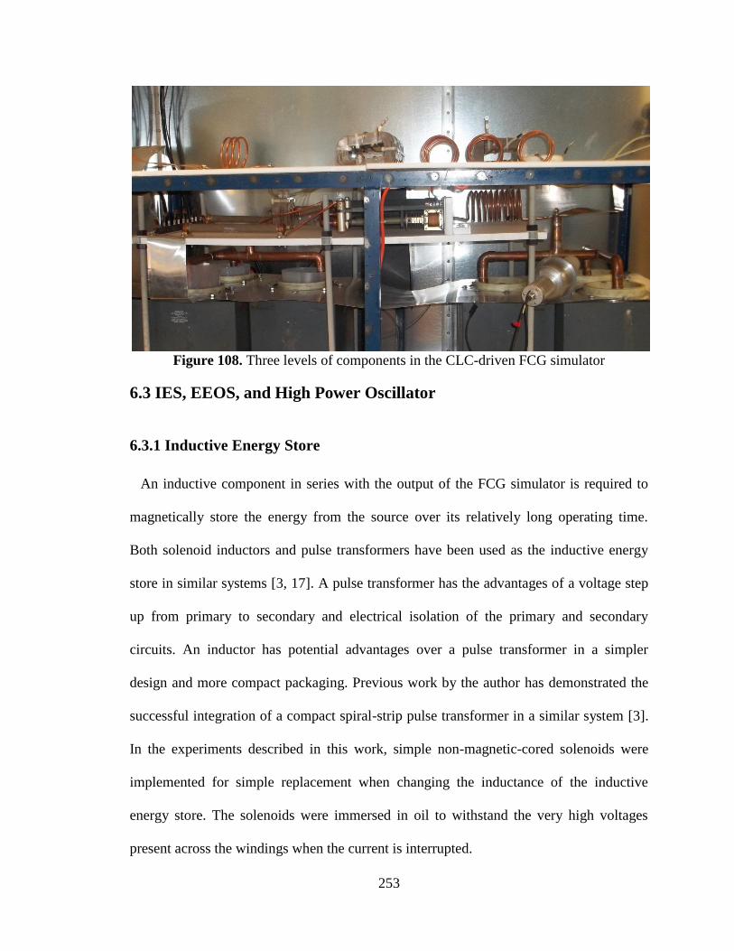
253
Figure 108. Three levels of components in the CLC-driven FCG simulator
6.3 IES, EEOS, and High Power Oscillator
6.3.1 Inductive Energy Store
An inductive component in series with the output of the FCG simulator is required to
magnetically store the energy from the source over its relatively long operating time.
Both solenoid inductors and pulse transformers have been used as the inductive energy
store in similar systems [3, 17]. A pulse transformer has the advantages of a voltage step
up from primary to secondary and electrical isolation of the primary and secondary
circuits. An inductor has potential advantages over a pulse transformer in a simpler
design and more compact packaging. Previous work by the author has demonstrated the
successful integration of a compact spiral-strip pulse transformer in a similar system [3].
In the experiments described in this work, simple non-magnetic-cored solenoids were
implemented for simple replacement when changing the inductance of the inductive
energy store. The solenoids were immersed in oil to withstand the very high voltages
present across the windings when the current is interrupted.

254
6.3.2 Electroexplosive Opening Switch
A required component in inductive energy storage systems is an opening switch. The
opening switch serves to redirect the current from the low impedance path through it
while storing the energy inductively to the higher impedance path of the load to the
inductive energy storage system. A wide variety of opening switches have been
developed for specific conditions. For the high power antenna driver, which requires high
currents of tens of kiloamps to be conducted for several microseconds before the current
is interrupted in a period of less than one microsecond, the best available opening switch
is the electroexplosive opening switch (EEOS) [18]. An EEOS can take the form of an
exploding wire fuse or an exploding foil.
An EEOS transitions from a closed to open state through a fast increase of the
resistance of its conducting element, either wires or a foil, as the element vaporizes.
While the initial cold resistance of the EEOS is often on the order of milliohms, the
resistance as the metal vaporizes can rise to several ohms or higher, depending on the
dimensions of the EEOS. If enough energy is dissipated in the EEOS after the onset of
vaporization, a combination of factors, including expansion of the EEOS conducting
material, the electric field across the EEOS, and ionization of the vaporized material can
cause the resistance of the EEOS to drop significantly. This drop in EEOS resistivity is
commonly termed restrike. In nearly all previously-developed inductive energy storage
systems developed, it has been desirable to avoid restrike throughout the system’s
operation as restrike in those systems represented a failure of the opening function of the
switch.

255
Although restrike causes an EEOS to no longer function as an opening switch, it was
noted in a publication on a previous iteration of this type of antenna driver that by the
time restrike occurred, the inductive energy storage system had already driven the high
power oscillator [19]. The occurrence of restrike did not degrade the operation of that
system, but restrike did occur due to inefficiencies in the system. While it was previously
noted that these inefficiencies could be eliminated by either driving the system with a
lower energy source or driving the load to a higher voltage, a previously-unmentioned
third option of driving the load multiple times forms the basis of the approach taken in
this system [19].
The time at which an EEOS begins to vaporize is determined using the integral of
current action through the EEOS, and the integral of current action at which the EEOS
vaporizes can be modified by changing the cross-sectional area of the EEOS conducting
medium. Equation (6.5) shows the determination of the integral of current action, h [A2s],
where t0 [s] is the time at which current begins flowing through the EEOS.
(6.5)
The action limit, he [A2s], is determined by applying equation (6.5) with the limits of the
integral from the beginning of current flow to the time at which the EEOS begins to
vaporize and its resistance dramatically increases. The cross-sectional area of the EEOS,
A [m2], can be related to the integral of current action at the time at which the EEOS
begins to vaporize through equation (6.6) [3]. The symbol αl [m2/(A∙s
0.5)] is a factor
dependent on the materials used and experimental conditions, including the current
density and rate of energy dissipation [20]. Values of αl have been experimentally
determined for specific materials [20].

256
(6.6)
Figure 109 shows the electroexplosive opening switch, which was implemented as an
exploding wire fuse. The switch consists of two sections approximately 12.7 cm each.
The fusing element was composed of 40 gauge silver-plated copper wire. The typical
number of wires ranged from 15 to 30, depending on the desired action integral at which
the fuse was intended to open. The entire assembly was packed in fine glass beads with a
rated mesh size of 170-325 to act as a quenching material. Additional details about the
exploding wire fuse and analysis of electroexplosive opening switches has been
previously published by the author [3, 21, 22].
Figure 109. Two-section exploding wire fuse
6.3.3 High Power Oscillator
In the previous version of a high power oscillator driven by an FCG and inductive
energy storage system, a high voltage capacitor was charged as the EEOS vaporized until
a self-breaking switch closed to form an underdamped oscillator with a low inductance
shunt [3, 19]. The operation of the oscillator in this work is similar, but the capacitive
element is formed from two high voltage coaxial sections. Both the capacitance and
transit time of the transmission line are important to the operation of the oscillator. The

257
primary function of the element is to serve as the capacitive component of the oscillator.
However, due to the low inductance of the circuit when the capacitance is shorted, the
transmission line effects of the capacitor cannot be ignored. The reflections from the
terminals of the capacitive transmission line can benefit the system by enabling a broader
and higher range of frequencies to be applied to the high power antenna. While the two
transmission line sections are identical, reflections between the sections are enhanced by
feeding the antenna impedance at the junction of the transmission line sections. The
microstrip feed of the antenna also acts as a transmission line, introducing additional
reflections. The multiple reflections between these short transmission lines cause the
frequency content of the signal at the antenna input to spread to much higher frequencies
than a simple resonator formed by a capacitance ringing into the inductance of a closing
switch.
As shown in Figure 110, the high voltage capacitive transmission lines were
constructed from coaxial cylinders of copper. The impedances of the lines were kept low
to increase capacitive energy storage while ensuring that they can withstand pulsed
voltages on the order of hundreds of kilovolts. The transmission lines are insulated in oil
to increase their breakdown strength. The plastic insulators shown in Figure 110 provided
mechanical stability to the positioning of the inner cylinders within the grounded outer
cylinders. A subsequent modification extended the plastic supports out from the sides of
the structure to remove the plastic rods from the high electric field region. This
modification prevented surface tracking along the plastic rods.
The outer diameter of the inner copper pipes of the coaxial structures was
approximately 19.05 mm, and the inner diameter of the outer copper pipes of the coaxial
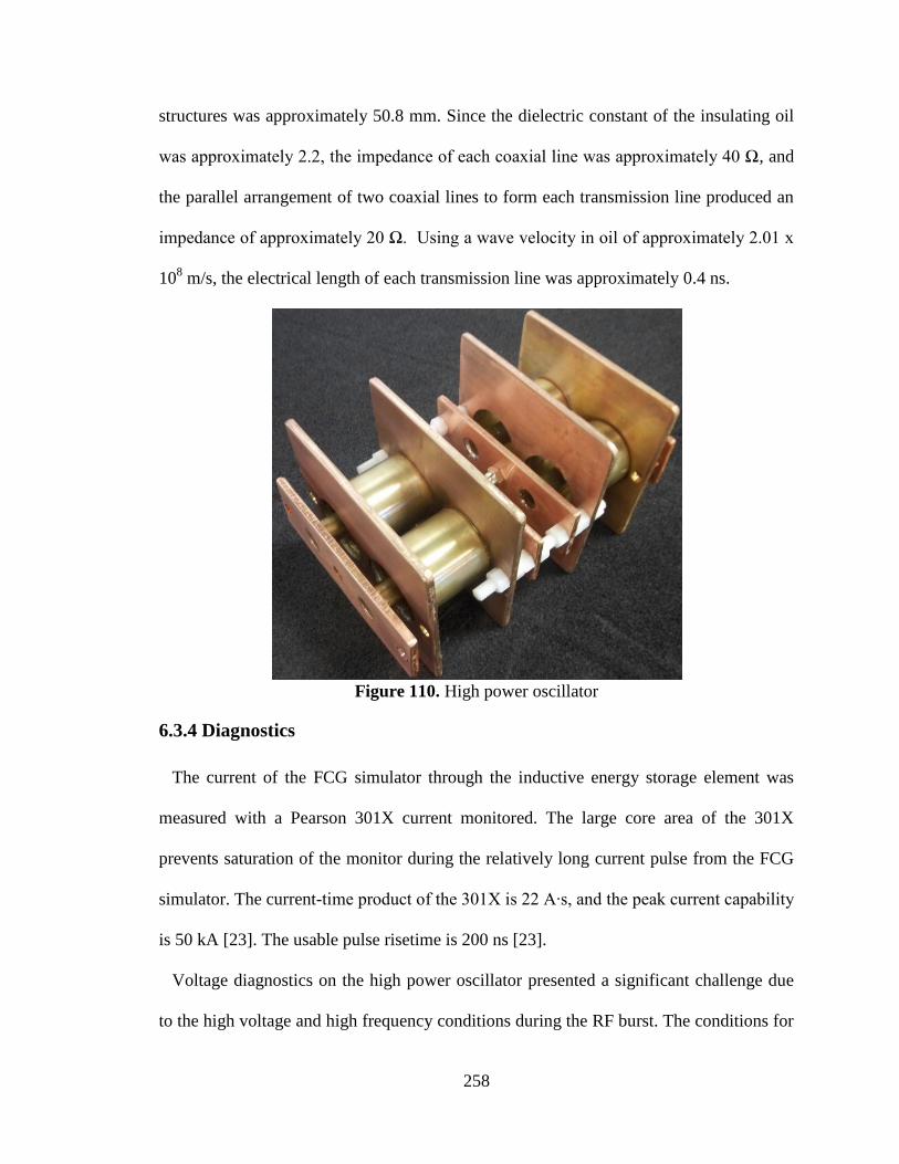
258
structures was approximately 50.8 mm. Since the dielectric constant of the insulating oil
was approximately 2.2, the impedance of each coaxial line was approximately 40 Ω, and
the parallel arrangement of two coaxial lines to form each transmission line produced an
impedance of approximately 20 Ω. Using a wave velocity in oil of approximately 2.01 x
108 m/s, the electrical length of each transmission line was approximately 0.4 ns.
Figure 110. High power oscillator
6.3.4 Diagnostics
The current of the FCG simulator through the inductive energy storage element was
measured with a Pearson 301X current monitored. The large core area of the 301X
prevents saturation of the monitor during the relatively long current pulse from the FCG
simulator. The current-time product of the 301X is 22 A∙s, and the peak current capability
is 50 kA [23]. The usable pulse risetime is 200 ns [23].
Voltage diagnostics on the high power oscillator presented a significant challenge due
to the high voltage and high frequency conditions during the RF burst. The conditions for
259
measurement of the RF burst were contrasted by the relatively slow change in voltage
during charging of the high power oscillator. Since the peak voltage on the high power
oscillator can exceed 100 kV and the frequencies in the voltage signal extended well
above 80 MHz, commercial high voltage probes based on compensated resistive dividers,
such as the PVM-6, were incapable of meeting the measurement requirements. Thus,
custom D-dot probes were added to the high voltage oscillator to monitor the voltage
along the coax sections near the feed to the antenna. The D-dot probes were fabricated by
drilling holes into the outer ground cylinder of each high voltage transmission line
section. The flanged connectors for coaxial cables were mounted on the holes with the
open faces of the modified connectors pointed towards the inner cylinder of the high
voltage transmission lines. The signal of the D-dot probes was proportional to the
derivative of the voltage on the transmission lines. The D-dot probes were calibrated by
applying a fast-rising pulse to the high voltage transmission lines with a Tektronix Type
109 Pulse Generator with a risetime rated at less than 0.25 ns. Figure 111 shows an
example of the signal obtained with the custom D-dot probe, and Figure 112 shows the
pulse obtained by integrating the signal of Figure 111 and scaling the amplitude to match
the directly measured from the Type 109 Pulse Generator. The large scaling factor on the
order of 5.3 x 10¹¹
and the use of attenuators were necessary to be able to measure the
large voltage derivative, which is on the order of 10s of TV/s. However, this scaling
provided a relative lack of sensitivity for the comparatively low voltage derivative during
pulse charging of the high voltage oscillator.
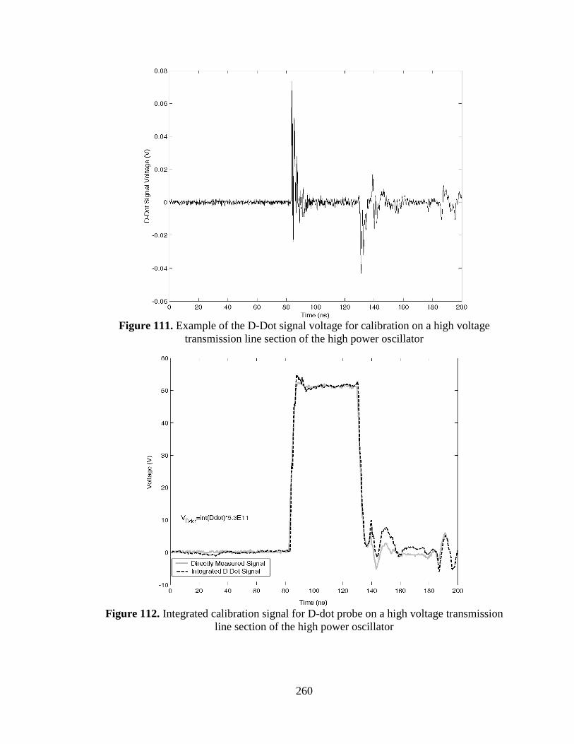
260
Figure 111. Example of the D-Dot signal voltage for calibration on a high voltage
transmission line section of the high power oscillator
Figure 112. Integrated calibration signal for D-dot probe on a high voltage transmission
line section of the high power oscillator

261
Due to the high power radiated fields anticipated from this system, it was contained in
an RF-shielded chamber to protect sensitive equipment in the laboratory. Due to the
dimensions of the chamber and the lack of adequate anechoic material to limit internal
field reflections, it was not possible to evaluate the antenna’s performance during these
initial tests of the high power antenna driver. However, the fields produced by the high
power DRA and the test stand driving it were monitored to measure the peak field
strength and frequency content of the fields within the chamber. These measurements
were made with a NanoFast 709-2B E-field monitor and a Fischer Custom
Communications F301 H-field monitor. The E-field monitor was rated at 10 kV/m and
featured an integrated optical signal transmission system. The use of a fiber optic signal
carrier rather than a coaxial cable eliminates the disturbance of the E-field due to coaxial
cables and ground loop effects in the signal. The NanoFast E-field monitor was placed
approximately 1.5 m above the DRA, and the F301 H-field monitor was placed in the
near field of the antenna.
6.4 High Power Antenna Driver Simulations
Simulations were run on an inductive storage system, repetitively-opening switch, and
transmission line-based high voltage capacitor. An initial current of 40 kA was assigned
to an inductive energy storage inductance of 2 µH. Referencing Figure 104, both
transmission lines were defined to have characteristic impedances of 100 Ω and transit
times of 0.5 ns. The switch representing the exploding wire fuse was defined to increase
from 400 mΩ to 10 Ω in 300 ns. A series resistance, R in Figure 104, was defined to be
700 Ω. The high power DRA was represented as a lossy transmission line with one end
terminated into a high impedance simulating the open end of the microstrip. A switch

262
performing the function of the switch S in Figure 104 was set to short the high power
oscillator into a shunt inductance of 10 nH at 300 ns into the simulation.
Figure 113 displays the simulated voltage waveform at the antenna. The transmission
lines representing the high power oscillator and the microstrip of the high power DRA
were charged to approximately 250 kV in the 300 ns opening time of the simulated
opening switch. Upon shorting the high power oscillator, the first negative voltage peak
occurs at nearly -200 kV. The primary oscillations in the signal are quickly damped by
the lossy transmission line representing the high power DRA. Figure 114 shows a
detailed view of the high frequency content superimposed on the larger voltage
oscillations as a result of reflections along the short transmission lines.
Figure 113. Full view of simulated voltage at antenna input from high voltage oscillator
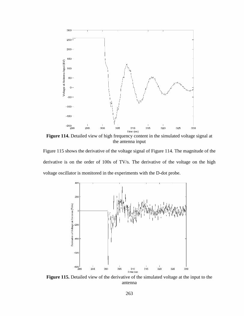
263
Figure 114. Detailed view of high frequency content in the simulated voltage signal at
the antenna input
Figure 115 shows the derivative of the voltage signal of Figure 114. The magnitude of the
derivative is on the order of 100s of TV/s. The derivative of the voltage on the high
voltage oscillator is monitored in the experiments with the D-dot probe.
Figure 115. Detailed view of the derivative of the simulated voltage at the input to the
antenna
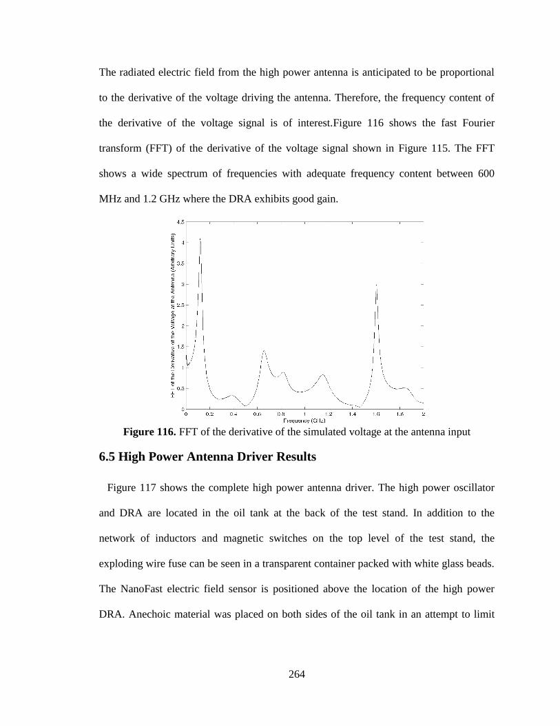
264
The radiated electric field from the high power antenna is anticipated to be proportional
to the derivative of the voltage driving the antenna. Therefore, the frequency content of
the derivative of the voltage signal is of interest.Figure 116 shows the fast Fourier
transform (FFT) of the derivative of the voltage signal shown in Figure 115. The FFT
shows a wide spectrum of frequencies with adequate frequency content between 600
MHz and 1.2 GHz where the DRA exhibits good gain.
Figure 116. FFT of the derivative of the simulated voltage at the antenna input
6.5 High Power Antenna Driver Results
Figure 117 shows the complete high power antenna driver. The high power oscillator
and DRA are located in the oil tank at the back of the test stand. In addition to the
network of inductors and magnetic switches on the top level of the test stand, the
exploding wire fuse can be seen in a transparent container packed with white glass beads.
The NanoFast electric field sensor is positioned above the location of the high power
DRA. Anechoic material was placed on both sides of the oil tank in an attempt to limit

265
the reflected signals observed by the RF sensors and to dissipate some of the energy
radiated by the antenna and test stand.
Figure 117. Fully-integrated high power antenna driver in RF-shielded chamber
6.5.1 CLC-Driven FCG Simulator
Prior to testing the fully integrated high power antenna driver, the operation of the
CLC-driven FCG simulator was evaluated. The exploding wire fuse, high power
oscillator, and DRA were not included in these initial tests. The load of the FCG
simulator was a 1 µH air-core inductor. The charging voltage of capacitor bank C1 in this
experiment was 35 kV. Figure 118 shows the output current signal into the 1 µH load.
The slope of the current rise exhibits the desired concave up shape through the first
several microseconds before gradually leveling off. The peak current reached 40.8 kA at
approximately 14 µs into the waveform. To quantify the analysis of the rate of current

266
rise, a waveform was generated to fit the curve in Matlab. The curve-fit waveform is
shown as the dashed line in Figure 118.
Figure 118. Output current of the CLC-driven FCG simulator into an inductive load
The derivative of the curve-fit waveform of the FCG current is shown in Figure 119. The
derivative reaches a maximum of approximately 5.3 kA/µs at 8.86 µs into the signal. The
decrease of the first derivative of the current signal in the first microsecond of the
simulation is believed to be an artifact of the inaccuracy of the curve fit to the waveform
at time close to t = 0. It is believed that the actual first derivative is positive throughout
the time of interest in the first 10 µs of operation.
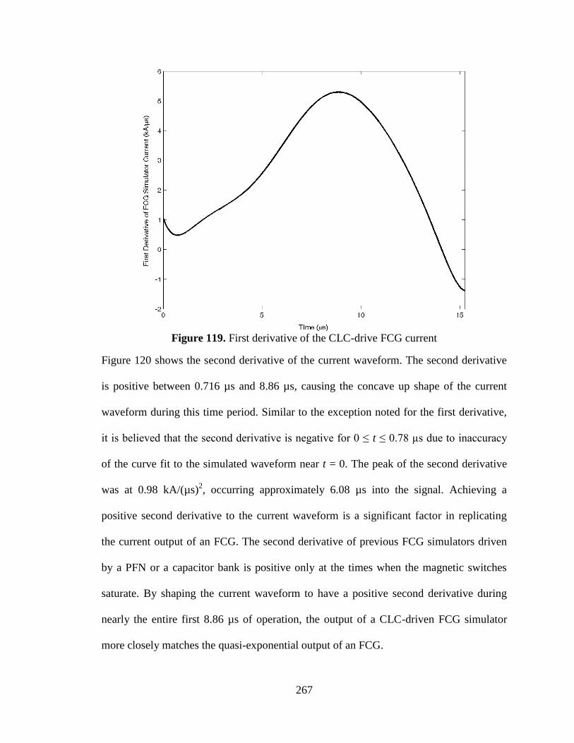
267
Figure 119. First derivative of the CLC-drive FCG current
Figure 120 shows the second derivative of the current waveform. The second derivative
is positive between 0.716 µs and 8.86 µs, causing the concave up shape of the current
waveform during this time period. Similar to the exception noted for the first derivative,
it is believed that the second derivative is negative for 0 ≤ t ≤ 0.78 µs due to inaccuracy
of the curve fit to the simulated waveform near t = 0. The peak of the second derivative
was at 0.98 kA/(µs)2, occurring approximately 6.08 µs into the signal. Achieving a
positive second derivative to the current waveform is a significant factor in replicating
the current output of an FCG. The second derivative of previous FCG simulators driven
by a PFN or a capacitor bank is positive only at the times when the magnetic switches
saturate. By shaping the current waveform to have a positive second derivative during
nearly the entire first 8.86 µs of operation, the output of a CLC-driven FCG simulator
more closely matches the quasi-exponential output of an FCG.

268
Figure 120. Second derivative of the CLC-driven FCG simulator current
6.5.2 Complete High Power Antenna Driver
Preliminary testing was completed on the fully integrated high power antenna driver
with the high power DRA. While testing in the RF-shielded enclosure did not allow the
high power characteristics of the antenna to be evaluated, these tests provided
information on the feasibility of using the system to conduct high power antenna testing.
The results of these tests provide a path forward for full power antenna characterization
in either an anechoic chamber or outdoor range. These tests also provided a means to
demonstrate the high voltage holdoff of the DRA.
In the experiment reported here, the capacitor bank C1 was charged to approximately 40
kV. The exploding wire fuse consisted of 34 40-gauge wires. Figure 121 displays the
FCG simulator current output into the inductive energy storage element and
electroexplosive opening switch. The concave up shape of the current waveform is

269
evident for the first several microseconds even with the added resistive load of the
opening switch. The FCG simulator current reached a peak of nearly 32.8 kA after a
risetime of approximately 13.25 µs. As the current was interrupted due to the rapid
increase in the resistance of the electroexplosive opening switch, the RF signal present
within the shielded enclosure from operation of the high power oscillator is believed to
have coupled to the current monitor and/or signal cable, resulting in the brief burst of
noise present in the current waveform. The current was reduced to below 25 kA in less
than 300 ns before the onset of the RF noise indicating the operation of the high power
oscillator.
Figure 121. Current output of the FCG simulator into the inductive load and
electroexplosive opening switch
Figure 122 shows the voltage signal calculated by integrating the D-dot signal from the
high power oscillator near the feed point to the DRA. The discrepancy between the
timing of the decrease of the current in Figure 121 and the increase in the voltage on the

270
high power oscillator in Figure 122 is due to the signals being measured on different
oscilloscopes, and it should be noted that these events happen concurrently. Due to the
lack of sensitivity of the D-dot probe to the relatively small dV/dt during early stages of
the system’s operation, the peak charging voltage reached on the high power oscillator
and antenna are not definitively known. The voltage displayed in Figure 122 was
obtained by normalizing the mid-point of the initial oscillations to zero volts. This is
considered a reasonable assumption since the voltage should oscillate with respect to
ground after the high power oscillator is shorted. The peak-to-peak voltage from the
maximum charge voltage to the maximum negative trough is approximately 70 kV.
Figure 123 provides a detailed view of the first high power oscillations, showing the high
frequency content of the signal.
Figure 122. Integrated D-dot signal with high frequency oscillations normalized to zero
volts

271
Figure 123. Detailed view of the first high power oscillations near the antenna feed
Figure 124 shows the FFT of the voltage signal of Figure 123. The highest frequency
peak in the frequency content of the signal occurs at approximately 250 MHz.
Figure 124. FFT of the voltage near the antenna feed

272
Figure 125 shows the scaled D-dot signal used to produce Figure 122 and Figure 123.
The D-dot signal can be directly analyzed to determine the frequency content expected in
the radiated field of an antenna that radiates the derivative of the applied voltage.
Figure 125. A plot of the D-dot signal on the high voltage oscillator near the antenna
feed point
Figure 126 is a plot of the FFT of the D-dot signal of Figure 125. There is a substantial
spread in the frequency content between 1 and 2 GHz. As expected, the highest signal
content is below 500 MHz, corresponding to the high voltage oscillations of the shorted
capacitance of the high power oscillator.

273
Figure 126. The FFT of the D-dot signal near antenna feed point
The results of this antenna driver testing indicate that the high power antenna driver
based on a high voltage sinusoidal decay is best suited for use with antennas transmitting
in the VHF band. This type of antenna driver could also potentially drive antennas that
radiate the derivative of the applied voltage at lower peak power levels in the UHF band.
Further investigation is needed on the time-domain behavior of the antennas to be tested
at high power to select the appropriate type of antenna driver and tune the applied
frequency to the degree possible. A path forward has been established to transition this
high power antenna driver to enable antenna characterization in the anechoic chamber, as
described in Section 7.3.

274
References for Chapter 6
[1] M. J. Baretela and J. S. Tyo, "Selectrive trimming of impulse radiating antenna
apertures to increase prompt radiated field," Sensor and Simulation Notes, pp. 1-
27, Note 461, 2001.
[2] J. R. Mayes, M. G. Mayes, W. C. Nunnally, and C. W. Hatfield, "Helical antennas
for high powered RF," in Proc. of the 2009 IEEE Int'l Pulsed Power Conference
Washington, D.C., 2009, pp. 484-488.
[3] K. A. O'Connor, "Compact Power Conditioning and RF Systems for a High
Power RF Source," M.S. Thesis, Elec. and Comp. Engr.,University of Missouri-
Columbia, Columbia, MO, 2008.
[4] L. L. Altgilbers, A. S. Stults, M. Kristiansen, A. Neuber, J. Dickens, A. Young, T.
Holt, M. Elsayed, R. Curry, K. O'Connor, J. Baird, S. Shkuratov, B. Freeman, D.
Hemmert, F. Rose, Z. Shotts, Z. Roberts, W. Hackenberger, E. Alberta, M. Rader,
and A. Dougherty, "Recent advances in explosive pulsed power," Journal of
Directed Energy, vol. 3, 2009.
[5] D. Belt, "Non-explosive test bed for flux compression generator fuses," M.S.
Thesis, Elec. and Comp. Engr., Texas Tech University, Lubbock, TX, 2006.
[6] K. A. O'Connor, R. D. Curry, and L. Altgilbers, "Investigation of a high voltage,
high frequency power conditioning system for use with flux compression
generators," in Proc. 16th IEEE International Pulsed Power Conference and 34th
IEEE International Plasma Science Conf. vol. 2, E. Schamiloglu and F. Peterkin,
Eds. Albuquerque, NM, 2007, pp. 1356-1359.
[7] D. Belt, J. Mankowski, A. Neuber, J. Dickens, and M. Kristiansen, "Design and
implementation of a flux compression generator nonexplosive test bed for
electroexplosive fuses," Review of Scientific Instruments, vol. 77, pp. 094702-1 -
094702-7, 2006.
[8] W. S. Melville, "The use of saturable reactors as discharge devices for pulse
generators," IEE Proceedings (London), Part 3: Radio and Communication, vol.
98, pp. 185-207, 1951.
[9] H. C. Kirbie, M. A. Newton, and P. D. Siemens, in International Magnetic Pulse
Compression Workshop. vol. 2, 1991, p. 341.
[10] W. C. Nunnally, "Stripline magnetic modulators for lasers and accelerators," in
Proc. 3rd IEEE International Pulsed Power Conference Albuquerque, NM, 1981,
pp. 210-213.
[11] D. Birx, E. Cook, S. Hawkins, S. Poor, L. Reginato, J. Schmidt, and M. W. Smith,
"Magnetic switching, final chapter book I: the ATA upgrade prototype,"
Lawrence Livermore National Laboratory, Livermore, CA 1983.
[12] D. J. Craik and R. S. Tebble, Ferromagnetism and Ferromagnetic Domains vol.
4. New York, NY: John Wiley and Sons, Inc., 1965.
[13] F. T. Ulaby, Fundamentals of Applied Electromagnetics. Upper Saddle River, NJ:
Prentice Hall, 2001.
[14] F. W. Grover, Inductance Calculations, Working Formulas and Tables. New
York: D. Van Nostrand, 1946.
[15] W. C. Nunnally, "Magnetic switches and circuits," in Pulsed Power Lecture
Series: Texas Tech University, 1981.

275
[16] D. M. Barrett, "Core reset considerations in magnetic pulse compression
networks," in Proc. of 10th IEEE International Pulsed Power Conference. vol. 2,
1995, pp. 1160-1165.
[17] M. Giesselmann, J. Zhang, T. Heeren, E. Kristiansen, J. Dickens, D. Castro, D.
Garcia, and M. Kristiansen, "Pulse power conditioning with a transformer for an
inductive energy storage system," in Proc. 12th IEEE International Pulsed Power
Conference Monterey, CA, 1999.
[18] K. H. Schoenbach, M. Kristiansen, and G. Schaefer, "A review of opening switch
technology for inductive energy storage," Proc. of the IEEE, vol. 72, pp. 1019-
1040, 1984.
[19] K. A. O'Connor and R. D. Curry, "Experimental results of a high voltage
wideband load driven by a pulse transformer and opening switch power
conditioning system," in Conf. Rec. of the 2008 28th IEEE International Power
Modulator Symposium Las Vegas, NV, 2008, pp. 185-188.
[20] T. Heeren, "Power conditioning for high voltage pulse applications," Ph.D.
Dissertation, Elec. and Comp. Engr.,Texas Tech University, Lubbock, TX, 2003.
[21] K. A. O'Connor and R. D. Curry, "The effects of length on electroexplosive
opening switch resistance," Journal of Applied Physics, To be published, under
review 2011.
[22] K. A. O'Connor and R. D. Curry, "A method for numerically modeling a power-
conditioning system with an electroexplosive opening switch," IEEE Trans. on
Plasma Science, vol. 38, pp. 2520-2530, 2010.
[23] "Pearson Current Monitor Model 301X," Pearson Electronics, Inc., Palo Alto, CA
1999.

276
Chapter 7: Summary and Future Work
7.1 Composite Development and Characterization
7.1.1 Summary
Three classes of high dielectric constant composite materials were developed through
this work. One of the fundamental principles behind the development the high dielectric
constant composites was that the volumetric content of the highest dielectric constant
component materials should be maximized while maintaining robust mechanical
properties. In all three composite classes, the volumetric content of ferroelectric ceramics
was increased through a trimodal distribution of particle sizes designed to increase the
ceramic particle packing density. While MU45 took a conventional approach to creating
a high dielectric constant composite by incorporating a polar polymer with the ceramics,
MU100 and MU550 were designed with innovative concepts to minimize the volume
percentage of binder in the composite.
MU100 employed coupling agents, which are conventionally used only to functionalize
the surfaces of the ceramic particles, as the sole binder for the composite. The coupling
agents form a polysilsesquioxane binder through an in-situ polymerization process after
the ceramic components of the composite have been pressed to their final density. The in-
situ polymerization of a polysilsesquioxane minimizes any increase to the composite
volume due to the addition of the binder while allowing the network formed by the
polysilsesquioxiane to fill the voids between particles. Since the polysilsesquixane

277
directly bonds to the surfaces of the ceramic particles, the composite exhibits good
mechanical strength with a relatively low amount of binder.
MU550 leveraged the unique properties of gelling, thermoreversible biopolymers as the
binder material. Since the composite was pressed to a high density while the biopolymers
were in a solution with a water solvent, excess binder was easily removed from the
composite, limiting the increase to the composite volume due to the addition of the
binder. Upon cooling of the composite, the biopolymers formed fibers based on helical
structures, creating a gel with the remaining water. This gel could then be dehydrated
without collapse of the binder network due to the mechanical integrity imparted by the
dense packing of the ceramic particles. The dehydrated gel formed a network of channels
throughout the ceramic particles through which other fluids could flow. With the
selection of a high dielectric constant fluid filler, the voids within the composite were
filled in a manner that both increases the dielectric strength of the composite while also
significantly increasing the dielectric constant. This concept can be expanded to use of
other fluid fillers, allowing the dielectric constant and losses of the composite to be
relatively easily adjusted.
Multiple methods were used to characterize the three classes of composite materials,
enabling evaluation of the composites against the goals established in Chapter 1. The
dielectric constant and losses were primarily measured through dielectric spectroscopy
with supplemental information provided by polarization measurements and measurement
of high voltage discharges of capacitors formed with the composites. At the low
frequency end of the frequencies of interest for antenna operation between 200 MHz and
4.5 GHz, the dielectric constants of the composites correspond with their namesake
278
values of 45, 100, and 550. MU45 and MU100 exhibit modest dispersion in the dielectric
constant as the measurements decrease to approximately 40 and 90 at 4.5 GHz,
respectively. The dielectric losses remained at or below 0.1 for MU45 and MU100 up to
approximately 2 GHz and 1.75 GHz, respectively. The losses of MU100 remained below
0.1 except for two peaks centered at approximately 1.75 and 2.75 GHz. While these
losses could be further decreased with modification to the ceramic content, losses below
0.1 allowed the composites to be integrated into dielectric-loaded antennas. Due to the
selection of the ceramic and binder materials incorporated into MU45 and MU100, very
little change was observed in the permittivity of these composites at high frequency as a
function of temperature between -20 C and 120 C.
MU550 was designed to maximize the dielectric constant, resulting in a maximum
value of approximately 550 at 200 MHz. The use of a high dielectric constant liquid filler
contributed significant dispersion to the dielectric constant as the value was observed to
decrease to less than 400 at 4.5 GHz. The losses are also increased through the use of a
highly polar liquid filler, and the losses of MU550 are below 0.1 only at frequencies less
than 500 MHz. Observations of the change in the permittivity of the high dielectric
constant liquid filler suggest that MU550 may be best suited for low frequency and high
temperature antenna applications due to the lower dispersion and losses of the liquid filler
at high temperature. While MU550 has not yet been implemented in an antenna, the
concepts behind its structure allow the composite to be relatively easily modified to
decrease the dispersion and dielectric losses, as described in the next subsection.
Dielectric constant measurements obtained through polarization and high voltage
capacitive discharge methods provide insight into the low frequency properties of the

279
composites under high electric field conditions. In both methods, the dielectric constant is
increased in comparison to the value measured through dielectric spectroscopy. This
increase is partially due to the elimination of air gaps along the measurement surface due
to the direct application of sputtered electrodes to the composite surfaces. The dielectric
constant is also increased due to the lower measurement frequency and the higher electric
field within the composite. At low electric fields and a frequency of 100 Hz, the dielectric
constant of MU45 observed from polarization measurements was approximately 109. At
relatively high electric fields around 2 MV/m, the dielectric constant of MU45 was
measured with the polarization and high voltage capacitive discharge methods to be
approximately 209 and 200, respectively. Increasing the electric field further to levels
greater than 6 MV/m resulted in a polarization measurement of the dielectric constant of
MU45 at approximately 324. Similar behavior of the dielectric constant increasing with
higher electric field levels was observed with MU100. While the dielectric constant
observed from low electric field polarization measurements of MU100 was
approximately 135.4, the dielectric constant increased to values of approximately 308.5
and 387.6 at electric field strengths on the order of 4 MV/m and 10 MV/m respectively.
This increase in the dielectric constant of MU100 under high electric field conditions was
also observed through high voltage capacitive discharge measurements. The dielectric
constant was calculated to be approximately 345 when discharged from a charging
voltage corresponding to an electric field of approximately 1.575 MV/m. The change in
the effective dielectric constant with the applied field is consistent with the behavior of
capacitors incorporating high dielectric constant ceramics. To account for this
dependence on the electric field, the composites should be characterized on a case-by-

280
case basis under conditions similar to those that will be encountered during application in
specific antenna designs.
The dielectric strength of the composites was measured under pulsed conditions with a
risetime on the order of tens of nanoseconds. This method most closely replicates the
high dV/dt conditions of use in a high power antenna application. The samples were
prepared with sputtered platinum electrodes covered with a conductive epoxy paste to
minimize the effects of imperfect electrode-composite contact and potential erosion and
pitting of the electrode surface after each test. For comparison with a common low
dielectric constant high voltage insulator, measurements were also taken on Teflon
samples prepared with the same electrodes. Half of the high dielectric constant composite
samples were treated with a high dielectric constant coating around the electrode edge in
an attempt to reduce the field enhancement factor due to the triple point at the electrode
edge. The electric field at breakdown in the untreated samples was examined both with
and without inclusion of the field enhancement factor. When the field enhancement factor
is not considered, the reported electric field corresponds to the field within the bulk of the
material away from the electrode edges. The electric field in the bulk material with no
coating calculated for 1% probability of breakdown through Weibull analysis was 7.17,
38.84, 27.35, and 69.87 MV/m for MU45, MU100, MU550, and Teflon, respectively.
When including the simulated field enhancement factor around the electrode-composite
junction, the peak electric field calculated for 1% probability of breakdown increased to
85.87, 316.53, 175.07, and 193.32 MV/m for MU45, MU100, MU550, and Teflon,
respectively. If dielectric breakdown in the composites is dominated by the effects of the
electrode contact, antenna designs in which the conductor does not directly contact the

281
high dielectric constant material may be able to utilize the composites at electric fields in
the bulk of the material up to these peak magnitudes. For antenna designs with direct
electrode-composite contact, the field enhancement factor due to the electrode edge could
be decreased to around 2 with effective implementation of coatings or electrode
geometries designed to reduce the field enhancement. If the field enhancement factor
were reduced to 2, the practical peak field in the bulk of the material would be half of the
peak field calculated at the electrode edge when including the field enhancement factor.
From the previously listed values including the field enhancement factor, practical field
values in the bulk of the material corresponding to a reduced field enhancement factor of
2 are 42.94, 158.27, and 87.54 MV/m for MU45, MU100, and MU550, respectively. This
suggests that much higher electric field levels in the bulk of the material could be realized
for cases in which there is either no electrode-composite contact and in which the field
enhancement factor at the electrode-composite contact is reduced to around 2. This
assumes that the field enhancement is primarily due to the electrode edge and not triple
points along the surface at junctions of electrode, ceramic, and binder.
As introduced in Chapter 1, the energy density and power density are useful figures of
merit due to their dependence on both the dielectric constant and electric field. The
dielectric constant values used in calculations of the peak energy density and peak power
density correspond to the values observed around 200 MHz: 45, 100, and 550. Using the
field strength at 1% probability of breakdown in the bulk of the material from the
dielectric strength measurements reported in Chapter 4 without inclusion of the field
enhancement factor, the energy densities of MU100 and MU550 in the bulk of the
material were approximately 0.67 and 1.82 J/cm3, respectively. The value calculated for
282
Teflon was approximately 0.0475 J/cm3. In comparison with Teflon, MU100 had a
calculated energy density in the bulk of the material that is approximately 14 times the
value obtained for Teflon under the same experimental conditions, and the energy density
of MU550 in the bulk of the material was calculated to be approximately 38.3 times
higher than Teflon. These values are calculated with conservative figures for the
dielectric strength, so the energy density could be increased to much higher levels when
used in an antenna with a high peak power but low average power. As previously stated,
if the field enhancement factor at the electrode edge were reduced to 2, the field in the
bulk of the material could be increased to 42.94, 158.27, and 87.54 MV/m for MU45,
MU100, and MU550, respectively. Using these field values, the energy density in the
bulk of the material would be approximately 0.37, 11.1, and 18.7 J/cm3 for MU45,
MU100, and MU550 respectively. While both the demonstrated and projected energy
density values are encouraging for material use in high power antennas, the projected
energy densities are also suggestive of the potential for the composite materials to be
transitioned to high energy density capacitors. If the composites were to be transitioned to
a capacitor application, the selection of the materials composing the composite could be
optimized for the application while still using the novel manufacturing techniques
developed in this work to further increase the energy density.
The power density is also calculated as a figure of merit using the same dielectric
constant and electric field values used in the energy density calculations. Using the field
values corresponding to 1% probability of breakdown without inclusion of the field
enhancement factor, the power density in the bulk of MU100 is approximately 4
GW/cm2, and the power density in the bulk of MU550 is 4.65 GW/cm
2. Compared to the

283
corresponding power density calculated for Teflon at 1.92 GW/cm2, the power density of
MU100 and MU550 are greater by a factor of approximately 2.08 and 2.42, respectively.
These power density values also use conservative values for the electric field, so the
power density can potentially be increased further when the effects of the field
enhancement at the electrode edge are minimized. When the field levels corresponding to
reduction of the field enhancement factor to 2 are applied, the power density is projected
to increase to approximately 3.28, 66.44, and 47.67 GW/cm2 for MU45, MU100, and
MU550, respectively. While these projected power densities and the previously listed
energy density projections have not yet been demonstrated, a path forward is apparent to
reduce field enhancements and increase the dielectric strength of the composites.
The masses of the composites were compared before and after a high temperature
treatment through which volatile components of the binders were removed. Through this
thermogravimetric analysis, the composition of each of the composite classes was
estimated based on the mass and volume percentage of each component. The lowest
volume percentage of ceramic in the three composite classes was estimated to be slightly
less than 55% for MU45. The relatively low volume percentage of ceramic in MU45 is
consistent with the lower dielectric constant observed for MU45 and the manufacturing
concept that large pre-polymerized binders limit the packing density of ceramic particles.
MU45 also had the largest volume percentage of binder, estimated at approximately 35%,
and the volume percentage of voids in MU45 was approximately 10%. MU100 had the
highest calculated volume percentage of ceramic at approximately 71.72%. The high
volume percentage of ceramic is attributed to the in-situ polymerization of the binder,
which was assumed to occupy the remaining volume of the composite due to the

284
unknown mass density of the polysilsesquioxane network. The estimated volume
percentage of ceramic in MU550 was calculated to be 61.71%. It is believed that the
volume percentage of ceramic in MU550 can be increased to the levels calculated for
MU100 when the manufacturing process removes excess binder during pressing and the
binder does not fully form until after the ceramic particles are pressed to their final
density. Discrepancy between the volume percentage of ceramic observed in this analysis
and the values above 70% that are believed to be achievable with MU550 are likely due
to excess binder content in the solution and/or cooling of the binder-ceramic slurry prior
to pressing. The remaining volume of MU550 composites is considered to be occupied by
the liquid filler, which is assumed to penetrate the voids and saturate the areas occupied
by the binder.
Scanning electron microscopy was used primarily to examine the size and morphology
of ceramic particles contributing to the trimodal distribution. Micrographs identified
significant potential problems with particles, including low density of large particles and
agglomeration of nanoparticles. Scanning electron microscopy subsequently confirmed
that heat treatment of the large particles greatly improved their density and that milling of
the nanoparticles broke apart the soft agglomerates. Additional uses of electron
microscopy in this work included examination of the distribution of particles from
surface and cross-sectional composite views and inspection of the electrode-composite
junction.
In conclusion, the goals established for the development and characterization portion of
this research were met and often exceeded. The three composite classes have dielectric
constants greater than 40 in the VHF and UHF bands of interest. The losses are below 0.1
285
for MU45 and MU100 below 1.75 GHz. The losses of MU550 are below 0.1 below 500
MHz, and material substitution of the liquid filler could easily permit lower losses with
some tradeoff to the dielectric constant. The losses of all three composite classes could
likely be further lowered by heat treatment of the ceramic materials. The pulsed dielectric
strength at 1% probability of breakdown was calculated to be greater than 100 MV/m for
MU100 and MU550 when accounting for the field enhancement factor at the electrode
edge. It is believed that reduction of the field enhancement factor to practical values of
around 2 could enable operation of the composites at field strengths greater than 100
MV/m within the bulk of the material. No evidence of ferroelectric saturation was
observed in polarization measurements. Ferroelectric saturation of the composites is not
expected to the distribution of the electric field between the different materials within the
composites. Since the field is concentrated in the lower dielectric constant materials,
dielectric failure would be expected before the field levels reached the saturation
threshold within the ceramic. The energy density calculated at an electric field strength
corresponding to 1% probability of breakdown in the bulk of MU550 was 1.82 J/cm3.
The energy density within the bulk at 1% of breakdown for MU100 was approximately
0.67 J/cm3, and this value is projected to increase to more than 11 J/cm
3 if the field
enhancement factor due to the electrode-composite junction is reduced to 2 and the
dielectric strength in the bulk of the material is at least 158.27 MV/m. Finally, all three
composites have been manufactured in large thicknesses. Samples have been prepared in
a wide range of diameter-to–thickness aspect ratios, and several samples have been
machined with power cutting tools. This combination of high dielectric constant, high

286
dielectric strength, and bulk production/machinability meet the goals required to develop
composites suitable for high power antennas.
7.1.2 Future Work
Due to the encouraging results of the composite material development in this effort,
work has continued since the end of the development of these three composite classes.
The recent work is focused on adapting the materials for other high voltage applications
and applying the manufacturing techniques developed for these composites to other types
of materials. This work is ongoing and cannot be discussed in detail. However, this
section includes suggested areas of work that apply directly to the three types of
composites developed for high power antennas.
Perhaps the most important area of improvement for high power antennas incorporating
direct electrode-composite contact is the reduction of the field enhancement factor. As
analyzed through the dielectric strength measurements and subsequent energy density
calculation, effective implementation of the composite materials in high voltage and/or
high power applications will require the large field enhancements at this junction to be
lowered significantly. Methods to accomplish this reduction include modifying the
electrode geometry and the application of high dielectric constant coatings to reduce field
enhancement at the electrode edges. As demonstrated through the integration of MU100
in a high power dielectric resonator antenna, it is also possible to avoid limitations
presented by triple points by preventing direct electrode-composite contact when
possible.
287
A second area of suggested work is in substitution or modification of the ceramic
components. While barium titanate was selected for this work due to its high Curie
temperature and perceived relative health safety, substitution of other ceramics could
significantly improve the dielectric constant and/or dielectric losses. As discussed in the
analysis of notable previous works in Chapter 3, PMN-PT is a common choice of ceramic
for its very high dielectric constant. PMN-PT could be directly substituted into the
composites developed in this work to further increase the dielectric constant, but this has
not yet been done due to the health risks associated with machining lead-based materials.
With the continued use of barium titanate, the composite properties can be improved by
conditioning the particles of different sizes to exhibit higher dielectric constants and
lower losses. The lattice structure can be altered due to particle size and grain size effects,
and the entire ceramic volume should be in the tetragonal phase to maximize the
dielectric constant. Additionally, heat treatment can relax stresses within the ceramic to
reduce losses, so heat treatment of the particles prior to composite formation could
potentially benefit both the dielectric constant and losses. The manufacture, sizing, and
mixing of particles for the trimodal distribution can continue to be refined to maximize
the particle packing density. In particular the production of the large particles can be
improved to produce less waste ceramic, and the large particles can be sized with greater
accuracy to improve consistency of the size distribution used in every composite. The
mixing of the various particle sizes before and after incorporation of the binder can be
further improved to increase the homogeneity of the composites.
Finally, the effects of poling the composites should be investigated as a means of
increasing the dielectric constant. If the intended use of a composite sample allows the

288
composite to be polarized along a particular direction, the dielectric constant could be
enhanced without requiring any changes to the composite formulas or manufacturing
processes.
7.2 Dielectric Resonator Antenna
7.2.1 Summary
A dielectric resonator antenna (DRA) was chosen to provide a proof of concept
demonstration of the application of the composite materials developed in this work in
high power antennas. The DRA was chosen for reasons ranging from its effective
utilization of the high dielectric constants of the composites to the perceived capability of
the design to scale to very high power levels. The operating frequency of a DRA is
directly dependent on the resonances established with the dielectric resonator, so the size
of the resonator could be directly reduced with respect to the square root of the dielectric
constant of the resonator material.
The wide variety of DRA designs based on resonator geometry and coupling methods
offered a significant amount of design freedom. The geometry of the resonator was
selected as cylindrical to both form a low-profile design and require minimal alteration of
the composite after its production through high pressure compaction. The coupling
methods in particular enabled the DRA to be scaled to very high power levels. By
selecting microstrip coupling, the microstrip dimensions could be relatively easily scaled
to the dimensions required for high voltage holdoff while maintaining the desired
characteristic impedance. The effects of the field enhancement factor at the triple point
junction were also mitigated by indirectly coupling the energy from the microstrip to the

289
resonator without direct conductor-composite contact. The DRA was immersed in oil to
enable high peak power operation. The oil insulated the transmission line and improved
the return loss due to the closely matched dielectric constant of the oil and polyethylene
hardware.
Four modes of resonance were analyzed to predict the frequency of operation and Q-
factor of the DRA. The resonant frequencies of these four modes were calculated
between 455 MHz and 770 MHz based on a resonator formed from a cylinder of MU100.
The resonant mode of a low-profile design in which the resonator radius is much greater
than the height was calculated to be 650 MHz. It is possible that all four of these resonant
modes and other modes that were not included in the analysis could be excited in a single
antenna geometry. This multimodal operation was one of several bandwidth enhancement
options considered. The bandwidth enhancement mechanisms that were included into the
high power DRA’s design and operation included a low dielectric constant spacer
between the microstrip and resonator, excitation of multiple modes, and the lower Q
factor resulting from the losses of the composite materials forming the resonator.
The high power DRA was designed around a substrate of polyethylene with a thickness
of 1.91 cm. The large thickness of the substrate was designed to enable peak signal
voltages of at least 225 kV to drive the antenna. To match the microstrip impedance to
the network analyzer for low voltage measurement, the microstrip was designed to be 50
Ω. The large thickness of the substrate and relatively low impedance required a wide
microstrip of 5.65 cm. The length of the microstrip was designed to be 25.4 cm. This
length is longer than that required to drive the resonator, but the microstrip was kept long
to increase the capacitance of the antenna for operation in the high voltage ring-down
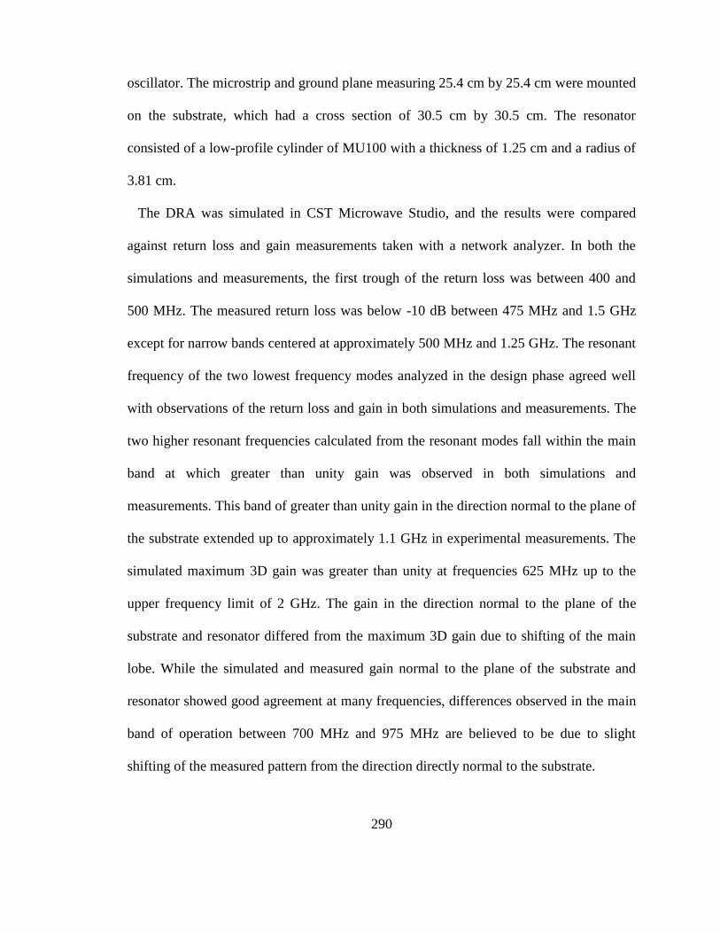
290
oscillator. The microstrip and ground plane measuring 25.4 cm by 25.4 cm were mounted
on the substrate, which had a cross section of 30.5 cm by 30.5 cm. The resonator
consisted of a low-profile cylinder of MU100 with a thickness of 1.25 cm and a radius of
3.81 cm.
The DRA was simulated in CST Microwave Studio, and the results were compared
against return loss and gain measurements taken with a network analyzer. In both the
simulations and measurements, the first trough of the return loss was between 400 and
500 MHz. The measured return loss was below -10 dB between 475 MHz and 1.5 GHz
except for narrow bands centered at approximately 500 MHz and 1.25 GHz. The resonant
frequency of the two lowest frequency modes analyzed in the design phase agreed well
with observations of the return loss and gain in both simulations and measurements. The
two higher resonant frequencies calculated from the resonant modes fall within the main
band at which greater than unity gain was observed in both simulations and
measurements. This band of greater than unity gain in the direction normal to the plane of
the substrate extended up to approximately 1.1 GHz in experimental measurements. The
simulated maximum 3D gain was greater than unity at frequencies 625 MHz up to the
upper frequency limit of 2 GHz. The gain in the direction normal to the plane of the
substrate and resonator differed from the maximum 3D gain due to shifting of the main
lobe. While the simulated and measured gain normal to the plane of the substrate and
resonator showed good agreement at many frequencies, differences observed in the main
band of operation between 700 MHz and 975 MHz are believed to be due to slight
shifting of the measured pattern from the direction directly normal to the substrate.

291
In conclusion, the high power dielectric resonator antenna both demonstrated that
antenna dimensions could be reduced through the incorporation of the high dielectric
constant composites and the composites could be integrated into a high power antenna
design. Given the high dielectric constant of the resonator, the band of frequencies at
which greater than unity gain was observed was exceptionally wide. The radiation
efficiency was also not excessively low as the simulated values at 650 MHz and 825
MHz were 64.6% and 88.6%, respectively. The relatively wide bandwidth and high
radiation efficiency are contrary to conventional behavior of dielectric resonators
antennas incorporating resonators with high dielectric constants. However, the agreement
between the simulation and measured results and the consistency of the measured results
provides ample confidence that the observed performance is legitimate.
7.2.2 Future Work
Future work on the high power DRA should include investigations on the minimization
of the substrate size, scaling to lower frequency, and time-domain properties. The
dimensions of the substrate used in this work were largely required for the antenna’s
incorporation in the high power ring-down oscillator. The added capacitance of a long
microstrip feed increased the energy stored in the oscillator’s high voltage section.
However, the microstrip can be much shorter while still properly exciting the resonator
modes and maintaining much of the present antenna’s performance characteristics.
Preliminary measurements of the return loss have confirmed that shorter microstrips can
provide very similar coupling. The limiting factor in the minimization of the substrate
size may be the ground plane. As the ground plane size is reduced, the approximation of

292
an infinite ground plane is invalidated, resulting in changes to the farfield gain pattern
and other critical parameters. With an adequately sized ground plane for the resonator
and microstrip sizes, the relative ease with which the DRA can be experimentally tuned
will allow the minimization of the microstrip length and ground plane dimensions to be
identified through experimental trial with smaller substrates.
Scaling to lower frequency operation can be achieved with larger resonators, utilization
of high dielectric constant materials, or a combination of these approaches. Since the
resonant frequencies calculated for dielectric resonators are inversely proportional to the
square root of the permittivity of the resonator, there is a case of diminishing returns as
the dielectric constant is increased. This situation is one reason why there was relatively
little advantage to implementing MU550 as the resonator in this work instead of MU100.
Therefore, with a material like MU100 already in use, it may be more practical to
increase the dimensions of the resonator to scale to lower frequency. To achieve very low
frequencies of operation within volume or weight constraints, innovations in the
geometry of the resonator could be made to lower the resonant frequency without
necessitating impractically large resonators.
If future work on the high power DRA is directed towards high peak power
applications as studied in this work, further investigation on the time-domain behavior of
the antenna is needed. The antenna has the potential to reflect a significant amount of
power back to the source. This does not present a problem when the antenna is integrated
with a ring-down oscillator. However, some high power sources could be damaged or
have their operation degraded by energy reflected from the antenna. Further investigation
into the time-domain behavior of the antenna will enable better prediction of the transient

293
fields radiated by the antenna based on the signal applied to the antenna. From a more
complete study of the time-domain behavior of the antenna, modifications to the antenna
and selection of the high power source can be better informed to enhance transient
radiation of high peak power fields.
7.3 High Power Antenna Driver
7.3.1 Summary
A high power antenna driver was designed to drive an antenna with a damped
sinusoidal waveform incorporating high frequency signals. The system was based on a
concept of an explosive generator as a source driving an inductive energy storage system.
The inductive energy storage system pulse charges a high voltage oscillator and the high
power antenna. When the oscillator and antenna are switched to ground through a self-
breaking spark gap switch, a series of damped oscillations is present on the antenna. High
frequency content is superimposed on the main damped sinusoid due to reflections
intentionally created on the oscillator through impedance mismatches.
Since the high power antenna driver is intended for high peak power antenna
characterization, the driver is based on a simulator of an FCG rather than an actual
explosive generator. The FCG simulator was driven by a CLC-network to provide a
rising input voltage as a function of time. The rising voltage signal increases the rate at
which the current output increases in time. Experiments with the FCG simulator
confirmed that not only is the first derivative of the current output positive, but the
second derivative of the current output is also positive, indicating that the FCG simulator
produces an output more similar to actual FCGs than previous simulators.

294
The inductive energy storage system consisted of a solenoid inductor and an exploding
wire fuse. Upon vaporization of the fuse wires, the energy stored in the solenoid is
diverted to charge the high voltage oscillator and antenna structure to high voltage. The
high voltage oscillator consisted of coaxial transmission lines with an electrical length of
approximately 0.5 ns each. The antenna was driven from a connection point between the
transmission line sections. The mismatched impedance due to the addition of the DRA,
which also contains a transmission line, resulted in multiple reflections that produce a
high frequency signal on top of the high voltage damped sinusoid.
The high power antenna driver was tested in an RF-shielded enclosure due to the
potentially high radiated electric fields. The antenna cannot be characterized in this type
of enclosure or in the same vicinity as the pulsed power source. Despite the limitations in
characterizing the antenna under these conditions, the basic operation of the high power
antenna driver was demonstrated. Suggestions on how the high power antenna driver can
be transitioned to an environment in which the antenna can be effectively characterized at
high power are given in the next subsection.
In conclusion, the high power antenna driver has been shown to be feasible for
generating a high power damped sinusoid. However, the effectiveness at applying this
type of driver to antennas operating above a few hundred MHz is low. While high
frequency signal content in the operating range of the antenna can be generated as a part
of the damped sinusoidal signal, the power level of the high frequency signal content is
small in comparison to the main components of the signal. Therefore, this type of high
power antenna driver is best suited for high power antennas in the VHF band, and
alternatives are necessary for antennas in the UHF band.

295
One potential alternative high power source is a basic high voltage pulser with a fast
risetime. The pulser could take the form of a Marx bank, or a simple source such as the
PA-80 trigger generator used in dielectric strength testing could be applied with a
peaking switch to decrease the risetime. The fast risetime of a high voltage pulse contains
high frequency signal content that could be radiated by an antenna. This concept is
applied to impulse radiating antennas in which an antenna radiates the derivative of the
applied voltage waveform as an impulse of the electric field. The risetime of the voltage
signal can be tuned to ensure the frequency content of the signal includes components in
the operational bandwidth of the antenna. The peak magnitude of the voltage pulse could
also be controlled to drive the antenna at specified peak power levels. This type of system
also enables repetitive testing that is not possible with the single-shot antenna driver
based on an inductive energy storage system.
7.3.2 Future Work
The antenna driver based on the ring-down oscillator is best suited for antennas in the
VHF band. Thus a path forward is needed on how the system could be transitioned to
permit actual antenna characterization in the VHF band. The obvious requirement to
allow the antennas to be characterized at high power is that the antenna must be tested in
an anechoic chamber or outdoor test range where the effects of the radiated fields from
the pulsed power system driving the antenna can be minimized. Ideally, the antenna and
field measurement devices would be completely isolated from the pulsed power system.
The current system could be adapted to enable this isolation if a high voltage
transmission line rated to a peak voltage of at least 200 kV were fed into an anechoic

296
chamber. The high power oscillator would likely need to be integrated directly with the
antenna under test within the anechoic chamber to effectively drive it at high frequency.
The length of the high voltage transmission line feeding into the anechoic chamber would
not negatively affect the performance of the high power oscillator and antenna if the
resistor in series with the transmission lines of the high power oscillator were included
inside the anechoic chamber at the connection to the high power oscillator.
In the experiments described in the previous chapter, the peak charging voltage of the
high power oscillator was below the maximum levels possible with the system. To
increase the peak voltage to above 225 kV, the value of the resistor in series with the
transmission lines of the high power oscillator should be lowered from 1.4 kΩ to a value
of around 700 Ω. To increase the peak voltage further beyond that simulated in section
6.4, the charging voltage of capacitor bank C1 should be increased above 40 kV, and the
number of fuse wires should be increased to allow a higher peak current in the inductive
energy store before the fuse opens the circuit.
Future work on high power antenna drivers should also further develop the system
based on a fast rise time pulse. While many types of pulse generators could be adapted to
serve as a high power antenna driver of this kind, most will require a peaking switch to
decrease the rise time of the pulse’s leading edge. Preliminary research on an antenna
driver of this type was accomplished in this work by using the PA-80 pulse generator
with a peaking switch. Future work in this area must be concentrated on lowering the
inductance of the peaking switch and improving the switch’s connection to the antenna
feed. In addition to the development of the peaking switch, the time-domain response of

297
the antennas under test must be further investigated to optimize the antennas for a fast
rise time step input.

298
VITA
Kevin O’Connor earned the degrees of Master of Science in Electrical
Engineering and PhD in Electrical and Computer Engineering from the University of
Missouri. His research has focused on the cross-disciplinary fields of pulsed power and
materials science. In his masters-level research, Kevin O’Connor investigated a power
conditioning and compact RF system for use with flux compression generators. In the
course of this research, he focused on the development of compact pulse transformers,
exploding wire fuses, a high voltage capacitive-discharge RF generator, and a non-
destructive test bed for the simulation of flux compression generators. His PhD-level
research has concentrated on the development of high dielectric constant composite
materials for high power applications and the design and testing of a compact high power
dielectric resonator antenna.
Kevin O’Connor completed an internship with Sandia National Laboratories and
KTech Corp. of Albuquerque, NM in 2007. He was a fellow with the National Physical
Science Consortium through the sponsorship of Sandia National Laboratories from 2008
to 2011. He was a finalist for the student paper of the year award from the IEEE Nuclear
and Plasma Sciences Society at the 2011 IEEE International Pulsed Power Conference,
and he was awarded a Tom R. Burkes Outstanding Graduate Student Award at the 2012
IEEE International Power Modulator and High Voltage Conference. While completing
his PhD studies, he co-founded NanoElectromagnetics LLC of Columbia, MO to
commercialize high dielectric constant composite materials for compact antenna and high
energy density storage applications.