the following article appeared in journal of applied ... · instructions for use title mechanism of...
TRANSCRIPT

Instructions for use
Title Mechanism of yellow luminescence in GaN at room temperature
Author(s) Matys, M.; Adamowicz, B.
Citation Journal of Applied Physics, 121(6): 65104
Issue Date 2017-02-14
Doc URL http://hdl.handle.net/2115/68307
Rights The following article appeared in Journal of Applied Physics 121, 065104 (2017) and may be found athttp://aip.scitation.org/doi/10.1063/1.4975116.
Type article
File Information 1%2E4975116.pdf
Hokkaido University Collection of Scholarly and Academic Papers : HUSCAP

Mechanism of yellow luminescence in GaN at room temperatureM. Matys and B. Adamowicz
Citation: Journal of Applied Physics 121, 065104 (2017); doi: 10.1063/1.4975116View online: http://dx.doi.org/10.1063/1.4975116View Table of Contents: http://aip.scitation.org/toc/jap/121/6Published by the American Institute of Physics
Articles you may be interested in Formation mechanism of gold-based and gold-free ohmic contacts to AlGaN/GaN heterostructure field effecttransistorsJournal of Applied Physics 121, 065301065301 (2017); 10.1063/1.4975473
On the origin of interface states at oxide/III-nitride heterojunction interfacesJournal of Applied Physics 120, 225305225305 (2016); 10.1063/1.4971409
Photo-Hall-effect study of excitation and recombination in Fe-doped GaNJournal of Applied Physics 121, 065702065702 (2017); 10.1063/1.4975622
Au-free ohmic Ti/Al/TiN contacts to UID n-GaN fabricated by sputter depositionJournal of Applied Physics 121, 065703065703 (2017); 10.1063/1.4975485
Three-dimensional cathodoluminescence characterization of a semipolar GaInN based LED sampleJournal of Applied Physics 121, 075702075702 (2017); 10.1063/1.4976204
Self-organized patterns of fullerene on molecular nanotemplateJournal of Applied Physics 121, 054305054305 (2017); 10.1063/1.4975199

Mechanism of yellow luminescence in GaN at room temperature
M. Matys1,2,a) and B. Adamowicz2
1Research Center for Integrated Quantum Electronics, Hokkaido University, Kita-13 Nishi-8,Kita-ku 060-8628 Sapporo, Japan2Surface Physics and Nanostructures Department, Institute of Physics - CSE, Silesian University of Technology,Konarskiego 22B, 44-100 Gliwice, Poland
(Received 16 October 2016; accepted 17 January 2017; published online 10 February 2017)
We investigated the excitation intensity (U) dependent photoluminescence (PL), at room temperature
(RT), from GaN-based metal-insulator-semiconductor structures under gate bias (VG) from accumula-
tion to deep depletion resulting in variations of the space charge region width. We found that depend-
ing on VG, different U-dependencies of the YL band energy position (blueshift or redshift), shape
(band enlargement or narrowing) and intensity (signal saturation) can be obtained. In order to explain
such an unusual YL behavior, we developed a phenomenological PL model, which is based on the
solution of the three-dimensional Poisson’s equation, current continuity equations and rate equations,
and which takes into account the grain structure of GaN layers and the contribution of interface
regions into recombination processes. Our model reproduced well the experimental U-dependencies
of the YL band intensity. It also predicts that YL arises from the donor-acceptor pair (DAP) recombi-
nation in very limited areas (width of several nanometers) inside the depletion regions related to
grain/grain interfaces and external crystal surfaces. On this basis, we showed that VG-controlled U-
dependencies of the YL peak position and shape, can be well explained if we assume that YL is due
to DAP-type transitions, in which the final state consists of the Coulomb interaction and strong inter-
action between the dipole moment of ionized DAP and the depletion region electric field. This
recombination mechanism can play a significant role at RT, but should be negligible at low tempera-
tures, where one can expect the significant reduction of interface barriers under illumination.
Published by AIP Publishing. [http://dx.doi.org/10.1063/1.4975116]
I. INTRODUCTION
Photoluminescence (PL) was widely used as a key tool
to study the material properties of wide band gap semicon-
ductors (WBGS) like GaN, which plays a crucial role in
technology of light-emitting1 and high-power electronic
devices.2 The most controversial and often observed in PL
spectrum of GaN is the broad yellow luminescence (YL)
band, whose source still remains a puzzle.3–11 Generally, YL
in GaN is interpreted in terms of two fundamental recombi-
nation mechanisms: (i) donor-acceptor pair (DAP) transi-
tions, in which the final state (ionized pair) is determined by
the Coulomb interaction12–15 and (ii) free-to-bound (eA)
type transitions.3,16,17
However, in this work, we demonstrate that (1) YL in
GaN at room temperature (RT) can arise as a result of DAP-
type transitions, in which the final state is determined by not
only the Coulomb interaction but predominately by the strong
interaction between the dipole moment of the ionized DAP
and the electric field in the depletion region, and (2) broaden-
ing of the YL band at RT can be due to the angular distribu-
tion of dipole moments with respect to the electric field. In
this purpose, we carried out the systematic measurements of
the excitation intensity (U) dependencies of PL spectra from
GaN-based metal-insulator-semiconductor (MIS) structures
at the different gate bias (VG) controlling the space charge
region (SCR) width (WSCR). To the best of our knowledge, no
similar studies had been conducted for GaN. We observed
that depending on VG, different U-dependencies of the YL
band energy position (blueshift or redshift), shape (band
enlargement or narrowing) and intensity (signal saturation)
can be obtained. In order to explain such an unusual YL
behavior, we developed a phenomenological model, which is
based on the solution of the three-dimensional (3D) Poisson’s
equation, current continuity equations and rate equations, and
which takes into account the grain structure of a GaN layer
and the contribution of interface regions into the recombina-
tion processes.
II. EXPERIMENT
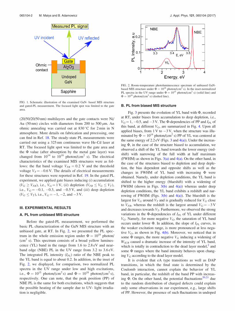
The schematic illustration of the investigated GaN-
based MIS structure and gated-PL measurement is shown in
Fig. 1. The MIS structures were fabricated using intention-
ally undoped n-GaN films with a free electron concentration
Nd ¼ 1017 cm�3 and thickness of 2.5 lm grown by means of
metalorganic chemical vapor deposition (MOCVD) tech-
nique on a sapphire substrate. The GaN layers were passiv-
ated with Al2O3 atomic layer deposition (ALD) insulating
film (thickness of 20 nm). In the passivation process, a two-
step approach was applied, namely, at first, the coverage
with a 10 nm thick SiN protection film deposited by electron
cyclotron resonance chemical vapor deposition (ECR CVD)
to avoid GaN damages during ohmic contact annealing, fol-
lowed by removal of this film, and subsequent deposition of
Al2O3. The ohmic contacts were ring-shaped Ti/Al/Ti/Aua)[email protected]
0021-8979/2017/121(6)/065104/12/$30.00 Published by AIP Publishing.121, 065104-1
JOURNAL OF APPLIED PHYSICS 121, 065104 (2017)
(20/50/20/50 nm) multilayers and the gate contacts were Ni/
Au (50 nm) circles with diameters from 200 to 500 lm. An
ohmic annealing was carried out at 830 �C for 2 min in N
atmosphere. More details on fabrication and processing, one
can find in Ref. 18. The steady-state PL measurements were
carried out using a 325 nm continuous wave He-Cd laser at
RT. The focused light spot was limited to the gate area and
the U value (after absorption by the metal gate layer) was
changed from 1014 to 1018 photon/(cm2 s). The electrical
characteristics of the examined MIS structures were as fol-
lows: the flat band voltage VFB ¼ 0:2 V and the threshold
voltage VT¼�0.6 V. The details of electrical measurements
for these structures were reported in Ref. 19. In the gated PL
experiment, we applied gate biases inducing (i) accumulation
(VG � VFB), i.e., VG¼ 1 V, (ii) depletion (VFB � VG � VT),
i.e., VG¼�0.1, �0.3, and �0.5 V, and (iii) deep depletion
(VG � VT), i.e., VG¼�1, �2, and �3 V.
III. EXPERIMENTAL RESULTS
A. PL from unbiased MIS structure
Before the gated-PL measurement, we performed the
basic PL characterization of the GaN MIS structure with an
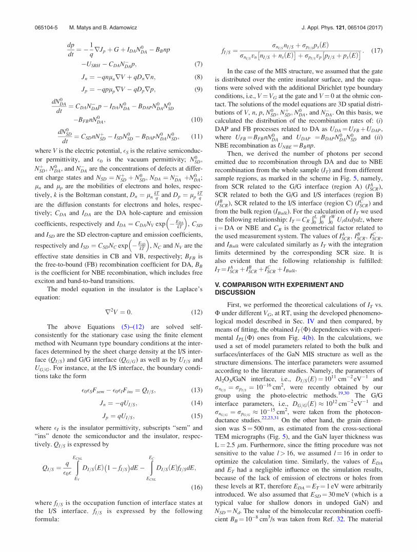
unbiased gate, at RT. In Fig. 2, we presented the PL spec-
trum in the whole emission region under U ¼ 1018 photon/
(cm2 s). This spectrum consists of a broad yellow lumines-
cence (YL) band in the range from 1.6 to 2.8 eV and near-
band edge (NBE) PL in the UV range from 3.2 to 3.6 eV.
The integrated PL intensity (IPL) ratio of the NBE peak to
the YL band is equal to about 0.2. In addition, in the inset of
Fig. 2, we displayed, for comparison, two normalized PL
spectra in the UV range under low and high excitations,
i.e., U ¼ 1015 photon/(cm2 s) and U ¼ 1018 photon/(cm2 s),
respectively. One can note, that the peak position (PP) of
NBE PL is the same for both excitations, which suggests that
the possible heating of the sample due to UV- light irradia-
tion is negligible.
B. PL from biased MIS structure
Fig. 3 presents the evolution of YL band with U, recorded
at RT, under biases from accumulation to deep depletion, i.e.,
VG¼ 1, �0.5, and �3 V. The U-dependencies of PP and IPL of
this band, at different VG, are summarized in Fig. 4. Upon all
applied biases, from 1 V to �3 V, when the structure was illu-
minated by U ¼ 1014 photon/(cm2 s) PP of YL was centered at
the same energy of 2.2 eV (Figs. 3 and 4(a)). Under the increas-
ing U, in the case of the structure biased to accumulation, we
observed a shift of the YL band towards the lower energy (red-
shift) with narrowing of the full width at half maximum
(FWHM) as shown in Figs. 3(a) and 4(a). On the other hand, in
the case of the structures biased to depletion and deep deple-
tion, the bias dependent and opposite shifts as well as the
changes in FWHM of YL band with increasing U were
obtained. Namely, under depletion conditions, the YL band is
shifted to the higher energy (blueshift) with a widening of
FWHM (shown in Figs. 3(b) and 4(a)) whereas under deep
depletion conditions, the YL band exhibits a redshift and nar-
rowing of FWHM (Figs. 3(b) and 4(a)). The blueshift is the
largest for VG around VT and is gradually reduced for VG close
to VFB, whereas the redshift is the largest around VG¼�3 V
and decreases towards VT. Furthermore, we observed the strong
variations in the U-dependencies of IPL of YL under different
VG. Namely, for more negative VG, the saturation of YL band
occurs under lower U. In addition, the slope of IPL curves, in
the weaker excitation range, is more pronounced at less nega-
tive VG, as shown in Fig. 4(b). Moreover, we noticed that in
some U ranges, the more negative VG inducing a widening of
WSCR caused a dramatic increase of the intensity of YL band,
which is totally in contradiction to the dead layer model,2 and
some U ranges where the band intensity behaves upon chang-
ing VG according to the dead layer model.
It is evident that eA type transitions as well as DAP
transitions, in which the final state is determined by the
Coulomb interaction, cannot explain the behavior of YL
band, in particular, the redshift of the band PP with increas-
ing U. On the other hand, the potential fluctuations20,21 due
to the random distribution of charged defects could explain
only some observations in our experiment, e.g., large shifts
of PP. However, the presence of such fluctuations in undoped
FIG. 1. Schematic illustration of the examined GaN- based MIS structure
and gated-PL measurement. The focused light spot was limited to the gate
area.
FIG. 2. Room-temperature photoluminescence spectrum of unbiased GaN-
based MIS structure under U ¼ 1018 photon/(cm2 s). In the inset-normalized
PL spectra in the UV range under U ¼ 1015 photon/(cm2 s) (solid line) and
U ¼ 1018 photon/(cm2 s) (dashed line).
065104-2 M. Matys and B. Adamowicz J. Appl. Phys. 121, 065104 (2017)

n-GaN samples is of low probability. Furthermore, we
excluded the surface related YL mechanisms22–25 because of
an U-shaped continuum of non-radiative interface states exist-
ing at the Al2O3/GaN interface.19 Moreover, it is evident that
the obtained dependencies of IPL cannot be explained by mod-
els based on the “dead layer” assumption (lack of radiative
recombination in the depletion region). Therefore, an entirely
new mechanism of YL is needed to explain our results.
IV. MODEL
In order to clarify the mechanism of YL, we proposed
the following model schematically illustrated in Fig. 5.
Let us consider a passivated semiconductor layer with the
columnar grain structure, which is often observed in cross-
sectional transmission electron microscopy (TEM) micro-
graphs26 of GaN like in the image displayed in Fig. 5. The
considered layer thickness is L and the length is equal to width
W ¼ l0:5S, where l is the number of grains, and S is the grain
dimension. Then, let us assume that the layer contains: (i)shallow donors (SD) with the concentration NSD and binding
energy ESD, (ii) deep acceptors (DA) with the concentration
NDA and binding energy EDA, (iii) non-radiative centers with
the binding energy ET and (iv) interface states at the insulator/
semiconductor (I/S) interfaces with the density distribution
DI=SðEÞ and at the grain-grain (G/G) interfaces with the den-
sity DG=GðEÞ. Let us also assume that the interface states at
I/S and G/G interfaces consist of both donor-like states distrib-
uted in the lower part of the band gap and acceptor-like ones
in the upper part, which are separated by the charge neutrality
level ECNL (for GaN, ECNL ¼ EC–1.1 eV,19 where EC is the
bottom of the conduction band (CB)).
In the dark, the negatively charged acceptor-like inter-
face states induce the band bending at I/S and G/G interfa-
ces, as shown in the insets in Fig. 5. Upon the UV
illumination, the excess carriers are generated at a rate G
exponentially decayed from the I/S interface according to
the Lambert-Beer law, i.e., GðxÞ ¼ Gð0Þ expð�aa � x), where
G(0) is the generation rate at the I/S interface, aa¼ 1:2� 105
cm�1 is the absorption coefficient for GaN at 325 nm, and x
is the distance from the I/S interface. The excited carriers
become separated in the depletion layer, i.e., electrons are
FIG. 3. Evolution of the normalized PL spectrum from a GaN based MIS
structure with U increasing from 1014 to 1018 photon/(cm2 s) with a step of
one order of magnitude, at RT and under VG¼ 1 V (accumulation) (a),
VG¼�0.5 V (depletion) (b), and VG¼�3 V (c) (deep depletion).
FIG. 4. PP (a) and IPL (b) of the YL band from GaN based MIS structure as
a function of U at RT under different VG. Dashed lines were calculated using
Eq. (31). Solid lines are from a numerical solution of Eqs. (5)–(12) with the
fitting parameters from Table I.
065104-3 M. Matys and B. Adamowicz J. Appl. Phys. 121, 065104 (2017)

repelled into the bulk whereas holes are attracted towards the
interface (insets in Fig. 5). On the other hand, some holes are
captured by donor-like interface states and cause the reduc-
tion of the negative interface charge. Both these processes
result in the lowering of the interface band bending.
Furthermore, the excess carriers recombine non-radiatively
through the interface states at a rate UI=S and UG=G at I/S
and G/G interfaces, respectively, as presented in Fig. 5.
According to the Shockley-Read-Hall (SRH) statistics,27
UI=S is expressed by the following formula:
UI=S ¼ðEC
EV
rnI=SrpI=S
vnvp nI=SpI=Sð ÞDI=S Eð Þ dE
rnI=Svn nI=S þ ns Eð Þ� �
þ rpI=Svp pI=S þ ps Eð Þ� � ; (1)
where EV is the top of the valence band (VB); rnI=Sand rpI=S
are the cross sections for capturing electrons and holes,
respectively, by interface states at the I/S interface; vn and vp
are the thermal velocities of electrons and of holes, respec-
tively; and nI=S and pI=S are the concentrations of electrons
and holes, respectively, at the I/S interface; nI=S and pI=S
are the concentrations of electrons and holes at the I/S inter-
face, respectively, nsðEÞ ¼ NC exp½ðE� ECÞ=ðkTÞ� and psðEÞ¼ NV exp½ðEV � EÞ=ðkTÞ�. A similar relationship involving
the cross sections for electron (rnG=G) and hole capturing
(rpG=G), respectively and DG=GðEÞ, is valid for UG=G.
The carriers can also recombine radiatively through free
excitons and band-to-band transitions giving rise to the NBE
PL via defects as well as non-radiatively through defects by
a SRH mechanism27 with a rate USRH given by the formula
USRH ¼np
sn nþ n1 ETð Þ½ � þ sp pþ p1 ETð Þ½ � ; (2)
where sn and sp are the lifetimes of electrons and holes,
respectively; n and p are the electron and hole concentra-
tions, respectively; n1ðETÞ ¼ NC exp½ðET � ECÞ=ðkTÞ� and
p1ðETÞ ¼ NV exp½ðEV � ETÞ=ðkTÞ�.Moreover, let us assume that the radiative recombina-
tion via defects may occur by DAP-type transitions involv-
ing SD and DA and by eA type transitions involving CB and
DA. Furthermore, according to Colbow,28 let us assume that
the DAP recombination rate coefficient BDAP is dependent
on the depletion region electric field strength (F) and thus
expressed by28
BDAP ¼ ðBDAP0=R1Þj1� 8HR1j�0:5
expð�bÞ; (3)
where BDAP0is the proportionality constant, H ¼ qFad=
ð2ESD), R1 ¼ R=ad where R is the mean distance between
DAPs and ad is the effective Bohr radius, q> 0 is the ele-
mentary charge, and b is expressed by
b ¼ð2R1
g1
ð1� 2=g� 4=g2 � 4HgÞ0:5dg; (4)
where g1 is determined from a condition that the integrand in
Eq. (4) is equal to zero. One can note that in the region where
F¼ 0, BDAP is approximately equal to BDAP0expð�R1Þ,
which is the probability of recombination in the Thomas-
Hopfield model of DAP.29
The model equations are based on the 3D Poisson’s
equation, current continuity equations and rate equations
describing the change of the concentration of defects at dif-
ferent charge states. The model equations in a semiconductor
layer are as follows:
r2V ¼ � q
�0�Sp� nþ NþSD � N�DA
� �; (5)
dn
dt¼ 1
qrJn þ Gþ ISDN0
SD � BBnp
�USRH � CSDnNþSD � BFBnN0DA; (6)
FIG. 5. Schematic illustration of an UV illuminated passivated semiconduc-
tor layer with the columnar grain structure, according to the cross-sectional
TEM image of a GaN film in the studied MIS structure. In the insets - energy
band diagrams of near I/S and G/G interface regions with UI=S; DI=SðEÞ and
UG=G; DG=GðEÞ, respectively, as well as with marked drift, generation (G),
and recombination (R) processes.
TABLE I. The values of fitted parameters.
Parameter Value Unit
NDA 8� 1015 cm�3
CDA 10�7 cm3/s
CSD 10�7 cm3/s
BFB 10�10 cm3/s
BDAP010�10 cm3/s
s 10�7 s
R 10 nm
065104-4 M. Matys and B. Adamowicz J. Appl. Phys. 121, 065104 (2017)
dp
dt¼ � 1
qrJp þ Gþ IDAN0
DA � BBnp
�USRH � CDAN�DAp; (7)
Jn ¼ �qnlnrV þ qDnrn; (8)
Jp ¼ �qplprV � qDprp; (9)
dN0DA
dt¼ CDAN�DAp� IDAN0
DA � BDAPN0DAN0
SD
�BFBnN0DA; (10)
dN0SD
dt¼ CSDnNþSD � ISDN0
SD � BDAPN0DAN0
SD; (11)
where V is the electric potential, �S is the relative semiconduc-
tor permittivity, and �0 is the vacuum permittivity; N0SD;
NþSD; N0DA, and N�DA are the concentrations of defects at differ-
ent charge states and NSD ¼ NþSD þ N0SD; NDA ¼ N�DA þN0
DA;
ln and lp are the mobilities of electrons and holes, respec-
tively, k is the Boltzman constant, Dn ¼ lnkTq and Dp ¼ lp
kTq
are the diffusion constants for electrons and holes, respec-
tively; CDA and IDA are the DA hole-capture and emission
coefficients, respectively and IDA ¼ CDANV exp � EDA
kT
� �, CSD
and ISD are the SD electron-capture and emission coefficients,
respectively and ISD ¼ CSDNC exp � ESD
kT
� �, NC and NV are the
effective state densities in CB and VB, respectively; BFB is
the free-to-bound (FB) recombination coefficient for DA, BB
is the coefficient for NBE recombination, which includes free
exciton and band-to-band transitions.
The model equation in the insulator is the Laplace’s
equation:
r2V ¼ 0: (12)
The above Equations (5)–(12) are solved self-
consistently for the stationary case using the finite element
method with Neumann type boundary conditions at the inter-
faces determined by the sheet charge density at the I/S inter-
face (QI=S) and G/G interface (QG=G) as well as by UI=S and
UG=G. For instance, at the I/S interface, the boundary condi-
tions take the form
�0�SFsem � �0�IFins ¼ QI=S; (13)
Jn ¼ �qUI=S; (14)
Jp ¼ qUI=S; (15)
where �I is the insulator permittivity, subscripts “sem” and
“ins” denote the semiconductor and the insulator, respec-
tively. QI=S is expressed by
QI=S ¼q
�0�
ðECNL
EV
DI=S Eð Þ 1� fI=S
� �dE�
ðEC
ECNL
DI=S Eð ÞfI=SdE;
(16)
where fI=S is the occupation function of interface states at
the I/S interface. fI=S is expressed by the following
formula:
fI=S ¼rnI=S
nI=S þ rpI=Sps Eð Þ
rnI=Svn nI=S þ ns Eð Þ� �
þ rpI=Svp pI=S þ ps Eð Þ� � : (17)
In the case of the MIS structure, we assumed that the gate
is distributed over the entire insulator surface, and the equa-
tions were solved with the additional Dirichlet type boundary
conditions, i.e., V¼VG at the gate and V¼ 0 at the ohmic con-
tact. The solutions of the model equations are 3D spatial distri-
butions of V, n, p, N0SD; NþSD; N0
DA, and N�DA. On this basis, we
calculated the distribution of the recombination rates of: (i)DAP and FB processes related to DA as UDA¼UFBþUDAP,
where UFB¼BFBnN0DA and UDAP ¼BDAPN0
DAN0SD and (ii)
NBE recombination as UNBE¼BBnp.
Then, we derived the number of photons per second
emitted due to recombination through DA and due to NBE
recombination from the whole sample (IT) and from different
sample regions, as marked in the scheme in Fig. 5, namely,
from SCR related to the G/G interface (region A) (IASCR),
SCR related to both the G/G and I/S interfaces (region B)
(IBSCR), SCR related to the I/S interface (region C) (IC
SCR) and
from the bulk region (IBulk). For the calculation of IT we used
the following relationship: IT¼CR
Ð L0
ÐW0
ÐW0
Uidxdydz, where
i¼DA or NBE and CR is the geometrical factor related to
the used measurement system. The values of IASCR; IB
SCR; ICSCR,
and IBulk were calculated similarly as IT with the integration
limits determined by the corresponding SCR size. It is
also evident that the following relationship is fulfilled:
IT¼ IASCRþ IB
SCRþ ICSCRþ IBulk.
V. COMPARISON WITH EXPERIMENT ANDDISCUSSION
First, we performed the theoretical calculations of IT vs.
U under different VG, at RT, using the developed phenomeno-
logical model described in Sec. IV and then compared, by
means of fitting, the obtained ITðU) dependencies with experi-
mental IPLðU) ones from Fig. 4(b). In the calculations, we
used a set of model parameters related to both the bulk and
surfaces/interfaces of the GaN MIS structure as well as the
structure dimensions. The interface parameters were assumed
according to the literature studies. Namely, the parameters of
Al2O3/GaN interface, i.e., DI=SðEÞ¼ 1011 cm�2 eV�1 and
rnI=S¼ rpI=S
¼ 10�16 cm2, were recently obtained by our
group using the photo-electric methods.19,30 The G/G
interface parameters, i.e., DG=GðEÞ 1012 cm�2 eV�1 and
rnG=G¼ rpG=G
10�15 cm2, were taken from the photocon-
ductance studies.22,23,31 On the other hand, the grain dimen-
sion was S¼ 500 nm, as estimated from the cross-sectional
TEM micrographs (Fig. 5), and the GaN layer thickness was
L¼ 2.5 lm. Furthermore, since the fitting procedure was not
sensitive to the value l> 16, we assumed l¼ 16 in order to
optimize the calculation time. Similarly, the values of EDA
and ET had a negligible influence on the simulation results,
because of the lack of emission of electrons or holes from
these levels at RT, therefore EDA¼ET¼ 1 eV were arbitrarily
introduced. We also assumed that ESD¼ 30 meV (which is a
typical value for shallow donors in undoped GaN) and
NSD¼Nd. The value of the bimolecular recombination coeffi-
cient BB¼ 10�8 cm3/s was taken from Ref. 32. The material
065104-5 M. Matys and B. Adamowicz J. Appl. Phys. 121, 065104 (2017)

parameters of GaN were assumed according to Ref. 2, as fol-
lows: ln¼ 1200 cm 2/(V s), lp¼ 10 cm 2/(V s), �S¼ 10.35,
NC¼ 2.3� 1018 cm�3, and NV¼ 1.8� 1019 cm�3. The other
parameters, i.e., NDA, CDA, BFB, BDAP0, CSD, R, sp, and sn
were obtained from the fitting. Based on the recently reported
first-principle calculations33,34 and electrical measure-
ments,35,36 we were able to estimate fairly narrow ranges of
reasonable values, in which the fitted parameters could be
changed, i.e., NDA from 1014 to 1016 cm�3, CDA from 10�10 to
10�7 cm3/s, and CSD from 10�10 to 10�7 cm3/s, BFB from
10�13 to 10�10 cm3/s and BDAP0from 10�13 to 10�10 cm3/s. In
the calculations we assumed, for simplicity, that sp ¼ sn ¼ sis constant throughout the whole structure. The s value was
changed in a broad range from 10�4 s to 10�10 s. It should be
noted that the fitting can also be realized with sp 6¼ sn, how-
ever, the final results are close to those obtained in the case of
sp ¼ sn. The value of R should be larger than ad 2:3 nm,
because Eq. (3) is valid for R > ad. On the other hand, the
average donor�acceptor distance R is less than20 N�1=3t ,
where Nt is the total impurity concentration (a sum of donor
and acceptor concentrations). Since in our case (undoped n-
type GaN) the donor concentration is much higher than the
acceptor concentration, thus R should be less than N�1=3d 20
nm. As a result, R was changed from 3 nm to 20 nm.
The multi-parameter fitting of ITðU) curves to the mea-
sured IPLðU) dependencies was realized using a genetic algo-
rithm37 based method. The obtained values of fitted
parameters are displayed in Table I. As it is evident from
Fig. 4(b), the theoretical calculations of IT vs. U well repro-
duced the experimental U-dependencies of IPL under various
VG. However, one can note that the values of fitted parame-
ters BFB and BDAP0are different (by about two orders of mag-
nitude) than those reported in the literature, for example, by
Reshchikov et al.38–40 On the other hand, the values of CDA
and CSD of the order of 10�7 cm3/s are with a good agree-
ment with the data by Reshchikov et al.38–40 It should also
be noted that the determined NDA of the order of 1015 cm�3
is also consistent with the values reported by Reshchikov
et al.38,39 Furthermore, the obtained s¼ 10�7 s lies in the
range of the reported experimental values of s for GaN,41–43
from 10�9 s to 10�6 s. The difference in values of BFB and
BDAP0parameters can result from the fact that in our model,
we took into account the recombination in the depletion
regions. It should also be noted that we do not claim that the
values of parameters obtained from the fitting are unique or
very precise. They should be rather treated as illustration
that our phenomenological model with reasonable values can
predict an unusual behavior of PL from GaN both under VG
and U changing in wide ranges. In particular, the proposed
model predicted the VG-controlled saturation of YL intensity
and a drastic increase of the YL band intensity vs. more neg-
ative VG (leading to enlargement of the depletion layer
width), which is totally in contradiction with the dead layer
model.
From the comparison of the calculated dependencies IT
vs. U and experimental dependencies of IPL vs. U we found,
as shown in Fig. 4(b), that IT is approximately equal to: (i)
IASCR (because of the inequality
IBSCRþIC
SCRþIBulk
IT< 0:01), when
the structure is biased into accumulation, which would mean
that YL comes from the depletion regions related to the G/G
interfaces, as it is seen from the cross-section distributions of
UDA in Fig. 6(a), (ii) IBSCR (
IASCRþIC
SCRþIBulk
IT< 0:01), when the
structure is biased to depletion, which would mean that YL
originates from the depletion region parts common to G/G
and I/S interfaces, as shown in Fig. 6(b) and (iii) ICSCR
(IASCRþIB
SCRþIBulk
IT< 0:01), when the structure is biased to deep
depletion, which would mean that YL comes from the deple-
tion regions related to the I/S interface, as can be seen from
Fig. 6(c). Furthermore, the detailed analysis of UDA (Fig. 6)
showed that in all these cases YL would not originate from
FIG. 6. Calculated cross-section distributions of UDA under U¼ 1015 pho-
ton/(cm2 s) shown for two grains in the case of a structure biased to accumu-
lation (VG¼ 1 V) (a), depletion (VG¼�0.5 V) (b) and deep depletion
(VG¼�1 V) (c). Dashed lines mark the border of depletion regions. The
points A, B, and C indicate the locations where F was calculated vs. U, as
shown in Fig. 12(b).
065104-6 M. Matys and B. Adamowicz J. Appl. Phys. 121, 065104 (2017)

the entire depletion region but mainly from the very limited
narrow areas of these regions with a thickness of several
nanometers. It should be noted that the calculations also indi-
cate that in opposition to YL, NBE PL for all VG originates
mainly from the areas outside the depletion regions, as it is
seen from the cross-section distributions of UNBE in Fig. 7.
It is evident that the obtained result concerning YL is
totally opposed to the conventional wisdom that PL mostly
comes from areas outside the depletion regions. However,
this result can be well understood based on simple rate equa-
tions (Eqs. (10) and (11)) describing the change of the con-
centration of defects at different charge states. Namely, in
the stationary case, where dN0DA=dt ¼ 0 and dN0
SD=dt¼ 0,
and neglecting IDA in Eq. (10) (because of the lack of emis-
sion of holes from DA at RT), N0DA and N0
SD, from Eqs. (10)
and (11), can be expressed as follows:
N0SD ¼
CSDNSDn
ISD þ BDAPN0DA þ CSDn
; (18)
N0DA ¼
CDANDAp
CDApþ BFBnþ BDAPN0SD
: (19)
It can be easily shown that in the denominator in
Eq. (18), the following relationship is fulfilled at RT:
ISD BDAPN0DA þ CSDn. Namely, at this condition, for
ESD¼ 30 meV, expð� ESD
kT Þ 1=3 and thus ISD CSDNC=3.
Therefore, we have that NC 3ðBDAPN0DA=CSD þ nÞ.
Because CSD>BDAP and N0DA � Nd for n-type GaN, we
obtained that BDAPN0DA=CSD � Nd. Furthermore, it is evident
that n � Nd . Taking into account that in our case 3 Nd� 0.5
NC, we can write that 3ðBDAPN0DA=CSD þ nÞ � NC, which
ends the proof. On this basis, Eq. (18) takes the form
N0SD
CSDNSDn
ISD: (20)
In GaN, there exists high interface electric fields of the
order of magnitude of 105 V/cm. Such fields strongly attract
almost all photo-holes towards the interfaces and repel elec-
trons from the interfaces towards the bulk. In consequence, a
very high p and n gradients between the interface and the
bulk are induced, i.e., negligible/high p in the bulk/near the
interface, respectively and high/negligible n in the bulk/near
the interface, respectively, as shown in Fig. 8(a). Due to such
distributions of p and n, we can distinguish two regions (Fig.
8(a)), namely, region I, extending from the interface to the
point x1, in which n� p and region II, extending from x2 to
the bulk, in which n p. It should be noted that both x1 and
x2 points are located inside the depletion layer.
For region I, we can show that the following inequality
(see the denominator in Eq. (19)) is fully satisfied:
CDAp BFBnþ BDAPN0SD: (21)
Namely, the above inequality can be written as follows:
p BFBn=CDA þ BDAPN0SD=CDA: (22)
Because CDA>BFB, then BFBn=CDA < n. On the other
hand, using ISD CSDNC=3 and Eq. (20), we can write that
BDAPN0SD=CDA 3BDAPNSDn=ðCDANCÞ. From the fact that
CDA>BDAP and 3NSD < NC, it follows that 3BDAPNSDn=ðCDANCÞ < n. Therefore, we find that BFBn=CDA þ BDAP
N0SD=CDA < 2n. Because 2n� p (p is several orders larger
than n in region I) thus p BFBn=CDA þ BDAPN0SD=CDA. On
this basis, Eq. (19) in region I takes the simple form
N0DA NDA: (23)
This means that in region I, all DA are neutral as can be
seen in Fig. 8(a), which shows the calculated depth distribu-
tion of N0DA.
FIG. 7. Calculated cross-section distributions of UNBE under U¼ 1015 pho-
ton/(cm2 s) shown for two grains in the case of a structure biased to accumu-
lation (VG¼ 1 V) (a), depletion (VG¼�0.5 V) (b) and deep depletion
(VG¼�1 V) (c). Dashed lines mark the border of depletion regions.
065104-7 M. Matys and B. Adamowicz J. Appl. Phys. 121, 065104 (2017)

For region II (n p), we can prove that opposite
relationship p� BFBn=CDA þ BDAPN0SD=CDA is satisfied.
Namely, assuming that BFB � 10�12 cm3/s, BDAP
� 10�12 cm3/s, and CDA � 10�7 cm3/s, we obtain that
BFBn=CDA � 10�5n and BDAPN0SD=CDA � 10�5N0
SD. Taking
into account that in region II 10�5n p and 10�5N0SD p,
we find that BFBn=CDA þ BDAPN0SD=CDA 2p, which ends
the proof. Using this inequality and Eq. (20), Eq. (19) in
region II can be approximately written as follows:
N0DA
CDANDANC
BFBNC þ 3BDAPNSD
p
n: (24)
From the above equation, it follows that N0DA in region II
strongly decreases, as shown in Fig. 8(a), first due to the
rapid decrease of p and increase of n and subsequently due
to the constant n and decrease of p.
Taking into account Eqs. (20), (23), and (24), we can
express UDAP and UFB as follows.
In region I:
UFB ¼ BFBnN0DA BFBNDAn; (25)
UDAP ¼ BDAPN0DAN0
SD 3BDAPNDANSD
NCn: (26)
In region II:
UFB BFBCDANDANC
BFBNC þ 3BDAPNSDp; (27)
UDAP 3BDAPNSDCDANDA
NCBFB þ 3BDAPNSDp: (28)
The above Eqs. (25)–(28) indicate that UFB, UDAP, and
thus also UDA ¼ UDAP þ UFB increases, like n, from the inter-
face to the point x1, and strongly decreases, like p, from the
point x2 to the bulk, as shown in Fig. 8(b). From this it follows
that UFB, UDAP, and UDA should reach maximum in the deple-
tion layer in the range hx1; x2i, as in Fig. 8(b). In conse-
quence, almost all emissions related to DA will essentially
come from the near interface region. Furthermore, it should
be noted that the correlated increasing n and decreasing p in
the range from the interface up to the point x1 causes that
UNBE remains almost constant in this region, as shown in Fig.
8(b). On the other hand, the stronger increasing n than
decreasing p in the region located deeper gives that UNBE rises
up to the point beneath the depletion region, where it reaches
the maximum (Fig. 8(b)) As a result, the NBE emission
mostly comes from outside of the depletion regions.
From the performed analysis it follows that UFB, UDAP,
and UDA always reach a maximum inside the depletion region
independent of the BFB value (in the range 10�10 cm3/s
�BFB�10�12 cm3/s), BDAP (10�10 cm3/s �BDAP�10�12 cm3/s),
CDA (10�7 cm3/s �CDA�10�9 cm3/s), and CSD (10�7 cm3/s
�CSD�10�9 cm3/s) if the largely non-uniform distributions
of n and p exist, as in Fig. 8(a). In other words, UFB, UDAP,
and UDA exhibit the maximum value in the depletion layer
solely due to non-uniform p and n distributions induced by
high electric fields. The BFB, BDAP, CDA, and CSD parameters
can only influence the maximum intensity of the mentioned
rates. This means that exclusively high electric fields present
in GaN at RT would be responsible for the localization of
YL maximum in depletion regions. In addition, since BDAP is
enhanced by F [see Eqs. (3) and (4)], thus UDAPUFB in the
depletion regions, as illustrated in Fig. 8(b). This means that
the YL band would mainly be caused by DAP type
transitions.
Based on the above results, we can explain the obtained
relationship between IT and other components IASCR; IB
SCR, and
ICSCR. Namely, in the case of the structures biased into accu-
mulation, the photo-holes are collected near the G/G interface,
as shown in Fig. 9(a). As a result, the UDA maximum is also
located in the depletion region related to the G/G interface
(Fig. 6(a)) and thus IT IASCR (Fig. 4(b)). On the other hand,
when the structures are biased to depletion, the photo-holes
are gathered mainly close to the G/G and I/S interfaces (Fig.
9(b)). In consequence, the UDA maximum is located in the
part of the depletion region common to both these interfaces
(Fig. 6(b)) and thus IT IBSCR (Fig. 4(b)). Furthermore, under
deep depletion, the photo-holes are mostly collected near the
I/S interface (Fig. 9(c)) and thus the UDA maximum is placed
in the depletion region (Fig. 6(c)) related to this interface
resulting in IT ICSCR (Fig. 4(b)).
From the above results it follows that UDA is totally gov-
erned by the carrier distribution in the depletion region.
FIG. 8. Calculated in-depth distributions, from the I/S interface towards the
bulk, of: N0DA, p, n, N0
SD (a), UDA, UFB, UDAP, and UNBE (b). VG¼�1 V and
U¼ 1015 photon/(cm2 s).
065104-8 M. Matys and B. Adamowicz J. Appl. Phys. 121, 065104 (2017)

It would be a reason that for various VG, we obtained signifi-
cantly different U-dependencies of IPL for YL. For example,
VG¼�1 V induces UDA with the maximum located close to
the interface (case 1) whereas VG¼�3 V induces UDA with
the maximum located farther from the interface (case 2) as
shown in Fig. 10. This is because of the weaker attraction of
holes and weaker repelling electrons from the interface in
case 1 than in case 2. In case 1, the maximum value of UDA
saturates at higher U than in case 2, as shown in Fig. 10. As
a consequence, IPL of YL saturates at higher U in case 1 than
in case 2 (as illustrated in Fig. 4(b)). The different behavior
of UDA maximum vs. U can be well understood in terms of
the position of the hole quasi-Fermi level at the interface
(Efps). Namely, in case 1, Efps is at a larger distance from EV
than in case 2, as shown in Fig. 11(a) and therefore a rela-
tively higher U is necessary for Efps to reach EV. While Efps
approaches EV, p in the depletion region (Fig. 11(b)) and
consequently the UDA maximum saturates at a higher U in
case 1 compared to case 2.
Our model predicted that YL arises from the DAP
recombination in very limited areas inside the depletion
regions. On this basis, we concluded that both PP and
FWHM of YL can be dependent on F. This is because a pho-
ton emitted from DAP recombination under the field F has
the energy dependent on this field. It results from the interac-
tion between F and the dipole moment of the ionized DAP
created after recombination involving a neutral DAP.28 The
FIG. 9. Calculated cross-section distributions of p under U¼ 1015 photon/
(cm2 s) shown for two grains in the case of a structure biased into accumula-
tion (VG¼ 1 V) (a), depletion (VG¼�0.5 V) (b) and deep depletion
(VG¼�1 V) (c).
FIG. 10. Calculated in-depth distributions, from I/S interface towards the
bulk, of UDA as a function of U with a step of one order of magnitude. Solid
lines correspond to VG¼�1 V and dashed lines to VG¼�3 V.
FIG. 11. Calculated dependencies of Efps vs. U (a); in-depth distributions
from I/S interface of p as a function of U with a step of one order of magni-
tude (b). Solid lines are for VG¼�1 V and dashed lines for VG¼�3 V.
065104-9 M. Matys and B. Adamowicz J. Appl. Phys. 121, 065104 (2017)

emission energy (Eem) of DAP recombination in the deple-
tion region can be expressed by the relationship28
Eem ¼ Eg � EDA � ESD þ ECoul þ qFR cos a; (29)
where Eg is the energy band gap, ECoul is the Coulomb interac-
tion, and a is the angle between the DAP dipole moment and
F, and a takes values in the range28 �p=2 < a � p=2. Thus,
due to the dependence of Eem on a, the YL bandwidth should
be broadened by an amount DE approximately equal to28
DE 0:5qFR: (30)
Therefore, according to Eqs. (29) and (30), one can expect
that PP and FWHM of YL should exhibit a linear blueshift
and increasing FWHM with the rising F and, on the contrary,
a linear redshift and decreasing FWHM with the reduced F.
In order to prove the linear relationships between YL
parameters and F, we converted the measured PP dependen-
cies vs. U (Fig. 4(a)) into the dependencies vs. F (Fig.
12(a)). In the converting procedure we used the F values cal-
culated vs. U, at the points A, B, and C, as shown in Fig. 6.
The calculated dependencies F vs. U are shown in Fig.
12(b). From this analysis, we obtained the striking correla-
tion between PP and F, i.e., we found that all the data points
from the drastically differing dependencies of PP after con-
verting lie at a common straight line with a positive slope.
These results excellently confirm the predicted dependencies
of PP against F (see Eq. (29)) and also the quantitative analy-
sis of IPL (Fig. 4(b)) by the proposed model. Consequently,
we can express PP of YL as follows:
PP ¼ aFþ b; (31)
where a¼ 15 �10�10 q cm and b¼ 2.16 eV.
It should be noted that when F¼ 0 (lack of internal elec-
tric fields), PP of the YL band should be located at 2.16 eV.
By analogy to Eq. (29), the constant a in Eq. (31) should be
directly proportional to R. Thus, we can estimate R as fol-
lows: R ’ a=q ¼ 9 nm. It should be noted that this value is
in a good agreement with the value of R (Table I) indepen-
dently determined from the fitting of the IPL(U) dependen-
cies. This finding is an additional confirmation of the
quantitative analysis of IPL(U).
By substituting into Eq. (31), the calculated dependen-
cies of F vs. U (Fig. 12(b)) we reproduced very well the mea-
sured dependencies of PP (Fig. 4(a)). Thus, it is evident that
the changes of F are mainly responsible for the variety of
YL parameter evolution. Namely, in the case of the structure
biased to accumulation, YL is created in the depletion
regions of G/G interfaces (Fig. 6(a)), in which F decreases
vs. U, as shown in Fig. 12(b) (curve denoted A). As a result,
we observed the redshift of PP with a narrowing of FWHM
vs. U (Fig. 3(a)). On the contrary, in the case of the structure
biased to depletion, YL is generated in the part of the deple-
tion regions common for G/G and I/S interfaces (Fig. 6(b)),
in which F rises vs. U (Fig. 12(b), curve B). As a conse-
quence, we registered the blueshift of PP with a widening of
FWHM vs. U (Fig. 3(b)). However, in the case of the struc-
ture biased to deep depletion, YL is created in the depletion
region related to the I/S interface (Fig. 6(c)), in which Fdecreases vs. U (Fig. 12(b), curve C). As a result, we noted
the redshift of PP with a narrowing of FWHM vs. U (Fig.
3(c)). Furthermore, within the framework of Eq. (29), we can
explain why the variations of YL band shape occur mainly at
the band high-energy side, but not at its low-energy side
(Fig. 3). Namely, it is evident from Eq. (29) that the high-
energy part should be attributed to DAPs having dipole
moments approximately parallel to F (cos a 1) and, on the
contrary, the low-energy part of YL band should correspond
to DAPs with dipole moments approximately perpendicular
to F (cos a 0). Since the emission energy of DAPs with
cos a 0 is almost independent on F, therefore we did not
observe any visible changes at the lower energy side of the
YL band. On the other hand, because the emission energy of
DAPs with cos a 1 is dependent on F, we observed the
marked variations at the band high-energy side.
The above results indicate that YL may come from
DAP-type transitions, in which the final state comprises both
the Coulomb interaction and strong interaction of the dipole
moment with the electric field (see Eq. (29)). Furthermore,
the broadening of YL band can be due to the angular distri-
bution of dipole moments with respect to the electric field. It
should be noted that the dipole DAP-related recombination
mechanism of YL can play a significant role at RT when the
flat-band conditions cannot be easily achieved under contin-
uous illumination with typical HeCd laser fluxes, and thus
the band bending of about 0.3–0.6 eV may exist at GaN sur-
faces/interfaces. However, this recombination mechanism
can be negligible at low temperatures, because under a typi-
cal UV illumination of GaN, surface barriers mostly
FIG. 12. Dependencies of PP vs. F (a) obtained after converting measured
PP (U) dependencies from Fig. 4(a). The F values were obtained from the
calculated dependencies F(U) for different VG (b). The curves A (VG¼ 1 V),
B (�0.5 V), and C (�3 V) were calculated at points A, B, and C, respec-
tively, from Fig. 6. Dashed line is the best fit curve: PP ¼ aFþ b, where
a¼ 15� 10�10 cm/q and b¼ 2.16 eV.
065104-10 M. Matys and B. Adamowicz J. Appl. Phys. 121, 065104 (2017)

disappear due to the strong surface photovoltage effect.44
Instead, at low temperatures, YL should be well described in
terms of electron-phonon coupling, as it was recently shown
by Reshchikov et al.,11 who observed a zero-phonon line and
a fine structure of the YL band.
It is important to stress that the developed phenomeno-
logical model, which takes into account the influence of local
electric fields on DAP recombination can explain, in a coher-
ent manner, various behaviors of YL. These are, for exam-
ple, (i) sample dependent variations of PP and FWHM of
YL,8 (ii) different dependencies of PP and FWHM vs. U,
including small and negligible blueshifts of PP7,12 or large
blueshifts of PP,45,46 (iii) often observed unstable behavior
of YL with time under UV illumination,47–49 (iv) changes of
YL shape after different surface treatment50 and (v) rising of
YL intensity vs. increase of surface states density, which was
observed by Shalish et al.22,23 and assigned to the radiative
surface states responsible for YL and (vi) cathodolumines-
cence images registered by Ponce et al.26,51 and others52
showing that YL is mainly emitted from the near grain
boundary regions. It is evident that all the above effects can
be attributed, in accordance with our model, to the variations
of surface band bending, which are responsible for the
changes in dipole energy and carrier distribution in the
depletion regions. However, it should also be noted that we
do not claim that the previous explanations of the above
problems (i-vi) are incorrect but we would just like to show
that our model offers an alternative interpretation of these
issues.
VI. CONCLUSIONS
We investigated the U-dependent PL at different VG
from the GaN-based MIS structure at RT. We found that for
different VG, various U-dependencies of the YL band energy
position, FWHM and intensity can be obtained. In particular,
we revealed that depending on the applied VG, the YL band
exhibited a blueshift or a redshift with increasing U. In order
to explain these results, we developed the phenomenological
model, which is based on the solution of the Poisson’s equa-
tion, current continuity equations, and rate equations with
the boundary conditions determined by the interface field
strength and nonradiative recombination at semiconductor
surfaces and grain boundaries. Our model reproduced well
the experimental U-dependencies of YL band intensity. It
also, predicts that YL arises from the DAP recombination in
very limited areas (width of several nanometers) inside
depletion regions related to grain/grain interfaces and exter-
nal crystal surfaces. On this basis, we showed that VG-con-
trolled U–dependencies of YL peak position and FWHM,
can be well explained if we assume that YL is due to DAP-
type transitions, in which the final state consists of the
Coulomb interaction and strong interaction between the
dipole moment of ionized DAP and the depletion region
electric field. This recombination mechanism can play a sig-
nificant role at RT, but should be negligible at low tempera-
tures, where one can expect the reduction of interface
barriers under UV illumination due to the strong surface
photovoltage effect. Finally, we demonstrated that the
proposed phenomenological model, which takes into account
the influence of local electric fields on DAP recombination
can serve as a coherent explanation of various behaviors of
defect related PL.
ACKNOWLEDGMENTS
One of the authors, M.M., thanks the Research Center
for Integrated Quantum Electronics (RCIQE), Hokkaido
University, Sapporo, Japan for the postdoctoral fellowship
and the members of RCIQE for their kind assistance. M.M.
expresses gratitude to Professor Tamotsu Hashizume
(RCIQE) for his kind support and discussions, Professor
Yunichi Motohisa (RCIQE) for his help in PL experiment
and Dr. Zenji Yatabe (Kumamoto University) for TEM
images. The work was partially supported by the InTechFun
project (UDA-POIG.01.03.01.00-159/08-04) of EU
Structural Funds in Poland and the SAFEMOST project (14/
990/PNN16/0072) within the Visegrad Group (V4)-Japan
Joint Research Program on Advanced Materials.
1S. Nakamura and G. Fasol, The Blue Laser-Diode GaN Based LightEmitters and Lasers (Springer-Verlag, Berlin, 1997).
2H. Morkoc, Handbook on Nitride Semiconductors and Devices, GaN-Based Optical and Electronic Devices, Vol. 3 (Wiley, Weinheim, 2009).
3J. L. Lyons, A. Janotti, and C. G. Van de Walle, Appl. Phys. Lett. 97,
152108 (2010).4S. G. Christenson, W. Xie, Y. Y. Sun, and S. B. Zhang, J. Appl. Phys. 118,
135708 (2015).5D. Demchenko, I. Diallo, and M. A. Reshchikov, Phys. Rev. Lett. 110,
087404 (2013).6S. Ito, T. Nakagita, N. Sawaki, H. Ahn, M. Irie, T. Hikosaka, Y. Honda,
M. Yamaguchi, and H. Amano, Jpn. J. Appl. Phys. 53, 11RC02 (2014).7M. A. Reshchikov, D. O. Demchenko, A. Usikov, H. Helava, and Y.
Makarov, Phys. Rev. B 90, 235203 (2014).8M. A. Reshchikov and H. Morkoc, J. Appl. Phys. 97, 061301 (2005).9M. A. Reshchikov, A. Usikov, H. Helava, and Y. Makarov, Appl. Phys.
Lett. 104, 032103 (2014).10M. A. Reshchikov, J. Q. Xie, B. Hertog, and A. Osinsky, J. Appl. Phys.
103, 103514 (2008).11M. A. Reshchikov, J. D. McNamara, F. Zhang, M. Monavarian, A.
Usikov, H. Helava, Y. Makarov, and H. Morkoc, Phys. Rev. B 94, 035201
(2016).12T. Ogino and M. Aoki, Jpn. J. Appl. Phys., Part 1 19, 2395 (1980).13J. Neugebauer and C. G. Van de Walle, Appl. Phys. Lett. 69, 503 (1996).14J. S. Colton, P. Y. Yu, K. L. Teo, E. R. Weber, P. Perlin, I. Grzegory, and
K. Uchida, Appl. Phys. Lett. 75, 3273 (1999).15A. Sedhain, J. Li, J. Y. Lin, and H. X. Jiang, Appl. Phys. Lett. 96, 151902
(2010).16T. Suski, P. Perlin, H. Teisseyre, M. Leszczynsky, I. Grzegory, J. Jun, M.
Bockowski, S. Porowski, and T. D. Moustakas, Appl. Phys. Lett. 67, 2188
(1995).17H. M. Chen, Y. F. Chen, M. C. Lee, and M. S. Feng, Phys. Rev. B 56,
6942 (1997).18C. Mizue, Y. Hori, M. Miczek, and T. Hashizume, Jpn. J. Appl. Phys., Part
1 50, 021001 (2011).19M. Matys, B. Adamowicz, and T. Hashizume, Appl. Phys. Lett. 101,
231608 (2012).20B. I. Shklovskii and A. L. Efros, Electronic Properties of Doped
Semiconductors (Springer, Berlin, 1984).21A. P. Levanyuk and V. V. Osipov, Usp. Fiz. Nauk. 133, 427 (1981).22I. Shalish, L. Kronik, G. Segal, Y. Rosenwaks, Y. Shapira, U. Tisch, and J.
Salzman, Phys. Rev. B 59, 9748 (1999).23I. Shalish, L. Kronik, G. Segal, Y. Shapira, S. Zamir, B. Meyler, and J.
Salzman, Phys. Rev. B 61, 15573 (2000).24M. A. Reshchikov, P. Visconti, and H. Morkoc, Appl. Phys. Lett. 78, 177
(2001).25J. I. Izpura, Adv. Condens. Matter Phys. 2013, 597265 (2013).
065104-11 M. Matys and B. Adamowicz J. Appl. Phys. 121, 065104 (2017)

26F. A. Ponce and D. P. Bour, Nat. London 386, 351 (1997).27W. Shockley and W. T. Read, Phys. Rev. 87, 835 (1952).28K. Colbow, Phys. Rev. 139, A274 (1965).29D. G. Thomas, J. J. Hopfield, and W. M. Augustyniak, Phys. Rev. 140,
A202 (1965).30M. Matys, R. Stoklas, J. Kuzmik, B. Adamowicz, Z. Yatabe, and T.
Hashizume, J. Appl. Phys. 119, 205304 (2016).31N. Sarkar, S. Dhar, and S. Ghosh, J. Phys.: Condens. Matter 15, 7325
(2003).32F. Binet, J. Y. Duboz, E. Rosencher, F. Scholz, and V. Harle, Appl. Phys.
Lett. 69, 1202 (1996).33A. Alkauskas, Q. Yan, and C. G. Van de Walle, Phys. Rev. B 90, 075202
(2014).34J. L. Lyons, A. Alkauskas, A. Janotti, and C. G. Van de Walle, Phys.
Status Solidi B 252, 900 (2015).35P. Kamyczek, E. Placzek-Popko, V. Kolkovsky, S. Grzanka, and R.
Czernecki, J. Appl. Phys. 111, 113105 (2012).36D. Bisi, M. Meneghini, C. de Santi, A. Chini, M. Dammann, P. Brckner,
M. Mikulla, G. Meneghesso, and E. Zanoni, IEEE Trans. Electron Devices
60, 3166 (2013).37A. Domanowska, M. Miczek, R. Ucka, M. Matys, B. Adamowicz, J.
Zywicki, A. Taube, K. Korwin-Mikke, S. Gieratowska, and M. Sochacki,
Appl. Surf. Sci. 258, 8354 (2012).38M. A. Reshchikov and R. Y. Korotkov, Phys. Rev. B 64, 115205
(2001).39M. A. Reshchikov, Appl. Phys. Lett. 88, 202104 (2006).
40M. A. Reshchikov, A. J. Olsen, M. F. Bishop, and T. McMullen, Phys.
Rev. B 88, 075204 (2013).41Z. Z. Bandic, P. M. Bridger, E. C. Piquette, and T. C. McGill, Appl. Phys.
Lett. 72, 3166 (1998).42K. Kumakura, T. Makimoto, N. Kobayashi, T. Hashizume, T. Fukui, and
H. Hasegawa, Appl. Phys. Lett. 86, 052105 (2005).43M. Kato, H. Watanabe, M. Ichimura, and E. Arai, Mater. Res. Soc. Symp.
Proc. 831, 107 (2006).44L. Kronik and Y. Shapira, Surf. Sci. Rep. 37, 1 (1999).45M. A. Reshchikov, H. Morkoc, S. S. Park, and K. Y. Lee, Appl. Phys.
Lett. 78, 2882 (2001).46M. A. Reshchikov, H. Morkoc, S. S. Park, and K. Y. Lee, Appl. Phys.
Lett. 78, 3041 (2001).47M. A. Reshchikov, Y. T. Moon, and H. Morkoc, Phys. Status Solidi C 2,
2716 (2005).48S. A. Brown, R. J. Reeves, C. S. Haase, R. Cheung, C. Kirchner, and M.
Kamp, Appl. Phys. Lett. 75, 3285 (1999).49B. J. Ryan, M. O. Henry, E. McGlynn, and J. Fryar, Physica B 340–342,
452 (2003).50R. Cheung, R. J. Reeves, S. A. Brown, E. van der Drift, and M. Kamp,
J. Appl. Phys. 88, 7110 (2000).51F. A. Ponce, D. P. Bour, W. Gotz, and P. J. Wright, Appl. Phys. Lett. 68,
57 (1996).52L. J. Brillson, T. M. Levin, G. H. Jessen, A. P. Young, C. Tu, Y. Naoi, F.
A. Ponce, Y. Yang, G. J. Lapeyre, J. D. MacKenzie, and C. R. Abernathy,
Physica B 273–274, 70 (1999).
065104-12 M. Matys and B. Adamowicz J. Appl. Phys. 121, 065104 (2017)