the microarchitecture level - university of macedonia – contains address of potential next...
TRANSCRIPT

The Microarchitecture Level
Chapter 4
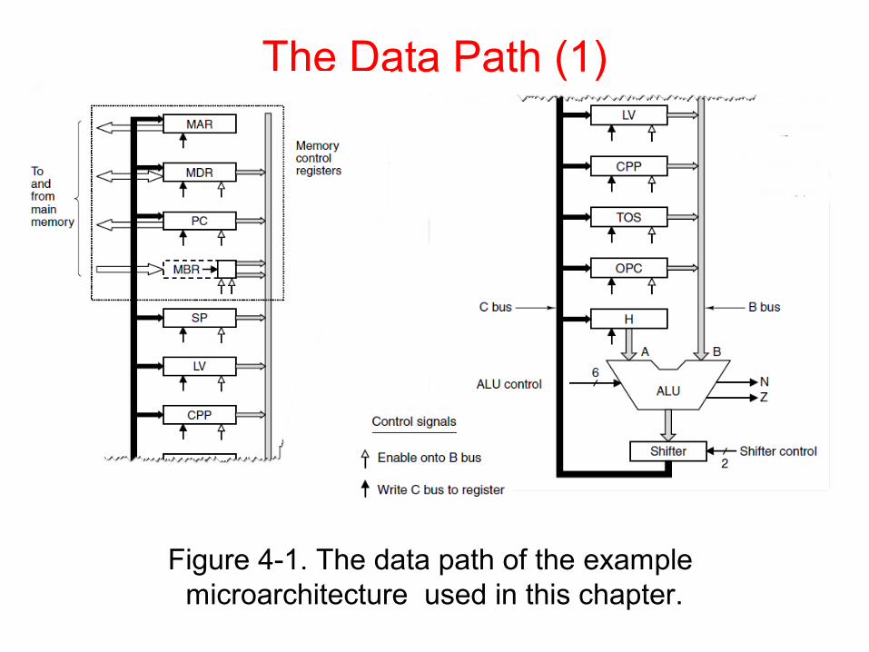
The Data Path (1)
Figure 4-1. The data path of the example microarchitecture used in this chapter.

The Data Path (2)
Figure 4-2. Useful combinations of ALU signals and the function performed.

Data Path Timing (1)
Figure 4-3. Timing diagram of one data path cycle.

Data Path Timing (2)
Activities of subcycles with subcycle length:
• The control signals are set up (Δw)• The registers are loaded onto the B bus (Δx)• The ALU and shifter operate (Δy)
• The results go along the C bus back to the registers (Δz)
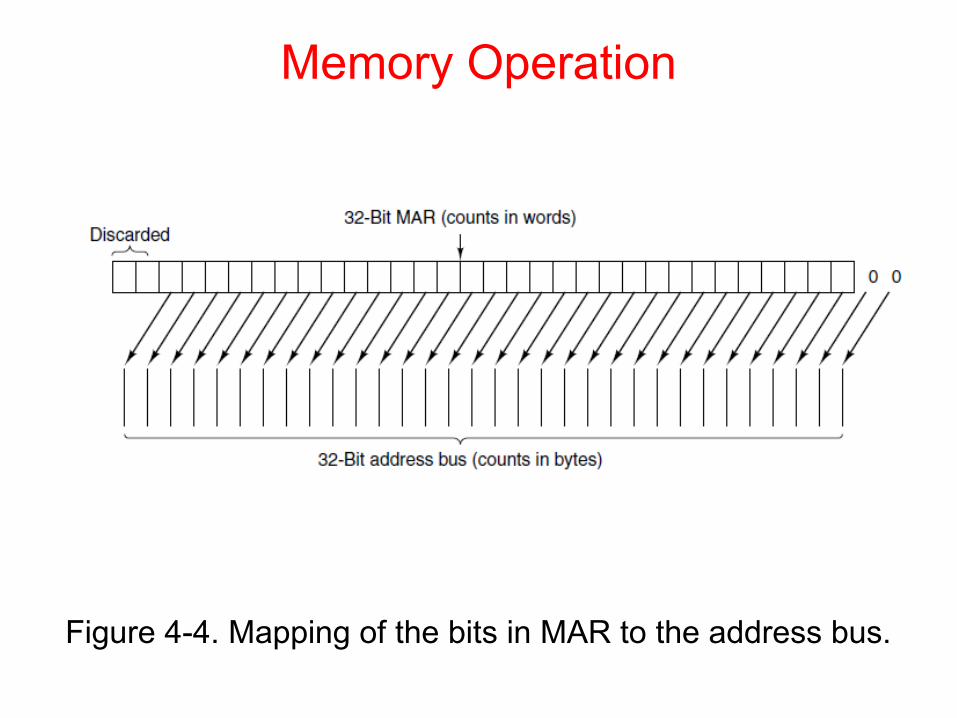
Memory Operation
Figure 4-4. Mapping of the bits in MAR to the address bus.

Microinstructions (1)
Functional Signal Groups:
9 Signals to control writing data from C bus into registers.
9 Signals to enable registers onto B bus for ALU input.
8 Signals to control ALU and shifter functions.
2 Signals to indicate memory read/write via MAR/MDR.
1 Signal to indicate memory fetch via PC/MBR.

Microinstructions (2)
Figure 4-5. The microinstruction format for the Mic-1.

Microinstructions (3)
Groups of signals:
Addr – Contains address of potential next microinstruction.
JAM – Determines how te next microinstruction selected.
ALU – ALU and shifter functions.
C – Selects which registers written from C bus.
Mem – Memory functions.
B – Selects B bus source; encoded as shown.

Microinstruction Control: The Mic-1 (1)
The sequencer must produce two kinds of information each cycle:
• The state of every control signal in the system• The address of the microinstruction that is to be executed next
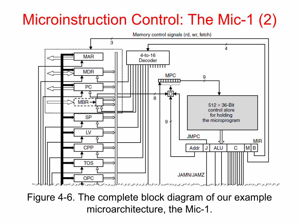
Microinstruction Control: The Mic-1 (2)
Figure 4-6. The complete block diagram of our example microarchitecture, the Mic-1.

Microinstruction Control: The Mic-1 (3)
Figure 4-6. The complete block diagram of our example microarchitecture, the Mic-1.

Microinstruction Control: The Mic-1 (4)
In all cases, MPC can take on only one of two possible values:
• The NEXT ADDRESS• The NEXT ADDRESS with the high-order bit ORed with 1

Microinstruction Control: The Mic-1 (5)
Figure 4-7. A microinstruction with JAMZ set to 1 has two potential successors.

Stacks (1)
Figure 4-8. Use of a stack for storing local variables. (a) While A is active. (b) After A calls B. (c) After B calls C. (d) After C and B
return and A calls D.

Stacks (2)
Figure 4-9. Use of an operand stack for doing
an arithmetic computation

The IJVM Memory Model (1)
Defined areas of memory
• The constant pool
• The Local variable frame
• The operand stack• The method area

The IJVM Memory Model (2)
Figure 4-10. The various parts of the IJVM memory.
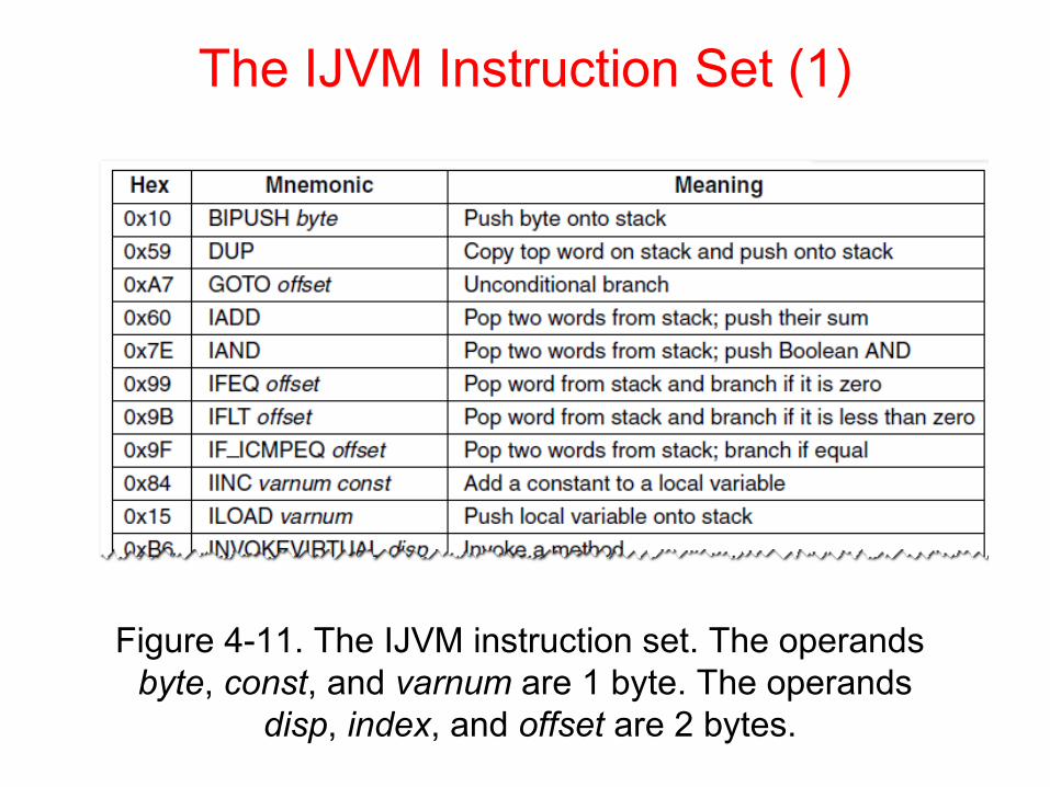
The IJVM Instruction Set (1)
Figure 4-11. The IJVM instruction set. The operands byte, const, and varnum are 1 byte. The operands
disp, index, and offset are 2 bytes.

The IJVM Instruction Set (2)
Figure 4-11. The IJVM instruction set. The operands byte, const, and varnum are 1 byte. The operands
disp, index, and offset are 2 bytes.

The IJVM Instruction Set (3)
Figure 4-12. (a) Memory before executing INVOKEVIRTUAL. (b) After executing it.

The IJVM Instruction Set (4)
Figure 4-13. (a) Memory before executing IRETURN. (b) After executing it.

Compiling Java to IJVM (1)
Figure 4-14. (a) A Java fragment. (b) The corresponding Java assembly language. (c) The IJVM program in hexadecimal.

Compiling Java to IJVM (2)
Figure 4-15. The stack after each instruction of Fig. 4-14(b).

Microinstructions and Notation
Figure 4-16. All permitted operations. Any of above operations may be extended by adding ‘‘<< 8’’ to them to shift result left by 1
byte. Example: common operation H = MBR << 8.
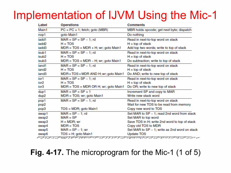
Implementation of IJVM Using the Mic-1
Fig. 4-17. The microprogram for the Mic-1 (1 of 5)

Implementation of IJVM Using the Mic-1
Fig. 4-17. The microprogram for the Mic-1 (2 of 5)

Implementation of IJVM Using the Mic-1
Fig. 4-17. The microprogram for the Mic-1 (3 of 5)

Implementation of IJVM Using the Mic-1
Fig. 4-17. The microprogram for the Mic-1 (4 of 5)
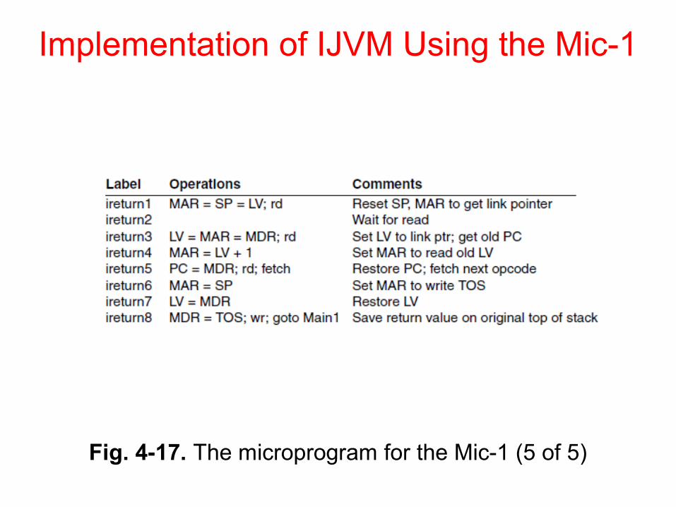
Implementation of IJVM Using the Mic-1
Fig. 4-17. The microprogram for the Mic-1 (5 of 5)

Implementation of IJVM Using the Mic-1 (2)
Figure 4-18. The BIPUSH instruction format

Implementation of IJVM Using the Mic-1 (3)
Figure 4-19. (a) ILOAD with a 1-byte index. (b) WIDE ILOAD with a 2-byte index.

Implementation of IJVM Using the Mic-1 (4)
Figure 4-20. The initial microinstruction sequence for ILOAD and WIDE ILOAD. The addresses are examples.
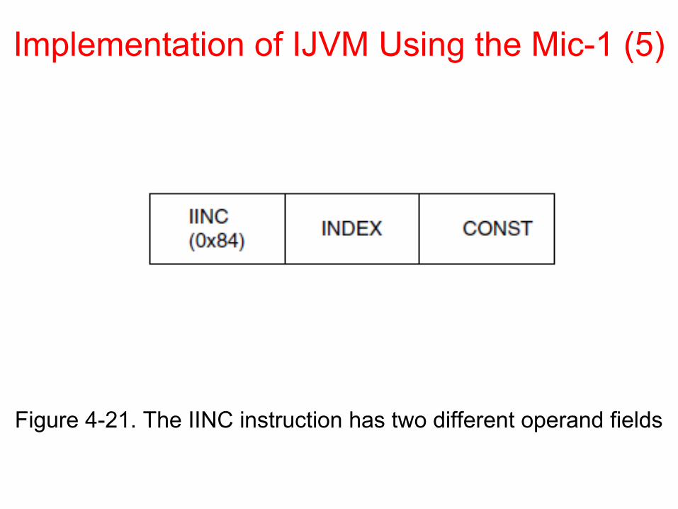
Implementation of IJVM Using the Mic-1 (5)
Figure 4-21. The IINC instruction has two different operand fields

Implementation of IJVM Using the Mic-1 (6)
Figure 4-22. The situation at the start of various microinstructions. (a) Main1. (b) goto1. (c) goto2. (d) goto3. (e) goto4.

Speed versus Cost
Basic approaches for increasing the speed of execution:
• Reduce # of clock cycles needed to execute an instruction• Simplify organization so that clock cycle can be shorter• Overlap execution of instructions

Merging Interpreter Loop with Microcode (1)
Figure 4-23. Original microprogram sequence for executing POP.
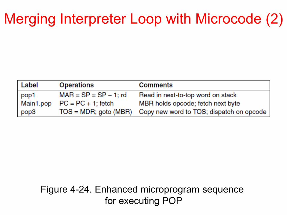
Merging Interpreter Loop with Microcode (2)
Figure 4-24. Enhanced microprogram sequence for executing POP
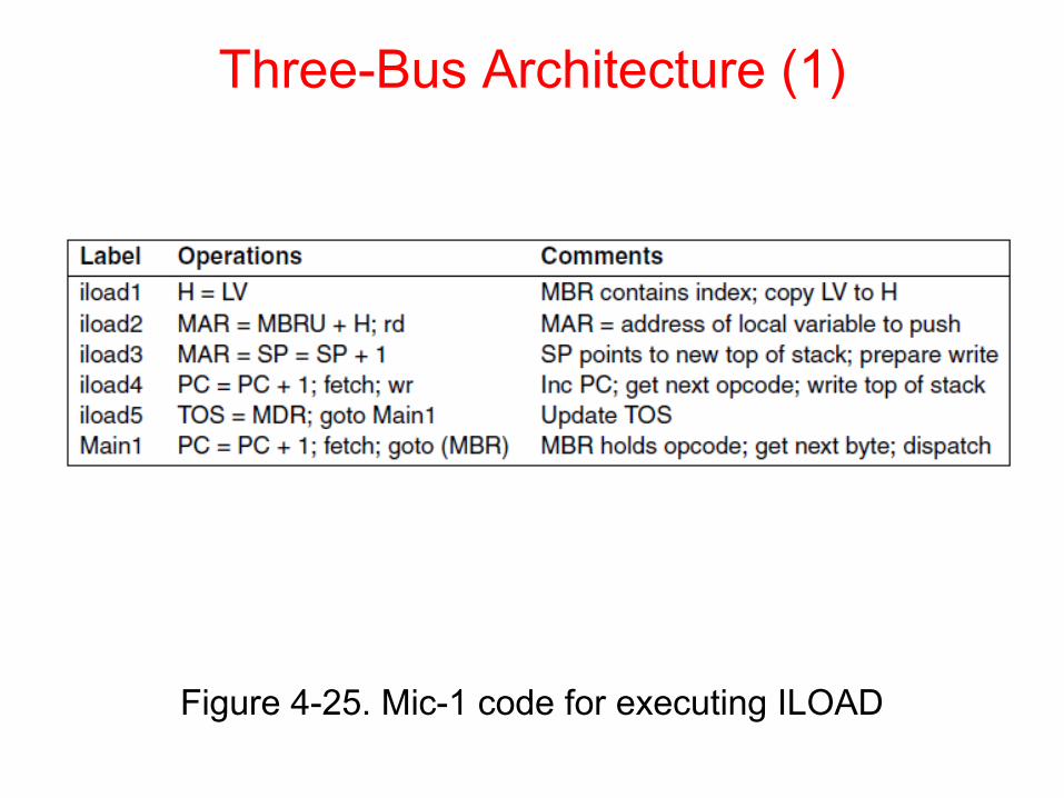
Three-Bus Architecture (1)
Figure 4-25. Mic-1 code for executing ILOAD

Three-Bus Architecture (2)
Figure 4-26. Three-bus code for executing ILOAD.

Instruction Fetch Unit (1)
For every instruction the following operations may occur:
• PC passed through ALU and incremented.• PC used to fetch next byte in instruction stream.• Operands read from memory.
• Operands written to memory.
• The ALU does computation and results stored back.

Instruction Fetch Unit (2)
Figure 4-27. A fetch unit for the Mic-1.

Instruction Fetch Unit (3)
Figure 4-28. A finite-state machine for implementing the IFU.

Design with Prefetching: The Mic-2 (1)
Figure 4-29. The data path for Mic-2.

Design with Prefetching: The Mic-2 (2)
Figure 4-29. The data path for Mic-2.
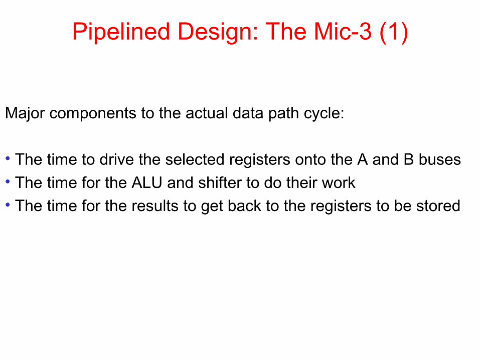
Pipelined Design: The Mic-3 (1)
Major components to the actual data path cycle:
• The time to drive the selected registers onto the A and B buses• The time for the ALU and shifter to do their work• The time for the results to get back to the registers to be stored

Pipelined Design: The Mic-3 (2)
Figure 4-30. The microprogram for the Mic-2 (part 1 of 3).
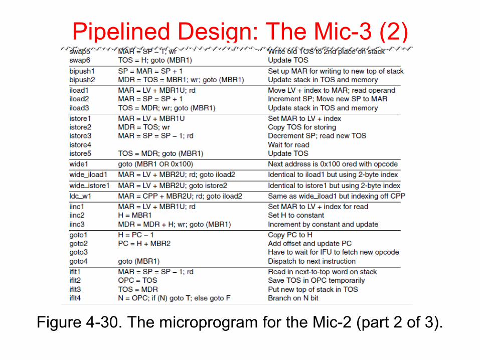
Pipelined Design: The Mic-3 (2)
Figure 4-30. The microprogram for the Mic-2 (part 2 of 3).

Pipelined Design: The Mic-3 (2)
Figure 4-30. The microprogram for the Mic-2 (part 3 of 3).

Pipelined Design: The Mic-3 (3)
Figure 4-31. The three-bus data path used in the Mic-3.

Pipelined Design: The Mic-3 (3)
Figure 4-31. The three-bus data path used in the Mic-3.

Pipelined Design: The Mic-3 (4)
Figure 4-32. The Mic-2 code for SWAP.

Pipelined Design: The Mic-3 (5)
Figure 4-33. The implementation of SWAP on the Mic-3.
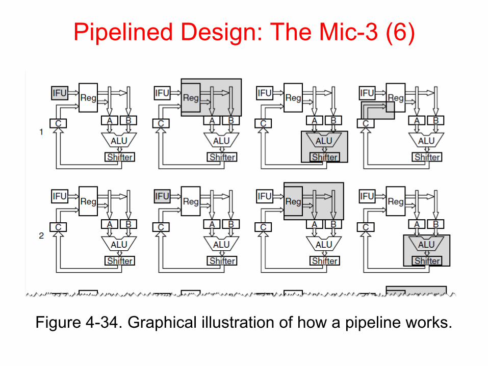
Pipelined Design: The Mic-3 (6)
Figure 4-34. Graphical illustration of how a pipeline works.
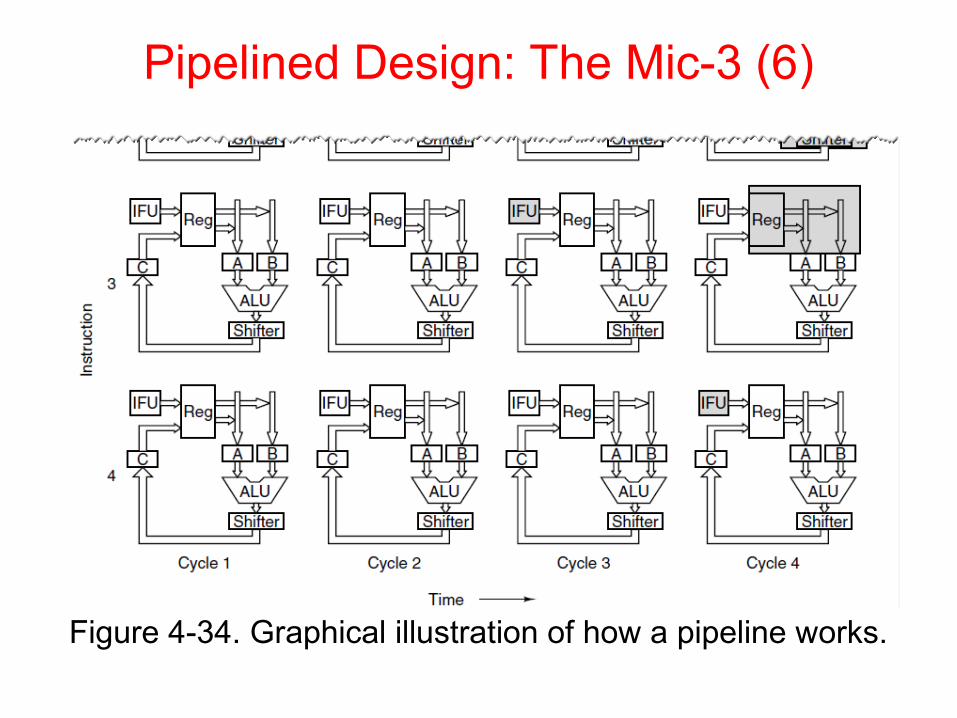
Pipelined Design: The Mic-3 (6)
Figure 4-34. Graphical illustration of how a pipeline works.

Seven-Stage Pipeline: The Mic-4 (1)
Figure 4-35. The main components of the Mic-4.

Seven-Stage Pipeline: The Mic-4 (2)
Figure 4-36. The Mic-4 pipeline.

Cache Memory
Figure 4-37. A system with three levels of cache.

Direct-Mapped Caches (1)
Each cache entry consists of three parts:
• Valid bit indicates whether there is any valid data in this entry
• Tag with unique, 16-bit value identifying corresponding line of
memory from which data came
• Data field contains copy of data in memory.
Holds one cache line of 32 bytes.

Direct-Mapped Caches (2)
Figure 4-38. (a) A direct-mapped cache. (b) A 32-bit virtual address.

Direct-Mapped Caches (3)
TAG field corresponds to Tag bits stored in cache entry.
LINE field indicates which cache entry holds corresponding data, if present.
WORD field tells which word within a line is referenced.
BYTE field usually not used, but if only single byte is requested, tells which byte within word is needed.
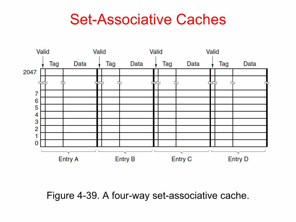
Set-Associative Caches
Figure 4-39. A four-way set-associative cache.

Branch Prediction
Figure 4-40. (a) A program fragment. (b) Its translation to a generic assembly language.

Dynamic Branch Prediction (1)
Figure 4-41. (a) 1-bit branch history. (b) 2-bit branch history. (c) Mapping between branch instruction address, target address.

Dynamic Branch Prediction (2)
Figure 4-42. A 2-bit finite-state machine for branch prediction.

Out-of-Order Execution, Register Renaming (1)
Figure 4-43. A superscalar CPU with in-order issue and in-order completion.
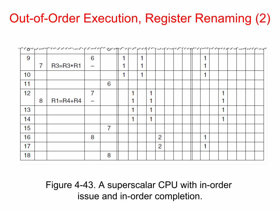
Out-of-Order Execution, Register Renaming (2)
Figure 4-43. A superscalar CPU with in-order issue and in-order completion.

Out-of-Order Execution, Register Renaming (3)
Figure 4-44. Operation of a superscalar CPU with out-of-order issue and out-of order completion.
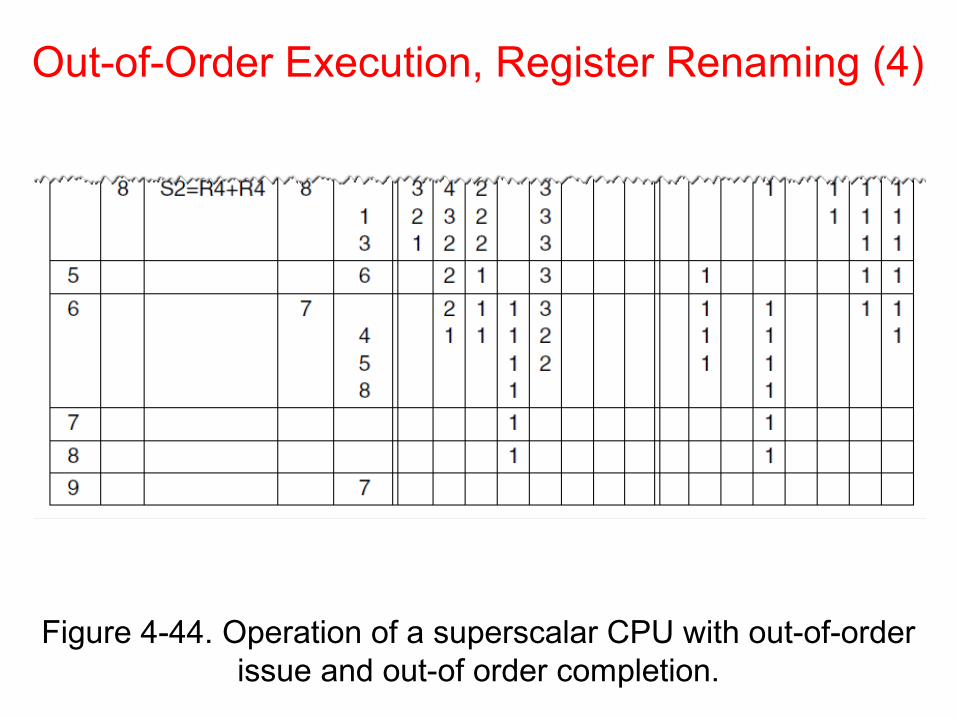
Out-of-Order Execution, Register Renaming (4)
Figure 4-44. Operation of a superscalar CPU with out-of-order issue and out-of order completion.
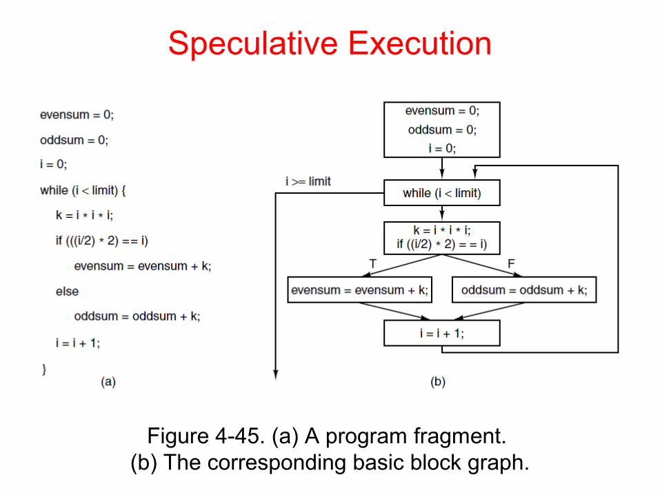
Speculative Execution
Figure 4-45. (a) A program fragment. (b) The corresponding basic block graph.

Core i7’s Sandy Bridge Microarchitecture
Figure 4-46. The block diagram of the Core i7’s Sandy Bridge microarchitecture.

Core i7’s Sandy Bridge Pipeline (1)
Figure 4-47. A simplified view of the Core i7 data path.
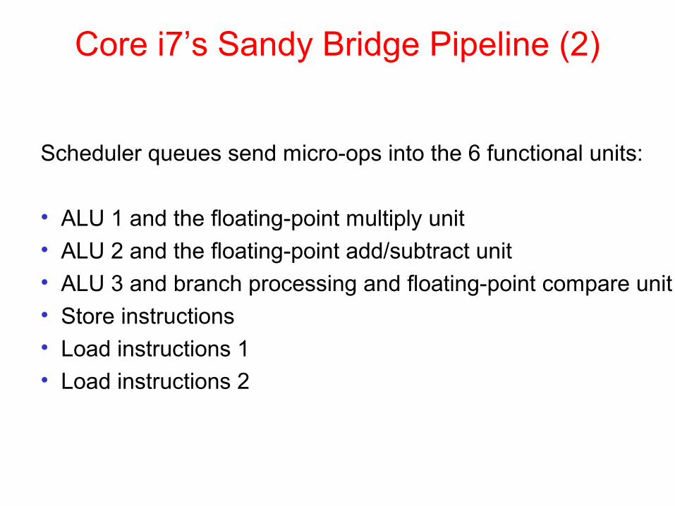
Core i7’s Sandy Bridge Pipeline (2)
Scheduler queues send micro-ops into the 6 functional units:
• ALU 1 and the floating-point multiply unit
• ALU 2 and the floating-point add/subtract unit
• ALU 3 and branch processing and floating-point compare unit
• Store instructions• Load instructions 1• Load instructions 2

OMAP4430’s Cortex A9 Microarchitecture
Figure 4-48. The block diagram of the OMAP4430’s Cortex A9 microarchitecture.

OMAP4430’s Cortex A9 Pipeline (1)
Figure 4-49. A simplified representation of the OMAP4430’s Cortex A9 pipeline.
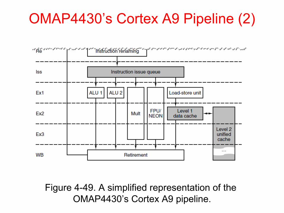
OMAP4430’s Cortex A9 Pipeline (2)
Figure 4-49. A simplified representation of the OMAP4430’s Cortex A9 pipeline.

Microarchitecture of the ATmega168 Microcontroller
Figure 4-50. The microarchitecture of the ATmega168.

End
Chapter 4