the role of (sub)-surface oxygen on the surface electronic structure of hydrogen terminated (100)...
TRANSCRIPT

ls 15 (2006) 687–691www.elsevier.com/locate/diamond
Diamond & Related Materia
The role of (sub)-surface oxygen on the surface electronic structure ofhydrogen terminated (100) CVD diamond
W. Deferme a,⁎, G. Tanasa b, J. Amir b, K. Haenen a,c, M. Nesládek a,c,d, C.F.J. Flipse b
a Hasselt University, Institute for Materials Research (IMO), Wetenschapspark 1, B-3590 Diepenbeek, Belgiumb Eindhoven University of Technology, Physics Department, Den Dolech 2, 5612 AZ Eindhoven, The Netherlands
c IMEC vzw, Division IMOMEC, Wetenschapspark 1, B-3590 Diepenbeek, Belgiumd CEA/Saclay, LIST (CEA-Recherche Technologique)/DETECS/SSTM/LTD, Bât 451, F-91191 Gif-sur-Yvette, France
Available online 20 February 2006
Abstract
In this work, scanning tunnelling microscopy (STM) and scanning tunnelling spectroscopy (STS) were applied to investigate the surfacemorphology and the surface electronic structure of plasma-treated (100)-oriented CVD diamond films. These films were hydrogenated using aconventional MWPE-CVD (microwave plasma enhanced chemical vapour deposition) reactor containing a H2 or a H2 /O2 mixture. A comparison ismade between (100)-oriented CVD diamond films hydrogenated with and without a small addition of oxygen (1%). X-ray PhotoelectronSpectroscopy (XPS) and UV Photoelectron Spectroscopy (UPS) measurements point to the presence of O-atoms at the (sub)-surface of the diamondfilm. The measured conductivity is significantly different for the two processes of hydrogenation. Annealing experiments point out that the samples,which were terminated using the H2 /O2 mixture are still conductive enough after annealing at 410 °C to enable STM experiments. Here, we discussthe mechanism for STM imaging of H2 /O2 treated diamond films, associated with surface states induced by the oxygen incorporation.© 2005 Elsevier B.V. All rights reserved.
Keywords: Diamond properties and applications; Surface conductivity; Scanning tunnelling spectroscopy; Oxygen plasma treatment
1. Introduction
Diamond surfaces terminated by hydrogen and subsequentinteractions of the hydrogenated diamond surfaces with ambientenvironment resulting in the p-type surface conductivity havebeen intensively studied in the past [1–6]. Maier et al. [7] gavethe first experimental evidence that chemisorbed hydrogen is anecessary but not a sufficient prerequisite for such surfaceconductivity and that the electron acceptors are provided byatmospheric adsorbates, leading to the so called “transfersurface doping” model. Oxygen can play an important role inthis process but its influence is not fully understood [8]. The aimof this paper is to elucidate further the mechanism responsiblefor the surface conductivity and the role of oxygen herein. Thiseffect is very promising because it can be used in futureelectronic and bioelectronic applications as has been demon-strated on laboratory scale [9–11].
⁎ Corresponding author. Tel.: +32 11 268874; fax: +32 11 268899.E-mail address: [email protected] (W. Deferme).
0925-9635/$ - see front matter © 2005 Elsevier B.V. All rights reserved.doi:10.1016/j.diamond.2005.12.016
Here, we report on hydrogenation of the diamond surfaceusing a H2 /O2 mixture during the microwave plasma enhancedsurface treatment. The XPS measurement confirms that oxygenis present at the diamond surface. Evidence is given for thebeneficial influence of oxygen on the stability of the surfaceconductivity upon annealing. Especially, even when diamond isannealed at UHV conditions and the atmospheric adsorbatelayer disappears, the remaining surface conductivity and surfacestates induced by the presence of oxygen are enough to enableSTM/STS measurements and imaging on the atomic resolutionscale. This is not the case for films hydrogenated in a pure H-plasma, where after annealing at about 400 °C in UHV, STM/STS measurements are not possible anymore.
2. Experimental
Single-crystal diamond layers are grown by using themicrowave plasma enhanced chemical vapour depositiontechnique (MWPE-CVD) on (100) Ib orientated HPHTdiamond substrates from Sumitomo Electric Ltd. Substrates
0 200 400 600 800 1000 1200
0
500
1000
1500
2000
2500
C
O
(a)Global XPS spectrum H2 termination
Cou
nts
BE (eV)
0 200 400 600 800 1000 1200
0
200
400
600
800
1000
1200
1400
O
C
(b)Global XPS spectrum H2/O2 termination
Cou
nts
BE (eV)
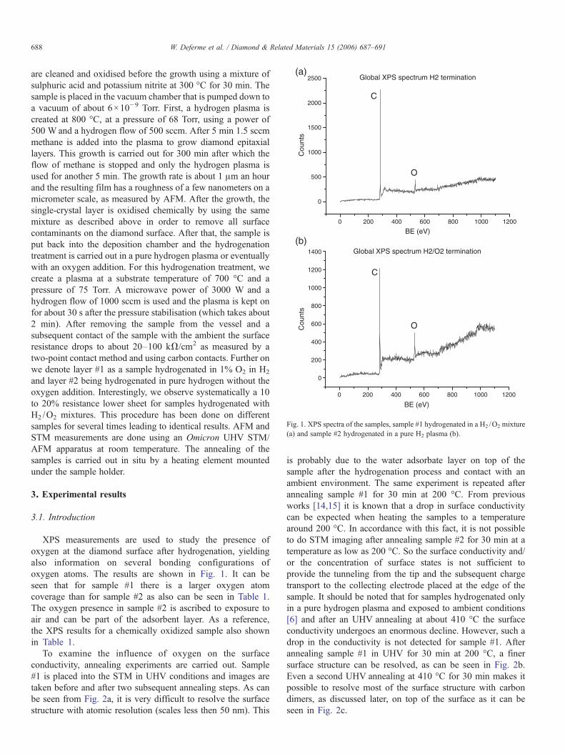
Fig. 1. XPS spectra of the samples, sample #1 hydrogenated in a H2 /O2 mixture(a) and sample #2 hydrogenated in a pure H2 plasma (b).
688 W. Deferme et al. / Diamond & Related Materials 15 (2006) 687–691
are cleaned and oxidised before the growth using a mixture ofsulphuric acid and potassium nitrite at 300 °C for 30 min. Thesample is placed in the vacuum chamber that is pumped down toa vacuum of about 6×10⁻⁹ Torr. First, a hydrogen plasma iscreated at 800 °C, at a pressure of 68 Torr, using a power of500 W and a hydrogen flow of 500 sccm. After 5 min 1.5 sccmmethane is added into the plasma to grow diamond epitaxiallayers. This growth is carried out for 300 min after which theflow of methane is stopped and only the hydrogen plasma isused for another 5 min. The growth rate is about 1 μm an hourand the resulting film has a roughness of a few nanometers on amicrometer scale, as measured by AFM. After the growth, thesingle-crystal layer is oxidised chemically by using the samemixture as described above in order to remove all surfacecontaminants on the diamond surface. After that, the sample isput back into the deposition chamber and the hydrogenationtreatment is carried out in a pure hydrogen plasma or eventuallywith an oxygen addition. For this hydrogenation treatment, wecreate a plasma at a substrate temperature of 700 °C and apressure of 75 Torr. A microwave power of 3000 W and ahydrogen flow of 1000 sccm is used and the plasma is kept onfor about 30 s after the pressure stabilisation (which takes about2 min). After removing the sample from the vessel and asubsequent contact of the sample with the ambient the surfaceresistance drops to about 20–100 kΩ/cm2 as measured by atwo-point contact method and using carbon contacts. Further onwe denote layer #1 as a sample hydrogenated in 1% O2 in H2
and layer #2 being hydrogenated in pure hydrogen without theoxygen addition. Interestingly, we observe systematically a 10to 20% resistance lower sheet for samples hydrogenated withH2 /O2 mixtures. This procedure has been done on differentsamples for several times leading to identical results. AFM andSTM measurements are done using an Omicron UHV STM/AFM apparatus at room temperature. The annealing of thesamples is carried out in situ by a heating element mountedunder the sample holder.
3. Experimental results
3.1. Introduction
XPS measurements are used to study the presence ofoxygen at the diamond surface after hydrogenation, yieldingalso information on several bonding configurations ofoxygen atoms. The results are shown in Fig. 1. It can beseen that for sample #1 there is a larger oxygen atomcoverage than for sample #2 as also can be seen in Table 1.The oxygen presence in sample #2 is ascribed to exposure toair and can be part of the adsorbent layer. As a reference,the XPS results for a chemically oxidized sample also shownin Table 1.
To examine the influence of oxygen on the surfaceconductivity, annealing experiments are carried out. Sample#1 is placed into the STM in UHV conditions and images aretaken before and after two subsequent annealing steps. As canbe seen from Fig. 2a, it is very difficult to resolve the surfacestructure with atomic resolution (scales less then 50 nm). This
is probably due to the water adsorbate layer on top of thesample after the hydrogenation process and contact with anambient environment. The same experiment is repeated afterannealing sample #1 for 30 min at 200 °C. From previousworks [14,15] it is known that a drop in surface conductivitycan be expected when heating the samples to a temperaturearound 200 °C. In accordance with this fact, it is not possibleto do STM imaging after annealing sample #2 for 30 min at atemperature as low as 200 °C. So the surface conductivity and/or the concentration of surface states is not sufficient toprovide the tunneling from the tip and the subsequent chargetransport to the collecting electrode placed at the edge of thesample. It should be noted that for samples hydrogenated onlyin a pure hydrogen plasma and exposed to ambient conditions[6] and after an UHV annealing at about 410 °C the surfaceconductivity undergoes an enormous decline. However, such adrop in the conductivity is not detected for sample #1. Afterannealing sample #1 in UHV for 30 min at 200 °C, a finersurface structure can be resolved, as can be seen in Fig. 2b.Even a second UHV annealing at 410 °C for 30 min makes itpossible to resolve most of the surface structure with carbondimers, as discussed later, on top of the surface as it can beseen in Fig. 2c.

VBM
Tunneling electrons
NEA
ψψ = 3,4 eV
O-states
CBM
EF
Evac
Tip Vacuum Sample
Fig. 3. Schematic diagram of the band bending model of the hydrogenateddiamond surface in a H2 /O2 mixture.
Table 1The surface coverage by oxygen in several bonding configurations calculatedfrom the XPS results
% C % O
H2/O2 termination 93 (±0.3) 7 (±0.3)H2 termination 96 (±0.4) 4 (±0.4)O2 termination (chemically) 88 (±0.7) 12 (±0.7)
The relative amounts of oxygen and carbon atoms detected in samples by XPSare shown for both samples #1 and #2 and for a reference sample, which hasbeen oxidized using a chemical oxidation discussed in the text. The precision forthe determination of carbon and oxygen concentration is 0.3% and 0.7%,respectively.
689W. Deferme et al. / Diamond & Related Materials 15 (2006) 687–691
The imaging is thus only possible for samples hydrogenatedin a H2 /O2 mixture, pointing to the presence of a sufficientlyconductive surface and at the same time to the presence ofsurface states to which electrons from the tip can tunnel which isa necessary prerequisite for STM imaging. From this, we canconclude that the oxygen that was used during the hydrogena-tion process of sample #1 has an important influence on thesurface conductivity and/or on the presence of surface states. Aschematic diagram, illuminating the principles for STMimaging via O-induced states are shown in Fig. 3 while thesurface band bending is discussed in detail below.
3.2. Surface morphology
STM/STS measurements performed on sample #1 areshown in detail in Fig. 4. Even though similar experimentshave been done before, there are several novelties in ourmeasurements compared to previous work [12,13]. Comparedto results of Dujardin and Bobrov [12,13] we use undoped H-terminated CVD diamond films (in all other published caseseither B-doped samples or clean surfaces with a Penneyreconstructed surface have been used for STM imagingproviding sufficient surface conductivity). Till now, as far aswe know it was not possible to carry out STM atomicresolution imaging on annealed H-terminated undopeddiamond films. The STM results for sample #1, shown inFig. 2, were taken using a tip bias Ubias=1.5 V and current
Fig. 2. STM images of the hydrogenated diamond surface #1 without annealing (a)30 min at 410 °C (c).
I=0.80 nA. The surface morphology imaging reveals a veryflat surface of the diamond epilayers (a few nanometersroughness on a scale of 10 μm). With an atomic resolution,dimers on top of the layer can be observed. These dimers arethe carbon atoms at the top layer, lying in one direction 5.044Å apart from the next dimers. Also the 2×1 reconstructioncan be seen, with dimers lying on terraces sized in the orderof 2 nm by 2 nm and rotated to each other by 90°.Measurements on sample #1 demonstrate that the size andorientation of the terraces is not influenced by the addition ofoxygen during the hydrogenation as similar results wereobtained for H-terminated B-doped diamond in Ref. [12].
Fig. 5 shows the I–V characteristics of the two samples. Ascan be seen, while the one of sample #2 exhibits a quasi-Ohmiccharacter with no surface bandgap, probably due to adsorptionof water — e.g. the H/H3O
+ terminated surface, which leads totunneling and current flow through the adsorbants (water) layer.Sample #1 has a surface bandgap of around 3.5 eV after UHVannealing to 410 °C. Fig. 5(c) shows the first and secondderivative of the I–V characteristics of the sample #1. Fig. 5cshows a resonance tunneling behaviour, similar to the one
, after UHV annealing for 30 min at 200 °C (b) and after UHV annealing for

Fig. 5. (a) The I–V characteristic of sample #2, showing a quasi-Ohmic character; (b)The derivative and second derivative of (b) showing a wave-like behaviour pointing
Fig. 4. The atomic resolution image of 2×1 reconstructed diamond surface ofsample #1, hydrogenated in H2 /O2 mixture and annealed in UHVat 410 °C for30 min.
690 W. Deferme et al. / Diamond & Related Materials 15 (2006) 687–691
observed for clean diamond surfaces in Ref. [12,13]. Never-theless, in our case, the surface resonances are observed for thehydrogenated surface, containing also residual oxygen atomswhile in ref [13], hydrogen-free, 2×1 reconstructed surfaceshave been studied. These resonances observed for H2 /O2
mixture treated diamond surfaces are observed for the first timeand will be discussed in another publication.
3.3. Discussion
The presence of levels in the surface bandgap, detected bySTS, implies that the tunnelling can occur to such states if at thesame time there is a sufficient electrical conductivity to collectthe carriers tunnelled from the STM tip into the surface states(see Fig. 3). This could be observed for sample #1. On the otherhand, for sample #2 there is not sufficient conductivity and/orconcentration of surface states to carry out STM experiments.Because STM imaging was possible for B-doped H-terminateddiamond surfaces [12,13] (e.g. there is a sufficient density of H-related surface states as reported in several publications [12]),
I–V characteristic of the hydrogenated sample #1 after UHVanneal at 410 °C; (c)to resonances with surface states.
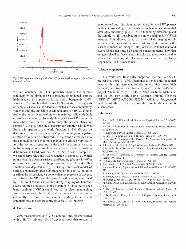
Fig. 6. UPS spectrum of sample #1 after UHVannealing showing the NEA of thediamond surface.
691W. Deferme et al. / Diamond & Related Materials 15 (2006) 687–691
we can conclude that it is probably mainly the surfaceconductivity that limits the STM imaging on undoped sampleshydrogenated in a pure H-plasma and subsequently UHV-annealed. This implies that for our H2 /O2 mixture hydrogenat-ed sample, as soon as the adsorbate related surface conductivityvanishes after the annealing at temperatures of 410 °C, anothermechanism takes over, leading to a remaining sufficiently highelectrical conductivity. To study this hypothesis UPS measure-ments have been carried out to study the surface states forsample #1. In Fig. 6 the He I spectrum for sample #1 is shown.From this spectrum, the work function ψ=3.4 eV can bedetermined. Further on, a typical peak pointing to negativeelectron affinity can be observed, i.e. electrons thermalised intothe conduction band minimum (CBM) are emitted very easilyinto the vacuum, appearing in the He I spectrum as a sharp,high-intensity peak at low kinetic energies. Its energy positiondetermines the CBM position [16–18]. So, in case of sample #1we can observe NEA and a work function of about 3.4 eV whichpoints towards upwards surface band bending (about −1.4 eV inour case determined from the position of the NEA peak). Thissituation was depicted in Fig. 3. Though the exact model ofsurface conductivity after a hydrogenation in a H2 /O2 mixtureis still under discussion, we believe that the presence of oxygen,as confirmed by XPS, and the upward band bending, confirmedby UPS, point towards a possible strong coupling of O-surfacestates, reported previously in the literature [8], into the valenceband maximum (VBM) could lead to the electron tunnelingfrom such states to the VBM, and the tunneled charge can beefficiently led out of the sample, leading to sufficientconductivities and consequently possible STM imaging.
4. Conclusion
XPS measurements on CVD diamond films, plasma-treatedwith a H2 /O2 mixture (1% of oxygen) show that oxygen is
incorporated into the diamond surface after the MW plasmatreatment. Annealing experiments on such samples, show thatafter UHVannealing up to 410 °C, a tunnelling between tip andthe sample is still possible, surprisingly enabling UHV-STMimaging. This allowed us to carry out STM imaging on H-terminated surfaces with atomic resolution and to monitor thesurface structure of undoped (100) oriented epitaxial diamondlayers for the fist time. STS and UPS measurements show thatoxygen-related surface states, lying close to the valence band towhich the tunneling of electrons can occur, are probablyresponsible for this mechanism.
Acknowledgements
This work was financially supported by the IWT-SBO-project No. 030219 “CVD Diamond: a novel multifunctionalmaterial for high temperature electronics, high power/highfrequency electronics and bioelectronics”, by the IAP-P5/01project “Quantum Size Effects in Nanostructured Materials”and the EU FP6 Marie Curie Research Training Network“DRIVE”, MRTN-CT-2004-512224. KH is a PostdoctoralFellow of the Research Foundation-Flanders (FWO-Vlaanderen).
References
[1] J.A. Garrido, T. Heimbeck, M. Stutzmann, Physical Review B 71 (2005)245310.
[2] J.P. Goss, P.R. Briddon, R. Jones, S. Sque, Diamond and Related Materials13 (2004) 684.
[3] H. Kawarada, Surface Science Reports 26 (1996) 205.[4] L. Ley, R. Graupner, J.B. Cui, J. Ristein, Carbon 37 (1999) 793.[5] S. Poykko, M. Kaukonen, M.J. Puska, R.M. Nieminen, Computational
Materials Science 10 (1998) 351.[6] J. Ristein, et al., Journal of Physics-Condensed Matter 13 (2001) 8979.[7] F. Maier, M. Riedel, B. Mantel, J. Ristein, L. Ley, Physical Review Letters
85 (2000) 3472.[8] K. Bobrov, H. Schechter, A. Hoffman, M. Folman, Applied Surface
Science 196 (2002) 173.[9] H. Kawarada, Surface Science Reports 26 (1996) 205.[10] J.A. Garrido, et al., Applied Physics Letters 82 (2003) 988.[11] J.A. Garrido, et al., Physica Status Solidi A-Applied Research 193 (2002)
517.[12] K. Bobrov, et al., Physical Review B 68 (2003) 195416.[13] K. Bobrov, A.J. Mayne, G. Dujardin, Nature 413 (2001) 616.[14] M. Riedel, J. Ristein, L. Ley, Physical Review B 69 (2004) 125338.[15] M. Cannaerts, et al., Physica Status Solidi A-Applied Research 186 (2001)
235.[16] A. Gali, J.E. Lowther, P. Deak, Journal of Physics-Condensed Matter 13
(2001) 11607.[17] L. Diederich, O. Kuttel, P. Aebi, L. Schlapbach, Surface Science 418
(1998) 219.[18] J.C. Zheng, X.N. Xie, A.T.S. Wee, K.P. Loh, Diamond and Related
Materials 10 (2001) 500.