the selective low cost gas sensor based on functionalized
TRANSCRIPT

HAL Id: tel-01488898https://pastel.archives-ouvertes.fr/tel-01488898
Submitted on 14 Mar 2017
HAL is a multi-disciplinary open accessarchive for the deposit and dissemination of sci-entific research documents, whether they are pub-lished or not. The documents may come fromteaching and research institutions in France orabroad, or from public or private research centers.
L’archive ouverte pluridisciplinaire HAL, estdestinée au dépôt et à la diffusion de documentsscientifiques de niveau recherche, publiés ou non,émanant des établissements d’enseignement et derecherche français ou étrangers, des laboratoirespublics ou privés.
The selective low cost gas sensor based on functionalizedgrapheneHeechul Woo
To cite this version:Heechul Woo. The selective low cost gas sensor based on functionalized graphene. Micro and nanotech-nologies/Microelectronics. Université Paris Saclay (COmUE), 2016. English. �NNT : 2016SACLX050�.�tel-01488898�

i
NNT : 2016SACLX050
THESE DE DOCTORAT DE
L‟UNIVERSITE PARIS-SACLAY PREPAREE A
“ECOLE POLYTECHNIQUE”
ECOLE DOCTORALE N°573 Interfaces : approches interdiscipliaires, fondements, applications et innovation
Spécialité de doctorat : Physique
Par
M Heechul Woo
Un capteur de gaz sélectif et bas coût par l‟emploi de graphène fonctionnalisé
Thèse présentée et soutenue à Palaiseau, le 29 septembre 2016 : Composition du Jury : M. Vanderbeek Kees Directeur de Recherche, Ecole Polytechnique Président Mme. Mayne Martine Directrice de Recherche, CEA Rapporteur M. Bourouina Tarik Professeur, ESIEE Rapporteur M. Mallah Talal Professeur, Université Paris-Sud Examinateur M. Legagneux, Pierre Directeur de Recherche, Thales R&T Examinateur M. Cojocaru Costel Directeur de Recherche, CNRS Directeur de thèse Mme. Bouanis Fatima Chargé de Recherche, IFSTTAR Co-directeur de thèse M. Chatellier Patrice Directeur de Recherche, IFSTTAR Invité

ii
Acknowledgement
My first arrival at LPICM (Laboratoire de Physique des Interfaces et des Couches
Minces) was in 2012 and I started my Ph.D thesis in 2013 after one and a half years of mater
courses. Therefore I have spent almost five years with all the people at LPICM, thus I have
many people to express my appreciation. I would like to remark the fact that thankful heart
toward people whom I worked with throughout the past five years stays all the same.
First of all, I would like to express the deepest gratitude to Costel-Sorin Cojocaru.
Not only as a director of NanoMaDe group but as my thesis director, his invaluable support
and guidance for the entire period of my study motivated and encouraged me to keep focus
on the thesis works. His insightful scientific advices often made a breakthrough for many
obstacles I have faced with. In particular, I admire his open-mindness in scientific attitude.
He listens to and respects others and induces meaningful discussion that serves as a great
source for constructing and developing scientific ideas.
I also thank to Patrice Chatellier, director of LISIS (Laboratoire Instrumentation,
Simulation et Informatique et Scientifique). From the very beginning of the thesis, he has
spared no effort to lend a hand on everything required to complete the thesis. I also deeply
appreciate to my thesis superviser, Fatima Zahra Bouanis. Her kind and considerate care
allows me all the best options to take advantage of.
I want to extend my gratitude to Pere Roca i Cabarrocas, the director of LPICM for
providing me this great chance to do research. I‟m grateful to Yvan Bonnassieux for his
considerable assistance from the early settlement in France.
I thank to all my past and present fellow researchers, Leandro Nicolás Sacco, Waleed
Moujahid, Fulvio Michelis, Ileana Florea, Garry Rose Kitchner, Éléonor Caristan (Leo), for
their continuous support in research part with collaborative and enjoyable environment.
Also special thanks to Korean friends who have finished or are studying for their
dorctor/master degree at Ecole Polytechnique, Kahyun Kim, Changseok Lee, Kihwan Kim,
Jongwoo Jin, Taewoo Jeon, Changhyun Kim, Jinwoo Choi, Taeha Hwang, Kihwan Seok,
Hojoong Kwon, Sungyeop Jung, Heejae Lee, Jongyoon Park, Haena Won, Gijun Seo,

iii
Seonyong park, Sanghyuk Yoo, Jiho Yoon, Wonjong Kim, Dongcheon Kim, Heetae park,
Jejune Park, Heeryung Lee, Mintae Jung, Yongjeong Lee, Jeongmo Kim, Songyi Han.
Finally, I would like to express my heartfelt love and sincere gratitude to my family
in Korea and ma chérie, Deubora.

iv
Contents
Acknowledgement ......................................................................................................................................................................... ii
List of Abbreviation .................................................................................................................................................................. viii
Résumé en Français ..................................................................................................................................................................... 1
Chapter I.Introduction ................................................................................................................................................................ 6
1.1 Overview .......................................................................................................................................................................... 6
1.2 Graphene: Carbon allotropes, Properties and Applications ......................................................................... 9
1.2.1 Carbon Allotropes ................................................................................................................................... 9
1.2.2 Graphene properties ............................................................................................................................. 10
1.2.2.1 Electronic band structure of graphene ........................................................................................... 10
1.2.2.2 Electrical Properties ........................................................................................................................... 14
1.2.3 Graphene for device applications ..................................................................................................... 15
1.2.3.1 Graphene based electrode ................................................................................................................. 15
1.2.3.2 Graphene based transistor ................................................................................................................ 16
1.2.3.3 Graphene for Battery ......................................................................................................................... 16
1.2.3.4 Graphene for photonic devices ........................................................................................................ 17
1.2.3.5 Graphene for gas sensing applications .......................................................................................... 18
1.3 Functionalized graphene ......................................................................................................................................... 23
1.3.1 Covalent functionalization ................................................................................................................. 23
1.3.2 Non-covalent functionalization ......................................................................................................... 24
1.4 Conclusions .................................................................................................................................................................. 27
References ........................................................................................................................................................................... 29

v
Chapter II. Graphene Preparation and Characterization .......................................................................................... 41
2.1 Generalities .................................................................................................................................................................. 41
2.2 Preparation .................................................................................................................................................................. 42
2.2.1 Exfoliated graphene ............................................................................................................................. 42
2.2.2 Epitaxial graphene ................................................................................................................................ 43
2.2.3 CVD graphene ...................................................................................................................................... 44
2.2.3.1 PECVD ................................................................................................................................................ 46
2.2.3.2 Transfer of Graphene ....................................................................................................................... 46
2.3 Characterization techniques .................................................................................................................................. 48
2.3.1 Scanning Electron Microscopy (SEM) ............................................................................................ 48
2.3.2 Atomic Force Microscopy (AFM).................................................................................................... 49
2.3.3 Raman spectroscopy ............................................................................................................................ 50
2.3.4 Photoemission spectroscopy (PES) .................................................................................................. 51
2.3.4.1 Generalities .......................................................................................................................................... 51
2.3.4.2 X-ray Photoelectron Spectroscopy (XPS) .................................................................................... 52
2.3.4.3 Ultraviolet Photoelectron Spectroscopy (UPS) ........................................................................... 53
2.3.4.4 Angle-resolved photoemission spectroscopy (ARPES) ............................................................ 53
2.3.4.5 Auger electron spectroscopy (AES) ............................................................................................... 56
2.3.4.6 Electron energy loss spectroscopy (EELS) .................................................................................. 56
2.4 Conclusions .................................................................................................................................................................. 58
Reference ............................................................................................................................................................................. 60

vi
Chapter III. Prepared Graphene .......................................................................................................................................... 67
3.1 Prepared graphene .................................................................................................................................................... 67
3.1.1 PECVD interfacial graphene growth (LPICM) ............................................................................. 68
3.1.2 Epitaxial graphene (LPN) ................................................................................................................... 70
3.2 Graphene Characterization ................................................................................................................................... 71
3.3 Conclusions .................................................................................................................................................................. 73
Reference ............................................................................................................................................................................. 74
Chapter IV. Electrical Characterization ............................................................................................................................ 77
4.1 Device fabrication ...................................................................................................................................................... 77
4.1.1 Generalities ............................................................................................................................................ 77
4.1.2 Graphene (interaction) on the substrate........................................................................................... 77
4.1.3 Contact electrode deposition .............................................................................................................. 78
4.1.3.1 Inkjet printing ...................................................................................................................................... 79
4.1.3.2 Photo-lithography ............................................................................................................................... 80
4.1.3.3 Shadow-mask metal Evaporation ................................................................................................... 81
4.2 Four-electrode electrical measurements ............................................................................................................ 82
4.2.1 Four-probe measurement .................................................................................................................... 82
4.2.2 Four-electrode measurement ............................................................................................................. 86
4.3 O2, H2O desorption .................................................................................................................................................... 89
4.4 Light exposure response .......................................................................................................................................... 91
4.5 Humidity response ..................................................................................................................................................... 95
4.5.1 Humidity response of the device ...................................................................................................... 95
vii
4.5.2 Vacuum annealing effect .................................................................................................................... 97
4.5.3 Surface analysis .................................................................................................................................... 98
4.5.4 Mechanisms of humidity response ................................................................................................. 101
4.6 Conclusions ................................................................................................................................................................ 106
Reference ........................................................................................................................................................................... 107
Chapter V. Functionalization ............................................................................................................................................... 111
5.1 Generalities ................................................................................................................................................................ 111
5.2 Ruthenium Complex(Blue) ................................................................................................................................... 111
5.3 Functionalization of the device ........................................................................................................................... 114
5.3.1 Functionalization of the device ....................................................................................................... 114
5.3.2 Photoresponse of the functionalized device ................................................................................. 114
5.4 Double interfaces responses ................................................................................................................................. 121
5.4.1 Inversed response. .............................................................................................................................. 126
5.4.1.1 Intensity dependency of the inversed response under vacuum.............................................. 126
5.4.1.2 Duty cycle dependency of the inversed response under vacuum .......................................... 128
5.4.2 Charge transfer .................................................................................................................................... 130
5.5 Conclusions ................................................................................................................................................................ 135
Reference ........................................................................................................................................................................... 136
VI. Conclusions & Perspectives .......................................................................................................................................... 140

viii
List of Abbreviation
Acronym VOCs
CG
MS
CNTs
ITO
UV
LED
TFT
FET
SWIR
NIR
MIR
FIR
THz
SWF
SAW
QCM
MEMS
BAW
CVD
GO
RGO
PBSA
SEM
TEM AFM
PES
volatile organic compounds
chromatography
mass spectrometry
carbon nanotubes
indium tin oxide
ultraviolet
light emitting diode
thin film transistor
field-effect transistor
short-wave infrared
near-infrared
mid-infrared
far-infrared
terahertz
surface work function
surface acoustic wave quartz crystal microbalance
micro electromechanical systems
bulk acoustic wave
chemical vapor deposition
graphene oxide
reduced graphene oxide
pyrene butanoic acid succidymidyl ester
scanning electron microscopy
transmission electron microscopy
atomic force microscopy
photoemission spectroscopy

ix
Acronym HOPG
GICs
SiC
FETs
CVD
SLG
PECVD
DI
UPS ARUPS XPS PMMA UHV IPA MLG
SDG
MLG
PR
Id
RH
AES
EELS
ECL
GO
ICMMO
MLCT
Highly Oriented Pyrolytic Graphite
graphite intercalate compounds
silicon carbide field effect transistors chemical vapor deposition single layer graphene plasma enhanced CVD
deionized
ultraviolet photoemission
angle-resolved investigation of valence band states
X-ray photoemission spectroscopy
polymethyl methacrylate ultra high vacuum isopropyl alcohol multi-layer graphene
single and double layer graphene
multi-layer graphene
photo-resist
drain current
relative humidity
Auger electron spectroscopy
electron energy loss spectrum
electrogenerated chemiluminescence
graphene oxide
Institut de Chimie Moléculaire et des Matériaux d‟Orsay Metal to Ligand Charge Transfer

1
Résumé en Français
Les progrès récents dans les nanomatériaux présentent un fort potentiel pour la
réalisation de capteurs de gaz avec de nombreux avantages tels que: la grande sensibilité de
détection de molécule unique, le faible coût et la faible consommation d'énergie. Le graphène,
isolé en 2004, est l'un des meilleurs candidats prometteurs pour le développement de futurs
nanocapteurs en raison de sa structure à deux dimensions, sa conductivité élevée et sa grande
surface spécifique. Chaque atome de la monocouche de graphène peut être considéré comme
un atome de surface, capable d'interagir même avec une seule molécule de l'espèce gazeuse
ou de vapeur cible, ce qui conduit finalement à un capteur ultrasensible.
Dans cette thèse, un capteur résistif à base de graphène fonctionnalisés a été fabriqué.
Le dispositif est basé sur le graphène monocouche sur substrat SiO2 fonctionnalisé avec Ru
complexes(II). Pour comprendre la réponse intrinsèque du film de graphène, un dispositif non
fonctionnalisée est d'abord étudié. La réponse du dispositif est sensible à l'environnement de
mesure telles que la pression, l'humidité relative et la lumière. Une fois la réponse intrinsèque
de l'appareil a été étudié, les dispositifs basés sur le graphène fonctionnalisés ont été
fabriqués pour mieux comprendre l'effet de la fonctionnalisation. Deux configurations
différentes ont été utilisées; le dispositif fonctionnalisé avec des complexes après le dépôt des
électrodes et le dispositif fabriqué en utilisant la surface pré-fonctionnalisé graphène. La
réponse de dispositif sous la lumière a été amélioré ou inversé en fonction de sa configuration.
Pour élucider ces réponses, les mécanismes du transfert de charge entre les complexes et le
dispositif ont été proposées.
Plusieurs types de films de graphène ont été préparés et caractérisés. En LPICM, le
graphène est directement synthétisé sur les substrats isolants en utilisant le système de
PECVD. Graphène synthétisés par CVD et transférées à SiO2 sont fournis par Thales R & T
tandis que le graphène épitaxiale sur SiC est fourni par LPN. Graphène commercial
synthétisé par CVD est également acheté. La plupart des performances des dispositifs à base
de graphène dépendent fortement de ses conditions de surface. Afin de minimiser les
caractéristiques inattendues provenant de différentes conditions de surface, le graphène
monocouche sur substrat SiO2 est finalement choisi en tant que matériau principal utilisé dans
la fabrication du dispositif.

2
La deuxième étape de la fabrication du dispositif est le dépôt des électrodes sur la
surface de graphène. Trois approches différentes ont été explorées; jet d'encre d'impression,
photo-lithographie et évaporation. En raison de sa complexité et de contaminations possibles
à travers le processus, photo-lithographie est exclue. L'impression par jet d'encre promet un
processus simple à faible coût, mais le choix limité dans les métaux ne sont pas favorables
pour la fabrication de dispositif. L‟évaporation de métal est principalement utilisé comme une
méthode de dépôt des électrodes dans ce travail. Avec un masque perforé simple, Ni, Co, Cr /
Au, Ni / Au et du Ti / Au électrodes ont été déposés avec succès sur la surface de graphène
préparée. L'optimisation des électrodes de dépôt peut être une question intéressante en termes
de fabrication du dispositif. Par exemple, la forme et la taille des électrodes et le choix du
métal sont des options possibles pour optimiser. Bien que CVD graphène promet la grande
surface pour la production de masse de dispositifs, il est polycristallin dans la nature et donc
des joints de grains perturbent le transport de charge. En outre, des contaminations de surface
à travers le processus sont également préjudiciables au transport de charge du film de
graphène. Dans le présent travail, pour faire une moyenne sur ce type de transport limitée
défavorable de charge, les électrodes avec 100 μm qui dépasse la taille du grain général de
quelques micromètres sont réalisées.
La réponse du dispositif est caractérisé en mesurant la résistance du dispositif. Le
concept de la mesure à quatre points est dévelopé pour tenir compte de la forme des
électrodes de dispositif et de caractériser le dispositif de façon plus précise. La résistance du
dispositif est contrôlée en fonction du temps pour que les changements d'état externes
peuvent être directement détectés et interprétés. La réponse du dispositif est simplement
exprimé sous la forme des variations de la résistance du dispositif, △R/R0.
La réponse intrinsèque du dispositif est étudié. La réponse du dispositif change lors
de l'adsorption / désorption de molécules d'eau et d'oxygène. Désorption de ces molécules
sous vide (10-5 mbar) a causé augmentation de plus de 6% en réponse. Ceci est dû à la dé-
dopage du film de graphène résultant de l'augmentation de la résistance du dispositif.
Désorption des molécules d'eau et d'oxygène peut être en outre accélérée sous l'illumination
de la lumière bleue 455 nm avec une intensité de 4 mW/cm2. Dans ce cas, la réponse du
dispositif augmente jusqu'à 40%. Étant donné que les résultats montrent que

3
l'adsorption/désorption de molécules d'eau et d'oxygène provoquent des variations sensibles
de réponse du dispositif, on peut facilement penser que les changements de réponse de
l'appareil lors de la variation relative du niveau d'humidité. A cause du renforcement du
dopage par adsorption des molécules d'eau, la réponse du dispositif diminue à mesure que le
niveau d'humidité augmente. Cependant, la réponse d'humidité inversée après le recuit sous
vide du dispositif à 150 °C pendant 90 minutes. Sur la base des résultats des diverses
techniques de PES les mécanismes responsables de deux réponses d'humidité différentes sont
proposées. L'adsorption des molécules d'eau sur la surface de graphène et les liaisons
hydrogène entre les molécules d'eau et les groupes fonctionnels restants sur le film de
graphène sont deux facteurs en compétition responsables de l'élucidation du mécanisme. Les
études sur la réponse intrinsèque du dispositif fournissent une compréhension préliminaire
pour un capteur de gaz par l‟emploi de graphène. Il convient de noter que les effets de l'air
ambiant doivent être pris en compte avant de caractériser le comportement de détection de
gaz.
Le capteur résistif sur la base du film de graphène fonctionnalisés avec des [RuII-
Pyr]2+ complexe de manière non covalente a été fabriquée. La fonctionnalisation non
covalente est appliquée afin d'éviter de modifier les structures électroniques indigènes et de
préserver les propriétés intrinsèques du graphène. La réponse du dispositif à la lumière (455
nm) améliorée et rapide a été obtenue qui n‟est pas observables avec un dispositif non-
fonctionnalisé. Les électrons transférés des Ru(II) complexes excités aux film de graphène
sous la lumière ont amélioré la réponse du dispositif tandis que la photo-désorption de
molécules d'eau et d'oxygène adsorbé sur la surface est responsable d'une augmentation lente
et globale de la réponse.
L'inversion de la photoréponse a été observée avec un dispositif à double interface
qui est fabriqué en déposant quatre électrodes identiques à la surface de graphène pré-
fonctionnalisée. La première interface est entre la couche d'adhérence de l'électrode
métallique et le Ru(II) complexe tandis que la seconde interface est entre le Ru(II) complexe
et le graphène. Le mécanisme proposé responsable de l'inversion de la réponse est basée sur
les variations de l'orientation des flux de transfert de charges. Au début, les électrons sont
transférés de Ru(II) complexes excités à graphène alors qu'ils se sont rendus à vers la couche

4
oxydée d'adhérence après la mesure continue et répété sous la lumière.
Pour conclure, les approches théoriques et expérimentales et les résultats obtenus au
cours de cette thèse ouvrent un moyen de comprendre et de fabriquer le futur captuer de gaz
par l‟emploi de graphène fonctionnalisé de façon non covalente.

5
Chapter I
Introduction
Chapter I.Introduction ............................................................................................................................. 6
1.1 Overview ........................................................................................................................................... 6
1.2 Graphene: Carbon allotropes, Properties and Applications .............................................................. 9
1.2.1 Carbon Allotropes ..................................................................................................................... 9
1.2.2 Graphene properties ................................................................................................................ 10
1.2.2.1 Electronic band structure of graphene ............................................................................ 10
1.2.2.2 Electrical Properties ........................................................................................................ 14
1.2.3 Graphene for device applications ............................................................................................ 15
1.2.3.1 Graphene based electrode ............................................................................................... 15
1.2.3.2 Graphene based transistor ............................................................................................... 16
1.2.3.3 Graphene for Battery ...................................................................................................... 16
1.2.3.4 Graphene for photonic devices ....................................................................................... 17
1.2.3.5 Graphene for gas sensing applications............................................................................ 18
1.3 Functionalized graphene ................................................................................................................. 23
1.3.1 Covalent functionalization ...................................................................................................... 23
1.3.2 Non-covalent functionalization ............................................................................................... 24
1.4 Conclusions ..................................................................................................................................... 27
References ............................................................................................................................................. 29
6
Chapter I.Introduction
1.1 Overview
The modern advanced technology and the global development of industrial activities
has been accompanied by a variety of serious environmental problems. One example is the
release of various chemical pollutants such as NOx, SOx, COx and volatile organic
compounds (VOCs) into the atmosphere caused from various manufacturing industries and
fossil fuel consumption of private sectors resulting in global environmental air pollution.
Air pollution can cause severe problems related to human health and environment. It
can simply cause, for example, a disease like asthma. Asthma is a disease affecting the
airways that carry air to and from the lungs. It is estimated that the total cost of asthma in
Europe is 19.3 billion euros per annum [1]. Another example of the consequence of air
pollution is acid rain. Any industrial and private activities resulting in the emissions of nitric
and (NOx) sulfuric acids (SOx) are responsible for acid rain. It usually erodes buildings and
affects human health through the contamination of water and harmed vegetation [2].
In addition to air pollution, the release of combustible gases such as methane, ethane,
butane, hydrogen and acetylene can also constitute significant risks in terms of possible
explosions of plants [3,4]. This sort of industrial accident not only leaves industrial damages
but also threats civil security.
To minimize the above stated damages, the development of new sensing platforms
and technologies to be used in real world for detecting and quantifying environmental
pollution, especially toxic and combustible gases are required [5]. Optical spectroscopy and
gas chromatography/mass spectrometry (CG/MS) are well-known analytic instruments that
have been widely used for air pollutant measurements. Although these instruments can give a
precise analysis, they are time-consuming, expensive, and can seldom be used in real-time in
the field. Gas sensors that are compact, robust, with versatile applications and a low cost are
needed. To meet this demand, considerable research into new sensors is underway, including
efforts to enhance the performance of traditional devices, such as gas sensors based on
semiconductor (Si) structures [6,7]. Numerous materials have been reported to be usable as
semiconductor sensors including both single- (e.g., ZnO, SnO2, WO3, TiO2 and Fe2O3) and

7
multi-component oxides (BiFeO3, MgAl2O4, SrTiO3, and Srl-yCayFeO3-x) [8]. Such devices
were applied to detect hydrogen [6,7], oxygen [9,10], carbon monoxide [9,10], hydrogen
sulfide [11], or as active element of smoke detectors [12]. However, this type of sensors are
generally limited by their high operating temperature (150-600 ˚C).
Recent advances in nanomaterials provided a strong potential to create a gas sensor
with many advantages including a very high sensitivity down to single molecule detection,
low cost, and low power consumption. This is well reflected by the fact that nanosensor
arrays are already under development by giant firms such as Dow Corning, Samsung, Boeing,
Lockheed Martin, IBM, and Agilent. Among nanomaterials, graphene that was first isolated
in 2004 [13], is one of the best promising candidate for the future development of
nanosensors applications because of its atom-thick, two-dimensional structures, high
conductivity, and large specific surface areas [14-18]. Every atom of a monolayer graphene
can be considered as a surface atom, capable of interacting even with a single molecule of the
target gas or vapor species, which eventually results in an ultrasensitive sensor response. The
potential advantages of graphene based sensor, in short, are that it can be ultra-compact,
effective at room temperature, characterized by low-power consumption, low cost, high
sensitivity, selectivity and with a very low response and recovery time.
However, despite its great potential abilities as a sensing material, graphene still face
some difficulties to be overcame for development of its practical use in sensing applications
such as large area homogeneous production, contacting and devices integration, selective
sensing mechanisms and so on. Since its discovery, there have been many efforts to improve
its quality and to synthesize large area homogeneous layer [77,81,90] and more, recently,
there are also many trials to functionalize graphene with various elements to improve its
sensitivity, specificity, solubility, loading capacity, etc [97-104]. Keeping step with this
tendency, this thesis tries to further develop the graphene based gas sensor by non-covalent
functionalization of its surface. The main purpose of functionalizing the surface of graphene
is to improve its specificity for selective sensing of the device. We have tried to reach this
objective by exploring functionalization of graphene via an organometallic complex. Such
approach can allow (via appropriate choice of the functionalizing complex) to each type of
gas to interact in a specific way with each metal, changing in a specific way the graphene

8
resistivity thus acting as fingerprinting for identifying the targeted gases.
The following chapters will describe the development of our graphene based gas
sensor. In Chapter 1, after this overview, we review the fundamental properties and various
applications of graphene. The preparation methods of graphene are then stated in Chapter 2
followed by the introduction of various graphene layer characterization techniques. In
Chapter 3, graphene layers used in our experiments are introduced with their preparation and
characterization. Chapter 4 explains the theoretical backgrounds of the electrical
characterization of our device in details with obtained experimental results. Chapter 5
describes the functionalization methods utilized in our experiment and the experimental
results obtained from functionalized graphene based device. The conclusion summarizes this
thesis and give an outlook for graphene based sensor.
9
1.2 Graphene: Carbon allotropes, Properties and Applications
1.2.1 Carbon Allotropes
Graphite, whose name stems from the Greek word “graphein” meaning to draw or
write, is now losing his authority in regard of writing and documentation. Times have
changed and the manner of writing and keeping documents has been changed as well. Today,
it seems even more natural to type a letter looking at the computer monitor rather than to
write it traditionally on the paper holding a pencil. On the other hand, given their exceptional
physical and electrical properties, graphene and carbon nanotubes (CNTs) have been trying to
take back so-called carbon allotropes‟ authority in various scientific fields in recent years.
Carbon exists in several forms called allotropes and diamond is one of them with a
very strong crystal lattice. Graphite is another well-known carbon allotrope in which the
graphene layers are stacked to form 3D structure. In 1985, another allotrope called
fullerenes(C60) was discovered by Kroto et al [19]. Its structural closed ball shape guides us
to the 0-dimensional electronics. In 1991, CNTs were observed by Iijima‟s group [20]. As its
name suggests, CNTs are made of rolled up graphene layers forming 1-dimensional tube
structure. The individual graphene layer, a 2-dimensional flat layer of carbon atoms highly
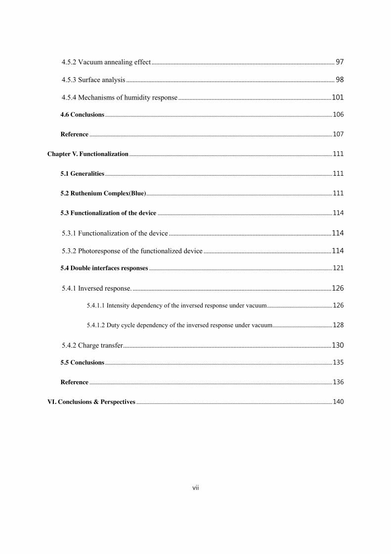
packed into honeycomb lattice and is a building block of the other allotropes as shown in the
(Figure 1.1.), was first isolated by Manchester group [13] in 2004.
Figure 1.1. Graphene as a building blocks for graphitic materials.

10
1.2.2 Graphene properties
Since its discovery, graphene has been an appealing and attractive material for many
researchers due to its exceptional properties. It is optically transparent (~97.7% transparency
for visible light) [21], mechanically robust (Young‟s modulus of 1.0TPa and stiffness of 130
GPa) [22] and it has high thermal conductivity (~6,000 W/mK) [22] as well. The
attractiveness becomes even amplified when it comes to its excellent electrical properties.
Theoretically, it has extremely high charge mobility (~200,000 cm2/Vs) at room temperature
which is about 200 times higher than that of Si. A very low resistivity (10-6 Ωcm), even less
than that of silver, was observed for the suspended graphene as well [23]. It can also carry
high current density up to 3x10⁸ A/cm2 [24]. The origin of such unique properties of graphene
will be explained by understanding its electronic band structure.
1.2.2.1 Electronic band structure of graphene
As its atomic number on the periodic table implies, carbon has 6 electrons. Then the
ground-state electron configuration of carbon atom can be represented as 1s22s22p2 where 2
electrons are filling the inner shell while the other 4 are occupying outer shell. The
combination of one 2s atomic orbital and two 2p atomic orbitals forms three equivalent sp2
hybrid orbitals and carbon atoms use this sp2 hybrid orbitals to form covalent bonds with
each other when they are constructing graphitic materials like graphite, graphene and CNTs
(Figure 1.2.). Three sp2 hybrid orbitals lie in a plane and the angle between them is 120°
while the third 2p atomic orbital consists of two lobes lying perpendicular to that plane.
In graphene, the overlap of these sp2 hybrid orbitals in plane forms the sigma(σ)
bond between the carbons atoms leading to the honeycomb lattice formation while remaining
2p orbitals on adjacent carbon atoms perpendicular to the plane overlap to form delocalized
pi(π) bond. Since they are much closer to the Fermi surface than σ electrons, π electrons are
responsible for charge carrier transport of graphene and determine the electronic properties of
graphene at low energy.

11
Figure 1.2. (a) Hybridized three sp2 orbitals for a carbon atom and (b) an unhybridized 2p
orbital
Figure 1.3. shows the typical honeycomb lattice of graphene with unit vectors in real
space and the reciprocal lattice space. The distance between two nearest carbon atoms acc is
estimated to be 0.142 nm [25]. As shown in the Figure 1.3.(a), the honeycomb lattice in real
space can be expressed with two sub lattices A and B of the triangular Bravais lattices [26].
Based on the Figure 1.3.(a), the unit cell vectors a1 and a2 can be expressed as
(
√ ) (
√ ) (1)
where acc = 0.142 nm is the distance between two nearest carbon atoms [25].
Corresponding reciprocal lattice vectors b1 and b2 can then be express as
(
√
) (
√
) (2)
For deriving electronic band structure of graphene can be we account the reciprocal
lattice of the triangular lattice. The shaded region in the Figure 1.3.(b) is the first Brillouin
zone (BZ) of graphene where Gamma point (Γ) corresponds to its center while K points on its
corners represent Dirac points.

12
Figure 1.3. (a) Schematic of honeycomb lattice of graphene with the unit vectors a1 and a2.
(b) Reciprocal lattice with Brillouin zone (BZ) where b1 and b2 are the reciprocal vectors.
In 1947, the first tight-binding model of graphene was reported by Wallace [27]
concerning the nearest and next-nearest neighbor interactions for 2p orbitals. Saito et al. in
1998 reported advanced tight binding approximation by expanding conventional model with
the wave function overlap of different atoms [28]. Based on their calculation that takes only
the nearest neighbor interactions into account, the energy dispersion relation in graphene can
be obtained
( ) √ √
(3)
where denotes the transfer integral between nearest neighbor so that the energy has the
values of , and 0 at the high symmetry points, Γ, M and K in the BZ respectively.
Energy dispersion of graphene can be visualized by plotting above equation. Figure
1.4.(a) represents the energy as a function of wave vectors produced by MATLAB with

13
=2.8 eV and the lattice constant, √ . As we can see, conduction band and valence
band are touching at Dirac points which is well consistent with the zero energy value
calculated at K points. At these Dirac points, intrinsic graphene can be considered as a zero
band gap semiconductor with the linear energy dispersion relation (Figure 1.4.(b)). Such
linear dispersion relation near these Dirac points provides most of interesting electronic
properties of graphene and it can be described as
( ) | | (4)
where is the wave vector and (~106 ms-1) is the Fermi velocity. The effective mass
depends on the second derivative of the energy with respect to the wave vector . It becomes
zero for this linear dispersion relation. Hence, electrons in graphene have zero effective mass.
They behave like massless Dirac fermions with the speed of , at the K and K‟ points in BZ.
This explains why they are called the Dirac points.
Figure 1.4. Energy band structure for the first Brillouin zone of graphene

14
1.2.2.2 Electrical Properties
As the Fermi level in the intrinsic graphene is located at the Dirac point where the
density of states becomes zero, theoretically the electrical conductivity of intrinsic graphene
has to be very low. On the other hand, depending on the Fermi level changes, graphene can
easily be either n-doped or p-doped having quite high electrical conductivity. It can be doped
by several ways among which applying an electric field. Figure 1.5. is showing the ambipolar
electric field effect in monolayer graphene [29] which is the clear evidence of alternating
doping state of graphene by the Fermi level changes.
Figure 1.5. Ambipolar electric field effect in monolayer graphene [29]
Adsorption of water or other gas molecules on its surface can also induce graphene
doping. This is one of the most important features of graphene for sensing applications and it
will be discussed in details in the following chapter. It is also reported that the structural
defects like vacancy in graphene increases the material conductivity, while the remaining
functional groups through the synthesis process might work as carrier scattering centers and
effectively reduce charge mobility.
Researchers working on graphene have extensively studied and reported its electrical
properties. It has extremely high charge mobility (~200,000 cm2/Vs) at room temperature
which is about 200 times higher than that of Si. This high charge mobility value is observed
for the suspended graphene with the carrier density of about 1012/cm2 and a corresponding
15
resistivity of about 10-6 Ωcm [23] which is even less than that of silver.
However, when graphene sits on a SiO2 substrate, for example, for the device
fabrication applications, its mobility can be strongly limited via the substrate optical phonon
scattering and the typical reported values are about 40,000 cm2/Vs at room temperature
[30,31] that is 5 times less than that of suspended graphene.
1.2.3 Graphene for device applications
Thanks to its excellent electrical properties combined with optical (~97.7% transparency for
visible light) [21], mechanical (Young‟s modulus of 1.0TPa and stiffness of 130 GPa) [22]
and thermal properties (6,000 W/mk) [22], graphene has received great attention as one of the
most promising candidates for the future development of various nanodevices. In the
following, we introduce several graphene based devices that are being studied by many
researchers.
1.2.3.1 Graphene based electrode
Since it has high surface to mass ratio and excellent conductivity with relatively low
sheet resistance (~300 Ω/sq) [32,33] (Figure 1.6.(a)), graphene becomes a promising
candidate for use as an electrode. Due to its transparency (~97.7% for single layer graphene)
[21], it is further predicted to be a good candidate for a next transparent conducting film
(TCF) replacing indium tin oxide (ITO). ITO has been most actively used as a transparent
electrode, mainly in display and solar cell industry. However, because of the limited supply of
indium, the cost of ITO is continuously increasing [34]. Furthermore, the transmittance of
ITO rapidly drops above visible light wavelength which might limit its use for ultraviolet
(UV) sensors and light emitting diode (LED); for this spectral region, graphene transmittance
stays stable at around 97.7 % for single layer graphene [35] (Figure 1.6.(b)).

16
Figure 1.6 (a) Sheet resistance and (b) transmittance of transparent conducting films: ITO,
single layer graphene and single wall carbon nanotube [35]
1.2.3.2 Graphene based transistor
Due to the excellent electrical properties detailed above, graphene is considered to be
the future material which may replace conventional Si based electronics. One example is the
graphene based thin film transistor (TFT). Even though the zero band-gap features of
graphene limits its use in digital applications, the high carrier mobility enables graphene to be
used for high frequency devices [33,36,37]. Graphene based TFT also features high current
density (~2x10⁸A/cm2) [38] and high saturation velocity (~5x107cm/s) [39] which become
more important measure of the transport properties [40] for miniaturized micro/nano devices.
However, the quality control and the scalability of synthesized graphene still remain as an
obstacle to overcome.
1.2.3.3 Graphene for Battery
There have been huge improvements of portable electronic devices in recent few
years and thereby equivalent improvements in rechargeable solid-state batteries are being
demanded. Today, the battery industry is dominated by lithium-ion technology which enable
flexible and light weight design with high energy density. Currently carbon materials such as
disordered carbon [41,42] and acid treated graphite [43] are widely used in lithium batteries

17
while carbon nanotube (CNT) is being most actively studied as an electrode due to its unique
structural property that enables rapid insertion/removal of lithium ions [44,45]. Meanwhile,
the major interests of the advanced battery research deal with the fabrication of flexible
batteries that could be compatible with wearable electronic devices. CNTs are often
considered as a good candidate for such flexible electronics. However, practical application
as battery electrodes are limited by the relatively high production cost and the difficulties in
producing homogeneous and stable CNT sheets [46,47]. On the contrary, graphene may
assure a lower production cost with appropriate synthesis and processing methods.
Furthermore, taking account of a number of graphene sheets, the specific storage capacity of
graphene may correspond either to 780 mAh/g or to 1,116 mAh/g [48,49,50] depending on
different interaction descriptions between graphene and lithium; these values exceed the
capacity of graphite (372 mAh/g) [51] and are comparable to that of CNT (1,100 mAh/g) [52].
1.2.3.4 Graphene for photonic devices
Graphene is also an appealing material for photonic devices mainly due to its
previously stated exceptional optical and electrical properties. Among many photonic devices,
graphene based photodetector is most actively investigated for several reasons. First of all,
graphene is a zero band gap material. Hence, photoelectrons can be generated by light
absorption over a wide range of optical energy spectrum which is not probable with
conventional semiconductors such as Si and InGaAs. The maximum detectable light
wavelength for Si and InGaAs ends at ~1,100 nm and 2,600 nm respectively [53] while
graphene covers wider ranges of practical light wavelength including ultraviolet, visible,
short-wave infrared (SWIR), near-infrared (NIR), mid-infrared (MIR), far-infrared (FIR) and
terahertz (THz) spectral regimes as well [54]. Besides, we might also benefit from its ultrafast
carrier dynamics [55,56], wavelength-independent absorption [57-59], tunable optical
properties by electrostatic doping [60,61] and high carrier mobility that enables ultrafast
operation of graphene based photodetectors [62-65]. In addition to the photodetector, many
efforts have been devoted to employing graphene for the development on an optical
modulator [61,66,67], optical polarization controller [68,69] or mode-locked laser/Thz
generator [70,71].

18
1.2.3.5 Graphene for gas sensing applications
To the best of our knowledge, it is known that the very first reported gas sensor based
on graphene was fabricated by F.Schedin et al[72] in 2007. Mechanically exfoliated graphene
was used as an active layer of field-effect transistor (FET) and the device was fabricated on
the silicon wafer with 300 nm SiO2 layer. The device was made as a hall bar geometry so as
to measure both longitudinal and transverse resistivity under applied magnetic field where
one can directly calculate the charge carrier concentration changes. Various gases such as
NH3, CO, H2O and NO2 were diluted to 1 ppm and tested. Figure 1.7.(a) shows the result
where NH3 and CO were found to act as electron donners while H2O and NO2 acted as
acceptors. The authors also reported that carrier concentration depends linearly on the relative
gas concentration (Figure 1.7.(b)). The quantized sensor response represented by the step-
like changes in Hall resistivity near the neutrality point (|n|<1011cm-2) during adsorption and
desorption of strongly diluted NO2 (Figure 1.7.(c)) clearly suggests evidence for individual
adsorption and desorption phenomena as well.
Figure 1.7. Sensitivity of graphene to chemical doping (a) changes in resistivity at zero B
upon exposure to various gases. (b) linear dependence between carrier concentration and gas
concentration. (c) Single-molecule detection of strongly diluted NO2.
The detection mechanism of most of graphene based gas sensors, as demonstrated by
above introduced device, is mainly based on the changes in electrical conductivity of the
graphene layer. Adsorption and desorption of target gas molecules can act either as donors or

19
acceptors thus modifying the carrier density or the mobility and resulting in the conductance
changes. In addition to this simple and direct measurable detection mechanism, graphene has
many other advantages in regards of potential gas sensing applications:
9 Large theoretical specific surface area (~2600 m2/g) [22] that provides high surface-
to-volume ratio where every atom can be considered as surface atom interacting with
a single target gas molecule
9 Exceptional electronic properties of graphene make it possible to have fast response.
Besides, being a zero gap semiconductor, graphene can detect even a small change in
charge carriers caused by subtle adsorption and desorption process.
9 Inherently low flicker [73] and Johnson noise [72] that enable graphene based
sensors to have very large signal-to-noise ratio at room temperatures.
9 Conventional thin film electronic engineering and processing techniques are
compatible with graphene. Hence, graphene based devices such as four-terminal
resistor and FET are relatively easy to fabricate.
9 By avoiding expensive lithography process, low-cost graphene based gas sensor can
be fabricated for certain device configurations such as four-terminal graphene
resistor.
9 Further progress on a synthesis of large-area graphene by chemical vapor deposition
(CVD) process may enable mass production of graphene based gas sensor which may
be an important issue from industrial and practical point of view [74,75].
9 Graphene is 2-D material but it shares most of the CNTs technology advantages;
most of surface chemical treatments which are already verified with CNTs are
applicable to graphene as well.
With all these great advantages for gas sensing applications development, many
researchers have already reported various types of graphene based gas sensors in different
device configurations including resistive, FET, surface work function (SWF) transistors,
surface acoustic wave (SAW) sensor, quartz crystal microbalance (QCM) sensor, micro
electromechanical systems (MEMS) and metal oxide hybrid gas sensors and so on. Most of

20
reported solid state gas sensors so far adopt resistor/FET configurations because of its
maturity in technological understanding.
For the resistive graphene based gas sensors, device resistance changes induced by
adsorbed gas molecules are measured. Simple fabrication and direct measurements are the
great advantages [76-78] of this type of sensors. On the other hand, for the graphene based
FETs, the measured drain current upon exposure to the target gases can either be affected by
the applied gate bias or by the adsorption of gas molecules. In this case, the performances of
sensors strongly depend on the on/off ratio where a higher sensitivity requires a higher on/off
ratio [79,80]. SWF transistor sensor is another type of transistor based graphene gas sensor.
The adsorption of target gas molecules changes its surface dipole moment and its electron
affinity and thereby increase the surface work function of graphene [81]. The detection
mechanism of SAW sensors is based on the frequency response of graphene layers caused by
either mass changes or conductance changes resulting from the adsorption/desorption of
target gases [82]. QCM is one of the most popular bulk acoustic wave (BAW) sensors where
the frequency response is interpreted mass changes depending on adsorption/desorption of
target gas molecules [83]. Recently, advanced MEMS technology are employed in order to
make the best use of graphene films as sensing material on micro/nano devices [84] as well.
This miniaturization of sensors benefits from many advantages such as high sensitivity with
fast response, low temperature operation, low power consumption, and low cost mass
production [85]. Meanwhile, there were even some efforts to fabricate hybrid gas sensors that
combine the advantages of graphene based gas sensors with those of conventional
semiconducting metal oxides [86-89].
For sensing applications, the sensitivity of the device is one of the most important
device characteristics. Like all other materials used as active layer for solid state sensors, for
graphene based gas sensors, the sensitivity relies very much on the nature of graphene layer.
The ideal graphene is a perfect crystalline structure with infinite surface area which has no
dangling bonds on its surface that are required for the adsorption of gas molecules. Such a
perfect graphene can be obtained via mechanical exfoliation but its size is limited to a few
micrometers and the method has low throughput. On the other hand, graphene synthesized by
chemical vapor deposition (CVD) process can produce large surface area films which

21
promises high throughput for device applications. However, because of the imperfection of
synthesis process, CVD graphene is generally produced with some defects which are
considered to be important for gas sensing applications [90,91]. Masel et al [92] in 2012 has
reported that the type and geometry of graphene defects affect the sensitivity of a graphene
based gas sensor. For example, the Figure 1.8. clearly shows that the device based on
defective graphene has higher sensitivity compared to the pristine graphene based device. The
gas sensor with pristine graphene has shown almost negligible response while that with
intentionally introduced line defects on the graphene surface has shown up to 6%
conductance increase. As the line defects extended to finally cut the graphene sheet into
ribbons with width in the range of several micrometers, the device response further increases
by two times over that of line defects device, or up to 12% conductance increase.
Figure 1.8. Response of the pristine and defective CVD-graphene to 1,2-dicholorobenzene.
[92]
In addition to this study, many researchers reported that the sensitivity of graphene
can also be effectively enhanced by functionalizing it with polymers, metals or other surface
modifiers [93-96]. Likewise, the device sensitivity might change significantly depending on
the nature of the graphene layer. However, unexpected an poorly known defects can be
produced at any process steps including synthesis, transfer, electrode deposition and so on.
Hence, graphene should be carefully characterized from the first synthesis process step to the
final device fabrication in order to understand and manage fabricated devices behavior in
terms of its sensitivity.

22
The second important device characteristics for sensing applications would be the
specificity. The sensitivity of graphene based gas sensor for a certain gas molecule might be
comparable to that obtained for a range of different gas species and mixtures. Hence,
definitive identification of detected gas molecules is not easy. For example, when the
graphene based sensor is exposed to the mixture of NO2 and NH3 gas molecules, the former
increases device conductance while the latter reduces it. Then the combination of these two
opposite effects may result in almost zero device response misleadingly representing zero gas
molecule detection which is not the case. Moreover, it is also possible to mix different gases
in various relative concentrations in order to yield the same net device response. Therefore, it
is necessary to develop approaches allowing graphene based devices to detect only the target
gas molecules. Probably one of the most effective way to realize this specificity in graphene
based gas sensor is to functionalize graphene layer with certain elements that react only with
certain gas molecules.

23
1.3 Functionalized graphene
Despite its great potentialities in device applications, as a zero gap and inert material,
ideal graphene sometimes loses its competitiveness in the field of semiconductors and sensors.
To this respect, graphene is often functionalized with various elements for many purposes
such as improvement of sensitivity, specificity, solubility, loading capacity, etc [97-104]. For
gas sensing applications, improved sensitivity and specificity may be the main purposes of
functionalization. Fortunately, various strategies have already been devised for
functionalizing CNTs based devices and these approaches are compatible with graphene as
well [105]. Following sections will briefly introduce the two main functionalization ways:
covalent and non-covalent functionalization.
1.3.1 Covalent functionalization
The covalent functionalization of pristine graphene surface with organic functional
groups has been developed for several purposes. The main purpose is to improve graphene
dispersion in common organic solvents [106]. For example, oxygen containing functional
groups such as carboxylic(-COOH), hydroxyl(-OH), usually found in graphene oxide (GO) or
reduced graphene oxide (RGO), can be covalently bound on the surface of graphene by using
strong acids [106]. Graphene can easily be fluorinated and several chemical functional groups
such as amino, hydroxyl or alkyl groups can also form covalent bond with carbon atoms by
replacing those fluorine atoms [107-109]. Sometimes, covalent functionalization can also be
used to serve as an amplification mechanism for further functionalization of sensing probes
or as a spacing between graphene and sensing probes [110]. For the covalent
functionalization, functional groups are firmly bound by forming covalent bonds and ensure
their proper functions on the graphene surface. However, it is well known that the covalent
bonds convert sp2 carbon bonds to sp3 carbon bonds. This will than create electron scattering
centers that will limit the performances of the devices by altering native electronic structure
and physical properties of graphene.

24
1.3.2 Non-covalent functionalization
Non-covalent functionalization is often employed to avoid altering the pristine
electronic structures of graphene and thus preserve its intrinsic properties. Functional
molecules can be grafted onto graphene by the aid of linkers. One of the most frequently used
linkers is the pyrene moiety. It has been reported to have a strong affinity toward graphene
surface via strong π-π interaction [111,112]. For example, Xu et al. prepared stable aqueous
dispersions of graphene flakes by functionalizing graphene oxide with pyrenebutyric acid
[113]. Wang et al., on the other hand, has employed non-covalently functionalized graphene
with pyrene butanoic acid succidymidyl ester (PBSA) rather than pristine graphene to
improve the power conversion efficiency of organic solar cell devices. The π-π interaction
between graphene and PBSA has negligible effect on the optical absorption of visible light of
graphene layer. They have reported functionalized graphene improvement up to 1.5 % of
the power conversion efficiency compared to that with pristine graphene [114] (Figure 1.9.).
An et al. have also reported versatile hybrid film based on the non-covalently
functionalized graphene films with 1-pyrenecarboxylic acid (PCA) [115]. They laminated
PCA functionalized graphene film onto flexible and transparent polydimethylsiloxane
(PDMS) layer. This hybrid film shows differentiated optical and molecular sensing properties
compared with pristine graphene film while its conducting nature remains the same. It blocks
70 to 95 % of UV light and passes more than 65 % of visible light. Besides, the electrical
resistance was found to be also changing upon the visible light illumination, the pressure
changes, and the exposure to different types of gas molecules. This multi-functionality of the
film promises its future applications in various fields. Other bifunctional complexes having a
reactive end and an aromatic tail such as thionine, perylene tetracarbonxylic acid and
porphyrin derivatives are used as linkers for non-covalent functionalization as well [116].

25
Figure 1.9. (a) Schematic view and energy diagram of the organic solar cell fabricated with
graphene. (b-e) I-V characteristics of the solar cell devices based on graphene films in the
dark and under illumination: (b) pristine graphene, (c) UV treated graphene, (d) graphene
functionalized with PBSA and (e) ITO for the comparison. [114]
On the other hand, graphene can be considered as an ideal substrate for the
dispersion of nanoparticles due to its large specific surface area (~2600 m2/g) [22] compared
to that of CNTs, amorphous carbon or graphite. Furthermore, graphene is free of metallic or
carbon impurities which is not the case for CNTs. Many researchers have already reported

26
graphene films decorated with metal nanoparticles (e.g., Au, Ag, Pt, Rh, Pd) in a variety of
applications such as fuel cells, sensors, supercapacitors, and batteries [117-122]. In addition,
due to the fact that GO and RGO surface contains oxygen containing functional groups, they
are often employed for the nanoparticle decoration as well. This decoration is done in non-
covalent way such as reduction process [123,124], electrospray [125] or electrochemical
deposition [126].

27
1.4 Conclusions
Since its discovery, graphene has been an appealing and attractive material for many
researchers due to its exceptional properties originating from its unique linear energy-
momentum dispersion. For example, it is optically transparent (~97.7 % transparency for
visible light), mechanically robust (Young‟s modulus of 1.0 TPa and stiffness of 130 GPa)
and has high thermal conductivity (6,000 W/mK), high theoretical charge mobility (~200,000
cm2/Vs) at room temperature and low resistivity (10-6 Ωcm).
Thanks to its excellent physical properties, graphene has received great attention as
one of the most promising candidates for the future development of various nanodevices. It is
a promising alternative as a next TCF replacing ITO. Graphene based TFT is another
promising device, but the quality control and the scalability of synthesized graphene still
remain as an obstacle to overcome. It is also used in the advanced battery research dealing
with flexible electronic devices. Many efforts have been devoted to employing graphene for
the development of photonic devices, such as optical modulator, optical polarization
controller, mode-locked laser/THz generator and photodetector. Graphene based gas sensor
Despite its great potentialities in device applications, as a zero gap and inert material,
ideal graphene sometimes loses its competitiveness in the field of semiconductors and sensors.
To this respect, graphene is often functionalized with various elements for many purposes
such as improvement of sensitivity, specificity, solubility, loading capacity, etc. Graphene can
be either covalently or non-covalently functionalized. However, covalent bonds convert sp2
carbon bonds to sp3 carbon bonds thus limit the performances of the device by altering
electronic structure and physical properties of graphene. On the other hand, non-covalent
functionalization is often employed to preserve intrinsic graphene properties while keeping
advantages resulting from the functionalization.
Current environmental problems including air pollution via the release of chemical
pollutants originating from the modern advanced technology and the global development of
industrial activities are threatening human health. To prevent such problems, the development
of new sensors that are compact, robust, with versatile applications and a low cost is needed.
In this regard, graphene based sensor is one of the best promising candidate that provides

28
various potential advantages: ultra-compact, effective at room temperature, low-power
consumption, low cost, high sensitivity, selectivity, low response and recovery time.
Furthermore, graphene can be non-covalently functionalized to improve its specificity for
selective sensing of the device.

29
References
[1] European Respiratory Society White Book, 2012
[2] Johnson, D.W. and S.E. Lindberg, Atmospheric deposition and forest nutrient cycling. A
synthesis of the Integrated Forest Study. 1992: Springer-Verlag.
[3] Susott, R.A., Characterization of the thermal properties of forest fuels by combustible gas
analysis. Forest Science, 1982. 28(2): p. 404-420.
[4] Yamazoe, N. and T. Seiyama, Sensing mechanism of oxide semiconductor gas sensors.
IEEE CH2127, 1985. 9: p.376-379
[5] Jing Kong, Nathan R. Franklin, Chongwu Zhou, Michael G. Chapline, Shu Peng,
Kyeongjae Cho, Hongjie Dai, Nanotube Molecular Wires as Chemical Sensors, Science, 28
jan 2000, Vol. 287, Issue 5453, pp. 622-625.
[6] K.I.Lundstrom, M.S.Shivaraman, C.M.Svensson, and L.Lundkvist, A hydrogensensitive
MOS field-effect transistor, Appl. Phys. Lett. 26 (1975) 55-57.
[7] Geyu Lu, Norio Miura, Noboru Yamazoe, High-temperature hydrogen sensor based on
stabilized zirconia and a metal oxide electrode, Sensors and Actuators B 35-36 (1996) 130-
135
[8] B.Hoffheins, Solid State, Resistive Gas Sensors, in Handbook of Chemical and Biological
Sensors, R.F. Taylor and J.S.Schultz, eds., Philadelphia: Institute of Physics, 1996.
[9] W.P.Kang, and C.K.Kim, Novel platinum-tin-oxide-silicon nitride-silicon dioxide-silicon
gas sensing component for oxygen and carbon monoxide gases at low temperature, Appl.
Phys. Lett. 63 (1993) 421-423.
[10] W.P.Kang, and C.K.Kim, Performance and detectionmechanism of a new class of
catalyst(Pd,Pt, or Ag)-adsorptive oxide (SnOx or ZnO)-insulator-semiconductor gas sensors,
Sensors and Actuators B 22(1994) 47-55.
[11] S.Shivaraman, Detection of H2S with pd gate MOSFETs, J.Appl. Phys. 47 (1976) 3592-
3593.

30
[12] I.Lundstom, S.Shivaraman, L.Stiblert, and C.Svenson, Hydrogen in Smoke detected by
the palladium-gat-field-effect transistor”, Rev.Sci.Instrum. 47(1976) 738-740.
[13] Novoselov, K.S., Gim, A.K., Morozov, S.V., Jian, D., Zhang, Y., Dubonos, S.V.,
Grigorieva, I.V. and Firsov, A.A. Electric field effect in atomically thin carbon films. Science
306, 666-669 (2004)
[14] M.Pumera, A. Ambrosi, A.Bonanni, E.L.K.Chang, H.L.Poh, Graphene for
electrochemical sensing and biosensing, Trends in Analytical Chemistry 29(2010) 954-965.
[15] Y.H.Wu, T.Yu, Z..Shen, Two-dimensional carbon nanostructures: fundamental properties,
synthesis, characterization, and potential applications, Journal of Applied Physics 108 (2010)
071301-0713039.
[16] C.Soldano, A.Mahmood, E.Dujardin, Production, peroperties and potential of graphene,
Carbon 48 (2010) 2127-2150.
[17] E.Massera, V.L.Ferrara, M.Miglietta, T.Polichetti, I.Nasti, G.Francia, Gas sensors based
on graphene, Chemistry Today 29 (2010) 39-41.
[18] R.Arsat, M.Breedon, M.Shafiei, P.G.Spizziri, S.Gilje, R.B.Kaner, K.Kalantar-zadeh,
Chemical Physics Letters 467 (2009) 344-347.
[19] Kroto,H.W., Heath, J.R., O‟Brien, S.C., Curl, R.F. and Smalley, R.E, C60:
Buckminsterfullerene, Nature 318, 162-163 (1985)
[20] Iijima, S.Helical, Microtubules of graphitic carbon, Nature 354, 56-58 (1991)
[21] R.R.Nair, P.Blake, A.N.Grigorenko, K.S.Novoselov, T.J.Booth, T.Stauber, N.M.R.Peres,
A.K.Geim, Fine Structure Constant Defines Visual Transparency of Graphene, Science 06
Jun 2008, Vol.320, Issue 5881, pp.1308
[22] Zhu,Y., Murali,S., Cai,W., Li,X.,Suk,J.W., Potts, J.R. and Ruoff, R.S., Graphene and
Graphene Oxide: Synthesis, Properties, and Applications, Advanced Materials 22, 3906-3924
(2010)
[23] Morozov, S.V., Novoselov, K.S., Katsnelson, M.I., Schedin, F.,Elias, D.C.,Jaszczak,

31
J.A.andGeim, A.K., Giant Intrinsic Carrier Mobilities in Graphene and Its Bilayer., Physical
Review Letters 100, 016602 (2008)
[24] Moser, J., Barreiro, A. and Bachtold, A. Current-induced cleaning of graphene, Applied
Physics Letters 91, 163513-3 (2007).
[25] J-T. Wang, C.Chen, and Y.Kawazoe, New carbon allotropes with helical chains of
complementary chirality connected by ethane-type π conjugation., Sci.Rep., vol.3, p.3077,
Jan. 2013.
[26] F.Jean-Noel and G.Mark Oliver, Introduction to the Physical Properties of Graphene,
2008.
[27] Wallace, P.R. The Band Theory of Graphite. Physical Review 71, 622-634 (1947).
[28] R.Saito, G.Dresselhaus, and M.S.Dresselhaus, Physical Properties of Carbon Nanotubes
(Imperial, London, 1998).
[29] A.K.Geim, K.S.Novoselov, The rise of graphene, Nature Materials, 6, 183-192 (2007)
[30] M.F.Cranciun, S.Russo, M.Yamamoto, S.Tarucha, Tuneable electronic properties in
graphene, Nano Today 6 (2011) 42-60
[31] C.Daniela, V.D.Marcano, J.M.Kosynkin, J.M.Berlin, A.Sinitskii, Z.Sun, A.Slesarev,
L.B.Alemany, W.Lu,M.J.M.Tour, Improved synthesis of graphene oxide, ACS Nano 4 (2010)
4806-4814
[32] Pang, S., et al., Graphene as Transparent Electrode Material for Organic Electronics.
Advanced Materials, 2011. 23(25): p.2779-2795.
[33] De, S. and J.N. Coleman, Are There Fundamental Limitations on the Sheet Resistance
and Transmittance of Thin Graphene Films? ACS Nano, 2010. 4(5): p. 2713-2720.
[34] Hecht, D.S., Hu, L. and Irvin, G., Emerging Transparent Electrodes Based on Thin Films
of Carbon Nanotubes, Graphene, and Metallic Nanostructures. Advanced Materials 23, 1482-
1513 (2011)

32
[35] Biswas, C. and Lee, Y.H. Graphene Versus Carbon Nanotubes in Electronic Devices.
Advanced Functional Materials 21, 3806-3826 (2011).
[36] Kuzmenko, A.B., van Heumen, E., Carbone, F. and van der Marel, D.Universal Optical
Conductance of Graphite. Physical Review Letters 100, 117401 (2008)
[37] Kumar, A. and Zhou, C. The Race To Replace Tin-Doped Indium Oxide: Which Material
Will Win? ACS Nano 4, 11-14 (2010)
[38] Yan, X., Cui, X., Li, B. and Li, L.-s. Large, Solution-Processable Graphene Quantum
Dots as Light Absorbers for Photovoltaics. Nano Letters 10, 1869-1873 (2010)
[39] Ihm, k. Lim, J.T., Lee, K.-J., Kwon, J. W., Kang, T.-H., Chung, S.,Bae, S., Kim, J.H.,
Hong, B.H. and Yeom, G.Y., Number of graphene layers as a modulator of the open-circuit
voltage of graphene-based solar cell., Applied Physics Letters 97, 032113-3 (2010)
[40] Xu, Y., Long, G.,Huang, L.,Huang, Y.Wan, X., Ma, Y. and Chen, Y., Polymer
photovoltaic devices with transparent graphene electrodes produced by spin-casting., Carbon
48, 3308-3311 (2010).
[41] Endo, M. Kim, C. Nishimura, K. Fujino, T. Miyashita, K., Recent development of
carbon materials for Li ion batteries, Carbon 2000, 38, 183.
[42] Gnanaraj, J. S. Levi, M. D. Levi, E. Salitra, G. Aurbach, D. Fischer, J. E. Claye, A. J.,
Comparison between the electrochemical behavior of disordered carbons and graphite
electrodes in connection with their structure, J. Electrochem. Soc. 2001, Vol.148, Issue 6,
A525-A536.
[43] Wu, Y. P. Jiang, C. Wan, C. Holze, R., Anode materials for lithium ion batteries by
oxidative treatment of common natural graphite, Solid State Ionics 2003, 156, 283.
[44] Frackowiak, E. Beguin, F., Electrochemical storage of energy in carbon nanotubes and
nanostructured carbons, Carbon 2002, 40, 1775.
[45] Frackowiak,E. Gautier,S. Gaucher,H. Bonnamy,S. Beguin,F., Electrochemical storage of
lithium in multiwalled carbon nanotubes, Carbon 1999, 37, 61.

33
[46] Ng, S. H. Wang, J. Guo, Z. P. Chen, J. Wang, G. X. Liu, H. K. J., Single wall carbon
nanotube paper as anode for lithium-ion battery, Electrochimica Acta 51 (2005) 23–28
[47] Caiyun Wang, Dan Li, Chee O. Too, and Gordon G. Wallace, Electrochemical Properties
of Graphene Paper Electrodes Used in Lithium Batteries, Chem. Mater. 2009, 21, 2604–2606
[48] J.Hou, Y.Shao, M.W.Ellis, R.B.Moore, B.Yi,, Graphene-based electrochemical energy
conversion and storage: fuel cells, supercapacitors and lithium ion batteries, Phys. Chem.
Chem. Phys. 13 (2011) 15384-15402.
[49] H.J.Hwang, J.Koo, M.Park, N.Park, Y.Kwon, H.Lee, J.Phys. Chem. C 117 (2013) 6919-
6923.
[50] D.Pan, S.Wang, B.Zhao, M.Wu, H.Zhang, Y.Wang, Z.Jiao, Chem. Mater. 21 (2009)
3136-3142.
[51] Y.Liu, V.I.Artyukhov, M.Liu, A.R. Harutyuntan, B.I.Yakobson, J.Phys. Chem. Lett. 4
(2013) 1737-1742.
[52] B.J.Landi, M.J.Ganter, C.D. Cress, R.A. DiLeo, R.P.Raffaelle, Energy Environ. Sci. 2
(2009) 638-654
[53] Novoselov, K.S., et al., A roadmap for graphene. Nature, 2012. 490 (7419): p.192-200
[54] F.H.L.Koppens, T.Mueller, Ph.Avouris, A.C.Ferrari, M.S. Vitiello and M.Polini,
Photodetectors based on graphene, other two-dimensional materials and hybrid systems,
Nature nanotechnology. Vol9, October 2014
[55] Dawlaty, J.M., Shivaraman, S., Chandrashekhar, M.,Rana, F.&Spencer, M.G.,
Measurement of ultrafast carrier dynamics in epitaxial graphene. Appl. Phys. Lett. 92, 42116
(2008).
[56] Brida, D. et al. Ultrafast collinear scattering and carrier multiplication in graphene.
Nature Commun. 4, 1987 (2013)
[57] Dawlaty, J.M. et al. Measurement of optical absorption spectra of epitaxial graphene
from terahertz to visible. Appl. Phys. Lett. 93, 131905 (2008)

34
[58] Nair, R.R. et al. Fine structure consistant defines visual transparency of graphene.
Science 320, 1308 (2008)
[59] Kuzmenko, A.B., van Heumen, E., Carbone, F. & van der Marel, D.Universal optical
conductance of graphite. Phys. Rev. Lett. 100, 117401 (2008)
[60] Li, Z.Q. et al. Dirac charge dynamics in graphene by infrared spectroscopy. Nature Phys.
4, 532-535 (2008).
[61] Wang, F. et al Gate-variable optical transitions in graphene. Science 320, 206-209 (2008).
[62] Meric, I., et al., Current saturation in zero-bandgap, top-gated graphene field-effect
transistors. Nat Nano, 2008. 3(11):p.654-659
[63] Xia, F.,et al., Ultrafast graphene photodetector. Nat Nano, 2009. 4(12): p.839-843.
[64] Xia,F., etal., Photocurrent Imaging and Efficient Photon Detection in a Graphene
Transistor. Nano Letters, 2009. 9(3): p.1039-1044
[65] Mueller, T.,F.Xia, and P.Avouris, Graphene photodetectors for high-speed optical
communications. Nat Photon, 2010. 4(5): p.297-301
[66] Liu, M., et al., A graphene-based broadband optical modulator. Nature, 2011. 474(7349):
p.64-67
[67] Sensale-Rodrigues, B., et al., Unique prospects for graphene-based terahertz modulators.
Applied Physics Letters, 2011. 99(11): p.113104-3.
[68] Bao, Q., et al., Broadband graphene polarizer. Nat Photon, 2011. 5(7): p. 411-415.
[69] Crassee, I., et al., Giant Faraday rotation in sible- and multilayer graphene. Nat Phys,
2011. 7(1): p. 48-51.
[70] De souza, E.A., et al., Wavelength-division multiplexing with femtosecond pulses. Opt.
Lett., 1995. 20(10): p. 1166-1168.
[71] Koch, B.R., et al., Mode locked and distributed feedback silicon evanescent lasers. Laser
& Photonics reviews, 2009. 3(4): p.355-369

35
[72] Schedin,F., et al, Detection of individual gas molecules adsorbed on graphene. Nature
materials, 2007. 6(9): p.652-655.
[73] Dutta, P. and Horn, P.M., Low-frequency fluctuations in solids: 1/f noise. Rev. Mod. Phy.,
1981, 53, 497-516.
[74] Li,X.; Cai, W.; An,J.; Kim, S.; Nah, J.; Yang, D.; Piner, R.; Velamakanni, A.; Jung, I.;
Tutuc, E.; et al. Large-area synthesis of high-quality and uniform graphene films on copper
foils. Science 2009, 324, 1312-1314.
[75] Bae, S.; Kim, H.; Lee, Y.; Xu, X.; Park, J.-S.; Zheng, Y.; Balakrishnan, J.; Lei, T.; Kim,
H.R.; Song, Y.I.; et al. Roll-to-roll production of 30-inch graphene films for transparent
electrodes. Nat. Nanotechnol. 2010, 5, 574-578.
[76] V.Dua, S.P. Surwade, S.Ammu, S.R.Agnihotra, S.Jain, K.E.Roberts, S.Park, R.S.Ruoff
and S.K. Manohar, Angew.Chem., Int. Ed., 2010, 49, 2154-2157
[77] J.T.Robinson, F.K.Perkins, E.S.Snow, Z.Wei and P.E.Sheehan, Nano Lett., 2008, 8,
3137-3140.
[78] L.Guo, H.B.Jiang, R.Q>Shao, Y.L. Zhang, S.Y.Xie, J.N.Wang, X.B.Li, F.Jiang,
Q.D.Chen, T.Zhang and H.B.Sun, Carbon, 2012, 50, 1667-1673.
[79] I.Eisele, T.Doll and M.Burgmair, Sens. Actuators, B., 2011, 78, 19-25
[80] J.B.Chang, S.Mao, Y.Zhang, S.M. Cui, D.A. Steeber and J.H.Chen, Biosens.
BIoelectron., 2013, 42, 186-192.
[81] M.Qazi, T.Vogt and G.Koley, Appl. Phys. Lett., 2007, 91, 233101-233103.
[82] R.Arsat, M.Breedon, M.Shafiei, P.G.Spizziri, S.Gilje, R.B.Kaner, K.Kalantar-zadeh and
W.Wlodarski, Chem. Phys. Lett., 2009, 467, 344-347.
[83] Y.Yao, X.Chen, H.Guo, Z.Wu, Graphene oxide thin film oated quartz crystal
microbalance for humidity detection, Applied Surface Science 257 (2011) 7778-7782.
[84] J.D.Fowler, M.J>Allen, V.C.Tung, Y.Yang, R.B. Kaner, B.H.Weiller, Pratical chemical

36
sensors from chemically derived graphene, Acs Nano 3 (2009) 301-306.
[85] Micro-Hotplate by COMS Technology with Applications for Sensors, In Situ Processing,
and Process Monitoring, Nov. 7, 1995, US patent No. 5,464,966.
[86] J.Yi,J.M.Lee,W.Park,Veritcally aligned ZnO nanorods and graphene hybrid architectures
for high-sensitive flexible gas sensors, Sensors and Actuators B 155 (2011) 264-269.
[87] G.Singh, A.Choudhary, D.Haranath, A.G.Joshi, N.Singh, S.Singh, R.Pasricha, ZnO
decorated luminescent graphene as a potential gas sensor at room temperature, Carbon 50
(212) 385-394.
[88] S.J.Sun, C.Yi Lin, Hybrid-graphene gas sensor – model simulation, Euro- physics
Letters 96 (2012) 10002-10006.
[89] T.V.Cuong, V.H.Pham, J.S. Chung, E.W. Shin, D.H. Yoo, S.H. Hahn, J.S.Huh, G.H.Rue,
E.Jung Kim, S.H. Hur, P.A. Kohl, Solution-processed ZnO-chemically converted graphene
gas sensor, Materlas Letters 64 (2010) 2479-2482.
[90] X.L.Wei, Y.P.Chen, W.L.Liu and J.X.Zhong, Phys. Lett. A, 2012, 376, 559-562.
[91] F.Niu, J.M.Liu,L.M.Tao, W.Wang and W.G.Song, J.Mater. Chem. A, 2013, 1, 6130-6133.
[92] A.Salehi-Khojin, D.Estrada, K.Y.Lin, M.H.Bae, F.Xiong, E.Pop and R.I.Masel, Adv.
Mater., 2012, 24, 53-57
[93] E.W. Hill, A. Vijayaragahvan, K.Novoselov, Graphene sensors, IEEE Sensors Journal 11
(2011) 3161-3170.
[94] H.E. Chan (Ed.), Graphene and Graphite Materials, Nova Science Publishers Inc., New
York, USA, 2010.
[95] M. Pumera, A.Ambrosi, A.Bonanni, E.L.K. Chang, H.L. Pho, Graphene for
electrochemical sensing and biosensing, Trends in Analytical Chemistry 29 (2010) 954-965.
[96] B.Lang, A LEED study of the deposition of carbon on platinum crystal surfaces, Surface
Science 53 (1975) 317-321.

37
[97] Wang, Q.H.,Hersam, M.C.Nat.Chem. 2009, 1, 206.
[98] Si, Y., Samulski, E.T. Nano Lett. 2008, 8, 1679.
[99] Bostwick, A., Ohta, T., Seyller, T., Horn, K.Rotenberg, E.Nat. Phys. 2007,3,36..
[100] Ohta, T., Bostwick, A., Seyller, T.,Horn, K.,Rotensber, E.Sciecne 2006, 313, 951
[101] Elias, D.C., Nair, R.R>, Mohiuddin, T.M.G., Morozov, S.V., Blake, P.,Halsall,
M.P.,Ferrari,A.C.,Boukhvalov, D.W.,Katsneltson, M.I.,Geim, A.K.,Novoselov, K.S.Science
2009, 323, 610.
[102] Wang, X.R.,Li,X.L.,Zhang,L.,Yoon,Y.,Weber,P.K.,Wnag,H.L.,Guo,J.,Dai,H.J.Science
2009, 324, 768
[103] Kosynkin, D.V.,Higginbotham, A.L.,Sinitskii, A.,Lomeda, J.R.,Dimiev, A.,Price,
B.K.,Tour,J.M.Nature 2009, 458, 872.
[104] Loh, K.P.,Bao,Q.,Ang,P.K.,Yang,J.J.Mater.Chem. 2010, 20, 2277.
[105] P.Singh, S.Campidelli, S.Giordani, D.Bonifazi, A.Bianco and M.Prato, Chem. Soc. Rev.
2009, 38. 2214-2230.
[106] Vasilos Georgakilas, Michal Otyepka, Athanasios B.Bourlinos, Vimlesh Chandra,
Namdong Kim, K.Christian Kemp, Pavel Hobza, Radek Zboril, and Kwang S. Kim,
Functionalization of Grpahene: Covalent and Non-Covalent Approaches, Derivatives and
Applications
[107] Robinson, J. T. Burgess, J. S. Junkermeier, C. E. Badescu, S. C. Reinecke, T. L.;
Perkins, F. K. Zalalutdniov, M. K. Baldwin, J. W. Culbertson, J. C. Sheehan, P. E.; Snow, E. S.
Nano Lett. 2010, 10, 3001.
[108] Withers, F. Dubois, M. Savchenko, A. K. Phys. Rev. B 2010, 82, No. 073403.
[109] Nair, R. R. Ren, W. C. Jalil, R. Riaz, I. Kravets, V. G. Britnell, L. Blake, P. Schedin, F.
Mayorov, A. S. Yuan, S. J. Katsnelson, M. I. Cheng, H. M. Strupinski, W. Bulusheva, L. G.
Okotrub, A. V. Grigorieva, I. V. Grigorenko, A. N. Novoselov, K. S. Geim, A. K. Small 2010,
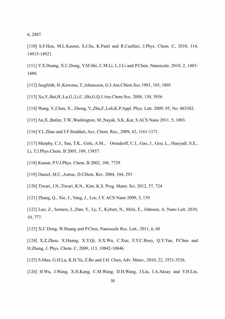
38
6, 2887.
[110] S.F.Hou, M.L.Kasner, S.J.Su, K.Patel and R.Cuellari, J.Phys. Chem. C, 2010, 114,
14915-14921.
[111] Y.X.Huang, X.C.Dong, Y.M.Shi, C.M.Li, L.J.Li and P.Chen, Nanoscale, 2010, 2, 1485-
1488.
[112] Jaegfeldt, H.,Kuwana, T.,Johansson, G.J.Am.CHem.Soc.1983, 105, 1805
[113] Xu,Y.,Bai,H.,Lu,G.,Li,C.,Shi,G.Q.J.Am.Chem.Soc. 2008, 130, 5856
[114] Wang, Y.,Chen, X., Zhong, Y.,Zhu,F.,Loh,K.P.Appl. Phys. Lett. 2009, 95, No. 063302.
[115] An,X.,Butler, T.W.,Washington, M.,Nayak, S.K.,Kar, S.ACS Nano 2011, 5, 1003.
[116] Y.L.Zhao and J.F.Stoddart, Acc. Chem. Res., 2009, 42, 1161-1171.
[117] Murphy, C.J., Sau, T.K., Gole, A.M., Orendorff, C.J., Gao, J., Gou, L., Hunyadi, S.E.,
Li, T.J.Phys.Chem. B 2005, 109, 13857.
[118] Kamat, P.V.J.Phys. Chem. B 2002, 106, 7729
[119] Daniel, M.C.,Astruc, D.CHem. Rev. 2004, 104, 293
[120] Tiwari, J.N.,Tiwari, R.N., Kim, K.S. Prog. Mater. Sci. 2012, 57, 724
[121] Zhang, Q., Xie, J., Yang, J., Lee, J.Y. ACS Nano 2009, 3, 139.
[122] Luo, Z., Somers, L.,Dan, Y., Ly, T., Kybert, N., Mele, E., Johnson, A. Nano Lett. 2010,
10, 777.
[123] X.C.Dong, W.Huang and P.Chen, Nanoscale Res. Lett., 2011, 6, 60
[124] X.Z.Zhou, X.Huang, X.Y.Qi, S.X.Wu, C.Xue, F.Y.C.Boey, Q.Y.Yan, P.Chen and
H.Zhang, J. Phys. Chem. C, 2009, 113, 10842-10846.
[125] S.Mao, G.H.Lu, K.H.Yu, Z.Bo and J.H. Chen, Adv. Mater., 2010, 22, 3521-3526.
[126] H.Wu, J.Wang, X.H.Kang, C.M.Wang, D.H.Wang, J.Liu, I.A.Aksay and Y.H.Lin,

39
Talanta, 2009, 80, 403-406

40
Chapter II
Graphene Preparation and Characterization
Chapter II. Graphene Preparation and Characterization ....................................................................... 41
2.1 Generalities ..................................................................................................................................... 41
2.2 Preparation ...................................................................................................................................... 42
2.2.1 Exfoliated graphene ................................................................................................................ 42
2.2.2 Epitaxial graphene .................................................................................................................. 43
2.2.3 CVD graphene ........................................................................................................................ 44
2.2.3.1 PECVD ........................................................................................................................... 46
2.2.3.2 Transfer of Graphene ...................................................................................................... 46
2.3 Characterization techniques ............................................................................................................ 48
2.3.1 Scanning Electron Microscopy (SEM) ................................................................................... 48
2.3.2 Atomic Force Microscopy (AFM) .......................................................................................... 49
2.3.3 Raman spectroscopy ............................................................................................................... 50
2.3.4 Photoemission spectroscopy (PES)......................................................................................... 51
2.3.4.1 Generalities ..................................................................................................................... 51
2.3.4.2 X-ray Photoelectron Spectroscopy (XPS) ...................................................................... 52
2.3.4.3 Ultraviolet Photoelectron Spectroscopy (UPS) .............................................................. 53
2.3.4.4 Angle-resolved photoemission spectroscopy (ARPES) .................................................. 53
2.3.4.5 Auger electron spectroscopy (AES) ................................................................................ 56
2.3.4.6 Electron energy loss spectroscopy (EELS) ..................................................................... 56
2.4 Conclusions ..................................................................................................................................... 58
Reference .............................................................................................................................................. 60

41
Chapter II. Graphene Preparation and Characterization
2.1 Generalities
Most of the performances of graphene based devices rely on its surface
characteristics. However, required physical properties and the overall quality of the graphene
films differ depending on the various applications. For example, graphene with a highly
crystallized grain and minimized structural defects are favorable for graphene transistor while
some surface defects are usually preferable for gas sensing applications. Hence preparing
appropriate material is of great importance for a certain device application. In this chapter
several commonly used synthesis methods are introduced among which, one method which
was originally developed in LPICM [1].
Once synthesized, it is necessary that graphene films are characterized to understand
its electrical and physical properties for further device applications. There are several well-
known common techniques to characterize physical properties of 2D materials such as
scanning electron microscopy (SEM), transmission electron microscopy (TEM), atomic force
microscopy (AFM), Raman spectroscopy, photoemission spectroscopy (PES), optical
microscopy, optical transmittance and so on.
SEM and AFM are choice techniques for investigating the surface of materials at
nanoscale. They can reveal the morphology and the thickness of the material but it becomes
not clear when the graphene sheet is homogeneous and continuous as we merely find
structural deformations. TEM provides useful information about material crystallinity by
investigating its cross-section. But it requires destructive pre-treatment of the sample and the
measurement is expensive and time consuming. Raman spectroscopy is the most powerful
technique for non-destructively characterizing graphene and a simple measurement brings
fruitful information about graphene, especially about its quality. ARPES is commonly used
for studying material‟s energy dispersion respect to its momentum. Optical microscopy can
be simply used to locate graphene layers by comparing the image contrast and optical
transmittance measurement. It is utilized, for example, for counting the number of layers. In
this chapter we will closely look at some of characterization techniques used for investigating
the properties of graphene used in the experiments.

42
2.2 Preparation
2.2.1 Exfoliated graphene
Structurally graphite allotrope is formed by stacking many layers of graphene sheets. In
principle, each layer of graphite is stacked by week Van-der-Waals force and therefore
graphene can be detached by breaking these bonds. Hence the exfoliation of graphite to
produce graphene has been investigated by various experimental approaches including
mechanical and chemical methods.
Mechanical exfoliation is the process where the best quality graphene, in terms of
structural integrity and electronic performance, can be obtained. In this process, graphene is
separated by peeling off a layer from commercially available Highly Oriented Pyrolytic
Graphite (HOPG) sheet by using scotch tape then transferred onto the substrate. The
schematic diagram of the mechanical exfoliation procedure by using scotch tape is
represented in the Figure 2.1.. Thanks to its excellent quality with simple and easy process,
many fundamental studies have been carried out on mechanically exfoliated graphene since
its first isolation by Manchester group [2]. However, graphene produced in this way has a
limitation in sheet size (~micrometers) and low production yield which are sometimes crucial
drawbacks for device applications.
Figure 2.1. Micromechanical exfoliation of 2D crystals. (a) Adhessive tape is pressed against
a 2D crystal so that the top few layers are attached to the tape (b). (c) The tape with crystals

43
of layered material is pressed against a surface of choice. (d) Upon peeling off, the bottom
layer is left on the substrate [3].
On the other hand, high production yield can be achieved by chemical exfoliation
method (Figure 2.2.). In this process [8], graphite is first soaked in mixtures of sulfuric and
nitric acid. Then the acid molecules penetrate into the graphite to form alternating layers
called graphite intercalate compounds (GICs) that expands the interlayer spacing between
graphene sheets. Rapid evaporation of these GICs at high temperature eventually produces
exfoliated graphene sheets [4-6]. Although chemically exfoliated graphene promises high
production rate, chemical treatment during the process generates structural defects [7] that
may affect the intrinsic electronic properties of graphene as well.
Figure 2.2. Experimental procedure for preparation of graphene by liquid phase intercalation
and exfoliation of graphite [8].
2.2.2 Epitaxial graphene
Graphene can also be epitaxially grown. In this case, the graphene layer is obtained by
decomposing the hexagonal single crystal silicon carbide (SiC) surface layers to graphene at
high temperature [9] as illustrated in the Figure 2.3.. On the {0001} surfaces of the hexagonal
SiC single crystal, there are both Si-terminated (0001) and C-terminated (000 ̅) faces. Si-
terminated face is usually preferable for obtaining better homogeneous graphene growth.
Furthermore, a carbon buffer layer is produced through the epitaxial graphene growth on the
Si-face which is electrically inert [10,11].

44
Figure 2.3. Basics of graphene growth by thermal decomposition of SiC, together with the
structural model of bilayer graphene on SiC. Shown as the blue broken line is the buffer layer
[12].
The epitaxial grown graphene on SiC has the primary advantage that it does not require
transfer process since SiC itself serves as a good insulator. Graphene directly grown on
insulating substrate becomes compatible with the Si-based standard microelectronic
technologies for large integrated circuits with dense transistors [13].
In 2007, Zhou et al. reported an interesting characteristic of graphene epitaxially grown
on SiC substrate. In that case, the graphene-substrate interaction caused a band gap opening
of up to ~0.26eV with less than 4 layers [14]. This band gap enables graphene to be useful as
an electronic material especially for field effect transistors (FETs). However, because of the
process complexity difficulties such as determining the face and edge-termination (silicon or
carbon) of the substrate and controlling the decomposition rate, precise control of growth
conditions for graphene on SiC substrate remain up to day a very important challenges.
2.2.3 CVD graphene
Single or few layer graphene can also be synthesized on the surface of transition metal
(e.g., nickel, copper, cobalt, palladium) substrates by chemical vapor deposition (CVD)
process. In this process, carbon-containing gases, usually methane (CH4), are used as
precursors. At high temperature (e.g., at ~1000 ˚C for Ni), compared with room temperature,
relatively large amount of carbon atoms can be dissolved into catalyst metal. Then during the
cooling step, excessive dissolved carbon atoms will diffuse out to the surface of metal

45
substrate which results in graphene layers by surface segregation of carbon [15]. On the other
hand, generally, higher quality of single layer graphene is expected to be grown on the Cu
substate rather than Ni substrate because of its larger grain size with low carbon solubility
compared with Ni subsrate [16]. Low carbon solubility of Cu (0.001~0.008 wt.& at 1,084 ˚C
[17]) allows only the surface reaction with gases thus a single graphene (SLG) layer is
formed by self-limiting mechanism on the substrate. Brief illustration of the CVD process
with Cu substrate [17] is represented in Figure 2.4..
Figure 2.4. Schematic illustration of three main stages of CVD process for graphene growth:
(a) copper foil with native oxide; (b) the exposure of the copper foil to CH4/H2 atmosphere at
1000 ˚C leading to the nucleation of graphene islands; (c) enlargement of the graphene flakes
with different lattice orientations [17].
Depending on various process conditions such as temperature, gas flow rate, metal
substrate and cooling rate, the quality and the properties of synthesized graphene vary
significantly. For example, SLG is usually synthesized on Cu substrate because of its self-
limiting characteristic where the growth stops after one graphene layer is formed at the
surface [16]. The Figure 2.5. shows the Raman spectra of graphene synthesized on Ni
substrate with different cooling rates studied by Qungkai Yu et al. [18]. They investigated
three different cooling rates corresponding to fast (20 ˚C/s), medium (10 ˚C/s) and slow (0.1
˚C/s). The result shows that the optimized cooling rate exists for obtaining better quality
graphene by CVD process where the medium cooling rate is the case for their study.

46
Figure 2.5. Raman spectra of CVD graphene on Ni substrate depending on different cooling
rate [18].
2.2.3.1 PECVD
Thanks to its process advantages, especially possible large area and low-cost
production, CVD process for graphene synthesis is actively studied by many researchers.
However, high process temperature near 1,000 ˚C is a critical issue in terms of industrial
aspects. Hence, like for CNTs, there have been many efforts to lower the process temperature
by employing plasma enhanced CVD (PECVD) process. The process temperature has been
lowered to around 500 ˚C. Many groups are still working on it to optimize and simplify the
process conditions and steps with the improvement of graphene quality [19-21].
2.2.3.2 Transfer of Graphene
Even though large area graphene layers can be grown by CVD process, they are still
on the catalytic metal substrate surface. Once graphene is synthesized on this metal substrate,
it is supposed to be transferred onto the final insulating substrate required for most of
electronic device applications. The Figure 2.6. [22] shows the typical procedures of this
transfer technique. Graphene synthesized by CVD process on Cu metal layer is covered by a

47
sacrificial polymethyl methacrylate (PMMA) and annealed at first. Cu layer is subsequently
removed by wet etching and the remaining graphene attached to the PMMA is rinsed by
deionized (DI) water. Then it is put together onto the target insulating substrate and
subsequently annealed. Finally, PMMA is selectively removed by acetone and only graphene
remains on the insulating substrate [22-24].
Figure 2.6. Transfer of graphene [22]
However, this transfer process has many drawbacks such as surface contamination
originating from PMMA [23,24], morphological and structural deformation (e.g., wrinkles,
cracks, defects) of graphene layer [25] and it is even quite sophisticated process that requires
appreciable time and cost [26]. For these reasons, direct growth of graphene on insulating
substrate is desirable in terms of device applications for many researchers. LPICM, by using
home-made triode type PECVD system, could directly grow graphene on the insulating
substrates. This will be explained in detail in Chapter 3.

48
2.3 Characterization techniques
2.3.1 Scanning Electron Microscopy (SEM)
Scanning electron microscopy is one of simple and fast techniques to verifying the
quality of the graphene on the substrate. It is a non-destructive technique so that the
characterized graphene can later be used for device applications. The image taken by SEM
provides useful information especially for polycrystalline graphene such as its location on the
substrate, grain boundaries and structural deformations including wrinkles, vacancies, cracks,
and so on.
The principle of this technique lies on the interpretation of secondary electrons
generated by the interaction between incident electrons and the target sample. Incident
electrons are significantly scattered and therefore, SEM operates in two different modes
depending on the scattering type: elastic or inelastic.
First mode, based on the electron inelastic scattering, is the most commonly used
way to investigate the surface morphology. SEM collects low-energy secondary electrons
coming from the k-orbitals of only few atomic layers [27-29]. Second mode employs the
electron elastic scattering where the electrons undergo no energy loss which is called back
scattered electron imaging. SEM collects high-energy secondary electrons coming from the
nuclei of bulk atoms. This enables us to have an image contrast as a function of elemental
composition which is for investigating the existing elements but not for surface morphology.
The Figure 2.7. is an example of SEM image for graphene-supported Pt nanoparticles taken
as both modes [30]. A typical low-energy secondary electron image is represented in the
Figure 2.7.(a) and a corresponding back scattered electron image on the same spot is
demonstrated in the Figure 2.7.(b). In the Figure 2.7.(b), Pt nanoparticles are highlighted by
brighter regions which are not clearly observable in the low-energy secondary electron image
(Figure 2.7.(a)).
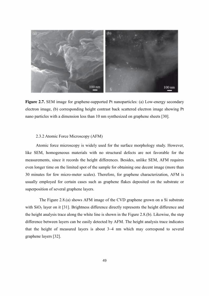
49
Figure 2.7. SEM image for graphene-supported Pt nanoparticles: (a) Low-energy secondary
electron image, (b) corresponding height contrast back scattered electron image showing Pt
nano particles with a dimension less than 10 nm synthesized on graphene sheets [30].
2.3.2 Atomic Force Microscopy (AFM)
Atomic force microscopy is widely used for the surface morphology study. However,
like SEM, homogeneous materials with no structural defects are not favorable for the
measurements, since it records the height differences. Besides, unlike SEM, AFM requires
even longer time on the limited spot of the sample for obtaining one decent image (more than
30 minutes for few micro-meter scales). Therefore, for graphene characterization, AFM is
usually employed for certain cases such as graphene flakes deposited on the substrate or
superposition of several graphene layers.
The Figure 2.8.(a) shows AFM image of the CVD graphene grown on a Si substrate
with SiO2 layer on it [31]. Brightness difference directly represents the height difference and
the height analysis trace along the white line is shown in the Figure 2.8.(b). Likewise, the step
difference between layers can be easily detected by AFM. The height analysis trace indicates
that the height of measured layers is about 3~4 nm which may correspond to several
graphene layers [32].
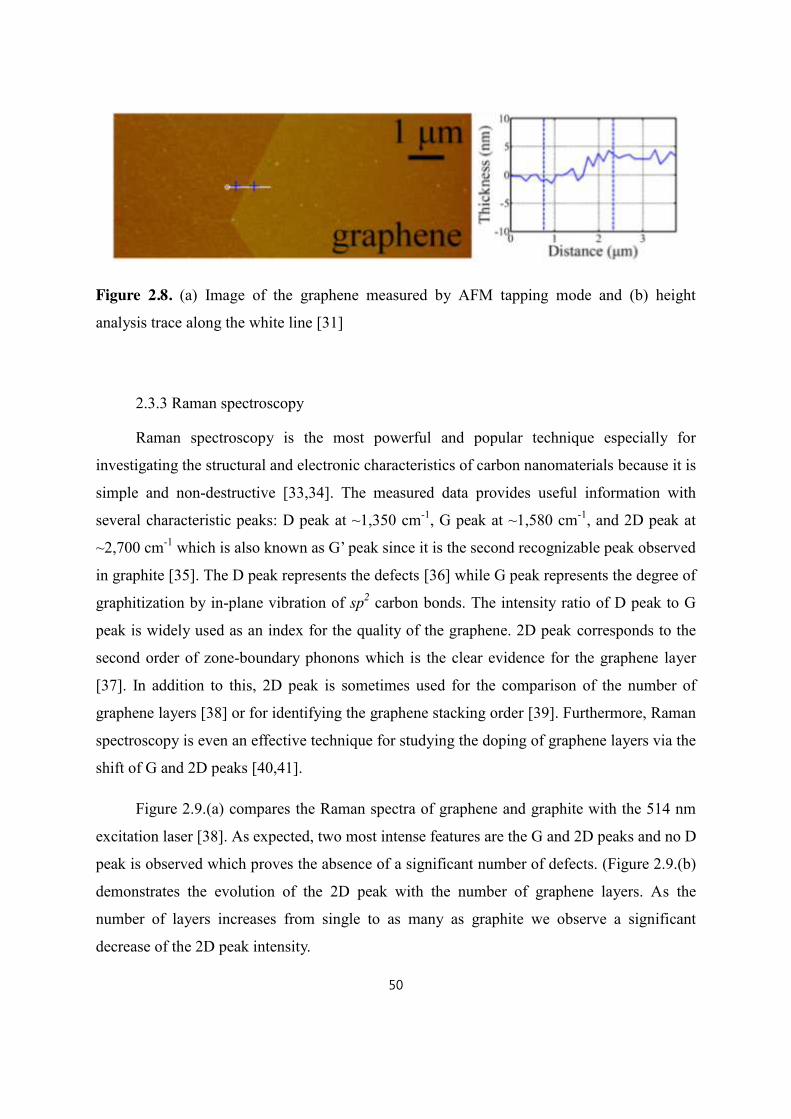
50
Figure 2.8. (a) Image of the graphene measured by AFM tapping mode and (b) height
analysis trace along the white line [31]
2.3.3 Raman spectroscopy
Raman spectroscopy is the most powerful and popular technique especially for
investigating the structural and electronic characteristics of carbon nanomaterials because it is
simple and non-destructive [33,34]. The measured data provides useful information with
several characteristic peaks: D peak at ~1,350 cm-1, G peak at ~1,580 cm-1, and 2D peak at
~2,700 cm-1 which is also known as G‟ peak since it is the second recognizable peak observed
in graphite [35]. The D peak represents the defects [36] while G peak represents the degree of
graphitization by in-plane vibration of sp2 carbon bonds. The intensity ratio of D peak to G
peak is widely used as an index for the quality of the graphene. 2D peak corresponds to the
second order of zone-boundary phonons which is the clear evidence for the graphene layer
[37]. In addition to this, 2D peak is sometimes used for the comparison of the number of
graphene layers [38] or for identifying the graphene stacking order [39]. Furthermore, Raman
spectroscopy is even an effective technique for studying the doping of graphene layers via the
shift of G and 2D peaks [40,41].
Figure 2.9.(a) compares the Raman spectra of graphene and graphite with the 514 nm
excitation laser [38]. As expected, two most intense features are the G and 2D peaks and no D
peak is observed which proves the absence of a significant number of defects. (Figure 2.9.(b)
demonstrates the evolution of the 2D peak with the number of graphene layers. As the
number of layers increases from single to as many as graphite we observe a significant
decrease of the 2D peak intensity.

51
Figure 2.9. Raman spectra with the 514 nm excitation laser: (a) Comparison of graphite and
graphene, (b) Evolution of the spectra with the number of layers [38].
2.3.4 Photoemission spectroscopy (PES)
2.3.4.1 Generalities
Photoemission spectroscopy (PES), in general, refers to energy measurement of
electrons emitted by the photoelectric effect, in order to determine the binding energies of
electrons in a substance. It has been established as one of the most important techniques to
study the electronic structure of molecules, solids and surfaces [42,43]. Quasi-
monochromatic light sources are used for PES and depending on its energy the inspection
region in terms of energy varies. For example, ultraviolet photoemission (UPS) which is
mainly for the angle-resolved investigation of valence band states (ARUPS), uses the light
source that has photon energy of about 10-50 eV often produced by discharge lamps with rare
gases like helium (HeI : 21.23 eV, HeII :40.82 eV). On the other hand, aluminum (Al-K 1,2:
1486.6 eV) and magnesium (Mg-K 1,2: 1253.6 eV) anodes are often used for X-ray
photoemission spectroscopy (XPS) to investigate the core-level states at higher binding
energies [44-47].
The principle of a modern photoemission spectrometer is represented in the Figure

52
2.10.(a). Monochromatic photons with energy hv produced by a light source are directed on
the sample surface. Then the kinetic energy Ekin of the photoelectrons and the acceptance
angle 𝜃 and other parameters are recorded by electrostatic analysers. Figure 2.10.(b)
describes the photoemission process in the single-particle picture. We see that the electrons
with binding energy EB are excited above the vacuum level Evac with the incident photon
energy higher than the sum of binding energy and work function. The photoelectron
distribution I(Ekin) can be measured by counting emitted electrons and can be reproduced as
an image of occupied density of electronic states N(EB) [48].
Figure 2.10. (a) Principle of a modern photoemission spectrometer. (b) Schematic view of
the photoemission process in the single-particle picture [36].
2.3.4.2 X-ray Photoelectron Spectroscopy (XPS)
XPS is the most widely used surface analysis technique because of its simplicity in
use and data interpretation. It is also known as Electron Spectroscopy for Chemical Analysis
(ESCA) since the elements composition on the sample surface can be analyzed by this
technique. XPS uses soft x-rays with a photon energy of 200~2,000 eV as a source of exciting
radiation while aluminum (Al-K 1,2: 1486.6 eV) and magnesium (Mg-K 1,2: 1253.6 eV)
anodes are the most commonly used sources [44-47]. There is a characteristic binding energy
for every element associated with each core atomic orbital. Thus the presence of peaks at

53
particular energies indicates the presence of a specific element. The intensity of the peaks is
related to the concentration of the element such that the quantitative analysis of the elements
composition on the sample surface can also be carried out.
2.3.4.3 Ultraviolet Photoelectron Spectroscopy (UPS)
UPS generally uses the light source that has photon energy of about 10-50 eV. The
helium (HeI : 21.23 eV, HeII :40.82 eV) gas discharge lamp is the most commonly used
source [44-47]. Unlike XPS, such low energy source is only capable of ionizing electrons
from the outermost levels of atoms correspond to the valence levels, but it measures them
with better accurately [48]. With HeI (21.23 eV) source Turner‟s group obtained an energy
resolution of up to 0.02 eV. In addition, angle-resolved measurement of UPS enables
understanding of the complete band structure in k-space.
2.3.4.4 Angle-resolved photoemission spectroscopy (ARPES)
Figure 2.11. shows a typical experimental photoemission process for the ARPES
measurement system. Monochromatic laser having energy hv is incident on the sample and
the detector detects electrons coming from the sample by the photoemission process. The
kinetic energy and the emission angle of the electrons are then recorded at the same time.

54
Figure 2.11. Schematic diagram of photoemission process on the sample surface
This photoemission process is commonly explained by the three-step model [49] :
(i) Optical excitation of the bulk electron
(ii) Travel of the excited electron to the surface
(iii) Emission of the photoelectron under vacuum
For the first step, the monochromatic laser with energy hv, excites the electron from an
occupied state to an unoccupied state. On the second step, this excited electron travels to the
surface with the probability concerning its mean free path. Electrons undergoes inelastic
scattering during this travel would finally be recorded as a continuous background of the
photoemission spectra. Once the electron reaches the surface having enough energy to
overcome the work function of the material, for the last step, it is emitted to the vacuum so
that the corresponding photoemission spectra are recorded.
Experimentally, the kinetic energy of the photoelectrons with their polar (θ) and
azimuthal (φ) emission angles represented in the Figure 2.11. are the three main quantities
measured in a photoemission experiment.

55
Figure 2.12. shows a simplified image for explaining the energy conservation law in
the photoemission process where the measured kinetic energy of the emitted electrons can be
simply related to incident light energy by
| | (5)
denotes the electron kinetic energy and is the energy of the incident light.
stands for the work function of the material that is the minimum energy required for electrons
to escape from Fermi level to the vacuum while corresponds to the binding energy of the
electron.
Figure 2.12. Incident X-ray energy and kinetic energy of emitted electrons
Through the photoemission process explained by the three-step model with such
energy conservation, the momentum parallel to the surface is also conserved. The emitted
electron momentum can be described as:
√ 𝜃 (6)

56
where and are the momentum and the wave vector parallel to the surface respectively.
The lattice constant of graphene, or 2.45 Å, gives the first Brillouin zone boundary of 2.56 Å -
1 while the wave vector of the photon corresponding to 50 eV is about 0.025 Å -1. This value
is less than 1% of the first BZ, hence the photon momentum with its energy lower than 50 eV
is almost negligible.
In our measurement, the kinetic energy of photo electrons and corresponding
intensity were recorded with varying analyser acceptance angle, 𝜃. was fixed for the
whole measurement and therefore parallel wave vector could have been directly deduced
from √ 𝜃. Binding energy, could also be simply calculated from
| |. Finally, the result of our measurement is expressed by a two-variable
photocurrent function I( , ).
2.3.4.5 Auger electron spectroscopy (AES)
Auger electron spectroscopy (AES) is another PES technique based on Auger effect.
The Auger effect is an electronic process resulting from the electron transitions in an excited
atom. In an atom, excited by the light source with energies in the range of several eV to 50
keV, a core level electron can be removed leaving behind a hole resulting in an unstable state.
As an outer shell electron fills the core hole, it loses an amount of energy equal to the orbital
energy difference. The transition energy can be coupled to a second outer shell electron,
which will be emitted from the atom if the transferred energy is greater than the orbital
binding energy. [50-55] An emitted electron has a kinetic energy of:
(7)
where ECore, E1OS, E2OS are the core level, first outer shell, and second outer shell elctron
binding energies respectively.
2.3.4.6 Electron energy loss spectroscopy (EELS)
Like above stated other PES techniques, in electron energy loss spectroscopy (EELS)
a sample is exposed to a beam of electrons with a known, narrow range of kinetic energies.

57
Most of the incident electrons undergo elastic scattering while some of them will undergo
inelastic scattering. Inelastic interactions can happen via various way including phonon
excitations, inter and intra band transitions, plasmon excitations, inner shell ionizations, and
so on. Electrons undergone such inelastic scattering are slightly and randomly deflected from
the incident direction and lose that much of energy. The amount of such energy loss can be
measured by an electron spectrometer. EELS analysis is based on the interpretation of this
measured energy loss
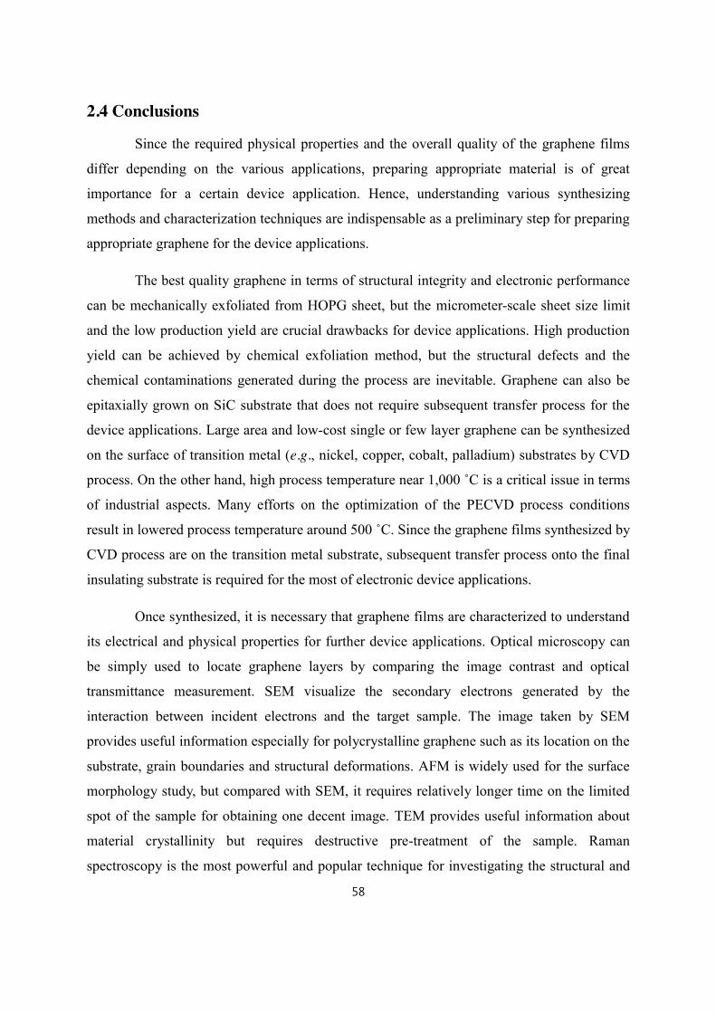
58
2.4 Conclusions
Since the required physical properties and the overall quality of the graphene films
differ depending on the various applications, preparing appropriate material is of great
importance for a certain device application. Hence, understanding various synthesizing
methods and characterization techniques are indispensable as a preliminary step for preparing
appropriate graphene for the device applications.
The best quality graphene in terms of structural integrity and electronic performance
can be mechanically exfoliated from HOPG sheet, but the micrometer-scale sheet size limit
and the low production yield are crucial drawbacks for device applications. High production
yield can be achieved by chemical exfoliation method, but the structural defects and the
chemical contaminations generated during the process are inevitable. Graphene can also be
epitaxially grown on SiC substrate that does not require subsequent transfer process for the
device applications. Large area and low-cost single or few layer graphene can be synthesized
on the surface of transition metal (e.g., nickel, copper, cobalt, palladium) substrates by CVD
process. On the other hand, high process temperature near 1,000 ˚C is a critical issue in terms
of industrial aspects. Many efforts on the optimization of the PECVD process conditions
result in lowered process temperature around 500 ˚C. Since the graphene films synthesized by
CVD process are on the transition metal substrate, subsequent transfer process onto the final
insulating substrate is required for the most of electronic device applications.
Once synthesized, it is necessary that graphene films are characterized to understand
its electrical and physical properties for further device applications. Optical microscopy can
be simply used to locate graphene layers by comparing the image contrast and optical
transmittance measurement. SEM visualize the secondary electrons generated by the
interaction between incident electrons and the target sample. The image taken by SEM
provides useful information especially for polycrystalline graphene such as its location on the
substrate, grain boundaries and structural deformations. AFM is widely used for the surface
morphology study, but compared with SEM, it requires relatively longer time on the limited
spot of the sample for obtaining one decent image. TEM provides useful information about
material crystallinity but requires destructive pre-treatment of the sample. Raman
spectroscopy is the most powerful and popular technique for investigating the structural and

59
electronic characteristics of carbon nanomaterials because it is simple and non-destructive.
Generally, three major peaks are employed for characterizing graphene quality: D peak at
~1,350 cm-1, G peak at ~1,580 cm-1, and 2D peak at ~2,700 cm-1. PES techniques including
XPS, UPS, ARPES, AES and EELS are extensively used as the important techniques to study
the electronic structure and chemical compositions of molecules, solids and surfaces.

60
Reference
[1] C.S.Lee, C.S.Costel, W.Moujahid, B.Lebental, M.Chaigneau, M.Châtelet, F.L.Normand
and J.L.Maurice, Syntehsis of conducting transparent few-layer graphene directly on glass at
450 C, Nanotechnolgoy, 23 (2012) 265603
[2] Novoselov, K.S., Gaim, A.K., Morozov, S.V., Jian, D., Zhang, Y., Dubonos, S.V.,
Grigorieva, I.V. and Firsov, A.A. Electric field effect in atomically thin carbon films. Science
306, 666-669 (2004)
[3] K S Novoselov and A H Castro Neto, Two-dimensional crystals-based heterostructures:
materials with tailored properties, Phys.Scr.T146 (2012) 014006
[4] G.Eda, C.Mattevi, H.Yamaguchi, H.Kim, M.Chhowalla, Insulator to semi-metal transition
in graphene oxide, Journal of Physical Chemistry C 133(2009) 15768-15771.
[5] M.Lotya, Y.Hernadez, P.J.King, R.J.Smith, V.Nicolosi, L.S.Karlsson, F.M.Blighe,
S.De,Z.Wang, I.T.McGovern, G.S.Duesberg, J.N.Coleman, Liquid phase production of
graphene by exfoliation of graphite in surfactant/water solutions, Journal of American
Chemical Society 131 (2009) 3611-3620.
[6] C.Nethravathi, M.Rjamathi, Chemically modified graphene sheets produced by the
solvothermal reduction of colloidal dispersions of graphite oxide, Carbon 46 (2008) 1994-
1998
[7] V.Singh, D.Joung, L.Zhai, S.Das, S.I.Khondaker, S.Seal, Graphene based materials: Past,
present and future, Progress in Materials Science 56 (2011) 1178-1271
[8] Ming Zhou, Tian Tian, Xuanfu Li, Xudong Sun, Juan Zhang, Ping Cui, Jie Tang, and Lu-
Chang Qin, Production of Graphene by Liquid-Phase Exfoliation of Intercalted Graphite
[9] J.Hass, W.A.de Heer and E.H.Conrad, J.Phys.: Condens., The growth and morphology of
epitaxial multilayer graphene, Matter, 2008, 20, 323202.
[10] A. Mattausch and O. Pankratov, Ab initio study of graphene on SiC,Phys. Rev. Lett.,
2007, 99, 076802.
61
[11] F.Varchon, R.Feng, J.Hass, X.Li, B.NgocNguyen, C.Naud, P.Mallet, J.-Y. Veuille,
C.Berger, E.H.Conrad and L.Magaud, Electronic structure of epitaxial graphene layers on
SiC: effect of the substrate,Phys. Rev. Lett., 2007, 99, 126805
[12] Wataru Norimatsu and Michiko Kusunoki, Epitaxial graphene on SiC{0001}: advances
and perspectives, Phys. Chem. CHem. Phys., 2014, 16, 3501-3511.
[13] J.Kedzierski, P.L.Hsu, P.Healey, P.W.Wyatt, C.L.Keast, M.Sprinkle, C.Berger and
W.A.de Heer, Epitaxial graphene transistors on SiC substrates, IEEE Trans. Electron Devices,
2008, 55, 2078-2085.
[14] S.Y.Zhou, G.H.Gweon, A.V.Fedorov, P.N.First, W.A. de Heer, D.H.Lee, F.Guinea,
A.H.Castro Nto and A.Lanzara, Substrate-induced bandgap opening in epitaxial graphene,Nat.
Mater., 2007, 6, 770-775.
[15] J.Wintterlin, M.L.Bocquet, Graphene on metal surfaces, Surface Science 603 (2009)
1841-1852
[16] Xuesong Li, Weiwei Cai, Jinho An, Seyoung Kim, Junghyo Nah, Dongxing Yang,
Richard Piner, Aruna Velamakanni, Inhwa Jung, Emanuel Tutuc, Sanjay K. Banerjee, Luigi
Colombo, Rodney S. Ruoff, Large-Area Synthesis of High-Quality and Uniform Graphene
Films on Copper Foils,Science, 2009, 325, 1312-1314.
[17] Cecilia Mattevi, Hokwon Kim and Manish Chhowalla, A review of chemical vapour
deposition of graphene on copper, J. Mater. Chem., 2011, 21, 3324-3334
[18] Yu, Q., Lian, J., Siriponglert, S., Li,H., Chen, Y.P. and Pei, S.-S. Graphene segregated on
Ni surfaces and transferred to insulators. Applied Physics Letters 93, 113103-3 (2008).
[19] Yuan, G.D., Zhang, W.J., Yang, Y., Tang, Y.B., Li, Y.Q., Wang, J.X., Meng, X.M., He,
Z.B., Wu, C.M.L., Bello, I., Lee, C.S. and Lee, S.T. Graphene sheets via microwave chemical
vapor deposition. Chemical Physics Letters 467, 361-364 (2009)
[20] J.L. Qia, W.T. Zheng, X.H. Zheng, X. Wang, H.W. Tian, Relatively low temperature
synthesis of graphene by radio frequency plasma enhanced chemical vapor deposition.,
Applied Surface Science 257 (2011) 6531–6534

62
[21] Sunny Chugh, Ruchit Mehta, Ning Lu, Francis D. Dios, Moon J. Kim, Zhihong Chen,
Comparison of graphene growth on arbitrary non-catalytic substrates using low-temperature
PECVD., CARBON 93 (2015) 393–399
[22] Yuanyuan Han, Lei Zhang, Xiujuan Zhang, Kaiqun Ruan, Linsong Cui, Yuming Wang,
Liangsheng Liao, Zhaokui Wang and Jiansheng Jie, Clean surface transfer of graphene films
via an effective sandwich method for organic light- emitting diode applications., J. Mater.
Chem. C, 2014, 2, 201–207
[23] Xuesong Li, Yanwu Zhu, Weiwei Cai, Mark Borysiak, Boyang Han, David Chen,
Richard D. Piner, Luigi Colombo, and Rodney S. Ruoff, Transfer of Large-Area Graphene
Films for High-Performance Transparent Conductive Electrodes., Nano Lett., Vol. 9, No. 12,
2009
[24] Xuelei Liang, Brent A. Sperling, Irene Calizo, Guangjun Cheng, Christina Ann Hacker,
Qin Zhang, Yaw Obeng, Kai Yan, Hailin Peng, Qiliang Li, Xiaoxiao Zhu, Hui Yuan, Angela
R. Hight Walker, Zhongfan Liu, Lian-mao Peng, and Curt A. Richter, Toward Clean and
Crackless Transfer of Graphene., vol. 5 no. 11, 9144–9153, 2011
[23] Ishigami, M.,Chen,J.H., Cullen, W.G., Fuhrer, M.S. and Williams, E.D., Atomic
Structure of Graphene on SiO2., Nano Letters 7, 1643-1648
[24] Pirke, A., Chan, J., Venugopal, A., Hinojos, D., Magnuson, C.W., McDonnell, S.,
Colombo, L.,Vogel, E.M., Ruoff, R.S. and Wallace, R.M. The effect of chemical residues on
the physical and electrical properties of chemical vapor deposited graphene transferred to
SiO2. Applied Physics Letters 99, 122108-3 (2011)
[25] Lin, Y.-C., Jin, C., Lee, J.-C., Jen, S.-F., Suenaga, K. and Chiu, P.-W. Clean Transfer of
Graphene for Isolation and Suspension. ACS Nano 5, 2362-2368 (2011)
[26] Liang, X., Sperling, B.A., Calizo, I., Cheng, G., Hacker, C.A., Zhang, Q., Obeng, Y., Yan,
K., Peng, H., Li, Q., Zhu, X., Yuan, H., Hight Walker, A.R., Liu, Z., Peng, L.-m. and Rchter,
C.A. Toward Clean and Crackless Transfer of Graphene. ACS Nano 5, 9144-9153 (2011)
[27] Seiler, H. Secondary electron emission in the scanning electron microscope. Journal of

63
Applied Physics 54,R1-R18 (1983).
[28] Park, M.-H., Kim, T.-H. and Yang, C.-W. Thickness contrast of few-layered graphene in
SEM. Surface and Interface Analysis, n/a-n/a (2012)
[29] Kochat, V., Pal, A.N., Sneha, E.S., Sampathkumar, A., Gairola, A., Shivashankar, S.A.,
Raghavan, S. and Ghosh, A.High contrast imaging and thickness determination of graphene
with in-column secondary electron microscopy. Journal of Applied Physics 110, 014315-5
(2011)
[30] Lifeng Dong, Raghavendar Reddy Sanganna Gari, Zhou Li, Michael M. Craig, Shifeng
Hou, Graphene-supported platinum and platinum-ruthenium nanoparticles with high
electrocatalytic activity for methanol and ethanol oxidation, carbon, 48, (2010), 781-787
[31] Shuangxi Xie, Niadong Jiao, Steve Tung, and Lianqing Liu, Fabrication of SWCNT-
Graphene Field-Effect Transistors, Micromachines 2015, 6(9), 1317-1330
[32] K. S. Novoselov, A. K. Geim, S. V. Morozov, D. Jiang, Y. Zhang, S. V. Dubonos, I. V.
Grigorieva, A. A. Firsov, Electric Field Effect in Atomically Thin Carbon Films, Science,
2004, Vol. 306. pp.666-669.
[33] Ferrari, A.C. and Robertson, J.Interpretation of Raman spectra of disordered and
amorphous carbon. Physical Review B 61, 14095-14107 (2000)
[34] Ferrari, A.C. and Robertson, J. Resonant Raman spectroscopy of disordered, amorphous,
and diamond like carbon. Physical Review B 64, 075414 (2001)
[35] R.P.Vidano and D. B. Fischbach, OBSERVATIONOF RAMANBAND SHIFTING
WITH EXCiTATION WAVELENGTH FOR CARBONS AND GRAPHITES, Solid State
Commun. Vol. 39, pp.341-344 (1981)
[36] F.Tuinstra and J.Kenig, Raman Spectrum of Graphite, J.Chem. Phys. 53, 1126 (1970)
[37] R.J.Nemanich and S.A. Solin, First-and second-order Raman scattering from finite-size
crystals of graphite, Phys. Rev. B 20, 392 (1979)
[38] A.C.Ferrari, J.C.Meyer, V.Scardaci, C.Casiraghi, M.Lazzeri, F.Mauri, S.Piscanec,

64
D.Jiang, K.S.Novoselov, S.Roth, and A.K.Geim, Raman Spectrum of Graphene and
Graphene layers, Phy.Rev.Lett. 97, 187401 (2006)
[39] Andrea C.Ferrari and Denis M. Basko, Raman spectroscopy as a versatile tool for
studying the properties of graphene, Nature nanotechnology, vol8. April 2013
[40] Pisana, S., Lazzeri, M., Casiraghi, C., Novoselov, K.S., Geim, A.K., Ferrari, A.C. and
Mauri, F. Breakdown of the adiabatic Born-Oppenheimer approximation in graphene. Nat
Mater 6, 198-201 (2007)
[41] DasA, PisanaS, ChakrabortyB, PiscanecS, Saha, S.K., Waghmare, U.B., Novoselov, K.S.,
Krishnamurthy, H.R., Geim, A.K., Ferrari, A.C. and Sood, A.K. Monitoring dopants by
Raman scattering in an electrochemically top-gated graphene transistor. Nat. nanotechnol. 3,
210-215 (2008)
[42] Cardona M and Ley L(eds) 1978 Photoemission in Solids I (Topics in Applied Physics
vol 26)(Berlin: Springer)
[43] Hufner S 2003 Photoelectron Spectroscopy. Principles and Applications 3rd edn (Berlin:
Springer)
[44] Friedrich Reinert and Stefan Hufner, Photoemeission spectroscopy-from early days to
recent applications, New Journal of Physics 7 (2005) 97
[45] Turner D W, Baker C, A D and Brundle C R, Molecular Photoelectron Spectroscopy,
Phil. Trans. Ray. Soc. Land. A. 268, 7-31 (1970)
[46] D. W. Turner and M. I. Al Jobory, Determination of ionization potentials by
photoelectron energy measurement, The Journal of Chemical Physics. Vol. 37, No. 12,
3007-8. (1962)
[47] Nordling C, Sokolowski E and Siegbahn K, Precision method for obtaining absolute
values of atomic binding energies, Phys. Rev. 105 1676-7. (1957)
[48] Baker A.D. and Betteridge D., Photoelectron Spectroscopy. Chemical and Analytical
Aspects, Pergamon Press, 1972 p.ix

65
[49] W.Spieer, Photoemissive, photoconductive, and optical absorption studies of alkali-
antimony compounds, Phys. Rev. 112, 114 (1958)
[50] Thomas A., Carlson, Photoelectron and Auger Spectroscopy, New York: Plenum Press.
ISBN 0-306-33901-3. (1975)
[51] Briggs, David; Martin P. Seah, Practical Surface Analysis by Auger and X-ray
Photoelectron Spectroscopy, Chichester: John Wiley & Sons. ISBN 0-471-26279-X. (1983).
[52] Thompson, Michael; M. D. Baker; A. Christie; J. F. Tyson, Auger Electron Spectroscopy,
Chichester: John Wiley & Sons. ISBN 0-471-04377-X. (1985).
[53] Davis, L. E. (ed.), Modern Surface Analysis: Metallurgical Applications of Auger
Electron Spectroscopy (AES) and X-ray Photoelectron Spectroscopy (XPS), Warrendale: The
Metallurgical Society of AIME. ISBN 0-89520-358-8. (1980).
[54] Feldman, Leonard C.; James W. Mayer, Fundamentals of Surface and Thin Film
Analysis, Upper Saddle River: Prentice Hall. ISBN 0-13-500570-1. (1986).
[55] Oura, K., V. G. Lifshits, A. A. Saranin, A. V. Zotov, M. Katayama., Surface Science: An
Introduction.,Berlin: Springer. ISBN 3-540-00545-5. (2003)

66
Chapter III
Prepared Graphene
Chapter III. Prepared Graphene ............................................................................................................ 67
3.1 Prepared graphene ........................................................................................................................... 67
3.1.1 PECVD interfacial graphene growth (LPICM) ...................................................................... 68
3.1.2 Epitaxial graphene (LPN) ....................................................................................................... 70
3.2 Graphene Characterization .............................................................................................................. 71
3.3 Conclusions ..................................................................................................................................... 73
Reference .............................................................................................................................................. 74

67
Chapter III. Prepared Graphene
3.1 Prepared graphene
In this chapter, we briefly describe the preparation of the graphene samples that were
further investigated in thesis and give some of the characterization results. The different types
of graphene samples are summarized in the Figure 3.1.. The LPICM graphene is synthesized
by interfacial PECVD technique [1]. We used two of the samples from other labs: one is from
Laboratoire de Photonique et Nannostructures (LPN) prepared by epitaxial growth [2] and the
other is from Thales R&T synthesized by CVD and transferred to Si wafer. At the same time,
commercial graphene samples are also used where all the graphene layers are synthesized by
conventional CVD process and transferred either to glass or Si wafer substrates with 285 nm
of SiO2 layer on it [3-5]. In what follows, since the conventional CVD process can explain
well the growth process of commercial graphene and the graphene from Thales [3-5], we
simply describe the process of the PECVD interfacial graphene from LPICM and that of the
epitaxial graphene from LPN.
Figure 3.1. Graphene samples prepared in various ways for this thesis

68
3.1.1 PECVD interfacial graphene growth (LPICM)
Except epitaxially synthesized graphene on SiC substrate, most of growth techniques
essentially require metal substrate to decompose hydrocarbon gas and to conduct low
temperature crystallization of carbon atoms. Once graphene is synthesized on such metal
substrate, it is supposed to be transferred onto another insulating substrate for most of
electronic device applications. For example, for CVD graphene, usually the synthesized layer
is covered by polymethyl methacrylate (PMMA) and detached together from metal substrate
to be transferred onto insulating substrate (see < 2.2.3.2 Transfer of Graphene > for further
details).
However, this transfer process has many drawbacks such as surface contamination
originating from PMMA [6,7], structural deformation (e.g., wrinkles, cracks, defects) of
graphene layer [8] and it is even quite sophisticated process that requires appreciable time
and cost [9]. For these reasons, direct growth of graphene on insulating substrate is desirable
in terms of device applications for many researchers.
In LPICM, by using home-made triode type PECVD system we could directly grow
graphene on the insulating substrates such as silicon wafer covered with SiO2, and glass.
Figure 3.2. shows a schematic diagram of the PECVD system.
Figure 3.2. Schematic diagram of triode type PECVD system at LPICM

69
Firstly, the substrate is chemically cleaned by piranha solution (H2SO4:H2O2 = 3:1), a
mixture of sulfuric acid (Sigma Aldrich, 339741, 99.9%) and hydrogen peroxide for 30
minutes at 150 ˚C. After being rinsed by deionized (DI) water, it was dried by nitrogen and
placed in the home-made evaporator chamber. Before the metal evaporation, substrate was
again cleaned by Ar plasma. Then 200 nm of Ni thin film is directly deposited on the
substrate under ultra high vacuum (UHV) conditions by e-beam evaporation. Prepared metal
substrate is subsequently transferred to the PECVD system and is placed on the cathode
substrate holder made of graphite. The system is then pumped out to its base pressure of
~2x10⁻⁶ mbar and the substrate temperature is raised up to 450 ˚C. Then 10 sccm of H2O and
3 sccm of isopropyl alcohol (IPA) are introduced into the chamber and the plasma is ignited
when the pressure reaches around 2 mbar by launching the DC generator connecting the
anode and the grid. To extract the plasma another DC generator connecting the grid and the
cathode is also activated with an extraction current fixed at 54 mA. The plasma is turned off
after 20 minutes and during the last cooling step of the process, carbon atoms dissolved in
metal layer diffuse out both to the metal surface and the interface between metal layer and the
glass or silicon wafer. Finally, the nickel layer is wet etched by commercial Ni etchant
(Nickel Etchant TBF-Transene) and the as-grown graphene films remaine on the substrate.
Figure 3.3. represents simplified steps of growth process.
Figure 3.3. Interfacial graphene growth process: (i) substrate cleaning, (ii) metal evaporation
on the substrate, (iii) PECVD at 450 ˚C, (iv) carbon dissolved in the metal layer, (v)
precipitation of carbon atoms, (vi) wet etching of Ni layer

70
3.1.2 Epitaxial graphene (LPN)
Epitaxial graphene is grown by solid state graphitization on the off-axis 4H-SiC (0001)
wafer. The substrate is etched by 100% H2 at 1,550 °C to produce well-ordered atomic
terraces of SiC. In order to avoid any effects from the native oxide and possible surface
contamination, the Si-face SiC (0001) surfaces are deoxidized at 820 °C under semi-vacuum
conditions. After this surface treatment, the sublimation of Si atoms is carried out by radio
frequency (RF) heating of the SiC substrate that results in carbon enriched surface[10,11].
Then the sample was cooled down to room temperature (RT) for the graphitization [2].

71
3.2 Graphene Characterization
Prepared graphene samples are characterized with previously stated characterization
techniques. Firstly, Hitachi S-4800 FE-SEM and Veeco, DimensionTM 3100 AFM systems are
used for the SEM surface investigation. However, since our graphene layers are all
continuous and have large area (> 1 cm2), unlike mechanically exfoliated graphene flakes,
surface characterization is not very useful in terms of detecting graphene location for our
samples. Nevertheless, some wrinkles, contaminations or height differences for different
number of layers could be characterized. Figure 3.4. shows SEM images of commercial
multi-layer graphene (MLG) and single and double layer graphene (SDG) samples taken at
our lab. The wrinkles and the contaminations formed during synthesis and transfer process of
MLG are highlighted in the Figure 3.4.(a). SDG is basically single layer graphene with 10 to
30 % coverage of bilayer graphene islands and those are marked in the Figure 3.4.(b) as
darker area.
Figure 3.4. SEM image of (a) multi-layer graphene with wrinkles and contaminations and (b)
single and double layer graphene
Figure 3.5. is an AFM image of the epitaxially grown graphene SiC substrate that is
synthesized and provided by CNRS-LPN (Laboratoire de Photonique et de Nanostructures).
The measured height difference shown on the image is around 0.35 nm which in consistent
with the theoretical interlayer spacing between graphene layers, 0.335 nm [6,13].

72
Figure 3.5. AFM image of the epitaxially grown graphene on SiC substrate
Raman spectra of commercial single/multi-layer graphene (SLG/MLG) on SiO2 layer
measured by Labram HR800 in LPICM is shown in the Figure 3.6.. Measurement is carried
out with the 532 nm excitation laser. Both two spectra have weak D peak at ~1350 cm-1
indicating small defect density and have clear G peak at ~1580 cm-1 representing sp2 carbon
bonds. On the other hand, 2D peak around ~2700 cm-1 for SLG is sharp and high intensity
comparable to that of G peak, while MLG has broad and less intense 2D peak. At the same
time, the slightly red shifted G peak [14] and the blue shifted 2D peak [15] of MLG
compared to SLG is well consistent with the results we could easily find on the literature.
Figure 3.6. Raman spectra of SLG and MLG with the excitation laser wavelength of 532 nm.

73
3.3 Conclusions
Most of graphene growth techniques essentially require metal substrate to decompose
hydrocarbon gas and to conduct low temperature crystallization of carbon atoms. This
generally requires subsequent transfer process onto another insulating substrate for most of
electronic device applications. The transfer process has many drawbacks such as surface
contamination, structural deformation of graphene layer and it is even quite sophisticated
process that requires appreciable time and cost. Using home-made triode type PECVD
system, graphene is directly grown on the insulating substrates such as silicon wafer covered
with SiO2, and glass so that it can be employed to various electronic device applications.
Prepared graphene films are characterized with previously stated characterization
techniques to understand their quality before employed for the device fabrication. Depending
on the synthesis method and the type of graphene, characterized films

74
Reference
[1] C.S.Lee, C.S.Costel, W.Moujahid, B.Lebental, M.Chaigneau, M.Châtelet, F.L.Normand
and J.L.Maurice, Syntehsis of conducting transparent few-layer graphene directly on glass at
450 C, Nanotechnolgoy, 23 (2012) 265603
[2] D.Pierucci, H.Sediri, M.Hajlaoui, E.Velez-Fort, YJ.Dappe, M.G>Silly, R.Belkhou,
A.Shukla, F.Sirotti, N.Gogneau, A.Ouerghi, Self-organized Metal-Semi-Conductor Epitaxial
graphene layer on Off-axis 4H-SiC(0001), Nano Research, (2104)
[3] Xuesong Li, Weiwei Cai, Jinho An, Seyoung Kim, Junghyo Nah, Dongxing Yang,
Richard Piner, Aruna Valamakanni, Inhwa Jung, Emanuel Tutuc, Sanjay k. Banerjee, Luigi
Colombo, Rodney S.Ruoff, Large-Area Synthesis of High-Quality and Uniform Graphene
Films on Copper Foils, 5 June 2009 Vol 324. No.5932, pp.1312-1314
[4] Xuesong Li, Yanwu Zhu, Weiwei Cai, Mark Borysiak, Boyang Han, David Chen, Richard
D. Piner, Luigi Colombo, and Rodney S.Ruoff, Transfer of Large-Area Graphene Films for
High-Performance Transparent Conductive Electrodes, Li et.al., Nano Lett., 2009, 9 (12), pp
4359-4363
[5] Liang, X., Sperling, B.A., Calizo, I., Cheng, G., Hacker, C.A., Zhang, Q., Obeng, Y., Yan,
K., Peng, H., Li, Q., Zhu, X., Yuan, H., Hight Walker, A.R., Liu, Z., Peng, L.-m. and Rchter,
C.A. Toward Clean and Crackless Transfer of Graphene. ACS Nano 5, 9144-9153 (2011)
[6] Ishigami, M.,Chen,J.H., Cullen, W.G., Fuhrer, M.S. and Williams, E.D.Atomic Structure
of Graphene on SiO2. Nano Letters 7, 1643-1648
[7] Pirke, A., Chan, J., Venugopal, A., Hinojos, D., Magnuson, C.W., McDonnell, S.,
Colombo, L.,Vogel, E.M., Ruoff, R.S. and Wallace, R.M. The effect of chemical residues on
the physical and electrical properties of chemical vapor deposited graphene transferred to
SiO2. Applied Physics Letters 99, 122108-3 (2011)
[8] Lin, Y.-C., Jin, C., Lee, J.-C., Jen, S.-F., Suenaga, K. and Chiu, P.-W. Clean Transfer of
Graphene for Isolation and Suspension. ACS Nano 5, 2362-2368 (2011)
[9] Liang, X., Sperling, B.A., Calizo, I., Cheng, G., Hacker, C.A., Zhang, Q., Obeng, Y., Yan,

75
K., Peng, H., Li, Q., Zhu, X., Yuan, H., Hight Walker, A.R., Liu, Z., Peng, L.-m. and Rchter,
C.A. Toward Clean and Crackless Transfer of Graphene. ACS Nano 5, 9144-9153 (2011)
[10] Lalmi, B.; Girard, J. C.; Pallecchi, E.; Silly, M.; David, C.; Latil, S.; Sirotti, F.; Ouerghi,
A. Flower-shaped domains and wrinkles in trilayer epitaxial graphene on silicon carbide. Sci.
Rep. 2014, 4, 4066.
[11] Pallecchi, E.; Lafont, F.; Cavaliere, V.; Schopfer, F.; Mailly, D.; Poirier, W.; Ouerghi, A.
High electron mobility in epitaxial graphene on 4H-SiC(0001) via post-growth annealing
under hydrogen. Sci. Rep. 2014, 4, 4558.
[12] K.S.Novoselov et al., Science 306, 666 (2004)
[13] K.S.Novoselov et al., Proc. Natl. Acad. Sci. U.S.A. 102, 10451 (2005)
[14] Gupta, A., Chen, G., Joshi, P., Tadigadapa, S. and Eklund. Raman Scattering from High-
Frequency Phonons in Supported n-Graphene Layer Films. Nano Letters 6, 2667-2673 (2006)
[15] Ferrari, A.C., Meyer, J.C., Scardaci, V., Casiraghi, C., Lazzeri, M.,Mauri, F.,Piscanec, S.,
Jiang, D., Novoselov, K.S., Roth, S. and Geim, A.K. Raman Spectrum of Graphene and
Graphene Layers. Physical Review Letters 97, 187401 (2006)

76
Chapter IV
Electrical Characterization
Chapter IV. Electrical Characterization................................................................................................. 77
4.1 Device fabrication ........................................................................................................................... 77
4.1.1 Generalities ............................................................................................................................. 77
4.1.2 Graphene (interaction) on the substrate .................................................................................. 77
4.1.3 Contact electrode deposition ................................................................................................... 78
4.1.3.1 Inkjet printing ................................................................................................................. 79
4.1.3.2 Photo-lithography ........................................................................................................... 80
4.1.3.3 Shadow-mask metal Evaporation ................................................................................... 81
4.2 Four-electrode electrical measurements .......................................................................................... 82
4.2.1 Four-probe measurement ........................................................................................................ 82
4.2.2 Four-electrode measurement ................................................................................................... 86
4.3 O2, H2O desorption ........................................................................................................................ 89
4.4 Light exposure response ................................................................................................................. 91
4.5 Humidity response .......................................................................................................................... 95
4.5.1 Humidity response of the device............................................................................................. 95
4.5.2 Vacuum annealing effect ......................................................................................................... 97
4.5.3 Surface analysis ...................................................................................................................... 98
4.5.4 Mechanisms of humidity response ........................................................................................ 101
4.6 Conclusions ................................................................................................................................... 106
Reference ............................................................................................................................................ 107
77
Chapter IV. Electrical Characterization
4.1 Device fabrication
4.1.1 Generalities
For the realization of a gas sensing device based on graphene as an active material, two
main device configurations are widely used. First one is the resistive graphene type sensor
that transduces device resistance changes induced by adsorbing gas molecules. The other type
is the transistor type sensor that transduces the drain current changes upon exposure to the
target gas molecules. Both types of devices have specific advantages which were previously
stated in chapter 1. In our study, we focused on the resistive type sensor rather than transistor
type because :
- Firstly, resistive type sensor has very simple device fabrication process. Once the
graphene layer is ready, metal electrodes can be directly deposited on its surface by
vaious means (evaporation, ink-jet printing, etc.) in various sizes whilst for transistor
type device realization, much more sophisticated photo-lithography process is
necessary.
- Secondly, unlike for transistor type fabrication, relatively lower quality graphene can
be successfully employed for the resistive type device. Also if for the transistor type
devices, mechanically exfoliated graphene is commonly used which implies that
generally the size of the graphene layer is limited to few (or tens of) micro meters, by
contrast, resistive type devices can be realized virtually on any type of graphene
layers independently of the synthesis methods.
Thanks to its simplicity in fabrication process and possible use of large area graphene,
graphene based resistive type sensors can thus be produced at lower cost than any other types
of graphene based sensors.
4.1.2 Graphene (interaction) on the substrate
It is well known that the SiO2 substrate plays important role in the doping of graphene.

78
Regardless their synthesis methods, most of the graphene layers transferred onto the SiO2
substrate were reported to be p-doped [1-3]. To the best of our knowledge, this p-doping is
related to the interfacial H2O and O2 molecules existing in between graphene and the
substrate. Before transferring graphene, usually the SiO2 surface is cleaned either by chemical
solutions such as piranha or by dry plasma treatment. However, even after such cleaning
process, a layer of Si-OH still exists on the SiO2 surface [2]. This layer provides hydrogen
bonding spots that enable doping molecules such as H2O and O2 to be easily settled on the
SiO2 surface (Figure 4.1.). In 2007, Verdaguer et al. have reported that they verified by
Kevlin probe microscopy and X-ray spectroscopy the existence of four or five water layers on
the SiO2 surface [3].
Figure 4.1. Interfacial Si-OH layer forming hydrogen bond with H2O and O2 molecules
responsible for p-doping
4.1.3 Contact electrode deposition
Contacting electrodes deposition is one of the most important steps in the device
fabrication process. Various factors have to be carefully considered such as the shape and the
size of the electrodes, the choice of metal and so on. Since generally the graphene films
synthesized by CVD process are polycrystalline, the grain boundaries may play a negative
role in charge transport. In addition, surface contaminations through the deposition process
can also be detrimental to the charge transport of the graphene film. For averaging out such
unfavorable limited charge transport, it is preferable to use an electrode configuration with a
relatively large gap, well exceeding the average grain size (typically of micrometer-scale). In

79
what follows, the three different electrode deposition techniques used in this work are briefly
introduced.
4.1.3.1 Inkjet printing
Metal electrodes could have been directly deposited onto the graphene surface by
ink-jet printing. We used a Dimatix DMP-2800 printer with INKTEC TEC-IJ-010 silver ink
for printing 4 identical metal electrodes on the surface. Figure 4.2. is the optical image of the
silver electrodes deposited on to the surface of a graphene film synthesized by the interfacial
PECVD process. The working temperature of printing nozzle‟s the cartridge and the substrate
was maintained at 40 ˚C and 45 ˚C respectively for the two deposited layers of silver
electrodes. The sample was annealed at 150 ˚C for 30 minutes after printing the electrodes in
order to effectively evaporate the solvent and to firmly fix the electrodes on the surface.
Figure 4.2. Ink-jet printed silver electrodes
Ink-jet printing is a very simple and fast process for depositing electrodes. Besides it
does not require other intermediate preparative processes thus preserving the graphene from
unexpected contaminations. However, the selection of the solvent and the soluble metal for
preparing the ink may limit the possible choice of metals for the electrodes. In addition, the
maximum repositioning resolution that we could reach with our experimental set-up was
about 50 μm which might not be enough for sophisticated device configurations. Furthermore,
ink-jet printing still needs to be further optimized with various experimental conditions such

80
as substrate and the cartridge temperatures, printing speeds and the patterns dimensions, the
number of printed layers and so on. Once all these conditions optimized and well controlled,
the ink-jet printing approach would be an excellent way to low cost fabrication of simple
devices such as resistive type graphene sensors for the future use.
4.1.3.2 Photo-lithography
The second technique we have developed for the contact electrodes deposition on the
graphene is the photo-lithography which is one of the most common and powerful patterning
process in modern semiconductor manufacturing techniques. The Figure 4.3. shows the
process and an optical view of Ti/Au (5 nm/35 nm) electrodes patterned by the photo-
lithography process on the single layer graphene.
Before the process, graphene was chemically cleaned. It was dipped in acetone and
propanol for 5 minutes each and dried. Commercial positive photo-resist (PR), SPR 700 is
then spin-coated (4000 rpm, 30 sec) on the graphene surface and annealed at 110 ˚C for 5
minutes. Then it was exposed to UV lamp (10 mW, 5 sec) subsequentely commercial
developer MF 319 was used for developing the pattern. Metal deposition is perfomed by e-
beam evaporation and finally the lift-off process is carried out for 30 minutes in acetone.
Figure 4.3. Photo-lithography process
Photo-lithography is a typical method for sophisticated patterning of semiconductor

81
devices. However, because of its relative complexity, residual chemical contamination is
inevitable which may affect electrical properties of the final fabricated devices.
4.1.3.3 Shadow-mask metal Evaporation
The metal electrodes can be directly patterned (for patern‟s critical dimensions of more than
10 micrometers) and deposited on the graphene surface by thermal/e-beam metal evaporation
process through a shadow mask. Figure 4.4. presents the schematic diagram of the mask used
for the evaporation (Figure 4.4.(a)) and the optical image of the deposited electrodes on the
graphene surface (Figure 4.4.(b)). The gap between the four electrodes and the electrode‟s
width were 100 μm. Several metals were chosen for the evaporation such as Co, Ni and
Cr/Au. Most of the devices were realized with the Cr/Au electrodes where the thin Cr layer
( ~10 nm) is to support the adhesion of Au electrodes on the surface. Metal evaporation
allows avoiding possible chemical contaminations that can easily take place when the
electrodes are patterned by lithography process.
Figure 4.4. (a) Schematic diagram of the mask and (b) the optical image of the metal
electrodes on the graphene surface.

82
4.2 Four-electrode electrical measurements
4.2.1 Four-probe measurement
To begin with, it is useful to start from the definition of two terms that are sometimes
easy to be confused: resistivity and sheet resistance. Resistivity is an intrinsic physical
property of any material that is independent of the amount or shape of it. Besides, it has an
inverse relation with the material conductivity. Resistivity stands for the linear transport
coefficient in Ohm‟s Law:
(7)
where, E is the electric field in V/cm and j is the current density in A/cm2. σ is the
conductivity and ρ is the resistivity that has an unit Vcm/A or Ωcm.
On the other hand, sheet resistance Rs is a characteristic property of a material with a
thin film morphology. The unit for the sheet resistance can either be expressed as Ω/sq or Ω/□.
However this unit does not actually mean ohms per unit area. Here „per square‟ means any
square unit of film regardless of its size. Thus, the sheet resistance depends on the film
thickness rather than the area. We can relate the sheet resistance with the resistivity by
(8)
where, denotes the thickness of the film. Although the material resistivity varies
vertically, the sheet resistance remains well-defined so that the measured sheet resistance can
be considered as a parallel combination of stacked thin films with their uniform resistivity.
A schematic diagram of the current injection from a single tip probe to a bulk
semiconductor substrate is represented in the Figure 4.5.. Here the substrate is assumed to be
semi-infinite and we ignore any substrate effects. Then the current diverges from the tip of
the probe into the substrate volume through a series of concentric hemispherical shells of
equipotential. The current density through each shell can be simply calculated by dividing

83
total current by the surface area of the hemisphere or I/2πr2. Given that the potential drop △V
and the shell thickness △r, the electric field across each hemispherical shell can be
represented as -△V/△r. The negative sign indicates the potential decrease for increasing
radius. If we re-write Ohm‟s law with above parameters:
(9)
As the shell thickness approaches to zero, we integrate the equation from a certain point „a‟ to
the origin:
∫ ∫
(10)
( ) (11)
If we accept ra to be infinite and Va falls to zero for infinite ra, the equation becomes:
(12)
Figure 4.5. Current injection into a bulk substrate from a single probe

84
Now we apply the same calculation to a thin film semiconductor. We suppose that the
thickness of the film is limited to , and a single probe is injecting a current I into the film
(Figure 4.6.). The current injected from the probe diverges through a series of cylindrical
plates and then the current density in this case is I/2πrxf. Ohm‟s law can then be modified as:
(
) (13)
We again integrate the equation from a certain point „a‟ to the origin:
∫ ∫ (
)
(14)
(
)
( ) (15)
Figure 4.6. Current injection into a thin film semiconductor from a single tip probe
At this point, we expand this current injection calculation to the four-probe
measurement configuration. Assume that four identical probes are all aligned in a line,
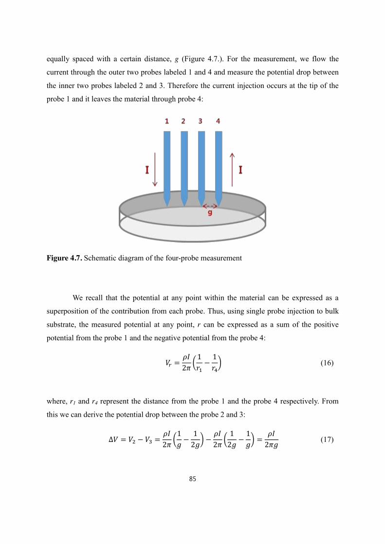
85
equally spaced with a certain distance, g (Figure 4.7.). For the measurement, we flow the
current through the outer two probes labeled 1 and 4 and measure the potential drop between
the inner two probes labeled 2 and 3. Therefore the current injection occurs at the tip of the
probe 1 and it leaves the material through probe 4:
Figure 4.7. Schematic diagram of the four-probe measurement
We recall that the potential at any point within the material can be expressed as a
superposition of the contribution from each probe. Thus, using single probe injection to bulk
substrate, the measured potential at any point, r can be expressed as a sum of the positive
potential from the probe 1 and the negative potential from the probe 4:
( ) (16)
where, r1 and r4 represent the distance from the probe 1 and the probe 4 respectively. From
this we can derive the potential drop between the probe 2 and 3:
( )
( )
(17)
86
In practice, this can be rearranged in terms of resistivity as follows:
( ) (18)
Applying the same calculation steps to the thin film case, the measured potential at any point,
r can be expressed as:
( ) (19)
here, r1 and r4 represent the distance from the probe 1 and the probe 4 respectively and the
potential drop between the probe 2 and 3 is then:
( )
( )
(20)
By rearranging the equation in respect to the sheet resistance Rs, we obtain:
( ) (
) (21)
The result equation is often used as an expression of the sheet resistance for a four-probe
measurement of the thin film semiconductor. Here the spacing between each probe, g is
canceled out through the calculation. Hence, the sheet resistance remains the same
irrespective of the spacing g, as long as the four probes are equally spaced and the spacing, g
is larger enough than the film thickness.
4.2.2 Four-electrode measurement
In our device the electrodes are deposited with a certain configuration. However, the
sheet resistance presented in the previous paragraph is based on the four-probe measurement

87
that does not effectively concern the geometry of the electrodes. For obtaining more accurate
sheet resistance taking account of the geometry of the electrodes, we first simplified the
electrodes to four identical rectangles (Figure 4.8.).
Figure 4.8. Simplified four identical electrodes
The height and the width of the electrodes are α and β respectively and the thickness of the
material is . Then the current density can be expressed as:
( ) (22)
By rearranging Ohm‟s law with this current density, j, we obtain:
( )
(
) (23)
with all the same calculations including the integration and the superposition of the potential
contributions, the result equation is then:
( ) ( ) (24)

88
From this equation we can simply obtain the sheet resistance by putting the slope of
V-I curve recorded from four-probe measurement. For example, the Figure 4.9. shows a V-I
curve for the one of our devices with the Co electrodes deposited by metal evaporation on the
commercial SLG on the silicon wafer. α, β and g are 1,500 μm, 400 μm and 150 μm
respectively while the slope(ΔV/I) is about 78 ohms. Hence the equation eventually gives:
( ) ( ) (25)
Figure 4.9. V-I curve of SLG on Si wafer with Co electrodes evaporated on it
The calculated sheet resistance, 1,354 ohms is within the range of the sheet resistance stated
in the provided specifications (660~1,500 Ω/□) [4].
In most of our experiments, for the devices to be working as a sensor, the device
resistance is monitored as a function of time in order that any external condition changes
could be directly detected and interpreted on the plot. The response of the device is simply
expressed as the changes in device resistance, ΔR/R0.

89
4.3 O2, H2O desorption
The hysteresis electrical behavior of graphene based transistor has been widely
studied by many groups up to now [2,5-7]. Major reason for this is known to be the
adsorption/desorption of water and oxygen molecules [6,8,9]. Most of their experimental
results suggest that the hysteresis is suppressed or vanishes when graphene is placed under
vacuum and pumped-out for extended time but graphene rapidly comes to its initial state
when it is re-exposed to ambient air condition even for relatively short time [6,10]. Similar
result could be observed with our resistive devices. The devices with four identical Cr/Au (10
nm/70 nm) electrodes were used in this measurement. The electrodes were deposited by
shadow-mask thermal evaporation with a 100 μm gap on top of single layer graphene. Figure
4.10. shows the device response and the rate of response variation as a function of time under
vacuum. Here, the response is defined as the ratio of measured resistance, R to the initial
resistance, R0 :
(26)
The rate of response, on the other hand, describes the changes in response per hour:
(27)
Our device was placed in a home-made stainless-steel and high-vacuum (10-6 mbar) capable
chamber, and the measurement was started from the beginning of pumping out the chamber
and lasted for more than 8 hours. The recorded response was almost saturated at 2 % in about
30 minutes at the pressure of 3x10⁻³ mbar with a primary pump. Then it restarts to increase as
we switched from the primary pump to a secondary turbo pump and saturates again at around
6 % after 5 hours at an residual chamber pressure of 1.3x10⁻⁵ mbar. The rate of response
becomes less than 0.5 %/h after 5 hours.

90
Figure 4.10. Time evolution of device resistance changes under vacuum
This change in the device response can be explained if we account for the energy band
diagram of graphene (Figure 4.11.). As stated earlier, graphene on the SiO2 substrate is
commonly behaving as p-doped due to the oxygen and water molecules. Thus the hole
conduction is responsible for the current flowing through graphene layer. The Fermi level is
then below Dirac point where conduction and valence band touches each other. However,
when the device is placed under vacuum for extended time, the oxygen and water molecules
adsorbed on to the graphene surface would be desorbed so that graphene is effectively de-
doped. This de-doping effect translate into the measured increase in device resistance.

91
Figure 4.11 Energy diagram of graphene before and after the desorption of oxygen and water
molecules
4.4 Light exposure response
Desorption of oxygen and water molecules can be further accelerated upon light
exposure above certain wavelength threshold. Figure 4.12 shows how the device response
changes with two different light sources: blue and red diodes with the wavelength of 455 nm
and 633nm respectively. We can distinguish four different stages/scenarios for this
experiment:
(i) First, the device was placed in the chamber and the chamber was being pumped for the
whole measurement. The pressure was lowered to 2x10⁻⁵mbar in first few hours and
stayed the same until the chamber was opened. Here, again, the device response
becomes stable with the rate of response less than 0.5 %/h after about 5 hours as we
expected. For more extended time, the response saturates at around 10 % before we
turn on the light sources.
(ii) Then the light was turned on and the device was exposed to the light with its intensity
of 4 mW/cm2. The intensity was set to be the same for both blue and red light. The
measurement has been carried out at room temperature (20˚C). The results show that
the device response increases with the blue light but not with the red light. The rate of
response shows this result more clearly. When the blue light is on, the rate of response
suddenly increases up to 4.5 %/h and slowly decreases. On the other hand, when the red
light is on, the rate of response stays the same under 0.5 %/h which can be interpreted
as no effective changes in the device response.
(iii) When the light is turned off, the device response didn‟t come down to the values
measured before the light illumination but it rather tends to slightly decrease for the
blue light case, and exhibit no changes for the red light case.
(iv) Finally, the chamber was opened so that the device is exposed to the air. Then the
device response abruptly comes down to the initial value.
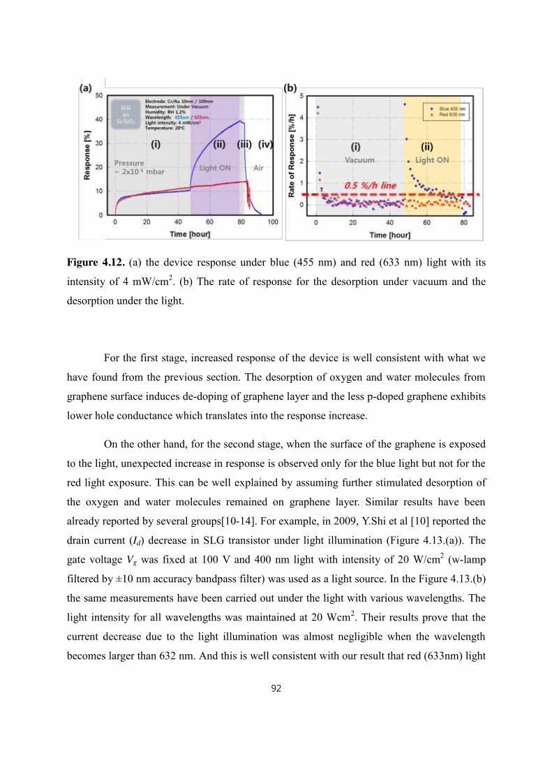
92
Figure 4.12. (a) the device response under blue (455 nm) and red (633 nm) light with its
intensity of 4 mW/cm2. (b) The rate of response for the desorption under vacuum and the
desorption under the light.
For the first stage, increased response of the device is well consistent with what we
have found from the previous section. The desorption of oxygen and water molecules from
graphene surface induces de-doping of graphene layer and the less p-doped graphene exhibits
lower hole conductance which translates into the response increase.
On the other hand, for the second stage, when the surface of the graphene is exposed
to the light, unexpected increase in response is observed only for the blue light but not for the
red light exposure. This can be well explained by assuming further stimulated desorption of
the oxygen and water molecules remained on graphene layer. Similar results have been
already reported by several groups[10-14]. For example, in 2009, Y.Shi et al [10] reported the
drain current (Id) decrease in SLG transistor under light illumination (Figure 4.13.(a)). The
gate voltage Vg was fixed at 100 V and 400 nm light with intensity of 20 W/cm2 (w-lamp
filtered by ±10 nm accuracy bandpass filter) was used as a light source. In the Figure 4.13.(b)
the same measurements have been carried out under the light with various wavelengths. The
light intensity for all wavelengths was maintained at 20 Wcm2. Their results prove that the
current decrease due to the light illumination was almost negligible when the wavelength
becomes larger than 632 nm. And this is well consistent with our result that red (633nm) light

93
couldn‟t effectively change the device resistance.
Figure 4.13. Photoelectrical measurement of the graphene transistor under light illumination:
(a) Drain current change (ΔId) as a function of time for a SLG transistor under an illumination
cycle with 400 nm light (20 W/cm2) at gate voltage Vg = 100 V. (b) Decrease in Id (at Vg =
100 V) for a SLG transistor upon illumination at various wavelengths [10].
Figure 4.14. simply describes the changes in graphene doping by the energy diagram with
Fermi level. Step1 explains the oxygen and water molecules desorption process under
vacuum condition. Graphene as deposited on the SiO2 substrate is p-doped due to the oxygen
and water molecules that can be represented as shifting the Fermi level below Dirac point.
When the device is placed under vacuum for extended time, the oxygen and water molecules
adsorbed on to the graphene surface would be desorbed so that graphene is effectively de-
doped. Resultant de-doped graphene shows increase in device resistance. Step2 is elucidating
further stimulated desorption of the oxygen and water molecules due to the light exposure of
the device. When the surface of the graphene is exposed to the light, further desorption of the
oxygen and water molecules remained on graphene layer will de-dope it. Eventually, less
hole conduction translates into an increase in device resistance.

94
Figure 4.14. Energy diagram of graphene before and after the desorption of oxygen and
water molecules under vacuum and under the light illumination
Furthermore, when the light was tuned off, on the third stage, the device responses
decreased slowly for a few hours in case of the blue light, while it stayed the same level in
case of the red light. Slow decrease in device response is considered to be related to the
possible re-adsorption of desorbed oxygen and water molecules remained in the chamber
even under high-vacuum condition. For the red light, since there was no significative
stimulated desorption, the response stayed the same. Finally, on the last stage, when the
chamber is opened and the device is re-exposed to ambient air condition, the device response
abruptly comes down to the initial value for both blue and red light cases.

95
4.5 Humidity response
4.5.1 Humidity response of the device
Since the device is sensitive to ambient gas molecules such that its response changes
under vacuum or under the light illumination due to desorption of water and oxygen
molecules, it is worth understanding how the device reacts to the relative envrionmental
humidity. The experiments are carried out with an homemade set-up (Figure 4.15.). The
devices were placed on a peltier supported substrate holder in the closed chamber and a
heated bottle of water is installed for supplying water vapor through heated line directly
connected to the chamber. To prevent water vapor from being condensed to water droplets
inside the chamber, the heating temperature of water bottle and the pipe was controlled. The
humidity of the chamber is monitored via a humidity sensor (HC1000-400) while the device
surface temperature was monitored by a the thermocouple. Device response is recorded as a
function of time by four-electrode measurement using Keithley 4200-SCS.
Figure 4.15. Schematic view of the humidity measurement set-up
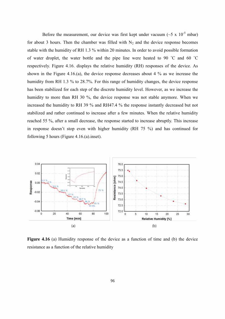
96
Before the measurement, our device was first kept under vacuum (~5 x 10⁻⁵ mbar)
for about 3 hours. Then the chamber was filled with N2 and the device response becomes
stable with the humidity of RH 1.3 % within 20 minutes. In order to avoid possible formation
of water droplet, the water bottle and the pipe line were heated to 90 ˚C and 60 ˚C
respectively. Figure 4.16. displays the relative humidity (RH) responses of the device. As
shown in the Figure 4.16.(a), the device response decreases about 4 % as we increase the
humidity from RH 1.3 % to 28.7%. For this range of humidity changes, the device response
has been stabilized for each step of the discrete humidity level. However, as we increase the
humidity to more than RH 30 %, the device response was not stable anymore. When we
increased the humidity to RH 39 % and RH47.4 % the response instantly decreased but not
stabilized and rather continued to increase after a few minutes. When the relative humidity
reached 55 %, after a small decrease, the response started to increase abruptly. This increase
in response doesn‟t stop even with higher humidity (RH 75 %) and has continued for
following 5 hours (Figure 4.16.(a).inset).
Figure 4.16 (a) Humidity response of the device as a function of time and (b) the device
resistance as a function of the relative humidity

97
The decrease in device response for increase in relative humidity up to around RH
30 % can be interpreted as p-doping caused by adsorption of water molecules on the surface
of graphene [6-10]. However abrupt increase in device response for higher humidity range
cannot be explained by this way.
4.5.2 Vacuum annealing effect
To understand more the results, the device was vacuum annealed at 150 ˚C for 90
minutes and the same experiment has been subsequentely carried out (Figure 4.17.). In this
measurement, however, the device responded totally opposite way to the relative humidity
increase. The response increases about 36% as the humidity increases from RH 1.1 % to RH
54.3 %. After vacuum annealing process, the device response reached about 36 % changes at
RH 54.3 %, while it was only about 4 % at RH 55 % before. The response becomes roughly
about 9 times larger than that from the previous measurement. On the other hand, the device
response saturated at certain humidity level. As shown in the Figure 4.17.(a) the response
saturated and stayed the same as the humidity increased from RH 54.3 % to RH 71 %.
However, it started to decrease again after the saturation level as the humidity increased from
RH 71 % to RH 76.8 %. And this behavior persisted for repeated increase and decrease in
humidity. When we introduced dry N2 into the chamber, the response increased for the first 5
seconds and started to decrease. The first increase is due to the sudden flow of N2 that
temporarily drops the local surface humidity level (Figure 4.17.(d)).

98
Figure 4.17 (a) Humidity response of vacuum annealed device as a function of time and (b)
the device resistance as a function of the relative humidity. (c) Enlarged image for the
humidity response after RH 71% and the N2 flow region. (d) Schematic diagram of the
graphene surface flown by N2.
4.5.3 Surface analysis
To understand what happens under vacuum annealing process, several techniques for
the surface characterization have been applied. Figure 4.18.(a) shows Auger electron
spectroscopy (AES) spectra of our single layer graphene on the glass substrate sample during
vacuum annealing process. RT denotes room temperature while PC and PO indicates the peak
intensity of OKLL and CKLL respectively. The sample was placed in the ultra high vacuum
chamber with the base pressure of about 9 x 10⁻¹⁰ mbar and the substrate temperature was
raised from room temperature to 500 ˚C with 100˚C step increase. AES spectra were recorded

99
for each step and every spectrum clearly shows CKLL and OKLL peak at around 273 eV and
510 eV respectively. The intensity is represented in differentiated form (dN(E)/dE) and
normalized with respect to CKLL peak. The primary electron beam energy used in our
measurement was 2 keV and the over-all set-up energy resolution was 0.3 eV.
Figure 4.18 (a) Differential AES survey spectra evolution of single layer graphene on the
glass substrate during vacuum annealing process from room temperature to 500˚C at the base
pressure of 9 x10⁻¹⁰ mbar. (b) Peak-to-peak intensity ratio between CKLL and OKLL.
Quantitative analysis of AES spectra usually relies on either the peak area of as-
measured curve or the peak-to-peak height of the derivative of the curve. Therefore, the peak
intensity ratio can tell us relative concentrations of the elements on the surface. Figure 4.18.(b)
shows the OKLL to CKLL peak intensity ratio (PO/PC) as a function of the temperature. It
clearly depicts decrease in the oxygen concentrations in graphene layer as we annealed the
sample under vacuum condition. This decrease in oxygen concentration might be due to the
desorption of water molecules and labile oxygen containing functional groups (e.g. epoxide,
carboxylic acid, alcohol, etc.). In addition, since our graphene is synthesized by CVD process
and transferred to the substrate, some chemical contaminations containing oxygen species are
inevitable through the whole synthesis process. Meanwhile, the peak intensity ratio after
annealing (~0.18) is less than half the initial value (~0.38). Based on the fact that our
graphene is not graphene oxide, such a large decrease in oxygen concentration is considered

100
to be more likely related to the desorption of the surface contaminants and adsorbed water
molecules. On the other hand, once the oxygen concentration was decreased at the 100 ˚C
annealing step, it became stable even at higher annealing temperature. Two remarks can be
made on this result. Firstly, the surface contaminations and adsorbed water molecules are not
effectively removed even under UHV condition (~9 x 10⁻¹⁰ mbar). Secondly, even with less
than 100 ˚C annealing, such contaminations and water molecules can be significantely
reduced under vacuum.
Figure 4.19.(a) shows the electron energy loss spectrum (EELS) of our graphene
sample comparing before and after vacuum annealing process. The energy loss peak around 6
eV is known to be attributed to the π-valence band plasmon (π Æ π*) [15]. In 2012, Politano
et al. reported that the water exposed graphene layer shows less pronounced peak at 6 eV than
the pristine graphene (Fig 4.19.(b)) [16]. The presence of C-H and C-OH functional groups
influences the optical absorption of the π plasmon energy range and thereby strongly affect
low-energy plasmon modes [16-18].
8
Figure 4.19. (a) EELS of single layer graphene on the glass substrate before and after
vacuum annealing process from room temperature to 500˚C. (b) EELS for the pristine and
water-exposed single layer graphene/Pt(111) from the literature [16].

101
XPS was also employed for analyzing the effect of vacuum annealing process. Figure
4.20. shows the C1s core-level spectra of the graphene on the glass substrate before (Figure
4.20.(a)) and after vacuum annealing process (Figure 4.20.(b)). A Shirley background
correction was first performed and a Gaussian-Lorentzian peak shape was used for the curve
fitting. The peak corresponding to the sample before vacuum annealing process consists of
two components, one at 284.5 eV binding energy representing the C-C bond of sp2 carbon
[15,19] while the other at 286.6 eV indicating the carbon in C-OH bond [15,19,20]. The
percentage of C-C bond and C-OH bond is 81.5% and 18.5 % respectively. After vacuum
annealing process (Fig 4.20.(b)), the C-OH bonds are removed by the break of labile
functional groups on the graphene surface and the peak fits only with a single C-C bond peak
at 284.5 eV.
Figure 4.20. C1s core-level XPS spectra of single layer graphene on the glass substrate (a)
before and (b) after vacuum annealing process.
4.5.4 Mechanisms of humidity response
Based on the results shown above, we would like to propose a mechanism

102
responsible for the humidity response of our device. Figure 4.21. shows a three-stage
mechanism for the humidity response of the device before vacuum annealing.
First stage describes the initial state of the device before the measurement. The
device was exposed to ambient air conditions for more than 4 weeks before the measurement
and therefore the surface of the graphene is already covered with some water molecules
adsorbed on it. Besides, remaining functional groups through the graphene synthesis and the
device fabrication steps were already forming hydrogen bonds with such water molecules as
well. In 2012, Guo et al. reported the theoretical calculations of the binding energies of water
molecules on graphene materials using a model 32-carbon atom sheet. The calculated binding
energy between pristine graphene and a single water molecule is only about 0.044 eV by
weak Van der Waals, while it is 0.259 eV between hydroxyl groups and a water molecule by
hydrogen bonds [21]. This tells us that the strong hydrogen bonds between water molecules
and the functional groups are relatively stable compared to the weak Van der Waals force for
surface adsorbed water molecules. Therefore, in this state, the humidity response of the
device must be through the surface adsorption rather than hydrogen bonds between functional
groups and the water molecules.
Second stage explains the decrease in device response as the humidity increases.
Functional groups forming hydrogen bonds with water molecules are already almost
saturated and stable compared to the surface adsorption of the water molecules by Van der
Waals interaction. This means that the water molecules prefer to fill uncovered surface of the
device through the surface adsorption. The water molecules adsorbed on the graphene surface
will form a thin water layer with a dipole moment where oxygen atoms pointing toward
graphene induces effective p-doping of the graphene surface [9,22]. Therefore, increased
humidity level from RH 1.3 % to RH 28.7 % results in the decrease in device response.
The last stage is the response inversion where the response increases as the humidity
increases. When the humidity reached RH 28.7 %, the device response tends to not saturate
anymore but to increase. This tendency became stronger as we further increased humidity
level. At this stage, surface adsorption of water molecules is saturated and forms a thin water
layer covering all possible adsorption sites of the graphene surface. Therefore, the effective p-
doping of the graphene surface by a dipole moment saturates as well. The excess of water

103
molecules due to the increased humidity will now form hydrogen bonds with already
adsorbed water molecules covering the surface of the device. These additional hydrogen
bonds are responsible for the observed increase in device response, because it reduces the
effective p-doping of the graphene layer.
Figure 4.21. Schematic diagram of the mechanism for the humidity response of the device
before vacuum annealing.
Figure 4.22. shows another three-stage mechanism for the humidity response of the
device after vacuum annealing. First stage describes again the initial state of the device
before the measurement. The device was annealed at 150 ˚C for 90 minutes under vacuum.
Several groups have already reported that this vacuum annealing process effectively clean the
graphene based device surface [23,24] so that the amount of p-doping is reduced. By such a
process, water molecules adsorbed on the surface of graphene and forming hydrogen bonds

104
with functional groups are effectively removed through the annealing process. In addition,
some labile functional groups are also removed and the surface became cleaner than before.
In the second stage, two different reactions compete each other. First one is the
adsorption of water molecules on the graphene surface which makes graphene be more p-
doped. The other one is the hydrogen bond between water molecules and the functional
groups that reduces the effective p-doping of the graphene layer. Since the latter causes
higher changes in device response, the overall device response increased as we increased the
humidity from RH 1.1 % to RH 54.3 %. After the humidity reached RH 54.3 %, the device
response tends to saturate and not change until we increased it up to RH 71%. This response
saturation can be attributed to the saturated hydrogen bonds between functional groups and
the water molecules.
The last stage is the response inversion. The device is now working like before
vacuum annealing process where the response decreases as the humidity increases. This
inversed response can be attributed to the adsorption of water molecules on the surface of
graphene layer which corresponds to the second stage of the previous results from the device
before vacuum annealing process. Functional groups forming hydrogen bonds with water
molecules are already almost saturated due to the prolonged exposure to humid condition
with continued measurement. Hence the increased relative humidty promotes excessive water
molecules to fill uncovered surface of the device through the surface adsorption thereby
formig a thin water layer that induces effective p-doping of the graphene surface [9,22].

105
Figure 4.22. Schematic diagram of the mechanism for the humidity response of the device
after vacuum annealing.

106
4.6 Conclusions
The test devices were fabricated by simply depositing four identical metal electrodes
on the graphene surface. Three different methods including ink-jet printing, photo-
lithography and shadow-mask evaporation have been studied and the shadow-mask
evaporation was mainly used for the most of our devices because of its simplicity and, most
of all, this method enabled us to avoid possible additional surface contaminations.
On the other hand, the electrical characterization method based on the four-probe
measurement approach has been proposed. Basic four-probe measurement is modified in
order to reflect our electrode configurations in the sheet resistance calculation.
Desorption of the oxygen and water molecules has been investigated to understand
the intrinsic device response. The device response changes under vacuum because of the
desorption of ambient water and oxygen molecules already adsorbed on to the graphene
surface. This behavior could be further increased as we shine the device with the blue light
(455 nm). The humidity response of the device has been also studied with the effect of
vacuum annealing process. Electron spectroscopy such as XPS, AES and EELS have been
employed to understand the mechanism of the vacuum annealing process. We proposed three-
stage mechanism that is responsible for the humidity response of the device before and after
the vacuum annealing process.
The presented studies on the desorption of water and oxygen molecules provide a
preliminary understanding of the intrinsic response of the graphene based gas sensing device.
When the graphene is directly exposed to the ambient air, the effects from the adsorption of
such molecules are appreciable such that the device response is inversed in our case.
Therefore, it is worth noting that the effects of ambient air needs to be taken into account
before characterizing the gas sensing behavior of the device. Alternatively, one can develop
the passivation methods to prevent graphene from ambient air. But this might be very tricky
because the active area should still be exposed to the target gas molecules while the rest is
passivated.

107
Reference
[1] Madhav Gautam, Ahalapitiya H. Jayatissa, Gas sensing properties of graphene
synthesized by chemical vapor deposition, Materials Science and Engineering C 31 (2011)
1405-1411.
[2] Hua Xu, Yabin Chen, Jin Zhang, and Haoli Zhang, Investigating the Mechanism of
Hysterisis Effect in Graphene Electrical Field Device Fabricated on SiO2 Substrates using
Raman Spectroscopy, small 2012, 8, No.18, 2833-2840
[3] A.Verdaguer, C.Weis, G.Oncins, G.Ketteler, H.Bluhm, M.Salmeron, Growth and Structure
of Water on SiO2 Films on Si Investigated by Kelvin Probe Microscopy and in Situ※ray
Spectroscopies, Langmuir 2007, 23, 9699.
[4] https://graphene-supermarket.com/Monolayer-Graphene-on-a--285-nm-Silicon-Dioxide-
Wafer-5-pack.html
[5] Haomin Wang, Yihong Wu, Chunxiao Cong, Jingzhi Shang, and Ting Yu, Hysteresis of
Electronic Transport in Graphene Transistors, Vol. 4, No.12, 7221-7228, 2010, ACS NANO.
[6] Myrsini Lafkioti, Benjamin Krauss, Timm Lohmann, Ute Zschieschang, Hagen Klauk,
Klaus v. Klitzing, and Jurgen H. Smet, Graphene on a Hydrophobic Substrate: Doping
Reduction and Hysteresis Suppression under Ambient Conditions, Nano Lett. 2010, 10, 1149-
1153
[7] Timm Lohmann, Klaus von Klitzing and Jurgen H.Smet, Four-Terminal Magneto-
Transport in Graphene p-n Junction Created by Spatially Selective Doping, Nano Lett. 2009,
9, 1973
[8] J.Moser, A.Barreiro and A.Bachtold, Current-induced cleaning of graphene, Appl. Phys.
Lett. 2007, 91, 163513.
[9] J.Moser, A.Verdaguer, D.Jimenez, A.Barreiro, and A.Bachtold, The environment of
graphene probed by electrostatic force microscopy, Applied Physics Letters 92, 123507 (2008)
[10] Yumeng Shi, Wenjing Fang, Keke Zhang, Wenjing Zhang, and Lain-Joing Li,

108
Photoelectrical Response in Single-Layer Graphene Tansistors, small 2009, 5, No. 17, 2005-
2011
[11] Artjom Berholts, Tauno Kahro, Aare Floren, Harry Alles, and Raivo Jaaniso, Photo-
activated oxygen sensitivity of graphene at room temperature, APPLIED PHYSICS
LETTERS 105, 163111 (2014)
[12] Jian Lin, Jiebin Zhong, Jennifer Reiber Kyle, Miroslav Penchev, Mihri Ozkan and
Cengiz S Ozkan, Molecular absorption and photodesorption in pristine and functionalized
large-area graphene layers, Nanotechnology 22 (2011) 355701
[13] Gugang Chen, Tereza M. Paronyan, and Avetik R. Harutyunyan, Sub-ppt gas detection
with pristine graphene, APPLIED PHYSICS LETTERS 101, 053119 (2012)
[14] Chandan Biswas, Fethullah Günes, Duong Dinh Loc , Seong Chu Lim, Mun Seok Jeong,
Didier Pribat, and Young Hee Lee, Negative and Positive Persistent Photoconductance in
Graphene, Nano Lett. 2011, 11, 4682–4687
[15] A.Siokou, F.Ravani, S.Karakalos, O.Frank, M.Kalbac, C.Galiotis, Surface refinement
and electronic properties of graphene layers grown on copper substrate: An XPS, UPS and
EELS study, Applied Surface Science 257 (2011) 9785-9790.
[16] A.Politano, A.R.Marino, and G.Chiarello, Effects of a humid environment on the sheet
plasmon resonance in epitaxial graphene, Physical Review B 86, 085420 (2012)
[17] U.Bangert, C.T.Pan, R.R.Nair, and M.H.Gass, Structure of hydrogen-dosed graphene
deduced from low electron energy loss characteristics and density functional calculations,
Appl.Phys. Lett. 97, 253118 (2010)
[18] Zhiqiang Luo, Jingzhi Shang, Sanhua Lim, Dehui Li, Qihua Xiong, Zexiang Shen, Jianyl
Lin and Ting Yu, Modulating the electronic structures of graphene by controllable
hydrogenation, Appl. Phys. Lett. 97, 233111 (2010).
[19] Nam Han, Tran Viet Cuong, Min Han, Beo Deul Ryu, S.Chandramohan, Jong Bae Park,
Ji Hye Kang, Young-Jae Park, Kang Bok Ko, Hee Yun Kim, Hyun Kyu Kim, Jae Hyoung
Ryu, Y.S.Katharria, Chel-Jong Choi and Chang-Hee Hong, Improved heat dissipation in

109
gallium nitride light-emitting diodes with embedded graphene oxide pattern, Nature
communications 4:41452 DOI: 10.1038/ncomms2448
[20] V.Datsyk, M.Kalyva, K.Papagelis, J.Parthenios, D.Tasis, A.Siokou, I.Kallitsis, C.Galiotis,
Chemical oxidation of multiwalled carbon nanotubes, Carbon 46 (2008) 833.
[21] L.Guo, H.-B. Jiang, RQ Shao, Y.-L. Zhang, S.-Y.Xie, J.-N.Wang, X.-B.Li, F.Jiang, Q.-
D.Chen, T.Zhang, H.-B. Sun, Two-beam-laser interference mediated reduction, pattering and
nanostructureing of graphene oxide for the production of a flexible humidity sensing device,
Carbon 50 (2012) 1667-1673.
[22] O.Leenaerts, B.Partoens, and F.M.Peeters, Water on graphene: Hydrophobicity and
dipole moment using density functional theory, Physcal Review B 79, 235440, 2009
[23] Konstantions Alexandrou, Filippos Farmakis, Alexandros Arapis, and Nikolaos
Georgoulas, Yufeng Hao and James Hone, Ioannis Kymissis, Effect of vacuum thermal
annealing to encapsulated graphene field effect transistors, J.Vac.Sci,Technol.B 34(4),
Jul/Aug 2016
[24] Pierre L. Levesque, Shadi S.Sabri, Carla M.Aguirre, Jonathan Guillemette, Mohamed
Siaj, Patrick Desjardins, Thomas Szkopek, and Richard Martel, Probing charge transfer at
surfaces using graphene transistors, Nano Lett. 2011, 11. 132-137
\

110
Chapter V
Functionalization
Chapter V. Functionalization ............................................................................................................... 111
5.1 Generalities ................................................................................................................................... 111
5.2 Ruthenium Complex(Blue) ........................................................................................................... 111
5.3 Functionalization of the device ..................................................................................................... 114
5.3.1 Functionalization of the device ............................................................................................. 114
5.3.2 Photoresponse of the functionalized device .......................................................................... 114
5.4 Double interfaces responses .......................................................................................................... 121
5.4.1 Inversed response. ................................................................................................................. 126
5.4.1.1 Intensity dependency of the inversed response under vacuum ..................................... 126
5.4.1.2 Duty cycle dependency of the inversed response under vacuum.................................. 128
5.4.2 Charge transfer ...................................................................................................................... 130
5.5 Conclusions ................................................................................................................................... 135
Reference ............................................................................................................................................ 136

111
Chapter V. Functionalization
5.1 Generalities
Graphene is often functionalized with various elements for many purposes such as
improvement of sensitivity, specificity, solubility, loading capacity, etc [1-8]. For our device,
especially for sensing applications, improved sensitivity and specificity is the main purpose
of the functionalization. We functionalized graphene surface by non-covalent way in order to
avoid altering the native electronic structures and to preserve the intrinsic properties of the
graphene. Pyrene moiety has been employed as a linker between the functional molecules and
the graphene surface. It has been reported to have a strong affinity toward graphene surface
via strong π-π interaction [9,10].
5.2 Ruthenium Complex(Blue)
Recently, the Ru(II) complexes have received a wide attention due to their excellent
properties such as good electrochemical stability, high sensitivity, and high electrogenerated
chemiluminescence (ECL) efficiency under moderate conditions [11,12]. It is also employed
in donor-acceptor assemblies thanks to its photostability and high metal ligand conductor
transfer (MLCT) excited-state energy [13,14]. Benefiting from all these exceptional
properties, some studies on the functionalization of graphene materials with the Ru(II)
complexes have been reported. Li et al. have reported the studies on the immobilization of
[Ru(bpy)3]2+ and the [Ru(bpy)3]2+-graphene-Nafion modified electrode which result in good
sensitivity and stability for the ECL applications [15]. Zhang et al. have also reported that the
Ru(II) complexes were well assembled onto the graphene oxide (GO) surface by forming
amide bond. The charge transfer from the excited ruthenium to GO was explained by
fluorescence spectra and photocurrent response measurements [16]. While these works were
mainly based on the covalent bond functionalization method, an investigation of graphene
non-covalently functionalized with Ru(II) complexes has been also reported by Li et al [17].
In their work, the Ru(II) complexes have been successfully anchored on graphene sheets
utilizing a simple π-π stacking self-assembly noncovalent strategy for the use of ECL
materials and photosensors.

112
In this thesis, we report the non-covalent assembly of the Ru(II) complexes
([Ru(bpy)3]2+) functionalized with a pyrene unit as anchoring module (Figure 5.1.). Thanks to
the anchoring module, [Ru(bpy)3]2+ could be spatially separated from the graphene surface.
This spatial separation prevents the direct charge recombination pathways between the
complexes and the graphene layer, and thereby increases the lifetime of the light induced
state of the complexes [18].
Figure 5.1. Schematic view of Ru(II) tris bipyridine complex. [RuII-Pyr]2+
The synthesis of the complex has been carried out at Institut de Chimie Moléculaire
et des Matériaux d‟Orsay (ICMMO). The complexes are characterized and the UV-visible
spectrum of the complex has shown an absorption maximum at 455nm, corresponding to the
Metal to Ligand Charge Transfer (MLCT) of the [Ru(bpy)3]2+ chromophore [18]. Excitation
of this complex in acetonitrile at 455 nm with a nanosecond laser flash leads to formation of
an exicted state, which is detected by emission spectra with a maximum at 618 nm, typical
for Ru(II)-polypyridine complexes. However, the emission lifetime is significantly longer
(1.0 μs/20% and 4.7 μs/80%) than observed in [Ru(bpy)3]2+ (0.8 μs). This is attributed to the
fast establishment of an equilibrium between [Ru(bpy)3]2+* and pyrene* triplet excited states
[19]. The lifetime of the emission is independent of the detection wavelength. The excited

113
state-ground state absorption difference spectrum shows bleaching at 350 nm and a maximum
at about 417 nm attributed to the formation of the excited state of the pyrene. While the
decrease in the absorption at about 455 nm is expected due to the bleaching of the Ru(II) to
bipyridine MLCT state due to the formation of some Ru(II) in the triplet excited state.
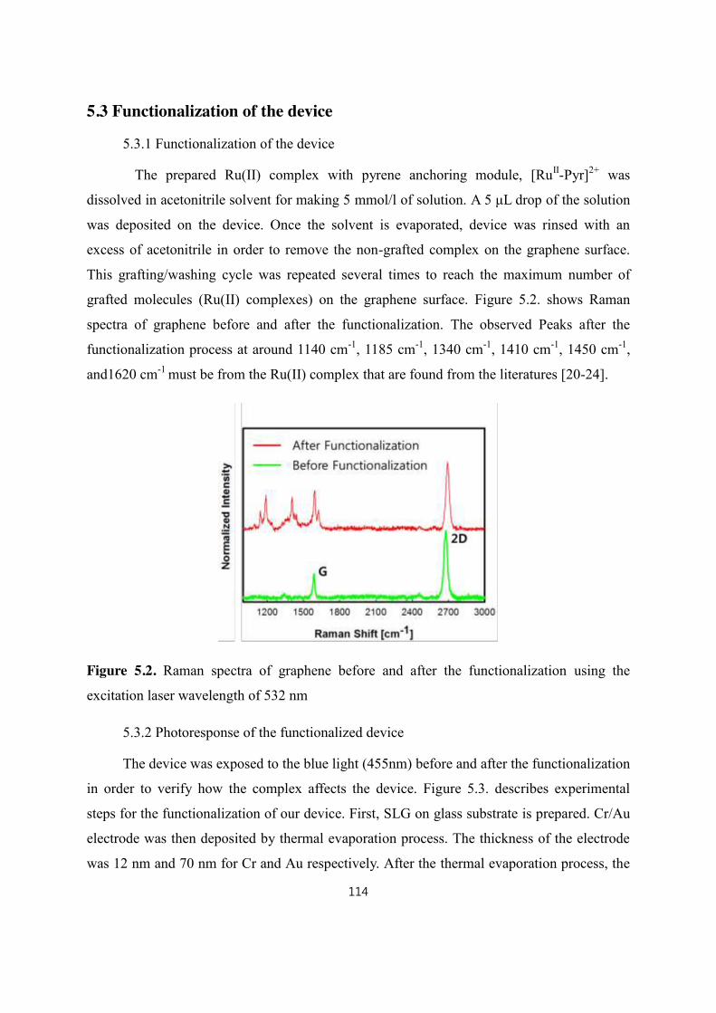
114
5.3 Functionalization of the device
5.3.1 Functionalization of the device
The prepared Ru(II) complex with pyrene anchoring module, [RuII-Pyr]2+ was
dissolved in acetonitrile solvent for making 5 mmol/l of solution. A 5 μL drop of the solution
was deposited on the device. Once the solvent is evaporated, device was rinsed with an
excess of acetonitrile in order to remove the non-grafted complex on the graphene surface.
This grafting/washing cycle was repeated several times to reach the maximum number of
grafted molecules (Ru(II) complexes) on the graphene surface. Figure 5.2. shows Raman
spectra of graphene before and after the functionalization. The observed Peaks after the
functionalization process at around 1140 cm-1, 1185 cm-1, 1340 cm-1, 1410 cm-1, 1450 cm-1,
and1620 cm-1 must be from the Ru(II) complex that are found from the literatures [20-24].
Figure 5.2. Raman spectra of graphene before and after the functionalization using the
excitation laser wavelength of 532 nm
5.3.2 Photoresponse of the functionalized device
The device was exposed to the blue light (455nm) before and after the functionalization
in order to verify how the complex affects the device. Figure 5.3. describes experimental
steps for the functionalization of our device. First, SLG on glass substrate is prepared. Cr/Au
electrode was then deposited by thermal evaporation process. The thickness of the electrode
was 12 nm and 70 nm for Cr and Au respectively. After the thermal evaporation process, the

115
device was annealed at 150 ˚C for 90 minutes under vacuum conditions to improve electrode
contact and to remove residual contaminations on the graphene surface. Then this device is
exposed to the blue light (455nm) to see its intrinsic photoresponse. The device is then
functionalized with ruthenium complex as stated above. The functionalized device is exposed
again to the blue light to see the effect of the functionalization with the Ru(II) complexes.
Figure 5.3. Experimental steps for the functionalization of the graphene based resistive
sensor and its light response
The device was functionalized 6 times in this way and the Figure 5.4.(a) presents the
blue light response of the device measured right after each functionalization process. First,
the light was turned on after 500 sec and it was repeatedly turned on and off for each 5
minute. Up to 3 times of repeated functionalization process, the device response generally
increased up to 160 %. However, additional steps of functionalization process made device
response to decrease again. After the fifth functionalization, the response becomes
comparable to that of after the first functionalization step.
Figure 5.4.(d) shows the changes in initial device resistances after each
functionalization process. The initial device resistance was about 15 ohms before the

116
functionalization, but it increased to about 45 ohms after the first functionalization process.
This increased resistance stayed in the similar values range (43~51 ohms) after following
additional functionalization processes. The increase in the device resistance implies that the
complexes are interacting with the current flow by acting as scattering centers [25]. However,
the fact that there was no appreciable increase for the successive measurements after the first
functionalization step implies that the graphene surface is effectively functionalized with the
complexes starting from the first functionalization process.
On the other hand, after graphene is well functionalized with the complexes, the
device started to show different behaviors under the light illumination. Figure 5.4.(b) shows
detailed device response after 3 times of functionalization in the Figure 5.4.(a). The signal
shape exhibit a first abrupt increase in the device response followed by the slower increase in
device response due to the photo induced desorption of water and oxygen molecules [26-30].

117
Figure 5.4. (a) Light response of the graphene resistive sensor functionalized with the
ruthenium complex. (b) Two different mechanism responsible for the light response of the
device. (c) Rate of response. (d) Initial device resistances after each functionalization process.
The light source with the wavelength of 455nm and the intensity of 1.1mw/cm2 is used.
To further understand the photo-response and photo-desorption effects separately we
performed two different measurements by varying the intensity and the frequency of the
incident light source. Figure 5.5. shows the device response with varying the intensity of the
light source. The blue light (455 nm) source was controlled with a function generator HM
8130. The light pulse with the frequency of 0.05 Hz and the 50 % of duty cycle was applied
while the electrical measurement speed was about 1 measuring point every 85 ms. Three
different light intensities were tested: 0.57 mW/cm2, 1.1 mW/cm2, and 12.3 mW/cm2. It is
clearly shown that the global device response increases as we increase the light intensity.

118
Figure 5.5. Light response of the device with different light intensities: (a) 0.57 mW/cm2, (b)
1.1 mW/cm2, (c) 12.3 mW/cm2. (d) The global increase in response and the variation with
different light intensities. The wavelength of the light source was 455nm.
For the light intensity of 0.57 mW/cm2, the device response increased about up to
4.3 % and showed about 2.2 % variation upon the repeated light exposures (Figure 5.5.(a)).
For the light intensity of 1.1 mW/cm2, the response increased to 4.3 % for the first light pulse,
and then continuous and slight increase in response up to about 5.4 % upon 12 times of
repeated exposures was observable (Fig 5.5.(b)). The variations in the response for one pulse
was about 2.3 % which is the same as that for the intensity of 0.57 mW/cm2. However, for the
higher light intensity of 12.3 mW/cm2, the device showed much stronger increase in response
up to about 18.7 % upon 12 times of repeated exposures (Figure 5.5.(c)). For the first light
pulse, the response increased about 7 % and the variations for each light pulse was about
3.7 %. Figure 5.5.(d) compares the global response increases and the variations of the device
upon 12 times of repeated exposures to the light with three different intensities. They are all
affected by the increased light intensity. However, it is clear that the global increase in the
device response is much more dependent on the light intensity than the variation which is
considered to be attributed to the photo-desorption of the water and oxygen molecules
adsorbed on the graphene surface [26-30].
Figure 5.6. shows the light response of the device with different pulse frequencies.
The light intensity and the duty cycle of the pulse were fixed at 1.1 mW/cm2 and 50 %
respectively. The measurement speed was about 1 point per 85 ms which is the fastest limit of
the set-up.

119
Figure 5.6. Light response of the device with different light pulse frequencies: (a) 1 Hz with
inset showing zoomed region, (b) 0.1 Hz, (c) 0.05 Hz. (d) The global increase in response and
the variation with different pulse frequencies. The wavelength of the light source was 455nm.
Figure 5.6.(a) shows that the response is fast enough to follow the 1 Hz pulse of light
which cannot be explained by the photo-desorption response of the intrinsic graphene
because of its low adsorption/desorption rate. However, the response for each light pulse does
not saturate with this fast measurement while it saturates with 0.1 Hz pulse of the light
(Figure 5.6.(b)). This means that it requires at least 5 sec to have saturated response for a
pulse of the light. Meanwhile, the global response increase and the variation of the response
also changes as the pulse frequency changes. Unlike intensity dependency result, the
variation of the response was affected stronger than the global increase in the response by the
frequency changes (Figure 5.6.(d)).

120
As the device response upon the light exposure clearly shows difference in the rate of
response, there must be, at least, two different mechanisms responsible for the device
response. One can be related to the desorption of water and oxygen molecules that happens
both for intrinsic and functionalized device. The device shows persistent response increase
with relatively low rate of response after the first few seconds as the light was illuminated on
the surface of the graphene. This is attributed to the global increase in device response.
Higher intensity of the light promotes more desorption of the water and oxygen molecules so
that the appreciable global increase in device response appears.
Another mechanism which can be responsible for the abrupt increase in device
response for the first few seconds of light illumination might be explained by the charge
transfer from the complexes to the graphene [16,17,31]. The Figure 5.7. shows the schematic
view of this charge transfer. Under the light illumination, the [Ru(bpy)3]2+ triplet excited
states are formed. Charges from this excited states travel to the pyrene anchoring groups and
trigger the excited state of the pyrene units. The secondary charge transfer from the excited
pyrene units to the graphene follows. As mentioned earlier, graphene on the SiO2 is p-type
material where the hole conduction is responsible for the current flow in the device [32-34].
The photo-excited electrons flow coming from the anchored complexes recombine with holes
in graphene and thereby induce de-doping of the material. This reaction happens much faster
than the desorption process and therefore the device response increases abruptly in the first
few seconds as the light is turned on.
Figure 5.7. Schematic view of the mechanism of electron transfer from the excited
complexes to the graphene via pyrene units.

121
5.4 Double interfaces responses
In the previous paragraphs, we showed that graphene can be well functionalized with
Ru(II) complexes and the charge transfer from the complex to the graphene under
illumination has been studied. In this paragraph, another device has been fabricated utilizing
the functionalized graphene. The Figure 5.8. shows the fabrication of a double-interface
device based on the functionalized graphene and its light response experiment. First, SLG on
glass substrate is prepared. It is annealed at 150 ˚C for 90 minutes under vacuum. Then the
device is functionalized with ruthenium complexes following the same method used before.
Cr/Au electrodes are subsequentely deposited by shadow-mask thermal evaporation process.
The thickness of the electrode was 10 nm and 70 nm for Cr and Au respectively. After the
thermal evaporation process, the device was annealed again at 150 ˚C for 90 minutes under
vacuum conditions to improve electrode contact and to remove residual contaminations on
the graphene surface. The device now has two different interfaces: graphene-to-pyrene, Ru(II)
complex-to-metal. We named it double-interface device. Then this device is exposed to the
blue light (455nm) to see the effect of the interactions at two different interfaces.
Figure 5.8. Experimental steps for fabrication of the double-interface device based on the
functionalized graphene and its light response

122
Figure 5.9. shows the schematic view of the double-interface device. The first
interface is between chromium and the Ru(II) complex while the second interface is between
the Ru(II) complex and the graphene layer. Since the Ru(II) complexes are spatially separated
from the graphene surface due to the pyrene units, what is actually touching the graphene for
the second interface is the pyrene units via non-covalent π-π stacking.
Figure 5.9. Schematic view of the double-interface device
Figure 5.10. shows the double-interface device response at varying intensity of the
light source. The blue light (455 nm) source was controlled by the function generator HM
8130. The light pulse with the frequency of 0.1 Hz and the 50 % of duty cycle was applied
while the measurement speed was about 1 measuring point per 85 ms. The measurements
were carried out at room temperature under N2 condition. Four different light intensities were
tested: 0.05 mW/cm2, 0.57 mW/cm2, 1.1 mW/cm2, and 5 mW/cm2. Starting with the light
intensity of 0.05 mW/cm2 Figure 5.10.(a), device shows similar behavior to that of single
interface device as we increased the light intensity to 0.57 mW/cm2 (Figure 5.10.(b)). Both

123
the global device response and the fast variation increase was observed. However, as we
further increase the light intensity to 1.1 mW/cm2 (Figure 5.10.(c)), the tendency of this
increase started to saturate. When the higher light intensity of 5 mW/cm2 was used, during
one measurement, the device response inversed (Figure 5.10.(d)).
Figure 5.10. Light response of the double-interface device with different light intensities: (a)
0.05 mW/cm2, (b) 0.57 mW/cm2, (c) 1.1 mW/cm2, (d) 5 mW/cm2. The wavelength of the
light source was 455 nm.
Figure 5.11. shows the enlarged view of the Figure 5.10.(d) to show the transition of
the device response. For the beginning of the measurement, the device shows normal
response. The device response increases as the light is turned on. However, the fast variation
tends to decrease and the global device response also tends to saturate (Fig 5.11.(b)). After a
while the device enters in a transition region. In this region, the global device response only

124
decreases upon the light illumination and almost no fast variation is observed (Figure 5.11.
(c)). As the measurement continues, the fast response started to be inversed and showed
exactly the opposite behavior compared with beginning. The device fast response decreases
as the light is turned on. Also the fast variation tends to increase while the global device
response continues to decrease (Figure 5.11.(d)). However, as soon as the device is exposed
to ambient air condition, the responses come back to normal response. This is remarkable as
the device response inversed within 5 minutes of measurement without any experimental
condition changes.
Figure 5.11. (a) Response of the double-interface device illuminated with the 455 nm and
5mW/cm2 light. (b) Normal response region. (c) Transition region. (d) Inversed response
region.
The device response inversion was reproducible. Repeated measurement under N2
(Figure 5.12.(a)) shows the same result. The same measurement has been also carried out

125
under vacuum condition (Figure 5.12.(b)). The device was placed in the chamber filled with
N2 and the chamber was pumped out until the pressure reached to 3.7 x 10⁻⁵ mbar. At this
pressure, the device response inversed again.
To facilitate the response inversion, the light with higher intensity (12.3 mW/cm2)
and longer period (0.01 Hz, 50 % duty cycle) was illuminated on the device (Figure 5.12.(c))
under N2 condition. In this case, the device response inversed with only three pulses of the
light. The same measurement has been carried out under ambient air condition Figure
5.12.(d). But in this case, the response did not inverse but showed step increase followed by
the global device response decrease under the light illumination.
Figure 5.12. Response inversion test (a) under N2 and (b) under vacuum (3.7 x 10⁻⁵ mbar)
condition with 0.1 Hz pulse of the 455 nm and 5 mW/cm2 light. Response inversion test (c)
under N2 and (d) under ambient air condition with 0.01 Hz of the 455 nm and 12.3 mW/cm2
light.

126
The results from this series of measurements are suggesting us two important issues
on the device response inversion:
9 Response inversion occurs when the water and oxygen molecules are desorbed
9 Electron transfer from Ru(II) complexes to the metal electrode
First, the fact that the response inversion occurs only under N2 and vacuum condition but
not under ambient air condition suggest that the water and oxygen molecules have to be
desorbed before the response inversion. In addition, the response inversion happens only
when the global response increase reches saturated regime and started decreasing which must
be because of the effective desorption of water and oxygen molecules.
Second, the device response decreases under the light illumination after it reaches
inversion. This indicates that the graphene is more p-doped. For this to happen, electrons
from the excited state of the Ru(II) complexes have to transfer to the metal electrode that is
the opposite charge flows compared to that of the one interface device. This suggests that the
electronic states of the first interface between Ru(II) complexes and adhesion layer might
have been positively charged during the measurement, so that the excited electrons are
attracted more to the the first interface. One hypothesis can be set up based on the possible
oxidation of the adhesion layer. It is well-known that Cr is relatively easily oxidized at room
temperature [35-38]. If the Cr layer is oxidized to form positive chromium oxide layer,
electrons will travel to this layer than to the graphene film, resulting in more p-doping of the
graphene film. Detailed investigation on this hypothesis is discussed in 5.4.2 Chrage transfer.
5.4.1 Inversed response.
5.4.1.1 Intensity dependency of the inversed response under vacuum
Once the device response is inversed, before the device is exposed to ambient air
condition, this inversed response was persistent. Figure 5.13. shows the light intensity
dependency of the inversed response of the device. Like the previous experiments, the 455
nm light source was controlled by the function generator HM 8130 and the light pulse with

127
the frequency of 0.1 Hz and the 50 % of duty cycle was applied. The measurement speed was
about 1 point per 85 ms. Six different light intensities were tested: 0.05 mW/cm2, 0.57
mW/cm2, 1.1 mW/cm2, 5 mW/cm2 11 mW/cm2, and 12.3 mW/cm2.
Figure 5.13 Intensity dependency of the inversed response under vacuum (3 x 10⁻⁵ mbar).
Light intensities vary: (a) 12.3 mW/cm2, (b) 11 mW/cm2, 5 mW/cm2, 1.1 mW/cm2, 0.57
mW/cm2, 0.05 mW/cm2 with 0.1 Hz pulse of the 455 nm.

128
For the higher light intensities, it is clearly shown that the global device response
decrease tends to increase from 0.8 % to 3.2 % as we increase the light intensity from 5
mW/cm2 to 12.3 mW/cm2 while it doesn‟t change for the lower light intensities under 1.1
mW/cm2 (Figure 5.14.). However, the variation of the response shows exactly the opposite
behavior. It saturates at 0.6 % higher light intensities, and decreases for lower light intensities
to 0.1 % with 0.05 mW/cm2 (Figure 5.14.).
Figure 5.14. Intensity dependency of the double-interface device
5.4.1.2 Duty cycle dependency of the inversed response under vacuum
Figure 5.15. shows the duty cycle dependency of the inversed response of the device.
The 455 nm light source with the intensity of 12.3 mW/cm2 was controlled by the function
generator HM 8130. The light pulse frequency was 0.1 Hz. The duty cycle of the pulse was
changed from 2 % to 50 % and the measurement speed was about 1 point per 85 ms.
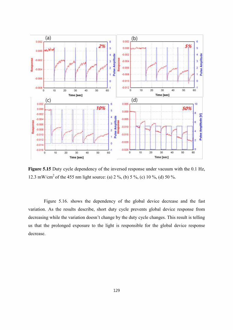
129
Figure 5.15 Duty cycle dependency of the inversed response under vacuum with the 0.1 Hz,
12.3 mW/cm2 of the 455 nm light source: (a) 2 %, (b) 5 %, (c) 10 %, (d) 50 %.
Figure 5.16. shows the dependency of the global device decrease and the fast
variation. As the results describe, short duty cycle prevents global device response from
decreasing while the variation doesn‟t change by the duty cycle changes. This result is telling
us that the prolonged exposure to the light is responsible for the global device response
decrease.

130
Figure 5.16 Duty cycle dependency of the inversed response under vacuum with the 0.1 Hz,
12.3 mW/cm2 of the 455 nm light source.
5.4.2 Charge transfer
To understand the mechanism behind the inversed response of the double-interface
device, we tried two more different interfaces by changing the Cr adhesion layer used : Ni
and Ti. 10 nm of Ni and Ti layers are deposited onto the functionalized graphene by e-beam
evaporation followed by 70 nm of Au metal electrode deposition. After the electrode
deposition, the devices were annealed at 150 ˚C for 90 minutes under vacuum.
Figure 5.17.(a) shows the as-fabricated device response with Ni as an adhesion layer
under N2 condition. The 455 nm light source with the intensity of 12.3 mW/cm2 was
controlled by the function generator HM 8130. The frequency of 0.1 Hz with the duty cycle
of 50 % was applied. The measurement speed was about 1 measuring point per 85 ms. The
device response shows both the global device response increase and the step increase as the
light is illuminated. The light illumination continued for several hours but no inversion has
been observed. The device was exposed to ambient air condition for 3 days and measured
again (Figure 5.17.(b)). In the beginning of the measurement, the global device response
increases as the light is illuminated and the response stayed the same when the light was
turned off (Figure 5.17.(c)). However, no step increase was observed which resembles to the

131
result observed for the photo-desorption of the water and oxygen molecules. After a while
device started to show step decrease upon the light illumination while the global device
response increase continues (Figure 5.17.(d)). This result indicates that the adsorbed water
and oxygen molecules are playing important role for the device response inversion.
The Figure 5.17.(e,f) shows the response of the device with Ti layer measured under N2
as-fabricated and 3 days later respectively. The global device response increases for both as-
fabricated and 3 days later measurements and the step increase of the response upon the light
illumination is also observed. However, even with prolonged measurement, the device with
Ti layer didn‟t show response inversion.

132
Figure 5.17. Response of the double-interface device with Ni as an adhesion layer for (a) as-
fabricated and (b) after 3 days of exposure to an ambient air condition. Zoomed region of (b)
for (c) the normal response in the beginning and (d) the inversed response. Response of the
double-interface device with Ti as an adhesion layer for (e) as-fabricated and (f) after 3 days.
Measurements are carried out under N2 condition with 0.1 Hz pulse of the 455 nm and 12.3
mW/cm2 light.

133
Based on the results shown above, we propose two mechanisms responsible for the
response of the double-interface device. One is for explaining the “normal” response and the
other is related to the inversed response. Figure 5.18. shows a schematic diagram explaining
the normal response of the device under the light before the response inversion regime. For
the normal response, the response increases because of two reasons:
(i) Desorption of water and oxygen molecules
(ii) Charge transfer from the excited Ru(II) complexes to the graphene
Since the graphene on the SiO2 substrate is p-doped in ambient conditions, the hole
conduction is responsible for the current flowing through the layer. As the water and oxygen
molecules desorbe from the graphene surface, graphene becomes less p-doped and this
translates into the device response increase. This desorption is mainly responsible for the
global device response increase which saturates before the response inversion occurs. The
second reason relates to the charge transfer from the excited Ru(II) complexes to the
graphene. As the electrons traveled to the graphene layer and recombine with the holes, the
conductance of the device decreases which in turn increases the device response.
Figure 5.18. Schematic diagram for the normal response of the double-interface device

134
The schematic diagram for the second mechanism explaining the inversed response
of the device is represented in the Figure 5.19.. In this case, the charge transfer is the main
reason for the decrease in device response. However, the flow of excited electrons from the
Ru(II) complexes travel to the metal electrode rather than to the graphene layer. For this to be
happened the adhesion layer must be oxidized. Chromium and Nickel are relatively easy to
be oxidized at room temperature in ambient air condition than Titanium [35-38]. Therefore,
the response inversion was observable only for the device with Cr and Ni as an adhesion
layer but not with Ti. Furthermore, the fact that the response inversion didn‟t happen for
pristine as-fabricated device explains that the adsorbed water and oxygen molecules are
necessary for the oxidation of the adhesion layer.
Figure 5.19. Schematic diagram for the normal response of the double-interface device

135
5.5 Conclusions
In this study, graphene was functionalized with [RuII-Pyr]2+ complex by non-covalent
way in order to avoid altering the native electronic structures and preserve the intrinsic
properties of graphene. Pyrene moiety has been employed as a linker between the functional
molecules and the graphene surface.
Functionalized graphene based resistive sensor was fabricated by functionalizing the
device with pre-deposited contact electrodes. The light response of the device has been
investigated with the 455 nm blue light. The light response of the functionalized device
shows instant increase under the light illumination due to the charge transfer between the
complexes and the graphene film that is not observable with non-functionalized device.
Electrons transferred from the excited Ru(II) complexes to the graphene film under the light
illumination enhanced the response of the device. A slow and global increase in the device
response under the light illumination is attributed to the photo-desorption of water and
oxygen molecules adsorbed onto the surface.
Double-interface device was fabricated by depositing four identical electrodes on the
pre-functionalized graphene surface. The first interface is between the adhesion layer of the
metal electrode and the Ru(II) complex while the second interface is between the Ru(II)
complex and the graphene layer. The response of the device under the 455 nm blue light
illumination is inversed due to the changes in charge transfer flow orientation. In the
beginning, the electrons transferred from the excited Ru(II) complexes to the graphene film
under the light illumination enhanced the response of the device. However, as the
measurement continues, the adhesion layer of the metal electrode is oxidized under the light
illumination, and act as an electron acceptor thus the electrons from the excited Ru(II)
complexes travel to the oxidized adhesion layer resulting in the inversed response of the
device.

136
Reference
[1] Qing Hua Wang1 & Mark C. Hersam, Room-temperature molecular-resolution
characterization of self-assembled organic monolayers on epitaxial graphene, Nat.Chem.
2009, 1, 206.
[2] Yongchao Si and Edward T. Samulski, Synthesis of Water Soluble Graphene, Nano Lett.
2008, 8, 1679.
[3] Aaron Bostwick, Taisuke Ohta, Thomas Seyller, Karsten Horn and Eli Rotenberg,
Quasiparticle dynamics in graphene, Nature Physics 3, 36 - 40 (2007)
[4] Taisuke Ohta, Aaron Bostwick, Thomas Seyller, Karsten Horn2, Eli Rotenberg,
Controlling the Electronic Structure of Bilayer Graphene, E.Sciecne 2006, 313, 951
[5] D. C. Elias, R. R. Nair, T. M. G. Mohiuddin, S. V. Morozov, P. Blake, M. P. Halsall1, A. C.
Ferrari, D. W. Boukhvalov, M. I. Katsnelson, A. K. Geim, K. S. Novoselov, Control of
Graphene's Properties by Reversible Hydrogenation: Evidence for Graphane, Science 2009,
323, 610.
[6] Xinran Wang, Xiaolin Li, Li Zhang, Youngki Yoon, Peter K. Weber, Hailiang Wang, Jing
Guo, Hongjie Dai., N-Doping of Graphene Through Electrothermal Reactions with Ammonia,
Science 2009, 324, 768
[7] Dmitry V. Kosynkin, Amanda L. Higginbotham, Alexander Sinitskii, Jay R. Lomeda,
Ayrat Dimiev, B. Katherine Price & James M. Tour, Longitudinal unzipping of carbon
nanotubes to form graphene nanoribbons ,Nature 2009, 458, 872.
[8] Kian Ping Loh, Qiaoliang Bao, Priscilla Kailian Ang and Jiaxiang Yang, The chemistry of
graphene, J.Mater.Chem. 2010, 20, 2277.
[9] Yinxi Huang, Xiaochen Dong, Yumeng Shi, Chang Ming Li, Lain-Jong Li and Peng Chen,
Nanoelectronic biosensors based on CVD grown graphene, Nanoscale, 2010, 2, 1485-1488.
[10] Hans Jaegfeldt, Theodore Kuwana, Gillis Johansson, Electrochemical stability of
catechols with a pyrene side chain strongly adsorbed on graphite electrodes for catalytic

137
oxidation of dihydronicotinamide adenine dinucleotide,J. Am. Chem.Soc.1983, 105, 1805
[11] Shuwen Li, Xing Zhong, Honglei Yang, Yuya Hu, Fengwei Zhang, Zhiyong Niu,
Wuquan Hu, Zhengping Dong, Jun Jin, Rong Li, Jiantai Ma, Noncovalent modified graphene
sheets with ruthenium(II) complexes used as electrochemiluminescent materials and
photosensors, CARBON 49 (2011) 4239–4245
[12] Miao WJ., Electrogenerated chemiluminescence and its biorelated applications., Chem
Rev 2008;108(7):2506–53.
[13] Kim D-J, Lyu Y-K, Choi HN, Min I-H, Lee W-Y. Nafion-stabilized magnetic
nanoparticles (Fe3O4) for [Ru(bpy)3]2+ (bpy=bipyridine) electrogenerated chemiluminescence
sensor. Chem Commun 2005 (23): 2966-8
[14] Meyer GJ., Molecular approaches to solar energy conversion with coordination
compounds anchored to semiconductor surfaces. Inorg Chem 2005; 44(20):6852-64
[15] Li H, Chen J, Han S, Niu W, Liu X, Xu G. Electrochemiluminescence from tris(2,2‟-
bipytidyl)ruthenium(II)-graphene-Nafion modified electrode. Talanta 2009;79(2):165-70.
[16] Wei Zhang, Huicong Bai, Yu Zhang, Ying Sun, Shen Lin, Jian Liu, Qi Yang, Xi-Ming
Song, Enhanced photovoltaic effect of ruthenium complex-modified graphene oxide with P-
type conductivity, Materials Chemistry and Physics 147 (2014) 1140-1145
[17] Shuwen Li, Xing Zhong, Honglei Yang, Yuya Hu, Fengwei Zhang, Zhiyoung Niu,
Wuquan Hu, Zhengping Dong, Jun Jin, Rong Li, Jiantai Ma, Noncovalent modified graphene
sheets with ruthenium(II) complexes used as electrochemiluminescent materials and
photosensors, Carbon 49 (2011) 4239-4245
[18] Gurvan Magadur, Fatima Bouanis, Vincent Hue, Aurélie Baron, Christian Herrero,
Annamaria Quaranta, Boris Vauzeilles, Costel-Sorin Cojocaru, Winfried Leibl, Ally
Aukauloo, Talal Mallah, Efficient Conduction Modulation in Coordination Complex/SWCNT
FET Devices Induced by Light Driven Vectorial Electron Transfer
[19] Hissler, M., Harriman, A.,Khatyr, A.&Ziessel, R.Intramolecular triplet energy transfer in
pyrene-metal polypyridine dyads: A strategy for extending the triplet lilfetime of the metal

138
complex. Chem. Eur. J.5, 3366, (1999).
[20] Amitabha Basu, Harry D. Gafney, and Thomas C. Strekas, Resonance Raman Spectra of
Ruthenium(I1) Complexes of Bipyridine and Substituted Bipyridines: Ground- and Excited-
State Properties, Inorganic Chemistry, Vol. 21, No. 6, 1982
[21] Prabal K. Mallick, Gerald D. Danzer, Dennis P. Strommen, and James R. Kincaid,
Vibrational Spectra and Normal-Coordinate Analysis of Tris(bipyridine)ruthenium(II), J.
Phys. Chem. 1988, 92, 5628-5634
[22] Paul G. Bradley, Nurit Kress, Boyce A. Homberger, Richard F. Dallinger, and William H.
Woodruff, Vibrational Spectroscopy of the Electronically Excited State. 5. Time-Resolved
Resonance Raman Study of Tris(bipyridine)ruthenium(II) and Related Complexes. Definitive
Evidence for the "Localized" MLCT State, J. Am. Chem. SOC. 1981, 103, 1441-1446
[23] Richard P. Van Duyne and Jeanne P. Haushaiter, Surface-Enhanced Resonance Raman
Spectroscopy of Adsorbates on Semiconductor Electrode Surfaces:
Tris(blpyrldlne)ruthenium(II) Adsorbed on Silver-Modlfled n-GaAs(100), J. Phys. Chem.
1983, 87, 2999-3003
[24] M. Adam Webb, Fritz J. Knorr and Jeanne L. McHale, Resonance Raman spectrum of
[Ru(bipyridine)3]2+ in water, acetonitrile and their deuterated derivatives: the possible role of
solvent in excited-state charge localization, J. Raman Spectrosc. 2001; 32: 481–485
[25] Avouris, P.,Chen,Z.H. & Perebeinos, V., Carbon-based electronics. Nat. Nanotech. 2, 605,
(2007).
[26] Yumeng Shi, Wenjing Fang, Keke Zhang, Wenjing Zhang, and Lain-Joing Li,
Photoelectrical Response in Single-Layer Graphene Tansistors, small 2009, 5, No. 17, 2005-
2011
[27] Artjom Berholts, Tauno Kahro, Aare Floren, Harry Alles, and Raivo Jaaniso, Photo-
activated oxygen sensitivity of graphene at room temperature, APPLIED PHYSICS
LETTERS 105, 163111 (2014)
[28] Jian Lin, Jiebin Zhong, Jennifer Reiber Kyle, Miroslav Penchev, Mihri Ozkan and
139
Cengiz S Ozkan, Molecular absorption and photodesorption in pristine and functionalized
large-area graphene layers, Nanotechnology 22 (2011) 355701
[29] Gugang Chen, Tereza M. Paronyan, and Avetik R. Harutyunyan, Sub-ppt gas detection
with pristine graphene, APPLIED PHYSICS LETTERS 101, 053119 (2012)
[30] Chandan Biswas, Fethullah Günes, Duong Dinh Loc , Seong Chu Lim, Mun Seok Jeong,
Didier Pribat, and Young Hee Lee, Negative and Positive Persistent Photoconductance in
Graphene, Nano Lett. 2011, 11, 4682–4687
[31] X.Q.Zhang, Y.Y.Feng, S.D.Tang, W.Feng, Carbon 48 (2010) 211-216.
[32] Madhav Gautam, Ahalapitiya H. Jayatissa, Gas sensing properties of graphene
synthesized by chemical vapor deposition, Materials Science and Engineering C 31 (2011)
1405-1411.
[33] Hua Xu, Yabin Chen, Jin Zhang, and Haoli Zhang, Investigating the Mechanism of
Hysterisis Effect in Graphene Electrical Field Device Fabricated on SiO2 Substrates using
Raman Spectroscopy, small 2012, 8, No.18, 2833-2840
[34] A.Verdaguer, C.Weis, G.Oncins, G.Ketteler, H.Bluhm, M.Salmeron, Growth and
Structure of Water on SiO2 Films on Si Investigated by Kelvin Probe Microscopy and in Situ
X-ray Spectroscopies, Langmuir 2007, 23, 9699.
[35] Earl A. Gulbransen and Kenneth F. Andrew, Oxidation Studies on the Nickel-Chromium
and Nickel-Chromium-Aluminum Heater Alloys, Journal of the Electrochemical Society, Vol.
106, No. 11 (1959)
[36] M.R.Wootton and N.Birks, The oxidation of nickel-chromium alloys in atmospheres
containing surphur dioxide, Corrosion Science, (1975), Vol. 15, pp. 1 to 10
[37] W.D.Sylwestrowicz, Oxidation of Titanium Thin Films, J.Electrochem.Soc:Solid-state
science and technology, (1975), vol. 122, No. 11,
[38] I.Vaquila, M.C.G.Passeggi, Jr., and J.Ferrón, Oxidation process in titanium thin films,
Physical Review B, Vol. 55, No. 20, 1996

140
VI. Conclusions & Perspectives
In the present work, functionalized graphene based resistive sensor has been
fabricated. The device is based on the single layer graphene on SiO2 substrate functionalized
with Ru(II) complexes. To understand the intrinsic response of the graphene film, non-
functionalized device is first investigated. The device response is sensible to the measurement
environment such as pressure, relative humidity and light. Once the intrinsic response of the
device has been studied, the devices based on the functionalized graphene have been
fabricated to further understand the effect of the functionalization. Two different
configurations have been used; the device functionalized with complexes after contact
electrodes deposition and the device fabricated using the pre-functionalized graphene surface.
The device responses under the light illumination have been enhanced or inversed depending
on the device configurations. The mechanisms for elucidating these responses have been
proposed accounting for the charge transfer between the complexes and the device.
Several type of graphene films have been prepared and characterized. In LPICM, by
using home-made triode type PECVD system, graphene is directly synthesized on the
insulating substrates. Graphene films synthesized by CVD and transferred to SiO2 are
provided from Thales R&T while epitaxial graphene on SiC is provided from LPN.
Commercial graphene samples synthesized by conventional CVD process are also prepared.
Most of the performances of graphene based devices rely strongly on its surface conditions.
After all the film characterizations, to minimize any unexpected characteristics originating
from different surface conditions, the simplest film or single layer graphene on SiO2 substrate
is eventually chosen as a main material used in the fabrication of the device.
Deposition of the electrodes on the graphene surface is the second step of the device
fabrication process. Three different approaches have been explored; inkjet-printing, photo-
lithography and shadow-mask evaporation. Because of its complexity and possible
contaminations through the process, photo-lithography is ruled out. Ink-jet printing promises
a simple low-cost process, but the restricted choice in metals is not favorable for the device
fabrication. Hence the shadow-mask metal evaporation is mainly used as an electrodes
deposition method in this work. With a simple shadow mask, Ni, Co, Cr/Au, Ni/Au and Ti/Au
electrodes have been successfully deposited on the prepared graphene surface. The

141
optimization of electrodes deposition may be an interesting issue in terms of device
fabrication. For example, the shape and the size of the electrodes and the choice of metal are
possible options to be optimized. Although CVD graphene promises the large surface area for
the mass production of devices, it is polycrystalline in nature and thus grain boundaries
disturb the charge transport. In addition, surface contaminations through the process are also
detrimental to the charge transport of the graphene film. In the present work, for averaging
out such unfavorable limited charge transport, the electrodes with 100 μm gap which exceeds
general grain size of few micrometers are realized. Further optimization of the device
electrodes have to be extensively investigated.
The response of the device is characterized by measuring the device resistance. The
concept of the conventional four-probe measurement is extended to account for the shape of
the device electrodes and to characterize the device more precisely. The device resistance is
monitored as a function of time in order that any external condition changes can be directly
detected and interpreted on the plot. The response of the device is simply expressed as the
changes in device resistance, ΔR/R0.
Intrinsic response of the device is studied. The device response changes upon the
adsorption/desorption of water and oxygen molecules. Desorption of these molecules under
the pressure of 10-5 mbar vacuum condition caused more than 6 % increase in response. This
is due to the de-doping of the graphene film resulting in the device resistance increase.
Desorption of water and oxygen molecules can be further accelerated under the illumination
of the 455 nm blue light with intensity of 4 mW/cm2. In this case the device response
increases up to 40 %. As the results show that the adsorption/desorption of water and oxygen
molecules cause appreciable changes in device response, one can easily expect that the device
response changes upon the relative humidity level changes. As expected, the device response
decreases as the humidity level increases because of the enhanced p-doping via adsorption of
water molecules. However, the humidity response inversed after the vacuum annealing of the
device at 150 ˚C for 90 minutes. Based on the results from various PES techniques a
mechanisms responsible for two different humidity responses is proposed. Adsorption of
water molecules on the graphene surface and the hydrogen bonds between the water
molecules and the remaining functional groups on the graphene film are two competing
142
factors responsible for elucidating the mechanism. The studies on the intrinsic response of the
device provide a preliminary understanding of the graphene based gas sensing device. It is
worth noting that the effects of ambient air have to be taken into account before
characterizing the gas sensing behavior of the device.
The resistive sensor based on the graphene film functionalized with [RuII-Pyr]2+
complex by non-covalent way has been fabricated. Non-covalent functionalization process is
developed in order to avoid altering the native electronic structures and preserve the intrinsic
properties of graphene. The enhanced and fast light response of the device that is not
observable with non-functionalized device has been obtained with the 455 nm blue light.
Electrons flow transferred from the excited Ru(II) complexes to the graphene film under the
light illumination enhanced the response of the device while the photo-desorption of water
and oxygen molecules adsorbed onto the surface is responsible for a slow and global increase
in the device response.
The inversion of the photoresponse was observed with a double-interface device which
is fabricated by depositing four identical electrodes on the pre-functionalized graphene
surface. The first interface is between the adhesion layer of the metal electrode and the Ru(II)
complex while the second interface is between the Ru(II) complex and the graphene layer.
The proposed mechanism responsible for the response inversion is based on the changes in
the charge transfer flow orientation. In the beginning, the electrons are transferred from the
excited Ru(II) complexes to the graphene film whilst they traveled to towards the oxidized
adhesion layer after continued measurement under the light illumination.
The main goal of this thesis is to fabricate a low-cost selective gas sensor based on the
functionalized graphene. Although it was not possible to validated all the steps required to
realize such low-cost selective gas sensor using functionalized graphene. The presented work
has demonstrated that the graphene based device can be well functionalized with Ru(II)
complex in non-covalent way. Remaining works will be dedicated to fabricate a
functionalized graphene based gas sensor which enables specific type of gas molecules to
interact in a specific way with each functionalizing complex, changing in a specific way the
graphene resistivity thus acting as fingerprinting for identifying the targeted gases.

143
To conclude, the theoretical and experimental approaches and the results obtained
during this thesis are opening up a way to understand and fabricate future gas sensing devices
based on the non-covalentely functionalized graphene.

Titre : Un capteur de gaz sélectif et bas coût par l‟emploi de graphène fonctionnalisé
Mots clés : nanotechnologie, graphène, capteur de gaz
Résumé : Les progrès récents dans les nanomatériaux présentent un fort potentiel pour la réalisation de capteurs de gaz avec de nombreux avantages tels que : la grande sensibilité de détection de molécule unique, le faible coût et la faible consommation d'énergie. Le graphène, isolé en 2004, est l'un des meilleurs candidats prometteurs pour le développement de futurs nanocapteurs en raison de sa structure à deux dimensions, sa conductivité élevée et sa grande surface spécifique. Chaque atome de la monocouche de graphène peut être considéré comme un atome de surface, capable d'interagir même avec une seule molécule de l'espèce gazeuse ou de vapeur cible, ce qui conduit finalement à un capteur ultrasensible. Dans cette thèse, des composants à base de graphène ont été fabriqués et caractérisés. Les films de graphène ont été synthétisés par dépôt chimique à phase vapeur (CVD) sur des substrats de verre. La spectroscopie Raman a été utilisée pour analyser la qualité et le nombre de couches de graphène. La microscope à force atomique (AFM) et la microscopie électronique à balayage (MEB) ont été également réalisées pour analyser la qualité du graphène.
Après la caractérisation de couches de graphène, des dispositifs résistifs à base de graphène ont été fabriquées : quatre électrodes identiques ont été évaporées thermiquement et directement sur le film de graphène comme des électrodes métalliques. La caractérisation électrique a été réalisée à l'aide de Keithley-4200. La réponse de dispositif Intrinsèque a été étudiée sous différents conditions (pression, humidité, exposition à la lumière). Le dispositif a été fonctionnalisé de manière non covalente avec le complexe organométallique (Ru (II) trisbipyridine) et son effet sous exposition à la lumière a été étudié. La réponse de dispositif était reproductible même après de nombreux cycles en présence et en absence de la lumière. Les approches théoriques et expérimentales ainsi que les résultats obtenus au cours de cette thèse ouvrent un moyen de comprendre et de fabriquer des futurs dispositifs de détection de gaz à base du graphène fonctionnalisé de manière non covalente.
Title : A selective and low cost gas sensor based on functionalized graphene
Keywords : nanotechnology, graphene, gas sensor
Abstract : Recent advances in nanomaterials provided a strong potential to create gas sensors with many advantages such as high sensitivity to single molecule detection, low cost, and low power consumption. Graphene, isolated in 2004, is one of the best promising candidate for the future development of nanosensors applications because of its atom-thick, two-dimensional structures, high conductivity, and large specific surface areas. Every atom of a monolayer graphene can be considered as a surface atom, capable of interacting even with a single molecule of the target gas or vapor species, which eventually results in the ultrasensitive sensor response. In this thesis work, graphene devices have been made and characterized. Graphene films were synthesized by Chemical Vapor Deposition (CVD) on a glass substrate. Raman spectroscopy was used to analyze the quality and number of layers of graphene. Atomic Force Microscope (AFM) and Scanning Electron Microscopy (SEM) were also performed to analyze the quality of the graphene.
After the characterization of the graphene films, graphene based resistive devices were fabricated: four identical electrodes are thermally evaporated directly onto the graphene film as metal electrodes. The electrical characterization has been carried out by using Keithley-4200. Intrinsic response of the graphene devices was studied under different external conditions (pressure, humidity, light illumination). The device was non-covalently functionalized with organometallic complex (Ru(II) trisbipyridine) and its light exposure response was studied. The observed device response was reproducible and similar after many cycles of on and off operations. The theoretical and experimental approaches and the results obtained during the thesis are opening up a way to understand and fabricate future gas sensing devices based on the non-covalentely functionalized graphene.