the technology and cost to implement next generation...
TRANSCRIPT
The Technology And Cost To Implement Next Generation Device
Technologies.
Mark Thirsk Linx Consulting
2
q Major technological challenges q Maturing industry with slower growth q Cost challenges q EUV and 450mm q Rapid introduction of new materials
n Linx Consulting and IC Knowledge have developed a unique modeling capability that can evaluate these scenarios in a detailed and self consistent manner.
Overview
3
The Markets We Serve
Chemical Exports Electronics Exports Electronics Imports
© Copyright SASI Group (University of Sheffield) and Mark Newman (University of Michigan).
4
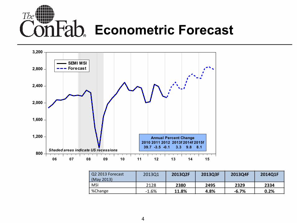
Econometric Forecast
800
1,200
1,600
2,000
2,400
2,800
3,200
06 07 08 09 10 11 12 13 14 15
SEMI MSIForecast
Shaded areas indicate US recessions
Annual Percent Change2010 2011 2012 2013f 2014f 2015f
39.7 -3.5 -0.1 3.3 9.8 8.1
Q2 2013 Forecast (May 2013)
2013Q1 2013Q2F 2013Q3F 2013Q4F 2014Q1F
MSI 2128 2380 2495 2329 2334 %Change -‐1.6% 11.8% 4.8% -‐6.7% 0.2%
5
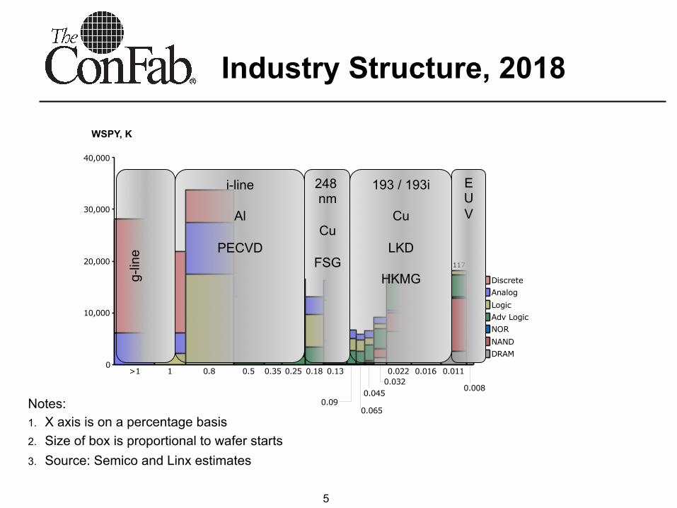
Industry Structure, 2018
0
10,000
20,000
30,000
40,000
>1 1 0.8 0.5 0.35 0.25 0.18 0.13 0.022 0.016
20,826
0.011
18,117
0.090.065
0.0450.032
0.008
DRAMNANDNORAdv LogicLogicAnalogDiscrete
Notes: 1. X axis is on a percentage basis 2. Size of box is proportional to wafer starts 3. Source: Semico and Linx estimates
WSPY, K g-
line
i-line Al
PECVD
248 nm
Cu
FSG
193 / 193i
Cu
LKD
HKMG
EUV
6
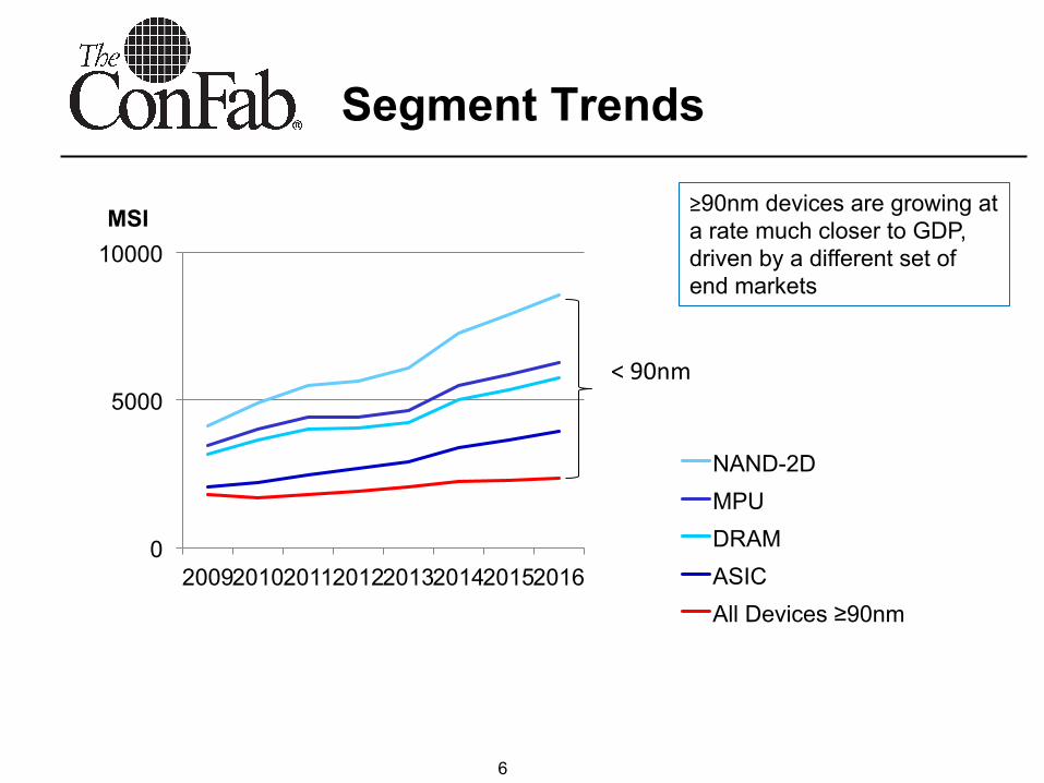
Segment Trends
0
5000
10000
2009 2010 2011 2012 2013 2014 2015 2016
MSI
NAND-2D MPU DRAM ASIC All Devices ≥90nm
< 90nm
≥90nm devices are growing at a rate much closer to GDP, driven by a different set of end markets
7
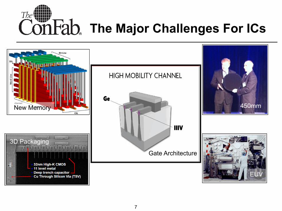
The Major Challenges For ICs
3D Packaging
450mm
Gate Architecture
EUV
New Memory
8
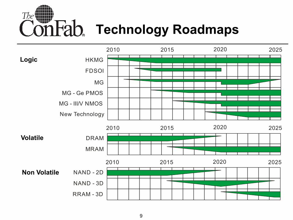
q Logic n Planar scaling is at an end n Move to fully depleted devices with FDSOI or MG n Migrate to new materials, Ge - PMOS, III/V – NMOS channels n New devices - tunnel FETs, nanowires, gate all around - in the long term
q Volatile memory n DRAM capacitor scaling challenges n MRAM is coming is sooner than previously expected
q Non-volatile memory n NAND 2D to 3D transition n Long term RRAM n PCRAM can’t meet the density of NAND but will find applications
replacing NOR and as storage class memory
Device Challenges
9
Technology Roadmaps 2010
HKMG
FDSOI
MG
MG - Ge PMOS
MG - III/V NMOS
New Technology
2015 2020 2025
2010
DRAM
MRAM
2015 2020 2025
2010
NAND - 2D
RRAM - 3D
NAND - 3D
2015 2020 2025
Logic
Volatile
Non Volatile
10
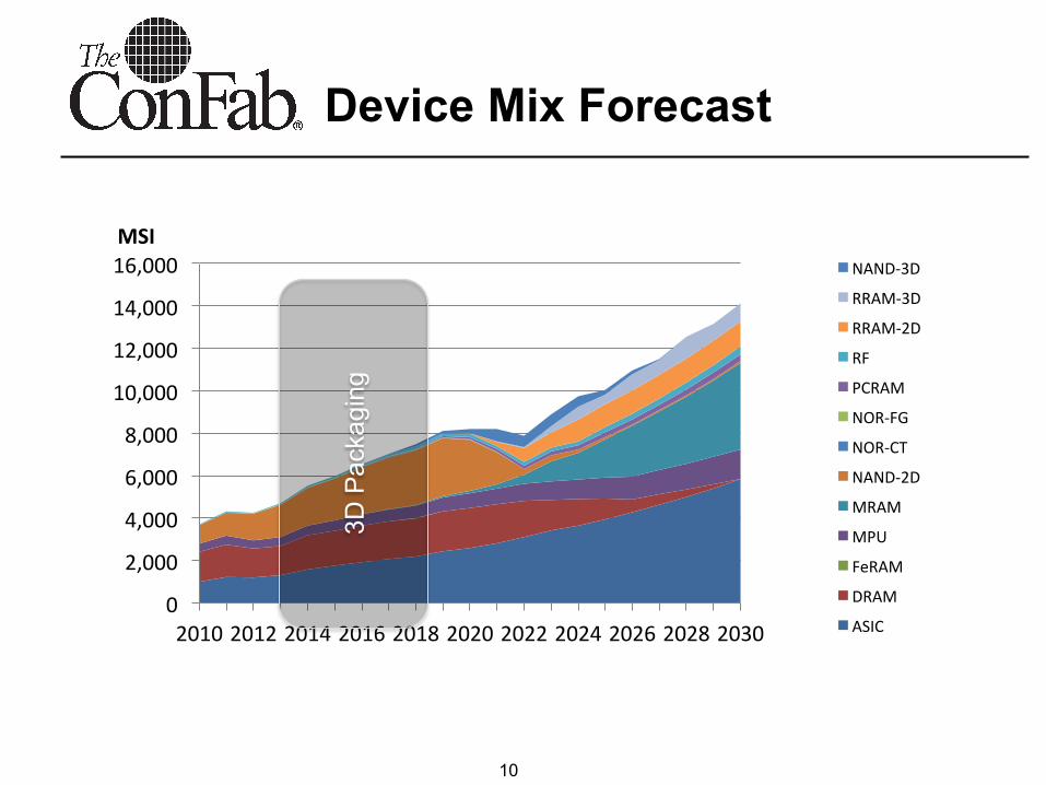
Device Mix Forecast
0
2,000
4,000
6,000
8,000
10,000
12,000
14,000
16,000
2010 2012 2014 2016 2018 2020 2022 2024 2026 2028 2030
MSI NAND-‐3D
RRAM-‐3D
RRAM-‐2D
RF
PCRAM
NOR-‐FG
NOR-‐CT
NAND-‐2D
MRAM
MPU
FeRAM
DRAM
ASIC
3D P
acka
ging
11
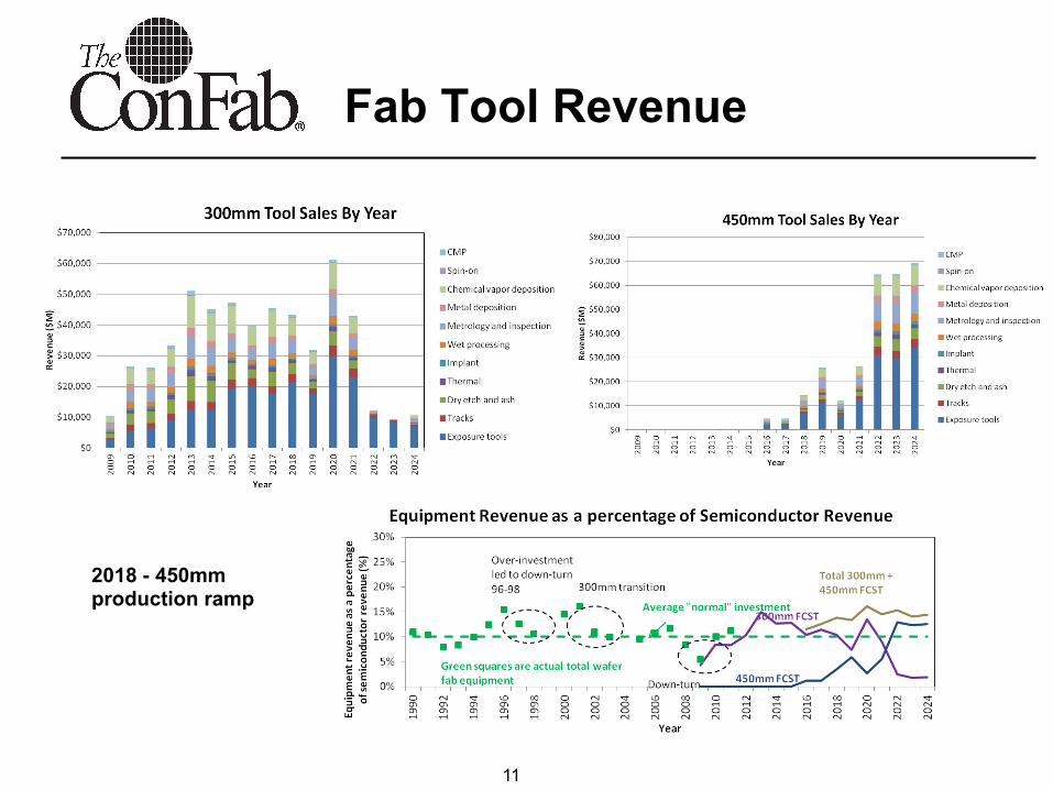
2018 - 450mm production ramp
Fab Tool Revenue
12
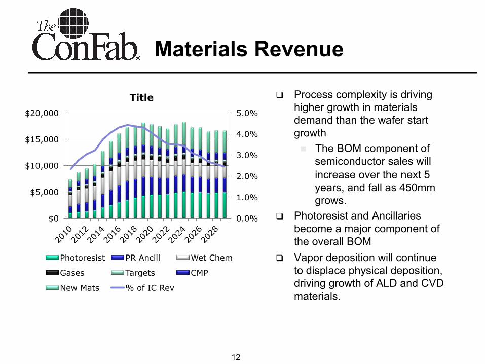
Materials Revenue
q Process complexity is driving higher growth in materials demand than the wafer start growth n The BOM component of
semiconductor sales will increase over the next 5 years, and fall as 450mm grows.
q Photoresist and Ancillaries become a major component of the overall BOM
q Vapor deposition will continue to displace physical deposition, driving growth of ALD and CVD materials.
0.0%
1.0%
2.0%
3.0%
4.0%
5.0%
$0
$5,000
$10,000
$15,000
$20,000
Title
Photoresist PR Ancill Wet Chem
Gases Targets CMP
New Mats % of IC Rev
13
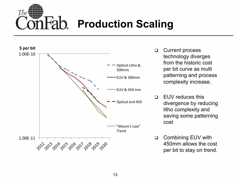
Production Scaling
q Current process technology diverges from the historic cost per bit curve as multi patterning and process complexity increase.
q EUV reduces this divergence by reducing litho complexity and saving some patterning cost
q Combining EUV with 450mm allows the cost per bit to stay on trend.
1.00E-‐11
1.00E-‐10
1.00E-‐09
$ per bit
OpOcal Litho & 300mm
EUV & 300mm
EUV & 450 mm
OpOcal and 450
Minimum
"Moore's Law" Trend
14
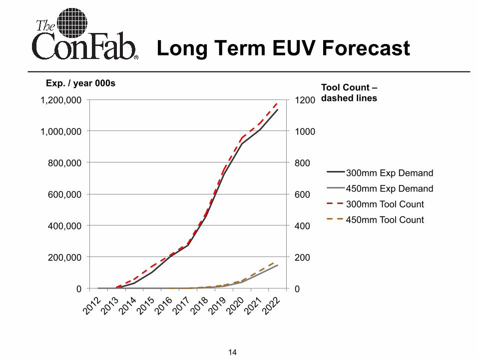
Long Term EUV Forecast
0
200
400
600
800
1000
1200
0
200,000
400,000
600,000
800,000
1,000,000
1,200,000 Tool Count – dashed lines
Exp. / year 000s
300mm Exp Demand
450mm Exp Demand
300mm Tool Count
450mm Tool Count
15
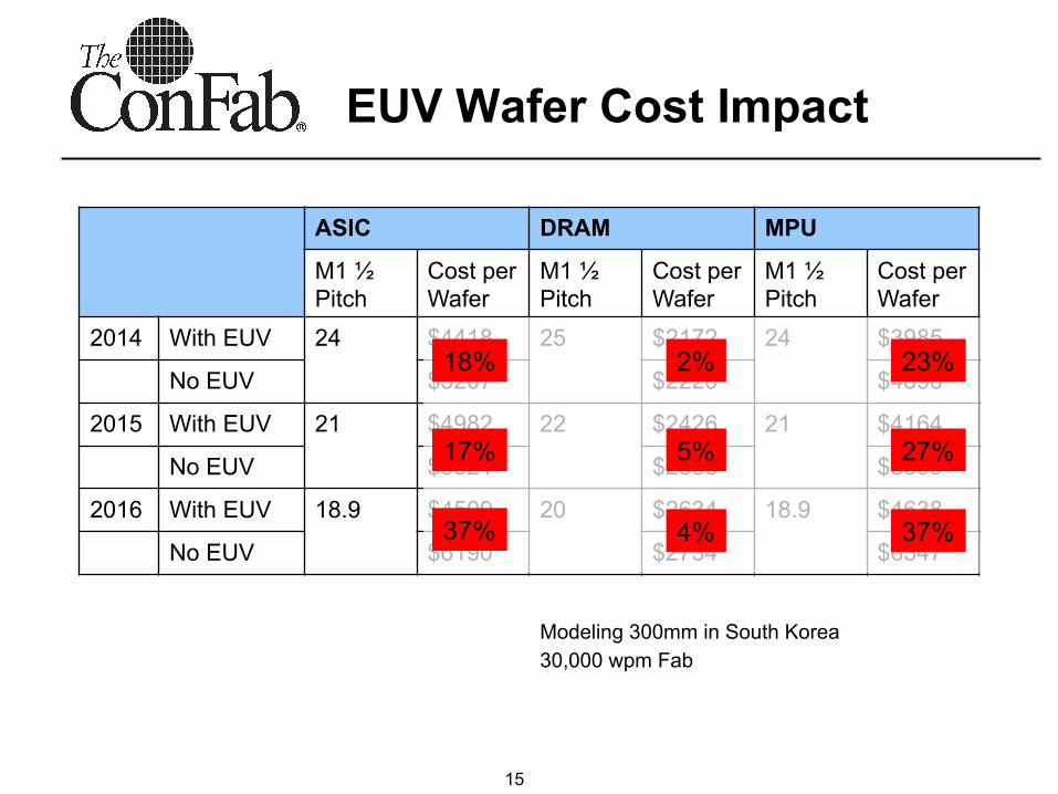
EUV Wafer Cost Impact
ASIC DRAM MPU
M1 ½ Pitch
Cost per Wafer
M1 ½ Pitch
Cost per Wafer
M1 ½ Pitch
Cost per Wafer
2014 With EUV 24 $4418 25 $2172 24 $3985
No EUV $5207 $2220 $4890
2015 With EUV 21 $4982 22 $2426 21 $4164
No EUV $5821 $2538 $5359
2016 With EUV 18.9 $4509 20 $2634 18.9 $4638
No EUV $6190 $2734 $6347
Modeling 300mm in South Korea 30,000 wpm Fab
18%
17%
37%
2%
5%
4%
23%
27%
37%
16
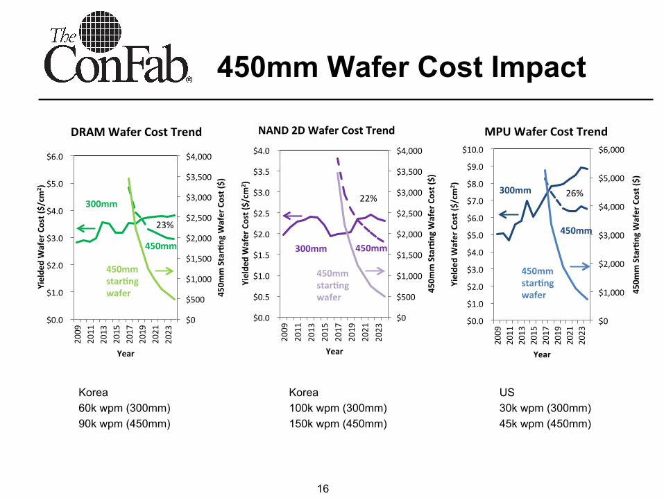
450mm Wafer Cost Impact
$0
$500
$1,000
$1,500
$2,000
$2,500
$3,000
$3,500
$4,000
$0.0
$1.0
$2.0
$3.0
$4.0
$5.0
$6.0
2009
2011
2013
2015
2017
2019
2021
2023
450m
m Star=ng W
afer Cost ($)
Yielde
d Wafer Cost ($/cm
2 )
Year
DRAM Wafer Cost Trend
300mm
450mm
23%
450mm star=ng wafer
$0
$500
$1,000
$1,500
$2,000
$2,500
$3,000
$3,500
$4,000
$0.0
$0.5
$1.0
$1.5
$2.0
$2.5
$3.0
$3.5
$4.0
2009
2011
2013
2015
2017
2019
2021
2023
450m
m Star=ng W
afer Cost ($)
Yielde
d Wafer Cost ($/cm
2 )
Year
NAND 2D Wafer Cost Trend
300mm 450mm
22%
450mm star=ng wafer
$0
$1,000
$2,000
$3,000
$4,000
$5,000
$6,000
$0.0
$1.0
$2.0
$3.0
$4.0
$5.0
$6.0
$7.0
$8.0
$9.0
$10.0
2009
2011
2013
2015
2017
2019
2021
2023
450m
m Star=ng W
afer Cost ($)
Yielde
d Wafer Cost ($/cm
2 )
Year
MPU Wafer Cost Trend
300mm
450mm
26%
450mm star=ng wafer
Korea 60k wpm (300mm) 90k wpm (450mm)
Korea 100k wpm (300mm) 150k wpm (450mm)
US 30k wpm (300mm) 45k wpm (450mm)
17
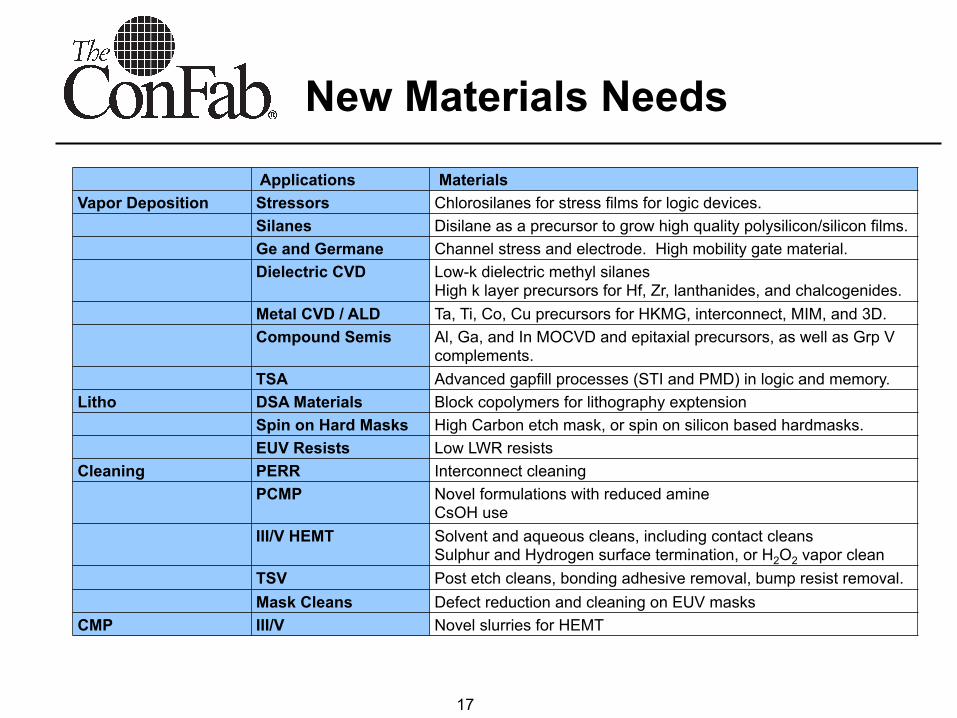
New Materials Needs
Applications Materials Vapor Deposition Stressors Chlorosilanes for stress films for logic devices.
Silanes Disilane as a precursor to grow high quality polysilicon/silicon films. Ge and Germane Channel stress and electrode. High mobility gate material. Dielectric CVD
Low-k dielectric methyl silanes High k layer precursors for Hf, Zr, lanthanides, and chalcogenides.
Metal CVD / ALD Ta, Ti, Co, Cu precursors for HKMG, interconnect, MIM, and 3D. Compound Semis Al, Ga, and In MOCVD and epitaxial precursors, as well as Grp V
complements. TSA Advanced gapfill processes (STI and PMD) in logic and memory.
Litho DSA Materials Block copolymers for lithography exptension Spin on Hard Masks High Carbon etch mask, or spin on silicon based hardmasks. EUV Resists Low LWR resists
Cleaning PERR Interconnect cleaning PCMP Novel formulations with reduced amine
CsOH use III/V HEMT Solvent and aqueous cleans, including contact cleans
Sulphur and Hydrogen surface termination, or H2O2 vapor clean TSV Post etch cleans, bonding adhesive removal, bump resist removal. Mask Cleans Defect reduction and cleaning on EUV masks
CMP III/V Novel slurries for HEMT
18
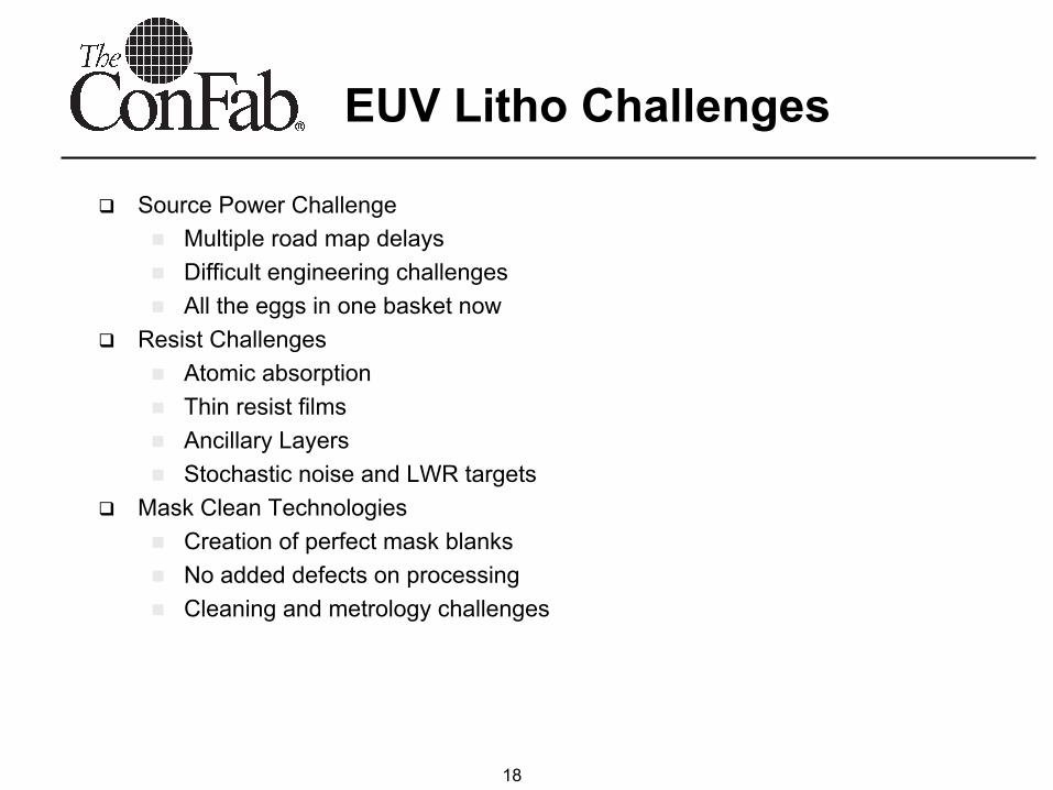
EUV Litho Challenges
q Source Power Challenge n Multiple road map delays n Difficult engineering challenges n All the eggs in one basket now
q Resist Challenges n Atomic absorption n Thin resist films n Ancillary Layers n Stochastic noise and LWR targets
q Mask Clean Technologies n Creation of perfect mask blanks n No added defects on processing n Cleaning and metrology challenges
19
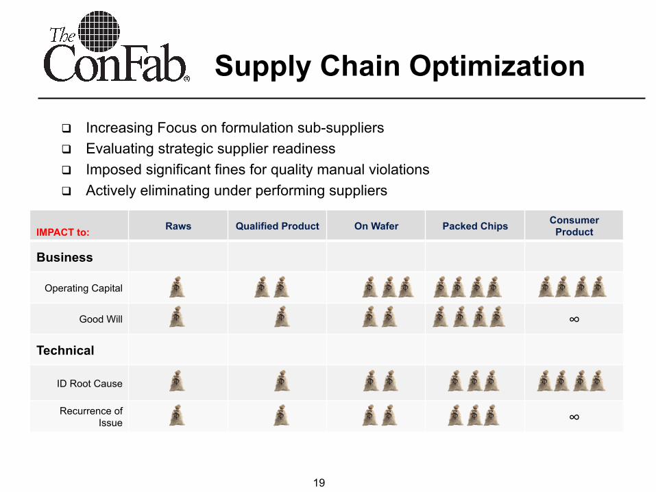
Supply Chain Optimization
q Increasing Focus on formulation sub-suppliers q Evaluating strategic supplier readiness q Imposed significant fines for quality manual violations q Actively eliminating under performing suppliers
IMPACT to: Raws Qualified Product On Wafer Packed Chips Consumer Product
Business
Operating Capital
Good Will ∞
Technical
ID Root Cause
Recurrence of Issue ∞
20
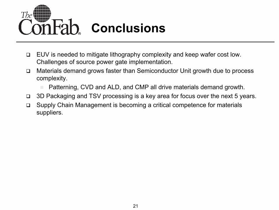
Conclusions
q Growth returns in 2013, but is moderate for the medium term. n Overall market growth is reducing.
q A high growth potential remains in advanced segments which will require specialty materials. n This is offset by significant R&D requirements. n HKMG, FinFETs, FDSOI, 3D-NAND and STT-MRAM development
programs are already well advanced, although challenges remain at 22nm and below.
q More Moore has significant implications for both equipment and materials suppliers. n 450mm is driven by fab economics. Prepare for deployment over the next 5
years. n 450mm will probably slow materials market volume growth, but require
advanced materials.
21
Conclusions
q EUV is needed to mitigate lithography complexity and keep wafer cost low. Challenges of source power gate implementation.
q Materials demand grows faster than Semiconductor Unit growth due to process complexity. n Patterning, CVD and ALD, and CMP all drive materials demand growth.
q 3D Packaging and TSV processing is a key area for focus over the next 5 years. q Supply Chain Management is becoming a critical competence for materials
suppliers.
22
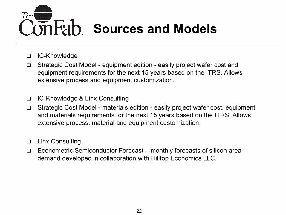
Sources and Models
q IC-Knowledge q Strategic Cost Model - equipment edition - easily project wafer cost and
equipment requirements for the next 15 years based on the ITRS. Allows extensive process and equipment customization.
q IC-Knowledge & Linx Consulting q Strategic Cost Model - materials edition - easily project wafer cost, equipment
and materials requirements for the next 15 years based on the ITRS. Allows extensive process, material and equipment customization.
q Linx Consulting q Econometric Semiconductor Forecast – monthly forecasts of silicon area
demand developed in collaboration with Hilltop Economics LLC.
23
Contacts
PO Box 384 Mendon MA, 01756 [email protected] (617) 273 8837 PO Box 20 Georgetown, MA 01833 [email protected] Px: (978) 352 - 7610 Fx: (978) 352 - 3870