theory and modelling of functional materials800747/fulltext01.pdf · computational physics, ......
TRANSCRIPT
ACTAUNIVERSITATIS
UPSALIENSISUPPSALA
2015
Digital Comprehensive Summaries of Uppsala Dissertationsfrom the Faculty of Science and Technology 1247
Theory and Modelling ofFunctional Materials
VANCHO KOCEVSKI
ISSN 1651-6214ISBN 978-91-554-9231-1urn:nbn:se:uu:diva-248513

Dissertation presented at Uppsala University to be publicly examined in Å10132 (Häggsalen),Ångström Laboratory, Lägerhydddsvägen 1, Uppsala, Wednesday, 27 May 2015 at 13:30 forthe degree of Doctor of Philosophy. The examination will be conducted in English. Facultyexaminer: Christophe Delerue (ISEN (Institut Supérieur de l'Électronique et du Numérique)).
AbstractKocevski, V. 2015. Theory and Modelling of Functional Materials. Digital ComprehensiveSummaries of Uppsala Dissertations from the Faculty of Science and Technology 1247. 93 pp.Uppsala: Acta Universitatis Upsaliensis. ISBN 978-91-554-9231-1.
The diverse field of material research has been steadily expanding with a great help fromcomputational physics, especially in the investigation of the fundamental properties of materials.This has driven the computational physics to become one of the main branches of physics,allowing for density functional theory (DFT) to develop as one of the cornerstones of materialresearch. Nowdays, DFT is the method of choice in a great variety of studies, from fundamentalproperties, to materials modelling and searching for new materials. In this thesis, DFT isemployed for the study of a small part of this vast pool of applications. Specifically, themicroscopic characteristics of Zn1-xCdxS alloys are studied by looking into the evolution of thelocal structure. In addition, the way to model the growth of graphene on Fe(110) surface isdiscussed. The structural stability of silicon nanocrystals with various shapes is analysed indetail, as well.
DFT is further used in studying different properties of semiconductor nanocrystals. Thesize evolution of the character of the band gap in silicon nanocrystals is investigated interms of changes in the character of the states around the band gap. The influence of varioussurface impurities on the band gap, as well as on the electronic and optical properties ofsilicon nanocrystals is further studied. In addition, the future use of silicon nanocrystals inphotovoltaic devices is examined by studying the band alignment and the charge densitiesof silicon nanocrystals embedded in a silicon carbide matrix. Furthermore, the electronic andoptical properties of different semiconductor nanocrystals is also investigated. In the case ofthe CdSe/CdS and CdS/ZnS core-shell nanocrystals the influence of the nanocrystal size anddifferent structural models on their properties is analysed. For silicon nanocrystal capped withorganic ligands, the changes in the optical properties and lifetimes is thoroughly examined withchanges in the type of organic ligand.
Keywords: nanocrystals, graphene, alloys, density functional theory, optical properties,electronic properties, core-shell structures, semiconductors
Vancho Kocevski, Department of Physics and Astronomy, Materials Theory, Box 516, UppsalaUniversity, SE-751 20 Uppsala, Sweden.
© Vancho Kocevski 2015
ISSN 1651-6214ISBN 978-91-554-9231-1urn:nbn:se:uu:diva-248513 (http://urn.kb.se/resolve?urn=urn:nbn:se:uu:diva-248513)

Dedicated to my family

List of papers
This thesis is based on the following papers, which are referred to in the text
by their Roman numerals.
I Transition between direct and indirect band gap in siliconnanocrystalsV. Kocevski, O. Eriksson, J. Rusz
Physical Review B 87, 245401 (2013).
II Size dependence of the stability, electronic structure, and opticalproperties of silicon nanocrystals with various surface impuritiesV. Kocevski, O. Eriksson, J. Rusz
Physical Review B 91, 125402 (2015).
III Band alignment switching and the interaction betweenneighbouring silicon nanocrystals embedded in a SiC matrixV. Kocevski, O. Eriksson, J. Rusz
Physical Review B, accepted.
IV First-principles study of the influence of different interfaces andcore types on the properties of CdSe/CdS core-shell nanocrystalV. Kocevski, J. Rusz, O. Eriksson, D. D. Sarma
submitted.
V Influence of dimensionality and interface type on optical andelectronic properties of CdS/ZnS core-shell nanocrystals: Afirst-principles studyV. Kocevski, O. Eriksson, C. Gerard, D. D. Sarma, J. Rusz
submitted.
VI Electronic and optical properties of silicon nanocrystals cappedwith organic ligands studied using first-principles theoryV. Kocevski
manuscript.
VII Formation and structure of graphene waves on Fe(110)N. A. Vinogradov, A. A. Zakharov, V. Kocevski, J. Rusz, K. A.
Simonov, O. Eriksson, A. Mikkelsen, E. Lundgren, A. S. Vinogradov,
N. Mårtensson, A. B. Preobrajenski
Physical Review Letters 109, 026101 (2012).

VIII Microscopic description of the evolution of the local structure andan evaluation of the chemical pressure concept in a solid solutionS. Mukherjee, A. Nag, V. Kocevski, P. K. Santra, M. Balasubramanian,
S. Chattopadhyay, T. Shibata, F. Schaefers, J. Rusz, C. Gerard, O.
Eriksson, C. U. Segre, D. D. Sarma
Physical Review B 89, 224105 (2014).
Reprints were made with permission from the publishers.
The following papers are co-authored by me, but not included in the thesis
• Quantitative characterization of nanoscale polycrystalline magnetswith electron magnetic circular dichroismS. Muto, J. Rusz, K. Tatsumi, R. Adam, S. Arai, V. Kocevski, P. M.
Oppeneer, D. E. Bürgler, C. M. Schneider
Nature Communication 5, 3138 (2014).
Comments on my participation
My participation in Papers I, II, III, IV, V, VI and VIII is in all three parts,
planning the research, calculations and writing the manuscript. The experi-
mental part in Paper VIII is performed by the group of D.D. S. The projects in
Papers II, III and VI were designed by me. The experimental part in Paper VII
is performed by the group of N. A. V.
Contents
1 Introduction . . . . . . . . . . . . . . . . . . . . . . . . . . . . . . . . . . . . . . . . . . . . . . . . . . . . . . . . . . . . . . . . . . . . . . . . . . . . . . . . . . . . . . . . . . . . . . . . 13
2 Theoretical background . . . . . . . . . . . . . . . . . . . . . . . . . . . . . . . . . . . . . . . . . . . . . . . . . . . . . . . . . . . . . . . . . . . . . . . . . . . . . 19
2.1 Many body problem . . . . . . . . . . . . . . . . . . . . . . . . . . . . . . . . . . . . . . . . . . . . . . . . . . . . . . . . . . . . . . . . . . . . . . . 19
2.2 Thomas-Fermi-Dirac approximation . . . . . . . . . . . . . . . . . . . . . . . . . . . . . . . . . . . . . . . . . . . . 20
2.3 Density functional theory . . . . . . . . . . . . . . . . . . . . . . . . . . . . . . . . . . . . . . . . . . . . . . . . . . . . . . . . . . . . . . 21
2.3.1 Hohenberg-Kohn theorems . . . . . . . . . . . . . . . . . . . . . . . . . . . . . . . . . . . . . . . . . . . . . 21
2.3.2 Kohn-Sham equation . . . . . . . . . . . . . . . . . . . . . . . . . . . . . . . . . . . . . . . . . . . . . . . . . . . . . . . 22
2.4 Approximations to the exchange-correlation functional . . . . . . . . . . . . . 23
2.4.1 Local Density Approximation . . . . . . . . . . . . . . . . . . . . . . . . . . . . . . . . . . . . . . . . 23
2.4.2 Generalised-Gradient Approximation . . . . . . . . . . . . . . . . . . . . . . . . . . . . 24
2.5 Computations on solids . . . . . . . . . . . . . . . . . . . . . . . . . . . . . . . . . . . . . . . . . . . . . . . . . . . . . . . . . . . . . . . . . . 24
2.6 Pseudopotentials . . . . . . . . . . . . . . . . . . . . . . . . . . . . . . . . . . . . . . . . . . . . . . . . . . . . . . . . . . . . . . . . . . . . . . . . . . . . . 25
2.7 Basis set . . . . . . . . . . . . . . . . . . . . . . . . . . . . . . . . . . . . . . . . . . . . . . . . . . . . . . . . . . . . . . . . . . . . . . . . . . . . . . . . . . . . . . . . . . 27
3 SIESTA – our choice of DFT implementation . . . . . . . . . . . . . . . . . . . . . . . . . . . . . . . . . . . . . . . . . . 28
3.1 Norm-conserving pseudopotentials . . . . . . . . . . . . . . . . . . . . . . . . . . . . . . . . . . . . . . . . . . . . . . 28
3.2 LCAO basis set . . . . . . . . . . . . . . . . . . . . . . . . . . . . . . . . . . . . . . . . . . . . . . . . . . . . . . . . . . . . . . . . . . . . . . . . . . . . . . . 30
3.2.1 Single and multiple zeta basis sets . . . . . . . . . . . . . . . . . . . . . . . . . . . . . . . . 31
3.2.2 Polarized basis sets . . . . . . . . . . . . . . . . . . . . . . . . . . . . . . . . . . . . . . . . . . . . . . . . . . . . . . . . . . 31
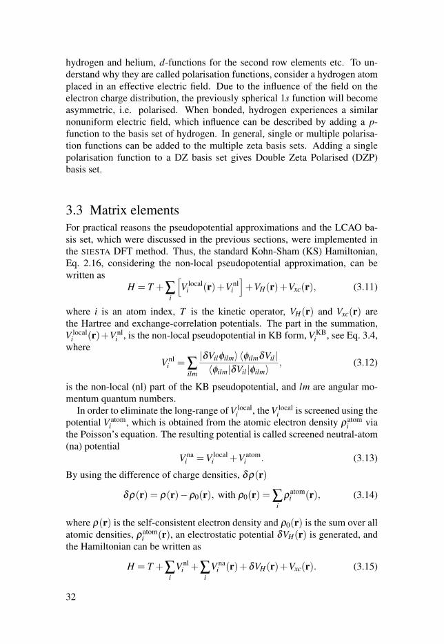
3.3 Matrix elements . . . . . . . . . . . . . . . . . . . . . . . . . . . . . . . . . . . . . . . . . . . . . . . . . . . . . . . . . . . . . . . . . . . . . . . . . . . . . . 32
3.4 Total energy . . . . . . . . . . . . . . . . . . . . . . . . . . . . . . . . . . . . . . . . . . . . . . . . . . . . . . . . . . . . . . . . . . . . . . . . . . . . . . . . . . . . 33
4 Quantum confinement regime in silicon nanocrystals . . . . . . . . . . . . . . . . . . . . . . . . . . . . 37
4.1 Hydrogenated silicon nanocrystals . . . . . . . . . . . . . . . . . . . . . . . . . . . . . . . . . . . . . . . . . . . . . . . 38
4.2 Influence of the surface impurities . . . . . . . . . . . . . . . . . . . . . . . . . . . . . . . . . . . . . . . . . . . . . . . . 41
4.3 Embedded silicon nanocrystals . . . . . . . . . . . . . . . . . . . . . . . . . . . . . . . . . . . . . . . . . . . . . . . . . . . . . 45
5 Semiconductor nanocrystals – significance of the interface and the
capping of the surface . . . . . . . . . . . . . . . . . . . . . . . . . . . . . . . . . . . . . . . . . . . . . . . . . . . . . . . . . . . . . . . . . . . . . . . . . . . . . . . 49
5.1 Recombination processes in semiconductor nanocrystals . . . . . . . . . . . 51
5.1.1 Radiative recombination . . . . . . . . . . . . . . . . . . . . . . . . . . . . . . . . . . . . . . . . . . . . . . . . . 51
5.1.2 Non-radiative recombination . . . . . . . . . . . . . . . . . . . . . . . . . . . . . . . . . . . . . . . . . . 53
5.1.3 Auger recombination . . . . . . . . . . . . . . . . . . . . . . . . . . . . . . . . . . . . . . . . . . . . . . . . . . . . . . . 54
5.2 CdSe/CdS core-shell NCs . . . . . . . . . . . . . . . . . . . . . . . . . . . . . . . . . . . . . . . . . . . . . . . . . . . . . . . . . . . . . . 54
5.3 CdS/ZnS core-shell NCs . . . . . . . . . . . . . . . . . . . . . . . . . . . . . . . . . . . . . . . . . . . . . . . . . . . . . . . . . . . . . . . . 58
5.4 Comparison between CdSe/CdS and CdS/ZnS core-shell NCs . . 61
5.5 Si nanocrystals capped with organic ligands . . . . . . . . . . . . . . . . . . . . . . . . . . . . . . . . 65

6 Modelling of nanocrystals, surfaces and bulk materials . . . . . . . . . . . . . . . . . . . . . . . . . 70
6.1 Ripples of graphene on Fe(110) surface . . . . . . . . . . . . . . . . . . . . . . . . . . . . . . . . . . . . . . . 70
6.2 Silicon nanocrystals with various shapes . . . . . . . . . . . . . . . . . . . . . . . . . . . . . . . . . . . . . 71
6.3 Evolution of the local structure in solid solutions . . . . . . . . . . . . . . . . . . . . . . . . 74
7 Summary and outlook . . . . . . . . . . . . . . . . . . . . . . . . . . . . . . . . . . . . . . . . . . . . . . . . . . . . . . . . . . . . . . . . . . . . . . . . . . . . . . . 81
8 Sammanfattning . . . . . . . . . . . . . . . . . . . . . . . . . . . . . . . . . . . . . . . . . . . . . . . . . . . . . . . . . . . . . . . . . . . . . . . . . . . . . . . . . . . . . . . . . 84
Acknowledgments . . . . . . . . . . . . . . . . . . . . . . . . . . . . . . . . . . . . . . . . . . . . . . . . . . . . . . . . . . . . . . . . . . . . . . . . . . . . . . . . . . . . . . . . . . . 87
References . . . . . . . . . . . . . . . . . . . . . . . . . . . . . . . . . . . . . . . . . . . . . . . . . . . . . . . . . . . . . . . . . . . . . . . . . . . . . . . . . . . . . . . . . . . . . . . . . . . . . . . . 89
Preface
Greetings dear reader.
The quest for the paramount knowledge, referred to as a doctoral degree,
started approximately four and a half years ago, when Dr. Ján Rusz decided
to give a change to the particular candidate to pursuit this knowledge. Both
of them begun the journey not knowing what difficulties and challenges might
emerge on the path to the ultimate goal. Any obstacle that the science pre-
sented them with was tackled head on, disagreements were overcome, and the
laziness (from the student side) was from time to time suppressed. This thesis
is the outcome of their mutual productive work, with tremendous help from
the second supervisor Prof. Olle Eriksson.
As the title of this thesis suggests, the employment of theoretical methods in
studying fundamental properties and modelling of various materials is going to
be presented. For smoother following of the main ideas, the content is divided
in two parts, and an additional part for the papers.
The first part provides a general introduction to the research field, the topic of
the thesis, and the methods employed in studying the particular systems. This
could be used as a guidance for easier understanding of the second part and
the included papers.
The overview of the most significant results are discussed in the second part.
This part is divided in three chapters, in which studies with similar objectives
and of related systems are systematised.
I sincerely hope that you are going to enjoy reading this thesis.
Uppsala, April 2015
Vancho Kocevski


FUNDAMENTALS


1. Introduction
The interest in the properties of materials dates back to the dawn of humanity.
Our early ancestors realised that using particular stones for a given purpose
provided them with an advantage over the other species. This enabled the
humans to begin their mastery over the land and resources. Later came the
production of more durable tools, with the discovery of iron and bronze, which
further cemented the importance of striving to find better materials. At the
same time started the search of producing better pottery, finer colours and
glazes. Furthermore, the jewellery was becoming a lucrative trade, which
relied on the jewellery makers’ extensive knowledge of the various precious
materials used in the production. Primitive as they are, these can be regarded
as the earliest examples of research in materials.
The research started gathering momentum during the Middle Ages, espe-
cially in the work of the alchemists. Although their goals were far reaching,
their methods of experimenting and the findings that they provided laid the
foundation of many sciences, including the basic principles of material re-
search. Things evolved even further in the New Age, when the understanding
of the natural world started to progress. The Industrial Revolution brought
with it the manufacturing of abundance of other useful products and the re-
quirement for new and better materials. This in turn conceived the importance
for investment in materials advances and the research in this field. The newly
formed scientist were intrigued by the various features of the materials, which
could not be explained using the common knowledge of that time. Particularly
valuable was the research in electrical currents and magnetism done by H. A.
Lorentz [1] and P. Zeeman [2], respectively. Furthermore, the invention of
the cathode-ray tube by K. F. Braun [3] and J. J. Thomson’s discovery of the
electron [4] marked the start of a new scientific era.
With the discovery of the atomic nucleus by E. Rutherford, which came
from the interpretation of the H. Geiger and E. Marsden experiment [5], the
need of modelling the atomic inner structure was realised. The most ground-
breaking atomic model was proposed by N. Bohr [6–8], who introduced the
idea of stationary orbits defined by quantised angular momentum, and the
possibility of transitions between these orbits. The idea of quantisation was
actually first presented by M. Planck in his ad hoc hypothesis [9] that the elec-
tronic oscillations are quantised in multiples of h – the Planck’s constant. This
hypothesis was later extended to the quantisation of the electromagnetic radi-
ation by A. Einstein [10]. In addition to these hypotheses, O. Stern and W.
Gerlach provided the first evidence of the quantisation of the spin [11–13].
13

The introduction of quantisation of energy, angular momentum and the spin,
set the stepping-stone for the new physical theory explaining the fundamental
behaviour of microscopic particles – the quantum mechanics.
Following these new and exiting findings, the development of formula-
tion of quantum mechanics was steadily moving forward. Almost simulta-
neously, M. Born, P. Jordan and W. Heisenberg [14–16], on one hand, and E.
Schrödinger [17–20] on the other, developed the so-called matrix mechanics
and the wave mechanics, respectively. In Schrödinger’s formulation, the quan-
tum system’s dynamics can be represented as a function of the kinetic and the
potential energy, given by the equation:
ih∂∂ t
ψ(r, t) =(− h2
2mΔ+V (r)
)ψ(r, t). (1.1)
where ψ(r, t) is a many-particle wavefunction, (− h2m Δ) is the kinetic and V (r)
is the potential energy. However, in these formulations of quantum mechanics
the spin is not included. To integrate the electron spin in the Schrödinger’s
equation, W. Pauli considered the many-particle wavefunction to be antisym-
metric [21]. Subsequently, Dirac formulated the relativistic quantum mechan-
ics [22, 23], which in principle can be employed to calculate almost any phe-
nomena dependent on the electronic structure of matter.
Immediately after the foundation of quantum mechanics was established
by the wave mechanics formulation, it was evident that properties of atoms,
molecules and solids could be obtained by solving the Schrödinger’s equation.
However, except for few limited cases, solving the Schrödinger’s equation an-
alytically is almost impossible, which prompt the implementation of approx-
imative ways of solving it. Among the first approximations, now considered
as the basic method, and introduced in order to deal with chemically bonded
systems, was the Hartree-Fock (HF) theory [24–26]. Although it works suffi-
ciently well for simple systems, the HF theory has a major drawback arising
from the employment of single-determinant form of the wavefunction, thus
neglecting the electron correlations. This problem was dealt with by treating
the electron correlations as perturbation of the HF wavefunction, providing the
basics of the many-body perturbation theory (MBPT) [27–29].
A decade after the MBPT was proposed, two distinct methods for solving
the many-electron problem were developed almost simultaneously. The first
one, Quantum Monte Carlo (QMC), which comprises several different tech-
niques, is based on numerical Monte Carlo integration for solving the many-
electron problem. The most widely used QMC techniques are the variational
Monte Carlo [30] and the diffusion Monte Carlo [31–33]. The QMC is very
accurate, but the calculations are time-consuming and therefore currently it
is used only for studying small systems. The second method is density func-
tional theory (DFT) [34, 35], which postulates that the properties of a system
are dependent on the electron density, via an exchange-correlation functional,
14

and the many-body problem is reduced to finding this electron density. Know-
ing the exact form of the exchange-correlation functional can yield accurate
results. However, the exact form of the exchange-correlation functional is
beyond current knowledge and many approximations have been instead intro-
duced. In spite of its approximative nature, to date DFT is the most widely
used computational method for studying materials. This seeming contradic-
tion will be explained in the rest of this chapter by detailing the significance
of DFT in material research. The basics of DFT are summarised in Sec. 2.3.
It is difficult to imagine the modern material research without the input pro-
vided from DFT. It not only gives fundamental understanding of the processes
on atomistic level, it is also essential in investigating and predicting the prop-
erties of materials. There are various aspects of DFT that contribute to this
increased importance in material research, compared to other approximative
methods. One of the main advantages is the applicability of DFT in describing
various distinct classes of materials. More specifically, the experience gained
from studying one material can be easily employed for the study of any other.
Simple and intuitive, DFT also provides reliable results for different exper-
imentally accessible properties. The increased computational power and the
improved implementation of DFT in computational codes further expanded its
usability, especially for larger systems. In addition, the popularity of DFT has
increased with the introduction of standardised codes and open-source soft-
ware.
There are though number of shortcomings that should at this point be men-
tioned. First of all, as a ground-state theory DFT fails to predict excited states,
giving unreliable results when it comes to representing emission properties of
materials. In addition, the description of van der Waals interactions is incom-
plete, introducing errors when studying weakly bonded system. Electrons in
strongly correlated system are not correctly described by local density approx-
imation (LDA) of the exchange-correlation functional, which wrongly predicts
a metallic character of these materials. To solve this problem the LDA+U
approach has been developed, which is based on combining the Coulomb re-
pulsion U of narrow d- and f -bands with DFT description of extended states.
Moreover, despite the weaknesses, DFT serves as the foundation for further
more sophisticated calculations, termed ’post-DFT’ corrections. These meth-
ods are employed in order to improve the predictive power of DFT. For exam-
ple, using many-body perturbation theory, e.g. GW or BSE as an extension to
the ground-state DFT, gives more accurate description of the emission proper-
ties of materials and their band structures.
Interestingly, the applicability of DFT is wide spread, ranging from studies
in nanoscience and nanoengineering, magnetics, elastic and catalytic proper-
ties, to biomaterials, geoscience and new emerging materials. Nowdays, a
great deal of attention has also been given to the computational spectroscopy
and to the study of transport properties in molecular electronics. The possible
implementation of the exceptional properties of graphene in everyday devices
15

has been heavily investigated by relying on the predictive power of DFT. The
DFT is also largely utilised in the investigation of electronic and optical prop-
erties of nanocrystals, providing explanations for various experimentally ob-
served phenomena. Moreover, when researching for materials with particular
physical properties, DFT can give reliable data on elastic properties, defect
formation and dislocation behaviour. In the search for new and improved rare-
earth free permanent magnets, DFT is not only important in supporting the
experimental results, but also in predicting favourable magnetic properties of
novel materials.
DFT has proven invaluable also in the study of solid catalysts, especially be-
cause it provides an information which is difficult to obtain by experiments. It
gives an atomic-scale picture of the way catalysts work by describing the tran-
sition states at the surface, which constitute the base for reactivity models. The
predictive power of DFT can be also harnessed in areas where experimental
results do not exist or are difficult to obtain. It is of great importance in sim-
ulating the structural changes in the Earth’s core and mantle with changes in
pressure and temperature, which is otherwise close to impossible to reproduce
in a laboratory. In addition, DFT is the main tool of the emerging research area
known as the high-troughput computational materials design used in screen-
ing for new materials. The method is based on gathering thermodynamic and
electronic properties data for a large number of systems, and combining it with
data mining to find materials with desired properties. Have in mind that beside
these examples, there are many other instances where DFT helps in explaining
and predicting fundamental properties of matter, but have been left out from
this list.
One of the main reason for the widespread use of DFT in material research
comes from the implementation of efficient algorithms for solving the quan-
tum mechanical equations. The variety of codes in which DFT is implemented
employ different ways of solving the Kohn-Sham equations, and have various
choices of basis sets, potentials and exchange-correlation functionals. Choos-
ing a particular code mainly depends on the size of the studied system and the
required level of accuracy of the obtained results. Currently, the most accu-
rate codes are based on all-electron approaches, including relativistic effects,
and a combination of plane waves with localised orbitals as basis set. How-
ever, the calculations performed using these codes are highly time consuming,
even with the considerable advancements in computational power. Therefore,
for large systems one resorts to using codes based on pseudopotentials and
localised basis sets, for which lower computational cost is required, but still
provide rather accurate results. This thesis centers around the usability of
DFT in modelling nanocrystals, surfaces and bulk material. Considering the
large size of the systems, a few thousands of atoms, we used the DFT codeSIESTA [36, 37], based on pseudopotentials and localised basis sets. Details
regarding the basic implementation of SIESTA are given in Chapter 3.
16

The research in nanostructured materials relies greatly on the capabilities
of DFT to provide explanations for the experimentally observed phenomena.
In various occasions DFT has managed to give deeper insight into the surface
reconstruction of nanomaterials, the effect of doping on their properties and
into the possibility of designing new and improved nanomaterials. Of great
importance is also the study of electronic and optical properties of nanocrystals
for future use in microelectronics. The usability of DFT in studying large
nanocrystals, with sizes closer to the experimentally analysed ones, however
was limited due to the efficiency of the existing DFT codes. A significant
boost to the large scale calculations came with the implementation of localised
basis sets and pseudopotentials, coupled with the ever-growing power of the
supercomputers. These improvements in computations enabled us to study the
optical and electronic properties of various nanocrystals with sizes comparable
to the experimental ones.
The great significance of producing nanocrystals for light emitting applica-
tions comes from exploiting the quantum confinement effect that they exhibit.
By confining the size of the nanocrystals, both the energy and the intensity of
the emitted light increase. Moreover, even nanocrystals made from indirect
band gap semiconductors, e.g. Si and Ge, in which the emission of light must
be coupled with a phonon, exhibit increased photoluminiscence. The abun-
dance of silicon and the easy way of producing silicon nanocrystals, together
with the high photoluminiscence, has sparked considerable interest in studying
the usability of silicon nanocrystals. The wide spread of experimental results
and the unexpected photoluminiscence of an indirect band gap semiconduc-
tor, has drawn the attention of theoreticians aimed to provide a detailed expla-
nation for these surprising results with the help of DFT. The realisation that
surface oxidation can significantly influence the photoluminiscence of silicon
nanocrystals, has risen even further the interest for using DFT in obtaining
fundamental understanding of the processes taking place in silicon nanocrys-
tals.
Although there exists studies that give an explanation of the experimentally
observed phenomena in hydrogenated [38] and oxygenated silicon nanocrys-
tals [39], they are based on the tight-binding model. To provide a more ac-
curate theoretical description of the processes occurring in these nanocrystals,
parameter-free DFT is preferably used. This was the main aim in our study of
silicon nanocrystals. We investigated the size evolution of the fundamental and
optical band gap in hydrogenated silicon nanocrystals, and nanocrystals with
various surface impurities. This was further extended to studying the changes
in the wavefunctions of the highest occupied (HOMO) and lowest unoccupied
(LUMO) eigenstate, with changes in the nanocrystal size and type of surface
impurity.
To suppress the oxidation of the silicon nanocrystals’ surface, the nanocrys-
tals are capped with organic ligands, which improves their photoluminiscence
properties. Moreover, different organic ligands can have distinct influence on
17

the photoluminiscence of the silicon nanocrystals. Understanding the changes
in the optical and electronic properties of silicon nanocrystals capped with dif-
ferent organic ligands, was also one of the objective of this thesis. Capping
the surface of the nanocrystals, to reduce the influence of surface effects and
improve their photoluminiscence, is not specific only for silicon nanocrystals.
II-VI semiconductor nanocrystals, for example, are frequently capped with
other semiconductor (forming core-shell nanocrystals) in order to suppress
the surface effects and enable manipulation of their properties for a specific
purpose. In addition, the photoluminiscence properties can be influenced by
changes in the structure of the core or the core-shell interface.
Of significant interest are the core-shell structures where both the electron
and hole are confined within the core of the nanocrystals, especially because of
their enhanced light emitting properties. Important representatives of this type
of systems are the CdSe/CdS and CdS/ZnS core-shell nanocrystals, which de-
spite the large number of experimental studies, has not been previously studied
using more accurate first-principles theory. Therefore, we set our objective in
demonstrating the size dependence and the influence of the different structural
models on the electronic and optical properties of these core-shell nanocrys-
tals. Furthermore, we relate the calculated radiative lifetimes and electron-
hole Coulomb interaction energies with experimentally observed quantities,
in order to show the differences in the properties of the two types of core-shell
nanocrystals and the properties related to the distinct structural models.
The improved properties of the semiconductors upon nanocrystal forma-
tion, can be also utilised in photovoltaic applications, but this is only applica-
ble if the nanocrystals are embedded in a host matrix. Among many semicon-
ductor nanocrystals, the silicon nanocrystals have triggered the highest interest
for producing new-generation solar cells. It is important, therefore, to find a
suitable host matrix, which gives high light conversion efficiency, by reducing
the recombination rates of the charge carrier and increasing their mobility. We
focused on the study on SiC as a host matrix, investigating the band alignment
between the silicon nanocrystal and the SiC matrix, which can provide valu-
able information regarding the recombination rates between the charge carri-
ers. In addition, we looked into the possibility of increasing charge transport
by having leakage between states.
In other parts of the thesis, collaborative studies with experiments are given,
showing the capability of DFT to reliably model the structure of bulk materi-
als, surfaces and nanocrystals. The investigation the Zn1-xCdxS ternary alloys,
aimed in providing more fundamental, microscopic understanding of the struc-
tural characteristics is presented. Modelling of the formation of graphene on
Fe(110) surface, with focus on the buckling effect, is also given. Considerable
attention in this thesis has been given to DFT study of silicon nanocrystals.
Hence, before performing detailed calculations of the electronic and optical
properties, we studied the stability of nanocrystals with various shapes.
18

2. Theoretical background
2.1 Many body problemFrom the basics of quantum mechanics follows that the properties of a system
can be obtained by solving a many body equation, which for non-relativistic
time-independent calculations is the Schrödinger equation:
Hψ(r1,r2, . . . ,R1,R2, . . .) = Eψ(r1,r2, . . . ,R1,R2, . . .), (2.1)
where ψ(r1,r2, . . . ,R1,R2, . . .) is the all electron wavefunction, which de-
pends on the position of the electrons, r, and the nuclei, R. H represents
the Hamiltonian of the interacting system, which can be expressed as:
H =− h2
2me∑
i∇2
i −∑I
h2
2mI∇2
I −∑i,I
ZIe2
|ri −RI |+
+1
2∑i�= j
e2
|ri − r j| +1
2∑I �=J
ZIZJe2
|RI −RJ| ,(2.2)
where me and mI are the mass of the ith electron and Ith nucleus, respectively,
and ZI is the atomic number of the Ith atom. The first and the second term are
respectively the kinetic energy of the electrons and the nuclei. The remaining
three terms are the potential energy from Coulomb interaction between elec-
tron and nucleus, electron and electron, and nucleus and nucleus, respectively.
However, as mentioned in the introduction, obtaining analytical solution of
the Schrödinger equation in this form is limited to a small number of systems,
and to broaden its applicability to every system, approximations need to be
implemented. The first approximation utilises the large mass difference be-
tween the nuclei and the electrons (nuclei are 3-5 orders of magnitude more
massive than electrons), which causes almost instantaneous adaptation of the
dynamics of electrons to the position of the nuclei. Hence, the dynamics of
the nuclei could be neglected, considering them as “frozen” (static), which is
the basis of the Born-Oppenheimer (BO) approximation [40]. By fixing the
position of the nuclei the Hamiltonian takes the present form, in atomic units1
H =−1
2∑
i∇2
i −∑i,I
ZI
|ri −RI | +1
2∑i�= j
1
|ri − r j| . (2.3)
Although using this approximation does not give simplified solution of the
many body Schrödinger equation, it is the first step towards obtaining a solu-
tion. The persisting problem comes with the necessity to solve the many body
equation for a system of N interacting electrons.
1This notation is going to be used throughout the thesis for consistency.
19
2.2 Thomas-Fermi-Dirac approximation
Significant advance in solving the many body problem was achieved with the
development of a semi-classical model by L. Thomas and E. Fermi [41, 42], in
which the all electron wavefunction, ψ , is substituted by the electron density,
n(r)n(r) =
∫dr|ψi(r)|2. (2.4)
In doing so, the issue of dealing with N interacting electrons is scale down
to regarding only the density, which is actual physical observable. Thomas
and Fermi also postulated that the total energy of a system can be defined
as a functional of the density, E[n], and solving this functional can yield the
ground state energy. In this sense the Tomas-Fermi model is considered to be
a precursor to the Density Functional Theory (DFT). The energy functional in
Thomas-Fermi (TF) model is given by:
ETF[n] =3
10
(3π2
)2/3∫
drn5/3(r)−ZI
∫dr
n(r)r
+
+1
2
∫ ∫drdr′
n(r)n(r′)|r− r′| ,
(2.5)
where the first term is the kinetic energy, the second term is the Coulomb
interaction between the electron and the nucleus, and the third term is the
electron-electron Coulomb repulsion. In this form of the Thomas-Fermi model
the exchange and correlation of electrons are not included. The model was
extended by Dirac by introducing exchange interaction term, based on uniform
electron gas [43], providing the equation:
ETFD[n] = ETF[n]− 3
4
(3
π
)1/3 ∫drn4/3(r). (2.6)
The Lagrange multiplier method can be used to minimise the energy func-
tional, considering the normalisation constant∫
drn(r) = N, obtaining the
ground state energy by solving
1
2(3π2)(2/3)n(r)(2/3) +V (r)−μ = 0, (2.7)
where μ is the Lagrange multiplier, and V (r) =Vext(r)+VH(r)+Vx(r) is the
total potential, where Vext(r) is the external potential
Vext(r) =−ZI
r, (2.8)
VH(r) is the Hartree potential, defined as
VH(r) =∫
dr′n(r′)|r− r′| . (2.9)
20

and the last term, Vx(r), is the Dirac-Slater exchange potential
Vx(r) =− 3
πn1/3(r). (2.10)
2.3 Density functional theory
Going beyond the Thomas-Fermi approximation, which states that electronic
properties can be calculated using the electron density, Hohenberg and Kohn
in their two theorems showed that indeed any property of an interacting sys-
tem can be obtained from the ground state electron density, n0(r). This is
the foundation of the DFT. The DFT was further developed in a practical nu-
merical method with the introduction of the Kohn-Sham formalism, which
substitutes the many body problem with an independent particle problem.
2.3.1 Hohenberg-Kohn theorems
The Hohenberg-Kohn formalism [34] of DFT is based on two theorems:
Theorem IFor any system of interacting particles in an external potential Vext(r), thepotential Vext(r) is determined uniquely, up to a constant, by the ground stateparticle density, n0(r).
Corollary IConsidering that the Hamiltonian is fully determined from n0(r), except fora constant shift of the energy, it follows that the many body wavefunctionsfor all states (ground and excited) and the properties of the system are alsocompletely determined.
Theorem IIA universal functional for the energy E[n] in terms of density n(r) can bedefined for any external potential Vext . For any particular Vext , the groundstate energy of the system is the global minimum of the energy functional,and the density n(r) which minimises the functional is the exact ground statedensity n0(r).
Following the two theorems of Hohenberg and Kohn, the energy functional
defined in the Thomas-Fermi-Dirac approximation, can be rewritten as:
E[n] =∫
drVext(r)n(r)+F [n], (2.11)
where the functional F [n] incorporates the kinetic and the potential energy,
coming from the all electron-electron interactions. Since this functional does
21

not depend on the external potential, the kinetic and potential energies depend
only on the density; hence the functional must be the same for any system.
F [n] can be further split into
F [n] = TS[n]+Eint [n], (2.12)
where TS[n] is the kinetic energy, and Eint [n] is the interaction energy, which is
defined as
Eint [n] =1
2
∫drdr′
n(r)n(r′)|r− r′| +Exc[n], (2.13)
where the first term is the Hartree energy, and the second term is the exchange-
correlation energy, in which all the many particle interactions are gathered.
The exact ground state properties could be obtained using variational meth-
ods to minimise the functional E[n] with respect to the density. This is valid
only when the exact form of the exchange-correlation potentials is known.
However, for a system of interacting electrons this is not the case. In addi-
tion, the effective potential on which the density depends can be influenced by
changes in the density. Introducing self-consistent cycle can solve this prob-
lem.
2.3.2 Kohn-Sham equation
The essential change introduced in the Hohenberg and Kohn theory by the
Kohn-Sham formalism is the replacement of the many body equation with a
single particle equation, while keeping constant the total number of interact-
ing particles. According to the formalism, the total energy functional can be
written as
E[n] = TS[n]+∫
dr[Vext(r)+
1
2VH(r)
]n(r)+Exc[n]. (2.14)
TS[n] is the kinetic energy of the electrons, Exc[n] is the exchange-correlation
functional, VH is the Hartree potential, as in Eq. 2.9, and Vext is the external
potential, defined as
Vext =−∑I
ZI
|R− r| . (2.15)
Minimizing the Eq. 2.14 with respect to the density yields a Schrödinger-like
equation, known as the Kohn-Sham (KS) equation, which is expressed as
He f f (r)ψi(r) =[−1
2∇2 +Ve f f (r)
]ψi(r) = εiψi(r), (2.16)
showing that the independent particles are moving in an effective potential,
Ve f f . In the Ve f f the external potential, the Hartree potential and the exchange-
correlation potential, Vxc =δExc[n]δn(r) are included. Using an initial guess of elec-
tron density to solve the KS equation, gives the KS wavefunctions, ψi, which
22

are then used to calculate the electron density
n(r) =N
∑i=1
|ψi(r)|2, (2.17)
N being the number of occupied states. This newly calculated electron density
is later used to calculate new effective potential. This is repeated until self-
consistency is achieved.
From Eq. 2.16 the kinetic energy can be expressed by:
TS[n] =N
∑i=1
εi −∫
drVe f f (r)n(r). (2.18)
Ultimately, the total energy of the system is given by
E =N
∑i=1
εi − 1
2
∫drdr′
n(r)n(r′)|r− r′| −
∫drVxc(r)n(r)+Exc[n]. (2.19)
The most appealing property of this formalism is that the kinetic energy and
the Hartree terms are explicitly separated and can be calculated accurately.
Therefore, the limiting factor in providing accurate results is the exchange-
correlation term, the form of which, if it would be exactly known, would make
this formalism an exact one. This seemingly trivial simplification has pushed
the Kohn-Sham formalism to became the most widely used method for solving
the many-electron problems.
2.4 Approximations to the exchange-correlationfunctional
The total energy expression, Eq. 2.19, can yield exact solution only when the
exact form of the Exc is known. However, obtaining an exact expression for
this functional has proven to be a very complex and still unsolved problem.
Therefore, approximations of the Exc functional need to be implemented and
tested with respect to the energy of the exact ground state. In the follow-
ing section an overview of the two most widely used approximations of the
exchange-correlation functional is going to be presented.
2.4.1 Local Density Approximation
When Kohn and Sham first introduced their formalism, they also proposed the
first approximation of the exchange-correlation functional, the local density
approximation (LDA) [35]. The electron density is treated locally as an uni-
form electron gas, and the exchange-correlation energy is considered to be the
23

same as the energy of the uniform electron gas at any local point in space. In
LDA the exchange-correlation functional can be written as
ELDAxc [n] =
∫drn(r)εxc(n), (2.20)
where εxc is the exchange-correlation energy per particle. The εxc can be fur-
ther divided into exchange, εx, and correlation, εc, terms
εxc(n) = εx(n)+ εc(n). (2.21)
The εx term can be explicitly evaluated from the Hartree-Fock method. On the
other hand, the analytical form of the εc is not know. Thus numerical forms
of εc are used, which have been obtained by fitting on accurate data from
Quantum Monte Carlo calculations [44]. Despite the simplicity, LDA is one
of the most widely used functionals in various studies.
2.4.2 Generalised-Gradient Approximation
To overcome some of the limitations of LDA, a method was developed that not
only uses the locality of the density, but also takes into account the derivative
of the density at the same coordinate. This method is known as Generalised-
Gradient approximation (GGA) [45, 46], in which the exchange-correlation
functional is given by
EGGAxc [n] =
∫drn(r)εxc(n, |∇n|), (2.22)
where εxc can be expressed as the homogeneous εx enhanced by a factor Fxc.
Then the exchange-correlation functional can be written as
EGGAxc [n] =
∫drn(r)εLDA
x Fxc(n, |∇n|), (2.23)
where Fxc is a functional of the electron density and its gradient. Compared
to LDA, GGA gives often better results when calculating structural properties
cohesive energies, phase transitions, and various other properties.
2.5 Computations on solidsThe methods discussed so far are only applicable for systems with finite num-
ber of electrons, like atoms and molecules. However, due to the infinite num-
ber of electrons in crystals, the DFT approximation cannot be used directly
and further development is needed. In a crystal, due to the periodicity the po-
tential also must be periodic and therefore the effective potential Ve f f in the
KS equation can be consider to follow the crystal periodicity
Ve f f (r+R) =Ve f f (r), (2.24)
24
where R is the translation vector. Using the Bloch theorem [47], the single
particle wavefunctions can be written as
ψi,k(r) = eik.rui,k(r), (2.25)
where ui,k(r) is a periodic function of the lattice, i.e. ui,k(r) = ui,k(r+R), and
k is the wave vector. Expressing the periodic function, ui,k(r), in a Fourier
series
ui,k(r) = ∑G
ci,GeiG·r, (2.26)
where G is the reciprocal lattice vector, the ci,G are the plane-wave expansion
coefficients. To fulfil the periodicity of the system G ·R = 2πm, m being an
integer. Consequently, the single particle wavefunction can be expressed in a
linear combination of plane waves
ψi,k(r) = ∑G
ci,k+Gei(k+G)·r. (2.27)
In this way, in an infinite solid the problem of having infinite number of elec-
trons is reduced to having infinite number of k-points, which might seem
somewhat contradicting. However, it allows a great simplification because
the ψi,k(r) changes smoothly along the close k-points; thus by taking only
one k-point, a small region can be sampled. Therefore, it is sufficient to con-
sider discrete number of k-points in order to calculate the electronic structure
of a solid. Further simplifications of the calculations are done by taking ad-
vantage of the possibility to confine any k-vector to the first Brillouin zone
and considering only the k-points inside it.
2.6 PseudopotentialsSince they were originally introduced to simplify the electronic structure cal-
culations, the pseudopotentials enjoy a great popularity in variety of studies.
Their transferability to electronic structure calculations of different systems
has even further appealed to their users. Because the valence electrons deter-
mine the atomic properties, the main interest is in their properties. In addition,
due to the screening of the nucleus charge from the core electrons, the valence
electrons are more weakly bound than the core electrons. Therefore, it is suit-
able to introduce an effective pseudopotential, which is weaker than the strong
Coulomb potential in the core region, and a pseudo wavefunction, which will
be nodeless and vary smoothly in the core region, to replace the rapidly oscil-
lating valence electron wavefunction. This is schematically shown in Fig. 2.1.
To demonstrate the construction of a pseudopotential, let’s first consider ex-
act core and valence states, |ψc〉 and |ψv〉, for which the Schrödinger equation
can be written as
H |ψi〉= Ei |ψi〉 , (2.28)
25

ae
Vps
ps
rc r
Vae
Figure 2.1. Schematic representation of the pseudopotential concept. The nodeless
pseudopotential pseudo wavefunction ψps (red line) matches the all electron ψae (blue
line), beyond the cutoff radius, rc, inducing softer pseudo potential V ps, compared to
the all electron potential V ae ∼ −Zr .
where i stands for both core and valence states. The interest is to smoothen
the valence states in the core region; thus, the core orthogonality wiggles can
be subtracted from the valence states, leading to pseudostates, |φv〉, given by
|φv〉= |ψv〉+∑c|ψc〉αcv, (2.29)
where the summation is over the states in the core region, and αcv = 〈ψc|φv〉.Inserting Eq. 2.29 into Eq. 2.28 yields
H |φv〉= Ev |ψv〉+∑c
Ec |ψc〉αcv =
= Ev |φv〉+∑c(Ec −Ev) |ψc〉αcv = Ev |φv〉 .
(2.30)
Hence, [H +∑
c(Ev −Ec) |ψc〉〈ψc|
]|φv〉= Ev |φv〉 , (2.31)
26

from which follows that the pseudostates |φv〉 satisfy the Schrödinger equation
with a pseudo-Hamiltonian
Hps = H +∑c(Ev −Ec) |ψc〉〈ψc| , (2.32)
and pseudopotential
V ps =V +∑c(Ev −Ec) |ψc〉〈ψc| . (2.33)
The first term in the pseudopotential is the true potential, and the second is the
repulsive potential, which softens the core potential, by cancelling the strong
Coulomb potential, and the resulting pseudo wavefunction is nodeless.
2.7 Basis setBefore going into details regarding the basic concept of basis sets, let us have
a short reminder of the KS formalism. In KS DFT the electrons are moving
in an effective potential Ve f f , and satisfy the Kohn-Sham eigenvalue equation
(see also Eq. 2.16):
He f f (r)ψi(r) =[− h2
2me∇2 +Ve f f (r)
]ψi(r) = εiψi(r). (2.34)
From the Bloch theorem, and the periodicity of the effective potential Ve f f ,
the single particle wavefunction can be written as (see also Eq. 2.25)
ψk(r) = eik.ruk(r). (2.35)
In order to solve the the KS equation, the single particle wavefunction can be
expanded in a complete basis set of functions {φi(r)} :
ψnk(r) = ∑i
ci,nφi,k(r). (2.36)
The coefficients ci,n can be obtained by solving
∑j[〈φi,k|H |φ j,k〉− εnk 〈φi,k|φ j,k〉]c j,nk = 0. (2.37)
The first and the second term in Eq. 2.37 are the effective Hamiltonian and the
overlap matrix element, respectively. The eigenvalues then can be obtained by
solving the secular equation
det[〈φi,k|H |φ j,k〉− εnk 〈φi,k|φ j,k〉] = 0. (2.38)
The basis sets can be formed in different ways depending on the studied sys-
tems and the required accuracy. Linear muffin-tin orbitals (LMTO), linear
combination of atomic orbitals (LCAO), planes wave (PW), and linearised
augmented plane waves (LAPW) are examples of the most widely used basis
sets.
27
3. SIESTA – our choice of DFTimplementation
The method SIESTA, short for Spanish Initiative for Electronic Simulations
with Thousands of Atoms, which is also implemented in the computational
code SIESTA, was developed with primary goal to perform fast DFT calcula-
tions. Since its development, the computational power has risen substantially,
allowing for calculations of various properties of considerably large systems,
with > 1000 atoms. Provided that the systems in our study fall in this cat-
egory, naturally SIESTA was the code of our choice. In this chapter a brief
introduction in the method’s cornerstones that significantly increases the effi-
ciency of solving the DFT Kohn-Sham equation are presented. The concept
of non-local pseudopotentials, basis sets based on atomic orbitals, and the ba-
sic method for calculating matrix elements and total energies implemented in
SIESTA are discussed. One should keep in mind that only few aspects of oth-
erwise vast implementation of the SIESTA method are summarised here. More
details can be found in the Soler et al. review of the method [37].
3.1 Norm-conserving pseudopotentials
In pseudopotential methods, the first step in gaining efficiency in solid-state
calculations is to generate a pseudopotential from a simple environment, e.g.
spherical atom, which further can be used for more complex systems. This
type of pseudopotential is termed “good” ab initio pseudopotential, and it is
required to reproduce the logarithmic derivatives of the all electron wavefunc-
tion outside a given cutoff radius, rc. In addition, beyond rc there should
be also an agreement between the first energy derivative of the all electron
wavefunction and the pseudo wavefunction. Pseudopotentials which satisfy
this criteria were first proposed by Hammann, Schlüter and Chiang [48]. In-
terestingly, they were named norm-conserving pseudopotentials, due to the
requirement of conservation of the norm below the rc, i.e. the charge densities
of the pseudo, ψps, and all electron, ψ , wavefunctions agree below the rc:
∫ rc
0dr|ψps(r)|2 =
∫ rc
0dr|ψ(r)|2. (3.1)
This condition ensures that above rc the normalised pseudo wavefunction and
the all electron wavefunction agree.
28
The construction of a pseudopotential, from given all electron information,
starts with generating a screened pseudopotential, V sc. As previously shown,
imposing the norm-conservation ensures that this screened pseudopotential
and the all electron potential agree in the valence region, r > rc. However, this
condition does not provide the form of the pseudopotential in the core region.
One of the most widely used methods for determining the form of a pseu-
dopotential in the core region is the Troullier-Martins (TM) approach [49].
In the TM approach, the pseudo wavefunction is made to satisfy: (i) norm-
conservation of the charge density in the core region; (ii) continuity of the
pseudo wavefunction and its logarithmic derivative and first energy derivative
at rc; and (iii) smooth pseudopotential form, which comes from the zero cur-
vature at the origin.
This screened pseudopotential contains the interaction between the atomic
valence states, which is different from valence states interactions in molecules
or solids. Therefore, to make the screened pseudopotential transferable to var-
ious environments, it is very useful to remove the screening, i.e. “unscreen”
the valence states and derive an ion pseudopotential. This new ion pseudopo-
tential is termed unscreened pseudopotential, V usc, and can be obtained by
subtracting the calculated Hartree, VH , and exchange-correlation, Vxc poten-
tials for the valence electrons from the screened pseudopotential, i.e.
V usc(r) =V sc(r)−VH(nv(r))−Vxc(nv(r)), (3.2)
where the electron density, nv, is defined as
nv(r) =lmax
∑l=0
l
∑m=−l
|ψpslm|2, (3.3)
where lmax is the highest angular momentum in the isolated atom.
The newly introduced pseudopotential has a spherically symmetric form,
which comes from the symmetry of the core states. Therefore, it is possible
to treat each angular momentum (l) separately, which leads to l-dependent
pseudopotential, Vl(r). A further improvement of the Vl(r) can be made by
introducing separable potentials δV KB(r) that are fully non-local in the an-
gles θ , ϕ , and the radius, r, which was proposed by Kleinman and Bylander
(KB) [50]. This new, non-local pseudopotential can be written as
V KB =V local +∑lm
|δVlφlm〉〈φlmδVl |〈φlm|δVl |φlm〉 , (3.4)
where V local(r) is the local potential, φlm is the eigenstate of the atomic pseudo
Hamiltonian and |δVlφlm〉 are projectors that operate on the wavefunction
〈ψ|δVlφlm〉=∫
drψ(r)δVl(r)φlm(r). (3.5)
29

The δV KB(r) and δVl(r) operate on the φlm in the same manner, which shows
that non-local pseudopotential is a good approximation. Moreover, the sepa-
rable form makes any calculations faster, because the matrix elements require
only products of projection operators, and they scale linearly with the number
of basis functions.
3.2 LCAO basis set
The linear combination of atomic orbitals (LCAO) basis sets were first in-
troduced in quantum chemistry for describing molecular orbitals. Eventually
they found their way in solid-state calculations, especially in the Order-N DFT
methods (methods that scale linearly with system size). As the name implies,
the LCAO basis sets are essentially a superposition of atomic orbitals (AO),
which can be written as
φnlm = ∑i
ci,nlmχi,nlm (3.6)
where φnlm is the basis orbital, ci,nlm are the AO coefficients and the summation
is over the number of AO, χi,nlm. Mostly used AO basis functions are the Slater
Type Orbitals (STO) [51] and the Gaussian Type Orbitals (GTO) [52]. Both
of these types of AO have the same form
χnlm(r,θ ,ϕ) = Rnl(r)Ylm(θ ,ϕ) (3.7)
where Yl,m(θ ,ϕ) are the spherical harmonic functions, with the main differ-
ence in the radial part Rnl(r). The radial parts of the STO and GTO are
STO: Rnl(r) = Nnl(ζ )rn−1e−ζ r, (3.8)
GTO: Rnl(r) = Nnl(α)rn−1e−αr2, (3.9)
where n is a natural number, having similar role as the principal quantum num-
ber, and Nnl is a normalisation constant. In STO ζ is a constant related to the
nucleus effective charge, and in GTO α is the orbital exponent. Although the
STO give more accurate description of the AO, the GTO can be numerically
solved more efficiently, which makes the GTO the primary choice in most of
the computational codes based on LCAO.
To increase the efficiency, basis orbitals that are confined within a given
cutoff radius are used in SIESTA. For an atom i, located at Ri, these basis
orbitals have the following form
φi,nlm(r) = Ri,nl(ri)Ylm (3.10)
where ri = r−Ri, and Ri,nl(ri) is a numerical radial function. The index n in-
dicates the number of orbitals which have different radial dependence, but the
30

same angular dependence, referred to as multiple-ζ (zeta). Considering that
Ylm have a known form, the only requirement left to define the basis function
is to specify the form of the radial functions. The form of the radial functions
and the cutoff radius can be assigned automatically or they can be defined by
the user, allowing for further influence on the accuracy of the calculations.
3.2.1 Single and multiple zeta basis sets
The most basic description of a free atom can be obtained by considering only
one basis function for each atomic orbital. Because of the use of the minimum
number of basis orbitals, this type of basis set is termed minimal basis set,
also known as single-zeta (single-ζ , SZ) basis set. The term zeta comes from
the Greek letter ζ (zeta), which is used to denote the exponent of the STO
basis function (see the previous section). Having the minimality in mind, the
SZ basis set for hydrogen and helium is composed of just one s-function (1s).
Going further down in the periodic table, the different shells in the atoms from
the same row, are considered together, e.g. 2sp (2s and 2p), 3sp, 4sp, 3dshells, etc. In the case of lithium and beryllium, including only the s orbitals
in the minimal basis set yields very poor results, thus p-functions are also
added. The minimal basis set is very small and cannot produce quantitatively
accurate results, but many useful qualitative observations are obtainable.
The next step beyond the minimal basis set is to include two basis functions
for every atomic orbital, producing the Double Zeta (DZ) basis set. Conse-
quently, the DZ basis set has two s-functions for hydrogen and helium (1s and
1s′), four s-functions (1s, 1s′, 2s and 2s′) and two p-functions (2p and 2p′)for the second row elements, and six s-functions and four p-functions for third
row elements. In cases when the pseudopotential is constructed to include
semi-core states (states which are not actual valence states), split-valence ba-
sis sets can be used. The name comes from the splitting of the basis function,
so the valence states are represented by DZ basis set, and the semi-core states
with minimal basis set.
Increasing the number of basis function by one will yield the Triple Zeta
(TZ) basis set. As in DZ, the core and valence orbitals in TZ can be split,
giving a triple split valence basis set, referred to as TZ. The basis sets next in
size are Quadruple Zeta (QZ) and Quintuple Zeta (5Z). Although the basis sets
are improving when going to higher zeta (TZ, QZ, 5Z), for better description
of the distortion (polarisation) of the atomic orbitals when bonds are formed,
basis functions of higher angular momentum should be introduced.
3.2.2 Polarized basis sets
The LCAO basis sets can be further improved by adding polarisation func-
tions, i.e. functions with higher angular momentum, e.g. p-functions for
31
hydrogen and helium, d-functions for the second row elements etc. To un-
derstand why they are called polarisation functions, consider a hydrogen atom
placed in an effective electric field. Due to the influence of the field on the
electron charge distribution, the previously spherical 1s function will become
asymmetric, i.e. polarised. When bonded, hydrogen experiences a similar
nonuniform electric field, which influence can be described by adding a p-
function to the basis set of hydrogen. In general, single or multiple polarisa-
tion functions can be added to the multiple zeta basis sets. Adding a single
polarisation function to a DZ basis set gives Double Zeta Polarised (DZP)
basis set.
3.3 Matrix elements
For practical reasons the pseudopotential approximations and the LCAO ba-
sis set, which were discussed in the previous sections, were implemented in
the SIESTA DFT method. Thus, the standard Kohn-Sham (KS) Hamiltonian,
Eq. 2.16, considering the non-local pseudopotential approximation, can be
written as
H = T +∑i
[V local
i (r)+V nli
]+VH(r)+Vxc(r), (3.11)
where i is an atom index, T is the kinetic operator, VH(r) and Vxc(r) are
the Hartree and exchange-correlation potentials. The part in the summation,
V locali (r)+V nl
i , is the non-local pseudopotential in KB form, V KBi , see Eq. 3.4,
where
V nli = ∑
ilm
|δVilφilm〉〈φilmδVil |〈φilm|δVil |φilm〉 , (3.12)
is the non-local (nl) part of the KB pseudopotential, and lm are angular mo-
mentum quantum numbers.
In order to eliminate the long-range of V locali , the V local
i is screened using the
potential V atomi , which is obtained from the atomic electron density ρatom
i via
the Poisson’s equation. The resulting potential is called screened neutral-atom
(na) potential
V nai =V local
i +V atomi . (3.13)
By using the difference of charge densities, δρ(r)
δρ(r) = ρ(r)−ρ0(r), with ρ0(r) = ∑i
ρatomi (r), (3.14)
where ρ(r) is the self-consistent electron density and ρ0(r) is the sum over all
atomic densities, ρatomi (r), an electrostatic potential δVH(r) is generated, and
the Hamiltonian can be written as
H = T +∑i
V nli +∑
iV na
i (r)+δVH(r)+Vxc(r). (3.15)
32

The matrix elements of the first two terms are expressed as two-center inte-
grals, then calculated in reciprocal space and tabulated as functions of the rel-
ative position of the centers. The overlap matrix elements have similar form
as the matrix elements of the first two terms, and are calculated in analogous
way.
The remaining terms are calculated using real-space grid. The sum of neu-
tral atom potentials are calculated and tabulated as a function of distance to
atoms, which further are interpolated at any desired grid point. The last two
terms depend on the self-consistent electron density, ρ(r), given by
ρ(r) = ∑μν
ρμνφμ(r)φν(r), (3.16)
where μ , ν denote the basis orbitals φμ/ν , and ρμν is the one-electron density
matrix, defined as
ρμν = ∑i
cμiniciν , (3.17)
where ni is the occupation of state of the Hamiltonian eigenstate ψi, and ciμ =〈ψi|φμ〉, with φμ being the dual orbital of φμ , considering 〈φμ |φν〉 = δμ,ν .
To obtain the last two terms in Eq. 3.15, first the ρ(r) needs to be calculated
at a given grid point, by calculating each of the atomic basis orbital at that
point. Then δρ(r) is calculated from Eq. 3.14, where ρatomi are interpolated
from the radial grid. Once δρ(r) is known at every grid point, the δVH(r)can be obtained, by solving the Poisson’s equation, and is added to the total
grid potential, V (r) =V na(r)+δVH(r)+Vxc(r). Finally, the matrix elements
of the total grid potential are calculated at every grid point, and added to the
Hamiltonian matrix element.
3.4 Total energy
The electron eigenfunctions, in the LCAO basis, can be obtained by solving
the eigenvalue problem for the previously defined KS Hamiltonian. The KS
total energy, based on the electron density obtained from Eq. 3.16, can be
written as
Etot =∑μν
ρμνHμν − 1
2
∫drVH(r)ρ(r)+
∫dr(εxc(r)−Vxc(r))ρ(r)+
+1
2∑i j
e2ZiZ j
|ri − r j| ,(3.18)
where εxc(r)ρ(r) is the exchange-correlation energy density and Zi/ j are the
valence pseudoatom charges. The calculations can be made more efficient
by avoiding the long-distance interactions of the last term. To do this, a dif-
33
fuse ion charge ρ locali , having the same electrostatic potential as V local
i , is con-
structed as follows
ρ locali (r) =− 1
4πe∇2V local
i (r). (3.19)
Then, the last term in Eq. 3.18 may be rewritten as
1
2∑i j
e2ZiZ j
|ri − r j| =1
2∑i j
∫drV local
i (r)ρ localj (r)−∑
iU local
i , (3.20)
where
U locali =
∫drV local
i (r)ρ locali (r)4πr2. (3.21)
From V nai , as defined in Eq. 3.13, ρna
i can be also defined as ρna = ρ local +ρatom, and Eq.3.18 can be transformed into
Etot =∑μν
ρμν
(Tμν +V nl
μν
)+
1
2∑i j
∫drV na
i (r)ρnaj (r)−∑
iU local
i +
+∫
drV na(r)δρ(r)+1
2
∫drδVH(r)δρ(r)+
∫drεxc(r)ρ(r),
(3.22)
where V na = ∑iV nai . The first two terms are calculated by interpolation from
initially calculated tables, as in the case of the matrix elements of the Hamil-
tonian. The third term is calculated from the Eq. 3.21, and the last three terms
are calculated using a real space grid, with the grid integrals contain δρ(r),except for the exchange-correlation energy term. Introducing δρ(r) is advan-
tageous because typically it is much smaller than ρ(r), reducing the errors
associated with the finite grid spacing.
34

APPLICATIONS


4. Quantum confinement regime in siliconnanocrystals
For decades silicon has been the main material for variety of photovoltaic and
optoelectronic applications. However, the indirect band gap in bulk silicon is
a limiting factor in its usability for light-emitting devices, because of the ne-
cessity to couple the emission of photon with a phonon. This shortcoming can
be overcome by confining the lateral dimensions of silicon, e.g. forming sili-
con nanocrystals (NCs), which was realised for the first time by Canham [53].
Since then the research of the applicability and the fundamental properties
of Si NCs has been rapidly expanding. The improved properties, the bio-
compatibility, abundance and the easy ways of production, has made the Si
NCs one of the leading materials in different applications, from light-emitting
diodes (LEDs) [54–57] to lasers [58, 59] and photovoltaics [60–63], as well as
biological imaging and labeling [64–68] and biological sensors [69, 70]. The
increased number of direct transition in the Si NCs has been argued to be the
main reason for the high intensity photoluminescence (PL) of the NCs [38].
The aim of the study detailed in Paper I was to further investigate this claim
using parameter free ground-state DFT.
However, the PL properties of the Si NCs are very sensitive to the type of
surface capping. The presence of oxygen on the surface can introduce surface
traps [39], which significantly decrease the PL intensity and make the energy
of the emitted light independent of the NC size [39, 71–74]. Moreover, other
impurities, like fluorine, can be present as residues from the specific chemicals
used in the synthesis of the NCs. The influence of surface impurities on the
optical and electronic properties of Si NCs with various sizes is presented in
Paper II. In addition, the easy way of tailoring the Si NCs band gap by chang-
ing the NC size, can be utilised in photovoltaic applications by embedding the
Si NCs in a host matrix. To increase the efficiency of the light conversion and
have faster transport of charge carriers, a host matrix that facilitates spatial
separation of the charge carriers [75] and has smaller band gap [76] is desir-
able. The widely used host matrices for Si NCs, SiO2, Al2O3 and Si3N4, do
not fulfil these requirements, thus the attention has turned to using SiC as a
host matrix [77–79]. Having this in mind we studied the band alignment and
the leakage of charge densities in Si NCs embedded in SiC (Paper III).
In this chapter, the size-dependence of the HOMO-LUMO and optical ab-
sorption gap of hydrogenated Si NCs is going to be shown. In addition, a
detailed study of the character of the band gap in these NCs, based on inspect-
ing the changes in the highest occupied (HOMO) and the lowest occupied
37
(LUMO) state wavefunctions (WFs), is going to be demonstrated. This study
is expanded by examining the influence of single impurities on the surface of
the hydrogenated Si NCs on their electronic and optical properties. Moreover,
to have a better understanding of the effect of the surface impurities, the char-
acter of the states around the gap were studied. Finally, the influence of the
interface on the band alignment in Si NCs embedded in SiC, and the depen-
dence of the charge densities leakage on the distance between neighbouring Si
NCs are going to be discussed.
4.1 Hydrogenated silicon nanocrystals
Despite the numerous experimental and theoretical studies regarding the Si
NCs, a fundamental understanding of the origin of the PL is still a subject of
a debate. The widely accepted reason for this phenomenon, is the increased
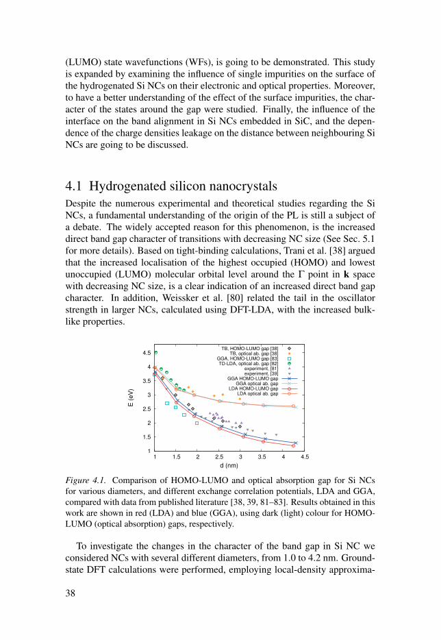
direct band gap character of transitions with decreasing NC size (See Sec. 5.1
for more details). Based on tight-binding calculations, Trani et al. [38] argued
that the increased localisation of the highest occupied (HOMO) and lowest
unoccupied (LUMO) molecular orbital level around the Γ point in k space
with decreasing NC size, is a clear indication of an increased direct band gap
character. In addition, Weissker et al. [80] related the tail in the oscillator
strength in larger NCs, calculated using DFT-LDA, with the increased bulk-
like properties.
1
1.5
2
2.5
3
3.5
4
4.5
1 1.5 2 2.5 3 3.5 4 4.5
E (
eV)
d (nm)
TB, HOMO-LUMO gap [38]TB, optical ab. gap [38]
GGA, HOMO-LUMO gap [83]TD-LDA, optical ab. gap [82]
experiment, [81]experiment, [39]
GGA HOMO-LUMO gapGGA optical ab. gap
LDA HOMO-LUMO gapLDA optical ab. gap
Figure 4.1. Comparison of HOMO-LUMO and optical absorption gap for Si NCs
for various diameters, and different exchange correlation potentials, LDA and GGA,
compared with data from published literature [38, 39, 81–83]. Results obtained in this
work are shown in red (LDA) and blue (GGA), using dark (light) colour for HOMO-
LUMO (optical absorption) gaps, respectively.
To investigate the changes in the character of the band gap in Si NC we
considered NCs with several different diameters, from 1.0 to 4.2 nm. Ground-
state DFT calculations were performed, employing local-density approxima-
38

tion (LDA) and generalised gradient approximation (GGA). Single-ζ polarised
(SZP) and double-ζ (DZ) basis set were used for Si and H, respectively. Each
of the studied structures was relaxed until all forces acting on each atom is
lower than 0.04 eV/Å. For each of the studied structures, the HOMO-LUMO
gaps and the optical absorption gaps were calculated. Shown on Fig. 4.1 are
the calculated HOMO-LUMO gaps and the optical absorption gaps, compared
with experimental band gaps [39, 81], and band gaps from other theoretical
studies [38, 82, 83]. As expected from quantum confinement effect, both
gaps, HOMO-LUMO and optical absorption gap, grow with decreasing NC
size, eventually becoming very close to each other. This apparent merging
of both gaps can be viewed as transition from intrinsic indirect nature of the
band gap, to direct band gap in the smallest NC. It is also interesting to notice
that the HOMO-LUMO gaps are very similar to the optical gaps observed in
experiments. Although the higher-order effects are neglected in the present
DFT results, it is shown that the cancellation of quasi-particle and excitonic
effects [80, 84] contributes to the similarity of the theoretical and experimental
results.
Figure 4.2. HOMO and LUMO WFs of NCs of various sizes. The upper row shows
HOMO WFs on a line passing through NC center parallel to lattice axes, for NCs
of sizes 1.0, 1.9, 3.1, and 4.2 nm, respectively. The lower row show non-degenerate
LUMO WFs of 1.0, 1.5, and 1.9 nm NCs, respectively, then the three perpendicular
cuts of LUMO for the 2.5 nm NC, the triple-degenerated LUMO of the 3.5 nm NC,
and three perpendicular cuts of the bulk LUMO WF.
To facilitate this change in the HOMO-LUMO and optical absorption gap,
some features of the HOMO and LUMO states are most probably changing.
The HOMO state, for example, is triply degenerate for the whole range of NC
size, as in non-relativistic description of bulk Si. However, the LUMO state
changes from non-degenerate in NC smaller than 1.9 nm, to double degenerate
in the 2.5 nm NC, and is triply degenerate for the NCs bigger than 3.1 nm. The
similarity in the HOMO state and the changes in the LUMO state with changes
in the NC size, can be easily observed by inspecting the spatial characteristics
of the WFs. One way to examine this is to plot the HOMO and LUMO WFs
39

on a line passing along the lattice axes, see Fig. 4.2. The HOMO state is triply
degenerate, with a predominantly p character, for which the three WFs have
similar spatial characteristic, displaying an oscillatory behaviour modulated
with Bessel function type [85], decaying at the NC’s edges.
The LUMO state of the NC smaller than 1.9 nm is non-degenerate, and
the LUMO WF has an elliptical s symmetry. The 2.5 nm NC has a double-
degenerate LUMO state, which has a similar spatial distribution of the WFs as
the LUMO WF in the smaller NCs, but with an elliptical distorted s symmetry.
One of the WFs appear compressed along z direction and the other one elon-
gated along z, with the WFs along the x, y and z are almost identical up to a
sign and a scaling factor. On the other hand, the LUMO WFs of the NCs larger
than 3.1 nm have p-type symmetry, with a different spatial characteristic than
the HOMO WFs. Moreover, the LUMO WF of the 3.5 nm NC shows a clear
similarity with the bulk LUMO WF for k point 2πa (0.83,0,0).
Figure 4.3. Fourier transform (FT) of the HOMO (upper row) and LUMO (lower
row) WF of Si NCs of the following sizes: (a) 1.0 nm, (b) 1.9 nm, and (c) 3.1 nm.
(d) Overlap between FT of the HOMO and LUMO WFs for the 4.2 nm NC. The 3D
FT was projected on the x− z plane. For clarity of the graphical representation, the
colour range, blue to red for the HOMO WF and opposite, red to blue, for the LUMO
WF, maps positive values of the real part of FT, within a fixed range for all sizes (in
arbitrary units). The k(x) and k(z) are scaled by a reciprocal vector G of size 2πa .
Further understanding of the changes in the HOMO and LUMO WFs, and
their influence on the k selection rule between the WFs, can be better ex-
plained in Fourier space. In Fig. 4.3 are shown the size-dependence of the
Fourier transform (FT) of the HOMO and LUMO WFs. For the smallest NCs,
the maxima of the Fourier components of the HOMO and LUMO WF display
an increased overlap, indicating no apparent periodicity of the WF in the NC.
With increasing NC size, the maxima of the Fourier components are becom-
ing sharper and isolated, suggesting an increased periodicity, as in periodic
solid. Comparing the position of the Fourier components, it is evident that
with increasing NC size the overlap between the components coming from the
40

HOMO and the LUMO WF is decreasing, eventually the components appear
at different k points. The components of the HOMO WF form arrangement
similar to the one in bulk Si, with the components appearing at odd or even
k points. However, with increasing NC size, the components of the LUMO
WF appear at odd-even combination of k points, shifted towards the origin.
This can be understood as a increasing band-like character of the LUMO WF,
corresponding to the k point 2πa (0.83,0,0). Moreover, the HOMO and LUMO
WF display almost exclusive Fourier components, as in bulk Si, corresponding
to different k points in the Brillouin zone.
4.2 Influence of the surface impurities
Although the Si NCs can emit bright intensity light in narrow spectral range,
their PL can be greatly affected by the surface impurities. It has been shown
that after leaving hydrogenated Si NCs with different sizes in ambient condi-
tions the PL peak does not exhibit blue shift with decreasing NC size, and their
PL intensity is reduced [39, 71, 72]. These observations have been assigned
to the surface oxidation, especially to the localisation of mid-gap states, orig-
inating from the Si=O species on the surface [39]. In addition, the synthesis
of the Si NCs can leave various impurities on the surface of the NCs, which
can further influence the PL properties of the NCs. Therefore, it is impor-
tant to provide understanding of the influence of various surface impurities on
the electronic and optical properties of Si NCs with different sizes, based on
parameter-free DFT calculations.
The main quantity that can be calculated from DFT, and gives direct un-
ambiguous information about the trends in the position of the PL peak, is the
band gap. Thus, obtaining information regarding the changes in the band gap,
in NCs with different impurities, gives an initial insight into the effect of the
surface impurities. Considering that the surface impurities can form different
types of bonds, e.g. single or double-bond, it is also important to examine
the influence of bonding types. Therefore, for the purpose of the study we
considered single-bonded (SB) impurities: –CH3, –F, –Cl, –OH and bridged
oxygen (–O–), and double-bonded impurities: =O and =S. Details of the DFT
calculations are presented in the previous Sec. 4.1. Shown on Fig. 4.4 are the
calculated HOMO-LUMO and optical absorption gaps for the Si NCs with
surface impurities.
Evidently, the SB and DB impurities have rather different influence on the
HOMO-LUMO and optical absorption gap. In the NCs with SB impurity, both
gaps closely follow the gaps in the hydrogenated Si NCs for the respective NC
size. The biggest difference occurs for the smallest NC, 1.0 nm, where the
NCs with SB impurity have slightly lower gaps. The gaps in the NCs with
–O– also closely follow the gaps in the NCs with other SB impurity, but the
–O– impurity induces somewhat larger change in the gaps, which can be seen
41
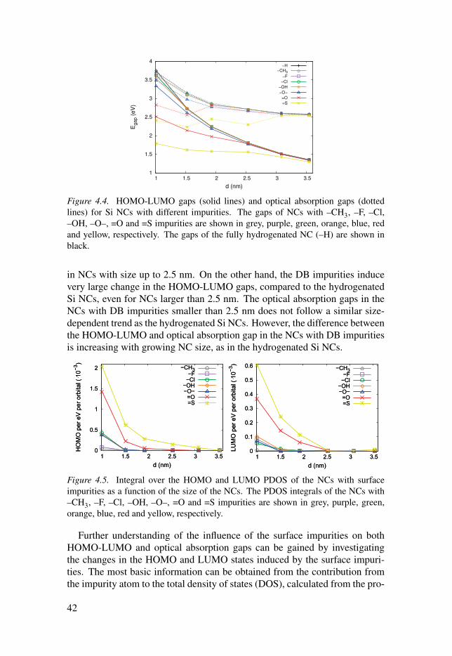
1
1.5
2
2.5
3
3.5
4
1 1.5 2 2.5 3 3.5
Ega
p (e
V)
d (nm)
−H−CH3
−F−Cl
−OH−O−
=O=S
Figure 4.4. HOMO-LUMO gaps (solid lines) and optical absorption gaps (dotted
lines) for Si NCs with different impurities. The gaps of NCs with –CH3, –F, –Cl,
–OH, –O–, =O and =S impurities are shown in grey, purple, green, orange, blue, red
and yellow, respectively. The gaps of the fully hydrogenated NC (–H) are shown in
black.
in NCs with size up to 2.5 nm. On the other hand, the DB impurities induce
very large change in the HOMO-LUMO gaps, compared to the hydrogenated
Si NCs, even for NCs larger than 2.5 nm. The optical absorption gaps in the
NCs with DB impurities smaller than 2.5 nm does not follow a similar size-
dependent trend as the hydrogenated Si NCs. However, the difference between
the HOMO-LUMO and optical absorption gap in the NCs with DB impurities
is increasing with growing NC size, as in the hydrogenated Si NCs.
0
0.5
1
1.5
2
1 1.5 2 2.5 3 3.5
HO
MO
per
eV
per
orb
ital (
103 )
d (nm)
CH3F
ClOHO=O=S
0
0.1
0.2
0.3
0.4
0.5
0.6
1 1.5 2 2.5 3 3.5
LUM
O p
er e
V p
er o
rbita
l (10
3 )
d (nm)
CH3F
ClOHO=O=S
0
0.5
1
1.5
2
1 1.5 2 2.5 3 3.5
HO
MO
per
eV
per
orb
ital (
103 )
d (nm)
CH3F
ClOHO=O=S
0
0.1
0.2
0.3
0.4
0.5
0.6
1 1.5 2 2.5 3 3.5
LUM
O p
er e
V p
er o
rbita
l (10
3 )
d (nm)
CH3F
ClOHO=O=S
Figure 4.5. Integral over the HOMO and LUMO PDOS of the NCs with surface
impurities as a function of the size of the NCs. The PDOS integrals of the NCs with
–CH3, –F, –Cl, –OH, –O–, =O and =S impurities are shown in grey, purple, green,
orange, blue, red and yellow, respectively.
Further understanding of the influence of the surface impurities on both
HOMO-LUMO and optical absorption gaps can be gained by investigating
the changes in the HOMO and LUMO states induced by the surface impuri-
ties. The most basic information can be obtained from the contribution from
the impurity atom to the total density of states (DOS), calculated from the pro-
42

jected DOS (PDOS), see Fig. 4.5. It is evident that the contribution from the
DB impurities to both HOMO and LUMO states is significantly larger than
the contribution from the SB impurities. Moreover, compared to the SB im-
purities, which have significant contribution only for the 1.0 nm NC, the DB
impurities contribute to the HOMO and LUMO states of NCs with larger size,
up to 2.5 nm.
Figure 4.6. Size-dependence of the HOMO and LUMO wavefunctions for Si NCs
with: (a) =O; and (b) –F impurity. The O, F, Si and H atoms are shown in red, green,
tan and white, respectively.
This difference in the contribution can be illustrated in more details by cal-
culating the HOMO and LUMO WFs, see Fig. 4.6. As indicated by the PDOS,
the HOMO and LUMO WFs of the smallest NCs, 1.0 nm, are mainly localised
around the impurity atom, regardless of the type of bonding. With increasing
NC size, the localisation of the WF around the –F impurity is significantly de-
43

ceased, and it is negligible even for the 1.5 nm NC. In the case of the =O im-
purity, there is substantial localisation of the HOMO and LUMO WFs around
the O atom for NCs up to 2.5 nm. It is also interesting to notice that the local-
isation around the =O impurity of the LUMO WF is greater compared to the
localisation of the HOMO WF, especially for larger NCs.
HOMO LUMO(a) Si NCs; =O
HOMO LUMO(b) Si NCs; -F
1.0 nm N
C
k / G0 1 2 3 4-1-2-3-4
01
23
4-1
-2-3
-4k
/ G
k / G0 1 2 3 4-1-2-3-4
01
23
4-1
-2-3
-4k
/ G
0 1 2 3 4-1-2-3-4
01
23
4-1
-2-3
-4
k / G
k / G
k / G0 1 2 3 4-1-2-3-4
01
23
4-1
-2-3
-4k
/ G
1.5 nm N
C
0 1 2 3 4-1-2-3-4
01
23
4-1
-2-3
-4
k / G
k / G
0 1 2 3 4-1-2-3-4
01
23
4-1
-2-3
-4
k / G
k / G
0 1 2 3 4-1-2-3-4
01
23
4-1
-2-3
-4
k / G
k / G
0 1 2 3 4-1-2-3-4
01
23
4-1
-2-3
-4
k / G
k / G
3.1 nm N
C
0 1 2 3 4-1-2-3-4
01
23
4-1
-2-3
-4
k / G
k / G
0 1 2 3 4-1-2-3-4
01
23
4-1
-2-3
-4
k / G
k / G
0 1 2 3 4-1-2-3-4
01
23
4-1
-2-3
-4
k / G
k / G
0 1 2 3 4-1-2-3-4
01
23
4-1
-2-3
-4
k / G
k / G
2.5 nm N
C
0 1 2 3 4-1-2-3-4
01
23
4-1
-2-3
-4
k / G
k / G
0 1 2 3 4-1-2-3-4
01
23
4-1
-2-3
-4
k / G
k / G
0 1 2 3 4-1-2-3-4
01
23
4-1
-2-3
-4
k / G
k / G
0 1 2 3 4-1-2-3-4
01
23
4-1
-2-3
-4
k / G
k / G
3.5 nm N
C
0 1 2 3 4-1-2-3-4
01
23
4-1
-2-3
-4
k / G
k / G
0 1 2 3 4-1-2-3-4
01
23
4-1
-2-3
-4
k / G
k / G
0 1 2 3 4-1-2-3-4
01
23
4-1
-2-3
-4
k / G
k / G
0 1 2 3 4-1-2-3-4
01
23
4-1
-2-3
-4
k / G
k / G
1.9 nm N
C
0 1 2 3 4-1-2-3-4
01
23
4-1
-2-3
-4
k / G
k / G
0 1 2 3 4-1-2-3-4
01
23
4-1
-2-3
-4
k / G
k / G
0 1 2 3 4-1-2-3-4
01
23
4-1
-2-3
-4
k / G
k / G
0 1 2 3 4-1-2-3-4
01
23
4-1
-2-3
-4
k / G
k / G
Figure 4.7. Fourier transform (FT) of the HOMO and LUMO charge density of Si
NCs with: (a) =O; and (b) –F impurity, as a function of the size of the NCs. The FT is
an average of the projections on the x−y, x− z and y− z planes. The red colour maps
the highest values and the blue colour the lowest value of the charge densities within
a fixed range for all sizes (in arbitrary units). The k is scaled by the reciprocal vector
G of size 2πa .
An additional insight and a complementary point of view of the localisation
and the symmetry of the HOMO and LUMO states can be obtained by calcu-
lating the Fourier transform (FT) of the charge densities. Shown on Fig. 4.7 is
the average of the projections on x− y, x− z and y− z planes of the FT of the
44

HOMO and LUMO charge densities. The dependence of the FT of the charge
densities on the size of the NCs naturally follow similar pattern as the WFs in
real space. The FT of both, HOMO and LUMO charge densities of the NC
with =O smaller than 1.9 nm, show an increased delocalisation, indicating an
increased localisation and no apparent periodicity in real space. With increas-
ing NC size, the spots in the FT of the charge densities become more distinct,
suggesting an increased delocalisation in the core of the NC, becoming sim-
ilar to the one in hydrogenated Si NCs (see Fig. 4.3). For the NCs with –F
impurity, the FT of the HOMO and LUMO charge densities of the smallest
NC show increased delocalisation, with the periodicity becoming apparent as
the size of the NC increases.
4.3 Embedded silicon nanocrystalsThe improved properties of silicon upon formation of NCs are also applicable
in photovoltaic devices, as part of the third generation solar cells. However,
to utilise these properties, the Si NCs should be embedded in a host matrix
that serves as a charge carrier. In addition, it is preferable the Si NCs and the
host matrix to form type-II band alignment, where the valence band maximum
(VBM) and conduction band minimum (CBM) of the whole system are in the
different materials. This type of band alignment will provide spatial separation
of the electron and hole, thus reducing the probability of exciton recombina-
tion. Moreover, in this way the charge carrier can be easily transported in the
host matrix, increasing the efficiency of light conversion [75]. It is also prefer-
able the host matrix to have a smaller band gap, which can facilitate faster
transport of the charge carriers [76]. One host matrix which is expected to
posses significantly better properties than the usually used SiO2 and Si3N4, is
amorphous SiC [77–79].
(a) (b) (c)
Figure 4.8. Balls-and-sticks model of: (a) 1.5 nm; (b) 2.0 nm; and (c) 2.5 nm Si NCs,
embedded in 8x8x8 SiC. The Si atoms from the NC are shown in red, and the Si and
C atoms from the matrix are shown in tan and grey, respectively.
To have an insight into the electronic properties of a closely related system,
we focused the study on Si NCs embedded in crystalline SiC. SiC with zinc-
blende structure was used as a host matrix, made of 6x6x6, 7x7x7 and 8x8x8
45

unit cells, and Si NC with 1.5, 2.0 and 2.5 nm in diameter (see Fig. 4.8).
We made four distinct models, termed model A, B, C and D (see Paper III
for more details), where we vary the interface between the Si NC and the
matrix. However, in this section the focus will be on the models A, C and
D. The former being the representatives of a perfect bonding between Si NC
and the matrix, and latter two a case when hydrogenated Si NC or NC with
surface impurities, oxygen in this case, is inserted in the matrix. The electronic
properties of both models were calculated using DFT, with LDA and SZP basis
set for Si, O and C, and DZ for H. In the DOS of model C and D there is a
clearly defined band gap was observed. However, in the same interval around
the Fermi level in model A and B impurity states were noticeable.
Figure 4.9. PDOS of: (a) model C; and (b) model D, and the corresponding projections
of the charge densities on the x−y plane. The PDOS of the core, interface and matrix
region are shown in blue, red and green, respectively.
To have an understanding where do these impurity states come from, and
to have an insight into the band alignment in this complex system, we calcu-
lated the projected DOS (PDOS). Closer inspection of the PDOS of model A
and B revealed that the impurity states are mainly localised at the interface
between the NC and the matrix. Also noticeable from the PDOS was that the
band alignment in models A, B and C is of type-II, with the VBM being in the
NC and the CBM in the host matrix (see Fig. 4.9(a)). Interestingly, there is
46

an interchange in the type-II band alignment in model D, where the VBM is
now in the matrix, and the CBM in the NC (see Fig. 4.9(b)). Having in mind
that model D was made from model C by replacing some H atoms with O, this
switching of the band alignment shows that the band alignment can be mod-
ified depending on the desired properties of the material, just by introducing
particular impurities at the interface of the NC and the matrix.
Model Ay
6x6x
67x
7x7
8x8x
8
Model C
x
2.1 nm1.65 nm
1.2 nm
(a) 1.5 nm NC
1.5
nm N
C2.
0 nm
NC
2.5
nm N
C
yModel A
1.05 nm1.55 nm
2.1 nm
x
Model C(b) 8x8x8 Matrix
(c) | |2 along [100]
0
0.5
1
1.5
2
2.5
15 10 5 0 5 10 150.0010.005
0.02
0.04
0.06
0.08
0.1
||2
r (Å)
x25x25
6x6x67x7x78x8x8
Model A Model C
0
1
2
3
4
5
6
15 10 5 0 5 10 150.010.050.1
0.2
0.3
0.4
0.5
0.6
||2
r (Å)
x10x10
6x6x67x7x78x8x8
0.002
Figure 4.10. Projections of the charge densities on the x− y plane, for two adjacent
cells of models with: (a) 1.5 nm NC in different size matrix; and (b) 8x8x8 matrix
with NCs with different size. The surface-to-surface distances between NCs in neigh-
bouring cells are given on the right side of the each panel. The energy intervals, for
which states the charge densities are calculated, of model A and model C are -0.5 –
-0.3 eV and -0.9 – -0.7 eV, respectively. (c) Average charge densities in a series of
{100} planes along [100] direction, of models A (left part) and C (right part) with 1.5
nm NC, corresponding to the same charge densities shown in (a).
Furthermore, of great interest for photovoltaic applications is also the pos-
sible leakage of states between the neighbouring NCs. Thus, we focused on
the leakage of the charge densities of the states that are mostly localised in
the core of the NC. Shown in Fig. 4.10 are the x− y projection of the charge
densities of two adjacent cells of model A and C, as a function of the distance
between the Si NCs. Two possible instances are considered: (a) changing the
NC distance by keeping the NC size fixed while changing the matrix size, and
(b) changing the size of the NCs, in a host matrix with fixed size. With increas-
47

ing matrix size, the spatial distribution of the charge densities of a particular
model is rather unchanged. However, the leakage of the charge densities in the
neighbouring cells is increasing with narrowing distance between the NCs, be-
ing the largest when the NC–NC distance is the shortest, ∼1.2 nm. This can be
clearly seen from Fig. 4.10(c), where the charge density at the border of two
cells is ∼0.8 % from the maximum. The leakage is significantly smaller when
the NC–NC distance ∼1.65 nm, and is almost absent for the largest NC–NC
distance, ∼2.1 nm, being smaller than ∼ 0.05 %. Similarly, when the size of
the NC is increasing, in host matrix with same size, the leakage of the charge
densities is growing with growing NC size, i.e. decreasing NC distance. The
leakage of the states is largest for the biggest NC, where significant overlap
between the charge densities of the neighbouring cells is observed, with the
charge density at the border of two cells being more than 2 % of the max-
imum. Moreover, in the systems with similar NC–NC distance, ∼1.65 and
∼1.55 nm (8x8x8 matrix with 2.0 nm NC and 7x7x7 matrix with 1.5 nm NC),
the leakage of the states is very similar, indicating that the size of the NC does
not affect the leakage of the charge densities.
48

5. Semiconductor nanocrystals – significanceof the interface and the capping of thesurface
The semiconductor nanocrystals (NCs) are mediators between the bulk ma-
terials and isolated molecules, having the usefulness of the crystalline mate-
rials and displaying quantised electronic states as in isolated molecules. The
quantisation of the electronic states arises from the spatial confinement of the
bulk delocalised states, which also influences the band gap. With increasing
confinement, i.e. reducing nanocrystal size, the band gap exhibits blue shift,
allowing for the electronic and optical properties to be tailored according to
the specific needs, which makes the semiconductor NCs very desirable ma-
terials in various applications. Another important benefit from confining the
dimensions is the increase in the photoluminescence (PL) quantum efficiency
(QE) of the semiconductor, which even further increases the usability of the
semiconductor NCs. The QE can be defined as the ratio between the amount
of photons emitted, Ne, and the amount of photons absorbed Na, i.e.:
QE =Ne
Na, (5.1)
In a perfect nanocrystal, where every recombination of an excited electron
with hole is coupled with photon emission, the QE would always be 100 %.
However, the synthesised NCs might exhibit many defects and dislocations,
and together with the increased surface area can facilitate other recombination
processes that can decrease the QE. For example, in non-radiative and Auger
processes the absorbed energy is not emitted, but it is merely lost in a different
form. These processes can also reduce the PL intensity, broaden the PL peak,
and facilitate random switching between PL on and off states, i.e. blinking.
Furthermore, the improved methods of producing semiconductor NCs with
uniform size and very high quality, together with the NCs’ increased PL effi-
ciency in narrow spectral range, has turned the attention to these NCs as one
of the essential materials in many aspects of science and technology. Their
applicability ranges from devices where high-intensity light is required, e.g.
LEDs [86–90] and lasers [91], to using their absorption properties in pho-
tovoltaic materials [75, 92, 93], as well as biological sensors and biological
labelling [94, 95]. The usefulness of the semiconductor NCs comes mainly
from the easiness of influencing the band gap, allowing the PL to be shifted
49

to particular spectral range just by manipulating the NCs size. This versatil-
ity has made the semiconductor NCs especially attractive materials in devices
where tunability of the PL is necessary.
As in the case of the Si NCs, the PL in any other semiconductor NC can be
significantly influenced by the surface impurities. To suppress the addition of
impurities, the surface of the NCs is capped. In the case of compound semi-
conductor NCs, II-VI semiconductor NCs for example, there are differently
charged anionic and cationic sites on the surface. The passivation of their sur-
face with organic molecules has been proven difficult, because of the difficulty
to simultaneously passivate both cationic and anionic sites. Therefore, to sup-
press the dangling bonds that might appear and to fully passivate the surface,
the II-VI semiconductor NCs are overgrown with another semiconductor, act-
ing as a capping shell, making core-shell NCs. Of special interest are the NCs
with type-I band alignment, where both the electron and hole are confined in
the core of the NC, which improves the PL properties of the core material and
further increase their PL intensity. Core-shell NCs which are shown to exhibit
these properties, increasing their usability in wide variety of applications, are
the CdSe/CdS [96–102] and CdS/ZnS [103–105].
The properties of the core-shell NCs can be further adapted to the spe-
cific needs by engineering the interface between the core and the shell, or by
changing the core type. It has been shown that by introducing alloyed in-
terface between CdSe core and CdS shell, the Auger recombination can be
suppressed [99, 101], compared to the same size NCs with sharp interface.
Also, in CdSe/CdS core-shell NCs, introducing graded core can increase the
quantum efficiency of the NCs [97]. The aim of our research was to under-
stand how the different structural models influence the properties of CdSe/CdS
and CdS/ZnS core-shell NCs, and compare the properties of these two differ-
ent types of core-shell NCs. We also focus on the changes in the properties
of these core-shell NCs with changes in the size of the NC and the core/shell
ratio. The results are presented in detail in Papers IV and V.
On the other hand, in single element semiconductor NCs, for example Si
NCs, the situation is different. Having only one type of atom, makes the sur-
face of the NCs uniformly charged, and thus easier to be passivated. Capping
the surface of Si NCs with organic ligands suppresses the oxidation of the
surface, and increases the radiative transition rates [106–110], making the ra-
diative rates of these NCs comparable to the ones in direct semiconductor NCs.
However, the energy and the intensity of the emitted light can be influenced
by the organic ligand used to passivate the surface [107]. The increased PL of
the Si NCs upon capping the surface with organic ligands, and comparison be-
tween two different types of ligands, was the main topic of the study presented
in Paper VI.
Before giving further details regarding the results from the different stud-
ies of semiconductor NCs, a short descriptions of the various recombination
processes that can occur in semiconductor nanocrystals are presented. Af-
50

terwards, the influence of the different structural models on the properties of
CdSe/CdS and CdS/ZnS core-shell nanocrystals are going to be presented,
as well as direct comparison between these two different types of core-shell
nanocrystals. In the subsequent section, the effect of the surface capping on
the properties of Si nanocrystals is going to be discussed.
5.1 Recombination processes in semiconductornanocrystals
5.1.1 Radiative recombination
Any recombination process is preceded by an absorption of energy, during
which an electron is excited from the valence band to the conduction band,
creating an electron hole (e-h) pair. Once the e-h pair is formed, both electron
and hole reach their respective conduction and valence band edges in matter
of ps, due to the coupling with lattice vibrations. The bound state in which
the electron and the hole are attracted by electrostatic Coulomb force, form-
ing a neutral quasi-particle, is called exciton. The process of electron and
hole annihilation (recombination) accompanied by a generation of photon is
termed radiative recombination. The emitted photon has energy equal to the
energy difference between the eigenstates of the electron and the hole. This is
schematically represented in Fig. 5.1.
Ev
Ec
Eg=Eg
E
Figure 5.1. Schematic representation of radiative recombination process. The electron
and hole are shown in blue and red balls, respectively.
In direct band gap semiconductors, such as CdSe, CdS and ZnS discussed in
this Chapter, both conduction band minimum (CBM) and valence band max-
imum (VBM) are at the Γ point (k = 0). Hence, the transitions between the
CBM and VBM are happening at the same k point, which gives the term di-
rect transitions. In a radiative recombination event, the energy of the emitted
photon equals the band gap energy, hω = Eg. On the other hand, the interband
51
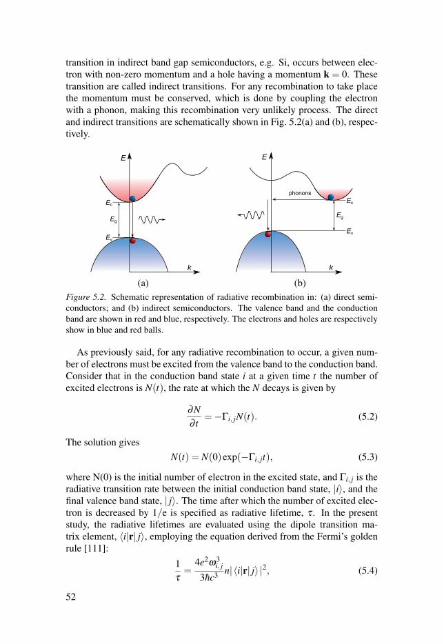
transition in indirect band gap semiconductors, e.g. Si, occurs between elec-
tron with non-zero momentum and a hole having a momentum k = 0. These
transition are called indirect transitions. For any recombination to take place
the momentum must be conserved, which is done by coupling the electron
with a phonon, making this recombination very unlikely process. The direct
and indirect transitions are schematically shown in Fig. 5.2(a) and (b), respec-
tively.
E
k
Ev
Ec
Eg
E
k
phonons
Ev
Ec
Eg
(a) (b)
Figure 5.2. Schematic representation of radiative recombination in: (a) direct semi-
conductors; and (b) indirect semiconductors. The valence band and the conduction
band are shown in red and blue, respectively. The electrons and holes are respectively
show in blue and red balls.
As previously said, for any radiative recombination to occur, a given num-
ber of electrons must be excited from the valence band to the conduction band.
Consider that in the conduction band state i at a given time t the number of
excited electrons is N(t), the rate at which the N decays is given by
∂N∂ t
=−Γi, jN(t). (5.2)
The solution gives
N(t) = N(0)exp(−Γi, jt), (5.3)
where N(0) is the initial number of electron in the excited state, and Γi, j is the
radiative transition rate between the initial conduction band state, |i〉, and the
final valence band state, | j〉. The time after which the number of excited elec-
tron is decreased by 1/e is specified as radiative lifetime, τ . In the present
study, the radiative lifetimes are evaluated using the dipole transition ma-
trix element, 〈i|r| j〉, employing the equation derived from the Fermi’s golden
rule [111]:
1
τ=
4e2ω3i, j
3hc3n| 〈i|r| j〉 |2, (5.4)
52

where ωi, j is the emission frequency between the initial and final state, h is the
reduced Planck constant, and c is the speed of light in vacuum. The refrac-
tive index of the system, n, is evaluated from the calculated dielectric tensor.
As mentioned previously, the attraction between the electron and hole in the
excitonic state is dependent on the Coulomb force. Therefore, valuable in-
formation concerning the stability of the exciton can be obtained from the
electron-hole (e-h) Coulomb interaction energy (Eb). The e-h Eb was calcu-
lated employing the equation proposed by Wang et al. [112]:
Eb =∫ ∫ |ψe(r1)|2|ψh(r2)|2
ε(r1 − r2)|r1 − r2|dr1dr2, (5.5)
where ψe and ψh are the electron and hole wavefunctions, respectively, and
ε(r1 − r2) is the screening dielectric constant.
5.1.2 Non-radiative recombination
Eg
E
Et or
Ev
Ec
Heat(phonons)
Figure 5.3. Schematic representation of non-radiative (trap assisted) recombination
processes. The electrons and holes are shown in blue and red balls, respectively.
As the name suggests, during a non-radiative recombination, also known
as trap assisted recombination, no photons are emitted, while the energy is
dissipated in the lattice, in form of phonons. The recombination of the electron
and hole occurs through localised state (trap state) in the band gap, during
which the electron and hole can annihilate at the trap state, or the electron
can relax to the valence band in two-step recombination. These two processes
are schematically shown in Fig. 5.3. In very few cases when trap states are
involved in the annihilation of the electron-hole pair, photon with low energy
might be emitted, which significantly broadens the PL peak. The allowed
energy levels (Et) in otherwise forbidden gap can arise due to impurities and
defects in the semiconductor. Especially the surface, which can be seen as
a serious defect, can introduce great number of allowed states in the band
53
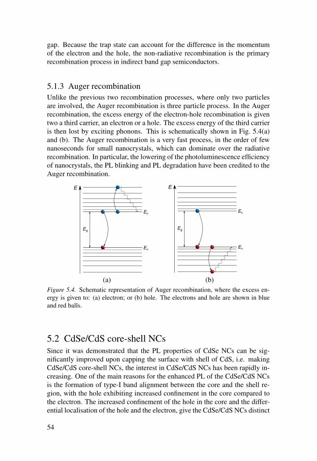
gap. Because the trap state can account for the difference in the momentum
of the electron and the hole, the non-radiative recombination is the primary
recombination process in indirect band gap semiconductors.
5.1.3 Auger recombination
Unlike the previous two recombination processes, where only two particles
are involved, the Auger recombination is three particle process. In the Auger
recombination, the excess energy of the electron-hole recombination is given
two a third carrier, an electron or a hole. The excess energy of the third carrier
is then lost by exciting phonons. This is schematically shown in Fig. 5.4(a)
and (b). The Auger recombination is a very fast process, in the order of few
nanoseconds for small nanocrystals, which can dominate over the radiative
recombination. In particular, the lowering of the photoluminescence efficiency
of nanocrystals, the PL blinking and PL degradation have been credited to the
Auger recombination.
Ev
Ec
Eg
E
Ev
Ec
Eg
E
(a) (b)
Figure 5.4. Schematic representation of Auger recombination, where the excess en-
ergy is given to: (a) electron; or (b) hole. The electrons and hole are shown in blue
and red balls.
5.2 CdSe/CdS core-shell NCsSince it was demonstrated that the PL properties of CdSe NCs can be sig-
nificantly improved upon capping the surface with shell of CdS, i.e. making
CdSe/CdS core-shell NCs, the interest in CdSe/CdS NCs has been rapidly in-
creasing. One of the main reasons for the enhanced PL of the CdSe/CdS NCs
is the formation of type-I band alignment between the core and the shell re-
gion, with the hole exhibiting increased confinement in the core compared to
the electron. The increased confinement of the hole in the core and the differ-
ential localisation of the hole and the electron, give the CdSe/CdS NCs distinct
54
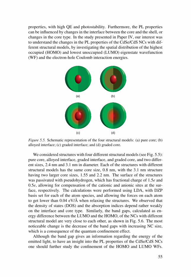
properties, with high QE and photostability. Furthermore, the PL properties
can be influenced by changes in the interface between the core and the shell, or
changes in the core type. In the study presented in Paper IV, our interest was
to understand the changes in the PL properties of the CdSe/CdS NCs with dif-
ferent structural models, by investigating the spatial distribution of the highest
occupied (HOMO) and lowest unoccupied (LUMO) eigenstate wavefunction
(WF) and the electron-hole Coulomb interaction energies.
(a) (b)
(c) (d)
Figure 5.5. Schematic representation of the four structural models: (a) pure core; (b)
alloyed interface; (c) graded interface; and (d) graded core.
We considered structures with four different structural models (see Fig. 5.5):
pure core, alloyed interface, graded interface, and graded core, and two differ-
ent sizes, 2.4 nm and 3.1 nm in diameter. Each of the structures with different
structural models has the same core size, 0.8 nm, with the 3.1 nm structure
having two larger core sizes, 1.55 and 2.2 nm. The surface of the structures
was passivated with pseudohydrogen, which has fractional charge of 1.5e and
0.5e, allowing for compensation of the cationic and anionic sites at the sur-
face, respectively. The calculations were performed using LDA, with DZP
basis set for each of the atom species, and allowing the forces on each atom
to get lower than 0.04 eV/Å when relaxing the structures. We observed that
the density of states (DOS) and the absorption indices depend rather weakly
on the interface and core type. Similarly, the band gaps, calculated as en-
ergy difference between the LUMO and the HOMO, of the NCs with different
structural model are very close to each other, as shown in Fig. 5.6. The most
noticeable change is the decrease of the band gaps with increasing NC size,
which is a consequence of the quantum confinement effect.
Although the band gap gives an information regarding the energy of the
emitted light, to have an insight into the PL properties of the CdSe/CdS NCs
one should further study the confinement of the HOMO and LUMO WFs.
55

1.75
1.85
1.95
2.05
2.4 2.5 2.6 2.7 2.8 2.9 3 3.1
Ega
p (e
V)
d (nm)
Egap(1.1 nm pure CdSe NC) = 3.6 eV
0.8 nm pure core1.55 nm pure core2.2 nm pure core
graded corealloyed interfacegraded interface
Figure 5.6. Band gaps of CdSe/CdS core-shell NCs with different size, made using
different structural models and core sizes.
The increased localisation of the HOMO and LUMO WFs in the core of the
CdSe/CdS NCs, decreases the probability of non-radiative recombinations and
photo-oxidation of the hole at the surface, increasing the QE. Hence, we cal-
culated the confinement of the HOMO and LUMO WF, ψ(r), as:
I|WF|2 =∫ r0
0|ψ(r)|2dr (5.6)
using four different values for the integration radius, r0, 2.6 Å, 4.9 Å, 8.7 Å,
and 12.1 Å. The resulting confinement of both HOMO and LUMO WFs as
a function of r0, are shown in Fig. 5.7. Evidently, the confinement of the
HOMO WF in the core of the NCs is significantly larger than the confinement
of the LUMO WF, and exhibits significant dependence on the core size and the
model type. With increasing core/shell ratio, the confinement of the HOMO
WF decreases, suggesting that the NCs with smaller core would have higher
QE. Moreover, in the NCs with different structural model and same core size,
0.8 nm, the confinement of the HOMO WF is rather similar, except in the NC
with pure core, which shows slightly higher confinement. From this difference
in the confinement, it is expected the the NCs with different structural model
will have similar QE, with the NC with pure core having somewhat higher
QE. It is also noticeable that the confinement of the HOMO WF increases
with decreasing NC size, indicating that lowering the NC size would increase
the QE.
In addition, the spatial distribution of the HOMO WF can influence the
Auger recombination (AR) rates, causing the AR rates to decrease with in-
crease spread of the HOMO WF [113], which in turn will increase the QE of
the NCs. Therefore, the decreased confinement of the HOMO WF in the NCs
with alloyed and graded interface, is likely to induce lowering of the AR rates,
compared to the NC with 0.8 nm pure core. In the NCs with different size of
the pure core, it is expected that the AR rates to decrease with growing core
56

(a) 3.1 nm NCs
HOMO
(d) 2.4 nm NCsLUMO
(c) 2.4 nm NCs
0
0.1
0.2
0.3
0.4
0.5
0.6
0.7
0.8
0.9
2 3 4 5 6 7 8 9 10 11 12 13
I |HO
MO
|2(c
ore
)
r0 (Å)
0.8 nm pure core1.55 nm pure core
2.2 nm pure coregraded core
alloyed interfacegraded interface
HOMO
0
0.1
0.2
0.3
0.4
0.5
0.6
0.7
0.8
2 3 4 5 6 7 8 9 10 11 12 13
I |LU
MO
|2(c
ore
)
r0 (Å)
0.8 nm pure core1.55 nm pure core
2.2 nm pure coregraded core
alloyed interfacegraded interface
(b) 3.1 nm NCsLUMO
0
0.1
0.2
0.3
0.4
0.5
0.6
0.7
0.8
0.9
2 3 4 5 6 7 8 9
I |HO
MO
|2(c
ore
)
r0 (Å)
0.8 nm pure corealloyed interface
0
0.1
0.2
0.3
0.4
0.5
0.6
0.7
0.8
2 3 4 5 6 7 8 9I |L
UM
O|2
(co
re)
r0 (Å)
0.8 nm pure corealloyed interface
Figure 5.7. Comparison between the confinement of the HOMO and LUMO WFs
respectively of: (a) and (b) 2.4 nm NCs; and (c) and (d) 3.1 nm NCs, with different
structural models, as a function of the core integration radius, r0.
size, following the decreasing confinement of the HOMO WF. Another quan-
tity that can give further information regarding the AR, is the electron-hole
(e-h) Coulomb interaction energy (Eb). To evaluate the e-h Eb, Eq. 5.5 was
used, and the calculated e-h Eb are shown in Fig. 5.8.
0.22
0.23
0.24
0.25
0.26
0.27
0.28
0.29
0.3
0.31
0.32
2.4 2.5 2.6 2.7 2.8 2.9 3 3.1
Eb
(eV
)
d (nm)
0.8 nm pure core1.55 nm pure core2.2 nm pure core
graded corealloyed interfacegraded interface
Figure 5.8. Electron-hole Coulomb interaction energies, Eb, of CdSe/CdS core-shell
NCs with different size, made using different structural models and core size.
It is evident that the e-h Eb are reduced with increasing core size, in the
NC with same size. Considering that the AR rates decrease with increased e-h
Eb [113], and the lower AR rates contribute to increase QE, the lowering of the
e-h Eb with increasing core size indicates that the NCs with largest core would
have higher QE. In the NCs with different structural models, the e-h Eb are
57

very similar, with the NC with 0.8 nm pure core exhibiting higher e-h Eb. This
suggests that introducing alloyed or graded interface between the core and the
shell lowers the e-h Eb, and hence can decrease the AR rates, increasing the
QE of the CdSe/CdS NCs.
5.3 CdS/ZnS core-shell NCs
Another interesting example where making core-shell NCs can greatly im-
prove the properties, are the CdS/ZnS core-shell NCs. The overcoating of the
CdS NCs with ZnS shell suppresses the deep-trap white luminescence other-
wise exhibited by the bare CdS NCs, suppressing the non-radiative transitions.
The CdS/ZnS NCs produced in this way are very suitable for light-emitting
devices, especially because of their high intensity blue light. However, un-
like the CdSe/CdS NCs which have been extensively studied experimentally
and theoretically, until now for the CdS/ZnS NCs there have not been any re-
ported studies of the dependence of the PL properties on the structural model
nor theoretical studies of the size-dependence of the PL properties. There-
fore, we focused the study on the understanding how the size of the NCs and
the different structural models can influence the PL properties. Similarly to
the CdSe/CdS NCs, we investigated the band gaps, the spatial distribution of
HOMO and LUMO WFs and the electron-hole Coulomb interaction energies.
1.5
2
2.5
3
Bulk 3.4 2.9 2.3 1.8
Ega
p (e
V)
d (nm)
bulk CdSbulk ZnS
2.2 nm core1.8 nm core1.4 nm core1.0 nm core0.7 nm core
NCs with same shell size 2.1
2.2
2.3
2.4
2.5
2.6
2.7
2.8
2.9
3
3.1
2.3 2.4 2.5 2.6 2.7 2.8 2.9
Ega
p (e
V)
d (nm)
Egap(1.0 nm CdS NC) = 3.8 eV
0.7 nm pure core1.4 nm pure core1.8 nm pure core
graded coregraded interfacealloyed interface
graded shell
(a) (b)
Figure 5.9. Band gaps of CdS/ZnS core-shell NCs as a function of: (a) as a function
of the NC size; and (b) different structural model. The dashed line in (a) connects the
gaps of NCs with same shell size.
To study the size dependence of the PL properties, NCs with four different
sizes were made, and we inserted cores with five different size, depending on
the size of the NCs. Moreover, from the 2.3 and 2.9 nm NCs we constructed
NCs with the same structural models as in the CdSe/CdS NCs. The surface
of the each of the studied NCs is completely passivated with pseudohydrogen.
The calculations were performed in the same manner as described in the previ-
ous section, Sec. 5.2. When comparing the DOS and the absorption indices of
58

the NCs with different size, and same core size, rather small differences were
observed. Also, we observed rather weak dependence of the DOS and the
absorption indices on the core/shell ratio and the different structural model.
However, the changes in the band gap with changes in the NC size and
core/shell ratio are significantly larger (see Fig. 5.9(a)), which comes mainly
from the large difference in the band gap of the bulk CdS and ZnS. Following
the quantum confinement effect, the band gaps are increasing with decreasing
NC size, as well as with decreasing core size. Moreover, the dependence on
the core size is less pronounced than the dependence on the shell size, which
can be attributed to the notable increase in the shell material, ZnS, when the
shell size is growing, compared to the increase in the core material, CdS. In the
NCs with different structural models, the band gaps are very similar, except
when the NCs have very small or very large core, where considerable increase
or reduction of the band gap are respectively evident (see Fig. 5.9(b)).
(c) LUMO; same core0.05
0.1
0.15
0.2
0.25
0.3
0.35
0.4
1.8 2 2.2 2.4 2.6 2.8 3 3.2 3.4
I |LU
MO
|2 (co
re)
dNC (nm)
1 ML ZnS2 ML ZnS3 ML ZnS
(d) LUMO; same shell0.05
0.1
0.15
0.2
0.25
0.3
0.35
0.4
1.8 2 2.2 2.4 2.6 2.8 3 3.2 3.4
I |LU
MO
|2 (co
re)
dNC (nm)
graded interface2.2 nm core1.8 nm core1.4 nm core1.0 nm core0.7 nm core
0.1
0.15
0.2
0.25
0.3
0.35
0.4
0.45
0.5
1.8 2 2.2 2.4 2.6 2.8 3 3.2 3.4
I |HO
MO
|2 (co
re)
dNC (nm)
1 ML ZnS2 ML ZnS3 ML ZnS
(b) HOMO; same shell(a) HOMO; same core 0.1
0.15
0.2
0.25
0.3
0.35
0.4
0.45
0.5
1.8 2 2.2 2.4 2.6 2.8 3 3.2 3.4
I |HO
MO
|2 (co
re)
dNC (nm)
graded interface2.2 nm core1.8 nm core1.4 nm core1.0 nm core0.7 nm core
Figure 5.10. Comparison between the confinement of the HOMO and LUMO WFs
in NCs with: (a) and (c) same core size, respectively; (b) and (d) same shell size,
respectively; as a function of the NCs size. The confinement in calculated using the
same core integration radius, r0 = 4.7 Å (corresponding to the smallest pure core).
As in the CdSe/CdS core-shell NCs, in the CdS/ZnS NCs both the electron
and the hole are confined in the core of the NCs. This type of band alignment
is exhibited throughout the whole series of studied NCs. Having both electron
and hole confined in the core of the NC, lowers the probability of non-radiative
transitions at surface traps, increasing the QE of the NCs. Therefore, to under-
stand how much the HOMO and LUMO WFs are localised in the core of the
NC, we calculated confinement of the WFs using Eq. 5.6, using r0 = 4.7 Å,
and plotted them as a function of the size of the NCs (see Fig. 5.10). Clearly,
the confinement of both the HOMO and LUMO WFs decreases with increas-
59
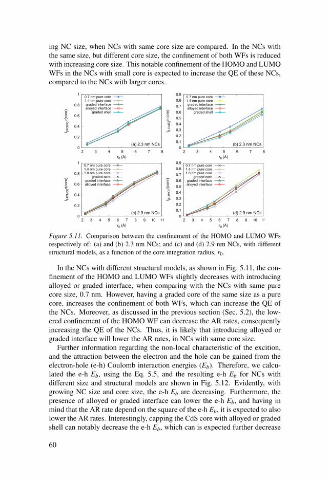
ing NC size, when NCs with same core size are compared. In the NCs with
the same size, but different core size, the confinement of both WFs is reduced
with increasing core size. This notable confinement of the HOMO and LUMO
WFs in the NCs with small core is expected to increase the QE of these NCs,
compared to the NCs with larger cores.
00.10.20.30.40.50.60.70.80.9
2 3 4 5 6 7 8
I |LU
MO
|2 (co
re)
r0 (Å)
0.7 nm pure core1.4 nm pure coregraded interfacealloyed interface
graded shell
0
0.2
0.4
0.6
0.8
1
2 3 4 5 6 7 8
I |HO
MO
|2 (co
re)
r0 (Å)
0.7 nm pure core1.4 nm pure coregraded interfacealloyed interface
graded shell
(c) 2.9 nm NCs
(a) 2.3 nm NCs (b) 2.3 nm NCs
(d) 2.9 nm NCs0
0.2
0.4
0.6
0.8
1
2 3 4 5 6 7 8 9 10 11
I |HO
MO
|2 (co
re)
r0 (Å)
0.7 nm pure core1.4 nm pure core1.8 nm pure core
graded coregraded interfacealloyed interface
00.10.20.30.40.50.60.70.80.9
2 3 4 5 6 7 8 9 10 11
I |LU
MO
|2 (co
re)
r0 (Å)
0.7 nm pure core1.4 nm pure core1.8 nm pure core
graded coregraded interfacealloyed interface
Figure 5.11. Comparison between the confinement of the HOMO and LUMO WFs
respectively of: (a) and (b) 2.3 nm NCs; and (c) and (d) 2.9 nm NCs, with different
structural models, as a function of the core integration radius, r0.
In the NCs with different structural models, as shown in Fig. 5.11, the con-
finement of the HOMO and LUMO WFs slightly decreases with introducing
alloyed or graded interface, when comparing with the NCs with same pure
core size, 0.7 nm. However, having a graded core of the same size as a pure
core, increases the confinement of both WFs, which can increase the QE of
the NCs. Moreover, as discussed in the previous section (Sec. 5.2), the low-
ered confinement of the HOMO WF can decrease the AR rates, consequently
increasing the QE of the NCs. Thus, it is likely that introducing alloyed or
graded interface will lower the AR rates, in NCs with same core size.
Further information regarding the non-local characteristic of the excition,
and the attraction between the electron and the hole can be gained from the
electron-hole (e-h) Coulomb interaction energies (Eb). Therefore, we calcu-
lated the e-h Eb, using the Eq. 5.5, and the resulting e-h Eb for NCs with
different size and structural models are shown in Fig. 5.12. Evidently, with
growing NC size and core size, the e-h Eb are decreasing. Furthermore, the
presence of alloyed or graded interface can lower the e-h Eb, and having in
mind that the AR rate depend on the square of the e-h Eb, it is expected to also
lower the AR rates. Interestingly, capping the CdS core with alloyed or graded
shell can notably decrease the e-h Eb, which can is expected further decrease
60

0.2
0.25
0.3
0.35
0.4
0.45
0.5
1.8 2 2.2 2.4 2.6 2.8 3 3.2 3.4
Eb(
eV)
d (nm)
2.2 nm core1.8 nm core1.4 nm core1.0 nm core0.7 nm core
graded interface
0.29
0.3
0.31
0.32
0.33
0.34
0.35
0.36
0.37
0.38
0.39
0.4
2.3 2.4 2.5 2.6 2.7 2.8 2.9
Eb(
eV)
d (nm)
0.7 nm pure core1.4 nm pure core1.8 nm pure core
graded coregraded interfacealloyed interface
graded shell
(a) (b)
Figure 5.12. Electron-hole Coulomb interaction energies (Eb) of CdS/ZnS core-shell
NCs as a function of: (a) as a function of the NC size; and (b) different structural
model.
the AR rate and increase the QE, but the defects that appear on the surface can
significantly reduce the QE by facilitating non-radiative transitions, which has
been shown experimentally [101].
5.4 Comparison between CdSe/CdS and CdS/ZnScore-shell NCs
Although the CdSe/CdS and CdS/ZnS core-shell NCs are composed of very
similar elements, they exhibit somewhat different PL properties. One of the
reasons might be in the constituent elements in the core and the shell, specifi-
cally the CdSe/CdS NCs have common cation, and the CdS/ZnS common an-
ion. Therefore, it is very interesting to investigate the changes in the properties
of the NCs, when going from CdSe/CdS to CdS/ZnS NCs. In this section, a di-
rect comparison between the band gaps, localisation of the HOMO and LUMO
WFs, radiative lifetimes and the electron-hole Coulomb interaction energies in
CdSe/CdS and CdS/ZnS NCs is going to be presented. Details regarding the
considered NC sizes, structural models, and the calculations are given in the
previous two sections (Sec. 5.2 and Sec. 5.3). Comparison between the prop-
erties of the CdSe/CdS and CdS/ZnS 2.4 nm and 2.3 nm NCs, respectively,
both of which have 317 atoms, and the 3.1 and 2.9 nm NCs, respectively, with
633 atoms, is going to be given. For the larger NCs, 633 atoms, we are also
going to compare the properties of the CdSe/CdS and CdS/ZnS NCs with three
different core sizes1: (i) 0.8 and 0.7 nm (29 atoms), (ii) 1.55 and 1.4 nm (123
atoms), and (iii) 2.2 and 1.8 nm (287 atoms), respectively.
1The CdSe and CdS cores with similar size, have the same number of cations and anions. The
difference in their size comes from the difference in the lattice parameter of the core materials,
CdSe and CdS.
61

1.8
2
2.2
2.4
2.6
2.8
3
CdS/ZnS CdSe/CdS CdS/ZnS CdSe/CdS
Eg
(eV
)
317 atoms NCs 633 atoms NCs
29 atoms pure core123 atoms pure core287 atoms pure core
graded corealloyed interfacegraded interface
Figure 5.13. Comparison between the band gaps of CdS/ZnS and CdSe/CdS core-
shell NCs, with two different sizes of NCs, 317 and 633 atoms (see the text for more
details), and different structural models.
The influence of the different structural models on the DOS and the absorp-
tion indices in both types of NCs is rather weak, as discussed before. Similar
behaviour can be also observed for the band gaps of both types of NCs with
different structural models (see Fig. 5.13). However, there is significant differ-
ence between the change in the band gaps with changes of the structural model
of the CdSe/CdS and of the CdS/ZnS NCs. The band gaps of the CdS/ZnS
NCs are influenced more by the different structural models, compared to the
CdSe/CdS NCs. This difference in the band gaps of both types of the NCs is
a consequence of the larger difference in the band gaps of bulk CdS and ZnS,
compared to the difference in CdSe and CdS bulk band gaps.
0.2
0.25
0.3
0.35
0.4
CdS/ZnS CdSe/CdS CdS/ZnS CdSe/CdS
I |HO
MO
|2 (co
re)
317 atoms NCs 633 atoms NCs
29 atoms pure core123 atoms pure core287 atoms pure core
graded corealloyed interfacegraded interface
0.05
0.1
0.15
0.2
0.25
CdS/ZnS CdSe/CdS CdS/ZnS CdSe/CdS
I |LU
MO
|2 (co
re)
317 atoms NCs 633 atoms NCs
29 atoms pure core123 atoms pure core287 atoms pure core
graded corealloyed interfacegraded interface
(a) (b)
Figure 5.14. Comparison between the confinement of the: (a) HOMO WF; and (b)
LUMO WF, in CdS/ZnS and CdSe/CdS core-shell NCs, with two different sizes of
NCs, 317 and 633 atoms (see the text for more details), and different structural models.
The confinement is calculated within the smallest pure core.
As discussed before, the QE of the core-shell NCs is influenced by the spa-
tial distribution of the HOMO and LUMO WFs. Thus, acquiring information
62
regarding the spread of both WFs in the CdSe/CdS and CdS/ZnS NCs, can
give valuable information for the understanding of the different PL properties
of the two types of core-shell NCs. Shown in Fig. 5.14 are the calculated con-
finement of the HOMO and LUMO WFs of the CdSe/CdS and CdS/ZnS NCs,
using Eq. 5.6, with integration radius, r0, that corresponds to the distance from
the center to the farthest most atom in the smallest core. It is noticeable that
in both types of core-shell NCs the confinement of the HOMO WF is fairly
similar, and the dependence on the different structural models is also rather
comparable. Based on this observation, and keeping in mind the correlation
between the confinement of the HOMO WF and the AR rates, it is expected
the CdSe/CdS and CdS/ZnS NCs to have similar QE. On the other hand, the
extent of the confinement of the LUMO WF is very different in the CdSe/CdS
and CdS/ZnS NCs. It is evident that the confinement in the CdSe/CdS NCs
is significantly smaller than the confinement in the CdS/ZnS NCs, indicating
increased spread of the LUMO WF in the CdSe/CdS NCs.
2.31 eV
0.67 eV
0.13 eV
3.11
eV
Ener
gy
CdS ZnS
core shell
r=0 r
(d) CdS/ZnS
1.78 eV
0.29 eV
0.61 eV
2.68
eV
Ener
gy
CdSe CdS
core shell
r=0 r
(c) CdSe/CdS
(a) HOMO
(b) LUMO
0
0.2
0.4
0.6
0.8
1
1.2
1.4
1.6
0 2 4 6 8 10 12 14 16 18
|LU
MO
|2
r (Å)
CdS/ZnS NCCdSe/CdS NC
0
0.5
1
1.5
2
0 2 4 6 8 10 12 14 16 18
|HO
MO
|2
r (Å)
CdS/ZnS NCCdSe/CdS NC
Figure 5.15. (a) Radial distribution of the density of: (a) HOMO WF (b) LUMO WF.
The red and blue arrows represent the distance from the NC center to the farthest atom
of the core in CdSe/CdS and CdS/ZnS NCs, respectively. Schematic representation
of the band alignment in: (c) CdSe/CdS NCs; and (d) CdS/ZnS NCs. The offsets are
calculated from the separate PDOS of the CdS (CdSe) core and the ZnS (CdS) shell,
considering the energy at which the PDOS around the gap are higher than 0.002 states
per eV per orbital.
The difference in spatial distribution of the HOMO and LUMO WFs in both
types of core-shell NCs can be clearly seen from Fig. 5.15(a) and (b). To un-
derstand where does the difference in the spatial distribution of the HOMO and
LUMO WFs comes from, we extracted the band alignment between the core
and the shell in both types of NCs from the projected DOS (see Fig. 5.15(c)
63

and (d)). It is noticeable that the confinement potential of the LUMO WF in
both types of core-shell NCs is very different, with the one in the CdSe/CdS
NCs being fairly smaller. The lower confinement potential allows for in-
creased spread of the LUMO WF in the CdSe/CdS NCs, compared to the
CdS/ZnS NCs. In the case of the HOMO WF the situation is reversed, the
confinement potential in the CdS/ZnS NCs is considerably lower than the one
in the CdSe/CdS NCs. However, the HOMO WF will extend less in the shell
of the NC due to the higher effective mass of the hole [114], leading to similar
confinement of the HOMO WF in both types of the core-shell NCs.
2
4
6
8
10
12
14
16
18
CdS/ZnS CdSe/CdS CdS/ZnS CdSe/CdS
lifet
imes
(ns
)
317 atoms NCs 633 atoms NCs
29 atoms pure core123 atoms pure core287 atoms pure core
graded corealloyed interfacegraded interface
Figure 5.16. Comparison between the radiative lifetimes of CdS/ZnS and CdSe/CdS
core-shell NCs, with two different sizes of NCs, 317 and 633 atoms (see the text for
more details), and different structural models.
The different spread of the HOMO and LUMO WFs in CdSe/CdS and
CdS/ZnS NCs will also influence the radiative lifetimes, keeping in mind that
the radiative lifetimes depend inversely on the dipolar overlap integral of the
HOMO and LUMO WFs [115]. Shown in Fig. 5.17 is a comparison between
the calculated radiative lifetimes, using Eq. 5.4, of the CdSe/CdS and CdS/ZnS
NCs. It is noticeable that the radiative lifetimes of the CdSe/CdS NCs are
slightly longer compared to the ones in CdS/ZnS, which can be attributed to
the decreased overlap between the HOMO and LUMO WFs in the CdSe/CdS
NCs. As previously discussed, the HOMO WF in both types of NCs has sim-
ilar spatial distribution, thus the spatial distribution of the LUMO WF would
mainly influence on the radiative lifetimes. In the CdSe/CdS NCs, the LUMO
WF is spread significantly in the shell of the NCs, decreasing the overlap with
the HOMO WF, thus increasing the lifetimes, which explains the longer life-
times in the CdSe/CdS NCs. Based on this observation, it is expected the
CdS/ZnS NCs to have slightly higher QE compared to the CdSe/CdS NCs.
Moreover, the spatial distribution of the HOMO and LUMO WFs will also
influence the electron-hole (e-h) Coulomb interaction energies (Eb) in the
CdSe/CdS and CdS/ZnS NCs, as shown in Fig. 5.16. It is evident that the
CdSe/CdS NCs have considerably smaller e-h Eb, compared to the CdS/ZnS
64

0.22
0.24
0.26
0.28
0.3
0.32
0.34
0.36
0.38
0.4
CdS/ZnS CdSe/CdS CdS/ZnS CdSe/CdS
Eb
(eV
)
317 atoms NCs 633 atoms NCs
29 atoms pure core123 atoms pure core287 atoms pure core
graded corealloyed interfacegraded interface
Figure 5.17. Comparison between the electron-hole Coulomb interaction energies
(Eb) of CdS/ZnS and CdSe/CdS core-shell NCs, with two different sizes of NCs, 317
and 633 atoms (see the text for more details), and different structural models.
NCs, regardless of the structural model. This lowering of the e-h Eb in the
CdSe/CdS NCs will also decrease the AR rates, as discussed before, which
in turn will cause increase in the QE. Keeping in mind that in both types of
core-shell NCs, the confinement of the HOMO WF suggests similar QE, the
decrease in the e-h Eb might be one of the main reasons for the distinct PL
properties of the CdSe/CdS and CdS/ZnS core-shell NCs.
5.5 Si nanocrystals capped with organic ligands
Despite the intrinsic indirect nature of the band gap in Si NCs (see Sec. 4.1),
the radiative transition rate of the Si NCs capped with organic ligands are
comparable with the ones of direct semiconductors. It has been suggested that
these fast transitions result from increased direct band gap transitions [116,
117], strong coupling between core and surface states [106], or absorption
in the NC core, with recombination at the interface [110]. To have a further
understanding of the origin of the fast transitions in capped Si NCs, we studied
the the character of the states around the band gap with changes in the NC
size and the surface capping (see Paper VI). Three different sizes of Si NCs
were considered, 1.5, 1.9 and 2.5 nm. The surface of the NCs was capped
with two distinct types of organic ligands: methyl (–CH3) and ethylamine (see
Fig. 5.18), representing a non-polar and polar capping ligands, respectively.
Details of the DFT calculations are given in Section 4.1.
We show that there is a significant difference in the DOS of the CH3-capped
and ethylamine-capped Si NC. Similarly to the experiments [107, 118], we
observe a shift to lower energies of the absorption indices with increasing NC
size and broader absorption indices of the ethylamine-capped NCs, compared
to the CH3-capped NCs. Moreover, the HOMO-LUMO gap and the optical-
65

(a) (b)
Figure 5.18. Ball models of 1.9 nm Si NCs capped with: (a) –CH3; and (b) ethylamine.
absorption gap increase with decreasing NC size, regardless of the surface
capping. This can be clearly seen from data in Table 5.1. It is also evident
that the difference in both gap increases with increasing NC size, indicating
a growing intrinsic indirect nature of the band gap in these NCs. In addition,
both gaps in the ethylamine-capped NCs are considerably smaller compared
to the gaps in the CH3-capped and the hydrogenated NCs. To see the cause of
this difference in the gaps, and to understand how does the intrinsic indirect
nature of the gap influences the transition rates, we examined the character of
the states around the gap and the states between which the fastest transitions
occur.
Table 5.1. Calculated HOMO-LUMO gaps and optical absorption gaps, in eV, ofCH3-capped, ethylamine-capped (amine) and hydrogenated (–H) Si NCs, with differ-ent NC diameter (d).
HOMO-LUMO absorption gap
particle d (nm) –H CH3 amine –H CH3 amine
Si87H76 1.5 2.73 2.70 1.35 3.12 3.05 1.57
Si175H116 1.9 2.24 2.31 1.14 2.79 2.76 1.54
Si389H196 2.5 1.80 1.83 0.89 2.63 2.63 1.77
We first calculated the projected DOS (PDOS) (see Fig. 5.19, upper panel)
of the Si atoms in the core, the Si atoms at the surface and the ligand. Also
shown in Fig. 5.19 (middle panel) are the PDOS for every consecutive layer
in the Si NC, going from the center (one Si atom) to the outer groups of the
capping ligands. Evidently, the contribution from the CH3 and ethylamine lig-
ands to the states around the gap is considerably different. In the ethylamine-
capped NCs the states at the top of the valence band (VB) are almost entirely
dominated by ligand states, which is not the case for the CH3-capped NCs,
where the contribution from the ligand to the states around the gap is negligi-
ble. From the layer-resolved PDOS (middle panel in Fig. 5.19) it is noticeable
that the highest contribution to the states at the top of the VB comes from the
outer most NH2 group. This can also be seen from the real space distribu-
66
tion of the HOMO and LUMO WFs (see bottom panel in Fig. 5.19), where
increased localisation of the HOMO WF around the NH2 is noticeable. These
surface states coming from the NH2 group can trap the hole, causing broaden-
ing of the PL peak and lowering of the PL intensity, which has been observed
experimentally for amine-capped Si NCs [107].
states per eV per orbital
states per eV per orbital
3 2 1 0 1 2 3
E (eV)
Total DOSSi core
Si surfacecapping ligand
3 2 1 0 1 2 3
E (eV)
Total DOSSi core
Si surfacecapping ligand
(a) CH3-capped (b) ethylamine-capped
r=0
r
No. of layer
01
23
45
01
23
45
67
stat
es p
er e
V pe
r orb
ital
HOMO LUMO
HOMO LUMO
Figure 5.19. Projected DOS (PDOS) of 1.5 nm Si NCs capped with: (a) –CH3; and (b)
ethylamine. The top panels show the PDOS of the NC normalised by the total number
of orbitals. The middle panels show the PDOS from a given layer, normalised by the
number of orbitals in the layer. The bottom panels show the HOMO and LUMO WFs,
where the Si, C, N and H atoms are shown in tan, grey, blue and white, respectively.
To deepen our study, and to see if we could provide more fundamental un-
derstanding of the short radiative lifetimes observed in experiments, we calcu-
lated the radiative lifetimes in each of the studied NCs, using the Eq. 5.4. The
calculated radiative lifetimes are shown in Table 5.2. Although the calculated
radiative lifetimes are in a good agreement with previous theoretical calcula-
tions [111], they are few orders of magnitude longer compared to the experi-
mentally observed ones. However, it is interesting to notice that capping the
surface with organic ligand suppresses the increase in the radiative lifetimes
with growing NC size. In addition, the radiative lifetimes of the ethylamine-
67

capped NCs are shorter compared to the CH3-capped NCs. To understand the
origin of the two observations, we looked into the changes in the symmetry of
the HOMO and LUMO WFs.
Table 5.2. Calculated radiative lifetimes, in μs, of Si NCs capped with CH3 andethylamine (amine), and fully hydrogenated NCs (–H), with different NC diameter(d).
Particle d (nm) –H CH3 amine
Si87H76 1.5 115.39 57.04 29.96
Si175H116 1.9 56.53 186.02 16.06
Si389H196 2.5 32666.71 1094.35 189.02
HOMO LUMO
0 1 2 3 4-1-2-3-4
01
23
4-1
-2-3
-4
k(x) / G
k(z)
/ G
0 1 2 3 4-1-2-3-4
01
23
4-1
-2-3
-4
k(x) / G
k(z)
/ G
0 1 2 3 4-1-2-3-4
01
23
4-1
-2-3
-4
k(x) / G
k(z)
/ G
0 1 2 3 4-1-2-3-4
01
23
4-1
-2-3
-4
k(x) / G
k(z)
/ G
0 1 2 3 4-1-2-3-4
01
23
4-1
-2-3
-4
k(x) / G
k(z)
/ G
0 1 2 3 4-1-2-3-4
01
23
4-1
-2-3
-4
k(x) / G
k(z)
/ G
0 1 2 3 4-1-2-3-4
01
23
4-1
-2-3
-4
k(x) / G
k(z)
/ G
0 1 2 3 4-1-2-3-4
01
23
4-1
-2-3
-4
k(x) / G
k(z)
/ G
1.5
nm N
C1.
9 nm
NC
2.5
nm N
C
CH3-capped ethylamine-capped
0 1 2 3 4-1-2-3-4
01
23
4-1
-2-3
-4
k(x) / G
k(z)
/ G
HOMO LUMO
0 1 2 3 4-1-2-3-4
01
23
4-1
-2-3
-4
k(x) / G
k(z)
/ G
0 1 2 3 4-1-2-3-4
01
23
4-1
-2-3
-4
k(x) / G
k(z)
/ G
0 1 2 3 4-1-2-3-4
01
23
4-1
-2-3
-4
k(x) / G
k(z)
/ G
Figure 5.20. (color online) Fourier transform (FT) of the HOMO and LUMO WFs of
CH3-capped (left column) and ethylamine-capped (right column) Si NCs, as a func-
tion of the NC size. The 3D FT was projected on the x− z plane. The colour range,
blue to red, maps the positive values of the real part of FT, within a fixed range (in
arbitrary units). The k(x) and k(z) are scaled by the reciprocal vector G of size 2πa .
Shown in Fig. 5.20 are the Fourier transformation (FT) of the HOMO and
LUMO WF, projected on x− z plane. The FT of the HOMO and LUMO WF
of the CH3-capped NCs show similar features with the respective FT of the hy-
drogenated Si NCs (see Fig 4.3). Moreover, there is also similarity in the size
evolution of the FT of both WF, in both types of NCs, where the mutual exclu-
sive components of the FT are becoming more pronounced (see the discussion
in Sec 4.1 for more details). This changes in the symmetry of the HOMO and
LUMO WFs will increase the radiative lifetimes, by decreasing the dipolar
overlap integral between these WFs [115]. Unlike the FT of the HOMO WF
in the CH3-capped NCs, in the ethylamine-capped NCs, the FT of the HOMO
WF is delocalised, and shows rather small changes with growing NC size.
68

The FT of the LUMO WF, on the other hand, is almost identical to the FT of
the LUMO WF in the CH3-capped NCs, and also there is similarity in their
change with increasing NC size. Although the FT of the LUMO WF is chang-
ing with changes in the NC size, the relatively constant FT of the HOMO WF
suggest that the dipolar integral between the HOMO and LUMO WF would
stay rather unchanged. This in turn would cause the radiative lifetimes in the
ethylamine-capped NCs to be very similar.
69

6. Modelling of nanocrystals, surfaces andbulk materials
In the previous chapters, the application of DFT in providing fundamental un-
derstanding of various experimentally observed effects was discussed. The
present chapter deals with other aspects of DFT, mainly its usage in mod-
elling of bulk materials, surfaces and nanocrystals. An overview of the: (1)
modelling of the growth of graphene on Fe(110) surface (Paper VII); (2) sta-
bility and electronic properties of silicon nanocrystals with different shapes
(Paper I); and (3) evolution of the local structure in Zn1-xCdxS solid solution
(Paper VIII).
6.1 Ripples of graphene on Fe(110) surface
Since the discovery of graphene [119] and the demonstration that it possesses
highly desirable properties [120–124], great deal of attention has turned into
producing graphene in a cheaper way and as flat as possible. For large scale
production, graphene is grown on metal substrates [125], where practically
flat graphene can be epitaxially grown on Ni(111), Co(0001) or Cu(111). The
high cost of these substrates has boosted the interested in finding other, more
abundant metals to be used as substrates. One of the metals that is of great
interest is iron, especially because of its high abundance. In addition, the
previous attempts to grow graphene on iron has been met with difficulties due
to the formation of thermodynamically more stable iron carbide Fe3C. In the
experimental study described in Paper VII, by enforcing high non-equilibrium
growth conditions, a relatively flat monolayered graphene (MG) was grown on
Fe(110) surface (MG/Fe(110)). To give a further support to the experimental
findings, we performed spin-polarised ground-state DFT calculations.
For the purpose of the calculations, a simulation cell consisting 6 layers of
Fe and a C layer on top were considered. The cell was relaxed allowing the
C layer and the top most Fe layer to move, until the forces acting on each
atom are lower than 0.05 eV/Å, using DZP and DZ basis set for Fe and C,
respectively. This yielded a corrugated MG/Fe(110), with a corrugation am-
plitude of ∼0.9 Å, slightly higher than the experimentally observed amplitude,
0.6± 0.2 Å. The majority of C atoms are at distance lower than 2.7 Å from
the Fe, which is close enough to retain the Fe-C covalent bond, showing that
graphene is chemisorb on the Fe(110) surface. Moreover, the simulated STM
70
(a) (b)
Figure 6.1. (a) Calculated vertical position of the STM tip above the MG/Fe(110)
surface supercell obtained from an isosurface of the LDOS with value 10 states/(a.u.).
(b) Close-up STM image. Scan size is 15 X 15 nm, It = 1.2nA, Vb = 0.012V. The
surface supercell is highlighted, while inset in the top-right corner demonstrates the
very same part of the image averaged over the supercell.
image of the charge densities of the states ±0.05 eV around the Fermi level,
Fig. 6.1(a), is in a good agreement with the experimentally observed STM
image, Fig. 6.1(b).
6.2 Silicon nanocrystals with various shapesThe expanding variety of methods for synthesising Si NCs, provides a possi-
bility for producing small NCs, less than 1.5 nm in size, and NCs with narrow
size distribution. The shape of the Si NCs is dependent on the thermodynamic
and kinetic effects, linked to the used synthesis method, while the tetrahedral
coordination in the NCs is preserved. The NCs with different shapes can have
diverse faces, which can interact in specific way with the environment, giving
the NCs distinct properties. One way to examine the preferred shapes of the
NCs is to calculate the surface and/or interface energies between the different
faces [126] using DFT, and identify the combination of faces that gives the
lowest surface free energy of the NCs [127].
(a) (b)(c)
Figure 6.2. Ball models of relaxed Si NCs: (a) spherical; (b) Wulff {110}; and (c)
Wulff {100}/{111} structural models.
Other approach, also based on DFT calculations, is to find the energetically
most stable structure from relaxed structures with different shapes. For the
71

Table 6.1. Diameter (in nm), and number of silicon and hydrogen atoms in Si NCs.
Spherical Wulff structures
structures {110} {100}/{111}
d (nm) Si H d (nm) Si H d (nm) Si H
1.0 29 36
1.5 87 76 1.5 87 76 1.1 35 36
1.9 175 116 2.4 329 172 1.8 147 100
2.5 389 196 2.8 555 252 2.5 377 196
3.1 705 300 3.3 795 300 3.2 765 324
3.5 1087 412 4.1 1213 412 3.8 1351 484
4.2 1863 604 4.6 2320 660 4.6 2355 676
purpose of our study, we resorted to using the latter approach, which beside
giving an information about the stability of the structures, it also allows in-
vestigation of the effects of the different shapes on the electronic properties.
We considered three different models: spherical and two types of polyhedral
Wulff structures [127], as seen from Fig. 6.2. The spherical NCs were made
by cutting out a sphere from bulk Si. The NCs with Wulff structure were
made by cutting along {110} or {111} and {100} planes in bulk Si, keeping
the same distance between the different planes. The Si atoms with only one
Si neighbour were replaced by H, and the surface was fully passivated with
hydrogen. The resulting diameter, and the number of Si and H atoms in each
of the structures are given in Table 6.1. Details regarding the calculations are
presented in Sec. 4.1, and in Paper I.
4.2
4.4
4.6
4.8
5
5.2
5.4
5.6
1 1.5 2 2.5 3 3.5 4 4.5 5
Ec
(eV
)
d (nm)
sphere GGA{110} GGA
{100}/{111} GGAsphere LDA
{110} LDA{100}/{111} LDA
Figure 6.3. Comparison between the cohesive energies of Si NCs with different shapes
(spherical and Wulff-structures), calculated using LDA and GGA.
Good insight in the stability of the NCs with different shapes can be gained
from comparing the cohesive energies of the NCs. Therefore, for all of the
considered structures the cohesive energies per atom, Ec, were calculated us-
72

ing the following equation:
Ec =E(NC)−∑i Ei(free) ·Ni
N, (6.1)
where the summation is over every atom type i, E(NC) is the total energy of
the NC, and Ei(free) is the energy of a free atom of type i. The N and Ni are
the total number of atoms and the number of atom of type i, respectively. The
calculated Ec, using LDA and GGA, are shown in Fig. 6.3. It is evident that
the Ec of the differently shaped structures, when calculated using the same
exchange-correlation potential, are very similar. Moreover, they all follow a
universal power law function, with an accuracy of ∼0.35 %. These results for
the cohesive energies, suggest that any of the structural models can be used as
a model of Si NCs.
0.1
0.2
0.3
0.4
0.5
0.6
-10 -5 0 5 10 151
1.5
2
2.5
3
3.5
4
4.5
Bulk
E (eV)
stat
es p
er o
rbita
l per
eV
d (n
m)
Spherical NPs{110}
{100}/{111}Bulk
Figure 6.4. DOS of Si NCs with different shapes (spherical and Wulff structures),
calculated using GGA. The DOS are shown as a function of diameter of the NC. The
spherical, {110} Wulff shapes and {100}/{111} Wulff shapes are shown in blue, red,
and green solid lines, respectively. The DOS of bulk silicon is shown in violet, as the
top-most curve.
As mentioned before, our interest is not only in the structural characteris-
tics of the Si NCs, but also the effects of the various shapes of the NCs on
73

the electronic properties, which will further support our previous assessment.
Therefore, we calculated the density of states (DOS) of each of the studied
structures. Shown in Fig. 6.4 are the DOS, calculated using GGA, plotted as
a function of the NC diameter. For a better comparison, the DOS curves are
aligned so the valence band maximum is at 0 eV. It is noticeable that the DOS
of the NCs with different shapes are very similar. Also, it is evident that the
HOMO-LUMO gap in each of the structures increases with decreasing NC
size, which is expected from the quantum confinement effect.
1
1.5
2
2.5
3
3.5
4
1 1.5 2 2.5 3 3.5 4 4.5 5
Ega
p (e
V)
d (nm)
sphere GGA{110} GGA
{100}/{111} GGAsphere LDA
{110} LDA{100}/{111} LDA
Figure 6.5. Comparison between the HOMO-LUMO gaps of Si NCs with different
shapes (spherical and Wulff-structures), calculated using LDA and GGA.
To have a better overview of the different NC shapes can influence the
HOMO-LUMO gaps, the HOMO-LUMO gaps we calculated as a energy dif-
ference between the highest occupied and lowest unoccupied eigenstate. The
resulting HOMO-LUMO gaps are shown in Fig. 6.5. It is interesting to notice
that the difference between the HOMO-LUMO gaps calculated using LDA
and GGA is almost constant throughout the studied NC sizes, indicating that
when it comes to electronic properties, both exchange-correlation potential
perform similarly. Moreover, as in the case of the DOS, the HOMO-LUMO
gaps of the spherical NCs and the Wulff-shaped NCs are very similar to each
other. This observation, together with the similarity in the DOS and the corre-
lation between the cohesive energies, shows that the spherical NCs are suitable
model for Si NCs.
6.3 Evolution of the local structure in solid solutionsIt has been established that there exists a linear relation between the structural
parameters of an alloy and the concentrations of the constituent elements, a re-
lation known as the Vegard’s law [128]. This has been shown in many studies
of diverse range of alloys using x-ray diffraction (XRD). Although the impu-
rity doping is expected to induce competitive strain in alloys, which would
74

result in displacement of the constituent ions from their ideal sites, the linear
variation of the lattice parameter with composition indicates a conserving of
the cell volume, regardless of the distortions. The virtual-crystal approxima-
tion (VCA) [129, 130] goes further than the Vegard’s law, postulating that all
atoms in an alloy, e.g. A1-xBxC, are located on the ideal lattice sites of the
average unit cell, and all A–C and B–C bond lengths have the same values.
This implies that also every bond length, irrespective if it is A–C or B–C, will
change linearly with the change of the lattice parameter.
Following the VCA, and considering that the atom type A is smaller than
the atom type B, the increasing concentration of A, would cause decrease in
the lattice parameter, hence the B–C bond length will be contracted. This will
generate internally a pressure equivalent effects, termed the chemical pres-
sure [131–133], because it originates from the chemical substitution of atoms.
However, the use of these microscopic descriptions to correlate lattice param-
eters obtained from XRD, with changes in bond lengths, seems somewhat
naive. Therefore, it is important to employ other method that can provide
local structural information of the A1-xBxC alloys. A method like that, also
used in our study, is the extended x-ray absorption fine-structure (EXAFS)
spectroscopy, which can give a direct characterization of the atom pair corre-
lations, usable for quantitative description of the local atomic level picture.
3.7
3.8
3.9
4.0
4.1
6.1
6.2
6.3
6.4
6.5
6.6
0 0.2 0.4 0.6 0.8 1
Uni
t cel
l par
amet
ers
(Å)
Zn1−xCdxS alloy composition (x)
a=bc
Figure 6.6. Linear variation of the lattice parameters for Zn1-xCdxS alloy as a function
of the composition of Cd.
To have a better understanding of the microscopical changes, we chose the
ternary alloy system Zn1-xCdxS with Wurtzite structure, for which we per-
formed DFT study. For this purpose three different alloy compositions, with
x = 25 %, 50 % and 75 %, in a supercell that contains 288 atoms were cho-
sen. The different compositions are made by randomly substituting one cation
type with the other cation type. The atom positions were relaxed using LDA
and DZP basis set for the three types of atoms, until the forces acting on every
atom were lower than 0.04 eV/Å. During the relaxation, the volume of the cells
75
was allowed to change. The results from our study were later on confirmed by
experiments, and the detailed analysis is given in Paper VIII.
The calculated lattice parameters are shown in Fig. 6.6, showing a notable
linear variation of the lattice parameter with alloy composition. Moreover, the
cell parameters are decreasing with increasing concentration of the smaller
Zn+2 ions. This trend in the cell parameters is in agreement with the Vegard’s
law.
2.3
2.35
2.4
2.45
0 0.2 0.4 0.6 0.8 1
M−
S d
ista
nces
(Å
)
Zn1−xCdxS alloy composition (x)
Cd−SZn−S
2.3
2.35
2.4
2.45
0.2 0.3 0.4 0.5 0.6 0.7 0.8
M−
S d
ista
nce
(Å)
Zn1−xCdxS alloy composition (x)
0 Zn neighbors1 Zn neighbors2 Zn neighbors3 Zn neighborsCd−S averageZn−S average
(a) (b)
Figure 6.7. First shell bond distances for Zn1-xCdxS alloy. The Cd–S and Zn–S bond
length are shown in red up-triangles and blue circles, respectively. (a) The black
dashed line represents the hypothetical average M–S bond length. (b) Dependence
of the M–S bond length on the number of Zn atoms in the second nearest neighbour
shell.
The dependence of Cd–S and Zn–S bond distances on the alloy composi-
tion is plotted in Fig. 6.7(a). Evidently, the Cd–S and Zn–S in the first shell
practically retain their bond lengths as in their pure end members of the series,
and deviate considerably from the M–S bond lengths expected from the VCA
and from the lattice parameter variation according to the Vegard’s law. It is
also interesting to notice that the Cd–S distance decreases with increasing Zn
concentration, indicating that the CdS4 tetrahedra shrinks to accommodate the
addition of Zn. The ZnS4 tetrahedra, on the other hand, tends to dilate with
increasing Cd concentration, as shown by the increasing Zn–S bond lengths in
Fig. 6.7(a).
Furthermore, the first nearest neighbour bond distances also depend on the
nature of the cation in the second nearest neighbour shell. This can be clearly
seen from Fig. 6.7(b) where the Cd–S and Zn–S bond lengths are shown as a
function of the number of Zn atoms as next nearest neighbours. Both Cd–S
and Zn–S bond lengths increase with increasing number of Zn atoms as next
nearest neighbour, which can be assigned to the smaller ionic radius of the
Zn+2 compared to Cd+2. The increasing number of the smaller size ion, Zn+2,
in the second nearest neighbour shell, leaves more available space for the cen-
tral atom, hence allowing the first nearest neighbour bond lengths to increase.
Similar behaviour of the first nearest neighbour bond lengths are observed in
76
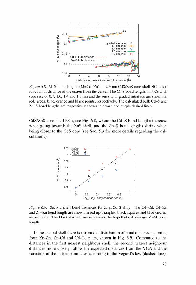
Cd S bulk distanceZn S bulk distance
2.25
2.3
2.35
2.4
2.45
0 2 4 6 8 10 12 14
MS
bond le
ngth
(Å
)
distance of the cations from the center (Å)
graded interface1.8 nm core1.4 nm core1.0 nm core0.7 nm core
Figure 6.8. M–S bond lengths (M=Cd, Zn), in 2.9 nm CdS/ZnS core-shell NCs, as a
function of distance of the cation from the center. The M–S bond lengths in NCs with
core size of 0.7, 1.0, 1.4 and 1.8 nm and the ones with graded interface are shown in
red, green, blue, orange and black points, respectively. The calculated bulk Cd–S and
Zn–S bond lengths are respectively shown in brown and purple dashed lines.
CdS/ZnS core-shell NCs, see Fig. 6.8, where the Cd–S bond lengths increase
when going towards the ZnS shell, and the Zn–S bond lengths shrink when
being closer to the CdS core (see Sec. 5.3 for more details regarding the cal-
culations).
3.75
3.8
3.85
3.9
3.95
4
4.05
0 0.2 0.4 0.6 0.8 1
M−
M d
ista
nces
(Å
)
Zn1−xCdxS alloy composition (x)
Cd−CdCd−ZnZn−Zn
Figure 6.9. Second shell bond distances for Zn1-xCdxS alloy. The Cd–Cd, Cd–Zn
and Zn–Zn bond length are shown in red up-triangles, black squares and blue circles,
respectively. The black dashed line represents the hypothetical average M–M bond
length.
In the second shell there is a trimodal distribution of bond distances, coming
from Zn-Zn, Zn-Cd and Cd-Cd pairs, shown in Fig. 6.9. Compared to the
distances in the first nearest neighbour shell, the second nearest neighbour
distances more closely follow the expected distances from the VCA and the
variation of the lattice parameter according to the Vegard’s law (dashed line).
77
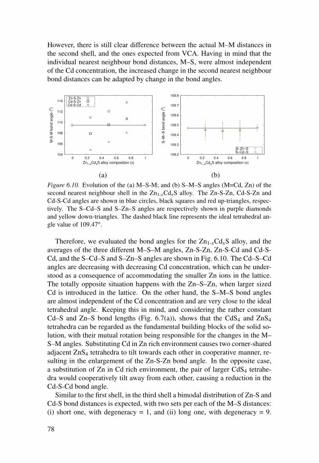
However, there is still clear difference between the actual M–M distances in
the second shell, and the ones expected from VCA. Having in mind that the
individual nearest neighbour bond distances, M–S, were almost independent
of the Cd concentration, the increased change in the second nearest neighbour
bond distances can be adapted by change in the bond angles.
104
106
108
110
112
114
0 0.2 0.4 0.6 0.8 1
M-S
-M b
ond
angl
e (o )
Zn1-xCdxS alloy composition (x)
Zn-S-ZnCd-S-ZnCd-S-Cd
109.2
109.3
109.4
109.5
109.6
109.7
109.8
0 0.2 0.4 0.6 0.8 1
S−
M−
S b
ond
angl
e (o )
Zn1−xCdxS alloy composition (x)
S−Zn−SS−Cd−S
(a) (b)
Figure 6.10. Evolution of the (a) M–S-M; and (b) S–M–S angles (M=Cd, Zn) of the
second nearest neighbour shell in the Zn1-xCdxS alloy. The Zn-S-Zn, Cd-S-Zn and
Cd-S-Cd angles are shown in blue circles, black squares and red up-triangles, respec-
tively. The S–Cd–S and S–Zn–S angles are respectively shown in purple diamonds
and yellow down-triangles. The dashed black line represents the ideal tetrahedral an-
gle value of 109.47o.
Therefore, we evaluated the bond angles for the Zn1-xCdxS alloy, and the
averages of the three different M–S–M angles, Zn-S-Zn, Zn-S-Cd and Cd-S-
Cd, and the S–Cd–S and S–Zn–S angles are shown in Fig. 6.10. The Cd–S–Cd
angles are decreasing with decreasing Cd concentration, which can be under-
stood as a consequence of accommodating the smaller Zn ions in the lattice.
The totally opposite situation happens with the Zn–S–Zn, when larger sized
Cd is introduced in the lattice. On the other hand, the S–M–S bond angles
are almost independent of the Cd concentration and are very close to the ideal
tetrahedral angle. Keeping this in mind, and considering the rather constant
Cd–S and Zn–S bond lengths (Fig. 6.7(a)), shows that the CdS4 and ZnS4
tetrahedra can be regarded as the fundamental building blocks of the solid so-
lution, with their mutual rotation being responsible for the changes in the M–
S–M angles. Substituting Cd in Zn rich environment causes two corner-shared
adjacent ZnS4 tetrahedra to tilt towards each other in cooperative manner, re-
sulting in the enlargement of the Zn-S-Zn bond angle. In the opposite case,
a substitution of Zn in Cd rich environment, the pair of larger CdS4 tetrahe-
dra would cooperatively tilt away from each other, causing a reduction in the
Cd-S-Cd bond angle.
Similar to the first shell, in the third shell a bimodal distribution of Zn-S and
Cd-S bond distances is expected, with two sets per each of the M–S distances:
(i) short one, with degeneracy = 1, and (ii) long one, with degeneracy = 9.
78
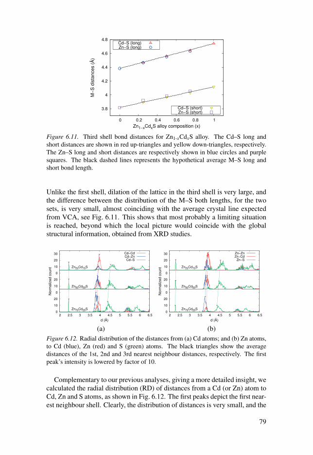
3.8
4
4.2
4.4
4.6
4.8
0 0.2 0.4 0.6 0.8 1
MS
dis
tan
ces
(Å)
Zn1 xCdxS alloy composition (x)
Cd S (long)Zn S (long)
Cd S (short)Zn S (short)
Figure 6.11. Third shell bond distances for Zn1-xCdxS alloy. The Cd–S long and
short distances are shown in red up-triangles and yellow down-triangles, respectively.
The Zn–S long and short distances are respectively shown in blue circles and purple
squares. The black dashed lines represents the hypothetical average M–S long and
short bond length.
Unlike the first shell, dilation of the lattice in the third shell is very large, and
the difference between the distribution of the M–S both lengths, for the two
sets, is very small, almost coinciding with the average crystal line expected
from VCA, see Fig. 6.11. This shows that most probably a limiting situation
is reached, beyond which the local picture would coincide with the global
structural information, obtained from XRD studies.
0
10
20
0
10
20
0
10
20
30
2 2.5 3 3.5 4 4.5 5 5.5 6 6.5
Nor
mal
ized
cou
nt
d (Å)
Zn75Cd25S
Zn50Cd50S
Zn25Cd75S
Cd−CdCd−ZnCd−S
0
10
20
0
10
20
0
10
20
30
2 2.5 3 3.5 4 4.5 5 5.5 6 6.5
Nor
mal
ized
cou
nt
d (Å)
Zn75Cd25S
Zn50Cd50S
Zn25Cd75S
Zn−ZnZn−Cd
Zn−S
(a) (b)
Figure 6.12. Radial distribution of the distances from (a) Cd atoms; and (b) Zn atoms,
to Cd (blue), Zn (red) and S (green) atoms. The black triangles show the average
distances of the 1st, 2nd and 3rd nearest neighbour distances, respectively. The first
peak’s intensity is lowered by factor of 10.
Complementary to our previous analyses, giving a more detailed insight, we
calculated the radial distribution (RD) of distances from a Cd (or Zn) atom to
Cd, Zn and S atoms, as shown in Fig. 6.12. The first peaks depict the first near-
est neighbour shell. Clearly, the distribution of distances is very small, and the
79
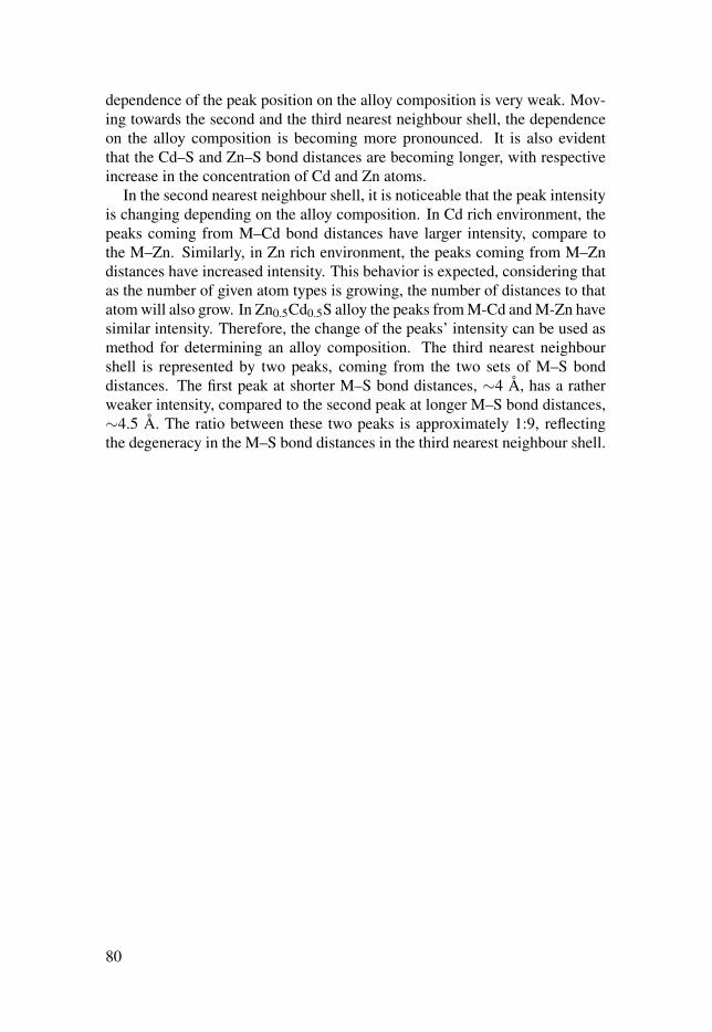
dependence of the peak position on the alloy composition is very weak. Mov-
ing towards the second and the third nearest neighbour shell, the dependence
on the alloy composition is becoming more pronounced. It is also evident
that the Cd–S and Zn–S bond distances are becoming longer, with respective
increase in the concentration of Cd and Zn atoms.
In the second nearest neighbour shell, it is noticeable that the peak intensity
is changing depending on the alloy composition. In Cd rich environment, the
peaks coming from M–Cd bond distances have larger intensity, compare to
the M–Zn. Similarly, in Zn rich environment, the peaks coming from M–Zn
distances have increased intensity. This behavior is expected, considering that
as the number of given atom types is growing, the number of distances to that
atom will also grow. In Zn0.5Cd0.5S alloy the peaks from M-Cd and M-Zn have
similar intensity. Therefore, the change of the peaks’ intensity can be used as
method for determining an alloy composition. The third nearest neighbour
shell is represented by two peaks, coming from the two sets of M–S bond
distances. The first peak at shorter M–S bond distances, ∼4 Å, has a rather
weaker intensity, compared to the second peak at longer M–S bond distances,
∼4.5 Å. The ratio between these two peaks is approximately 1:9, reflecting
the degeneracy in the M–S bond distances in the third nearest neighbour shell.
80

7. Summary and outlook
The material research is becoming a dominant part in many aspects of science
and technology, providing valuable new and innovative ideas and applications.
In many occasions the experimental findings are supported by density func-
tional theory (DFT) calculations. Sometimes the DFT provides a more funda-
mental understanding of the various experimentally observed phenomena, and
in a number of cases, manages to predict certain behaviour of a material under
given conditions. The DFT is proven to be an essential tool in understanding
and describing materials and physical processes. Interestingly, in variety of
circumstances, even the most basic DFT approximations can give a good es-
timate of the experimentally observed characteristics. However, the standard
exchange correlation potentials (LDA and GGA), as the ones employed in the
present calculations, have many shortcoming when it comes to predicting band
gaps, as well as optical and transport properties. Therefore, for more complete
and accurate studies, the use of more accurate theoretical methods is crucial.
Hence, naturally the next step would be to extend the studies presented in this
thesis by employing methods based on many-body perturbation theory (GW,
BSE) or using an exact description of the Hartree-Fock exchange.
Central part in this thesis occupies the study of silicon nanocrystals (Si
NCs). Therefore, understanding the morphology of the Si NCs, before per-
forming any calculations is crucial. Based on the comparison of the cohesive
energies and the electronic properties of Si NCs with various shapes, spher-
ical and NCs with Wulff shape, the spherical NCs were chosen as suitable
model for further calculations. For the spherical Si NCs, we observed gradual
merging of the HOMO-LUMO gap and the optical absorption gap with de-
creasing NC size, indicating a transition from indirect to direct band gap. This
transition in the band gap character was correlated with the changes in the
highest occupied (HOMO) and lowest unoccupied (LUMO) eigenstates wave-
functions (WFs), where gradual emergence of bulk-like k selection rule with
increasing NCs size is evident. This shows that there is an increased proba-
bility of direct transitions in smaller Si NCs, highlighting the importance of
confining the size of Si for light-emitting applications. It was furthermore
shown that the electronic and optical properties of the Si NCs are influenced
significantly more by double-bonded impurities on the surface, compared to
single-bonded impurities. The modification in the properties comes from the
increased localisation of the HOMO and LUMO WFs around the surface im-
purity, which localisation decreases with growing NC size. This change in the
localisation causes transformation of the symmetry of the states, making the
81

optical transitions between the states more probable, compared to the ones in
fully hydrogenated Si NCs. In this study, the effect of a single impurity on the
surface was investigated, however in experiments higher number of impurities
are present. Therefore, it is necessary to study the influence of multiple im-
purities on the surface of Si NCs on the electronic and the optical properties.
This is especially important for NCs larger than 2 nm, for which the effect of
the double-bonded impurities dissipates, as we have shown in our study.
Furthermore, the different capping ligands have distinct influence on the
electronic and optical properties of the Si NCs, which comes from the differ-
ence in the functional group of the ligand. The difference in the ligands also
reflects in the radiative lifetimes, where the radiative lifetimes of ethylamine-
capped NCs depend more weakly on the NC size compared to the CH3-capped
NCs. The similarity in the radiative lifetimes of ethylamine-capped NCs was
assigned to the rather constant symmetry of the HOMO WF in the capped NCs
with changes in the NC size. However, the contribution to the states around
the gap from the two considered ligands, methyl and ethylamine, is differ-
ent. Thus, it would be instructive to investigate the influence of ligands with
various functional groups (e.g. –OH, –SH, –Cl, –COOH etc.) on the radia-
tive lifetimes. Considering that the spatial separation between the functional
group and the active Si NC core can affect the radiative lifetimes, it is also
worth studying the effect of the ligands with different lengths of the carbon
chain. The Si NCs are also considered to be an important component of the
new generation of solar cells, because once embedded in a host matrix, the
possibility of charge separation is increased, giving rise to higher efficiency.
We demonstrated that in a system composed of Si NC in a SiC host matrix,
type-II band alignment is formed, allowing for spatial separation of the charge
carriers, with the top of the valence band being in the NC and the bottom of
the conduction band in the host matrix. The positions of the band maxima
can be interchanged by introducing oxygen, which explains the lowering of
the dark conductivity in Si NCs embedded in amorphous SiC upon insertion
of oxygen. Moreover, a leakage of valence band states between neighbouring
NCs is observed, when the NC-NC distance is less than 1.7 nm. In a contin-
uation of this study, an amorphous SiC can be considered as a more realistic
model of the SiC host matrix. In addition, other host matrices with smaller
band gap compared to the widely used matrices, for example ZnO or ITO, can
be examined to see if they can also provide similar charge separation, as in the
studied system, giving the possibility of producing more efficient solar cells.
For all of these complex systems the transport properties can be calculated,
yielding a deeper insight into their applicability as photovoltaics.
Great deal of attention has also been devoted to the understanding of the
influence of the size and different structural models on the electronic and op-
tical properties of CdSe/CdS and CdS/ZnS core-shell NCs. We show a similar
behaviour of the band gaps in both CdSe/CdS and CdS/ZnS core-shell NCs,
with variation in the size and the structural model, where the band gaps of the
82

CdS/ZnS NCs are influenced more by the structural changes. In both types
of core-shell NCs, the confinement of the HOMO WF in the core of the NC
with same size is similar, regardless of the structural model, indicating a simi-
lar Auger rates in both types of NCs, hence similar quantum efficiency (QE).
However, the LUMO WF in the CdSe/CdS NCs spreads more in the shell of
the NC, compared to the LUMO WF of the CdS/ZnS NC. This different spa-
tial distribution of the HOMO and LUMO WF influences both the radiative
lifetimes and the electron-hole Coulomb interaction energies (e-h Eb). The
relative difference in the radiative lifetimes in both types of NCs is signifi-
cantly smaller compared to the relative difference in the e-h Eb. Furthermore,
the e-h Eb in the CdSe/CdS NCs are considerably smaller than in the CdS/ZnS.
The decrease in the e-h Eb can lower the Auger rates, increasing the QE, which
can be one of the reasons for the distinct photoluminescence properties of the
CdSe/CdS and CdS/ZnS NCs. Keeping this in mind, to increase the QE of
the CdS/ZnS NCs, the structure should be designed to allow the LUMO WF
to spread more in the ZnS shell. This can be achieved by introducing alloyed
interface, i.e. forming CdS/Zn1-xCdxS/ZnS NCs, with the spatial distribution
of the LUMO WF being naturally dependent on the concentration of the Cd
atoms. The changes in the spread of the LUMO WF would induce changes
in the properties of the CdS/Zn1-xCdxS/ZnS NCs, which can be an interesting
topic for further study.
Beside being the most useful tool in estimating and predicting the funda-
mental electronic structure properties, DFT can be used in modelling of var-
ious materials. We show that the ripples in graphene, grown on Fe(110) sur-
face, can be well reproduced by DFT calculations. The experience gained
from this study can be applied in modelling the growth of graphene on other
surfaces, which can be further used in calculating various properties, or simu-
lating epitaxial growth. Moreover, the local order in Zn1-xCdxS alloys can be
also well estimated, showing that the Cd–S and Zn–S bond distances in the
first nearest neighbour shell of the alloy are very close to the ones in pure CdS
and ZnS. This local picture changes when going towards higher neighbouring
shells, with the Cd–S and Zn–S bond distances in third nearest neighbour shell
becoming almost identical to the distances expected from XRD. In that study,
random position of the cations were considered in the models. However, it is
worth investigating if there are any preferential orientations in which the atoms
in the Zn1-xCdxS alloy would arrange, and compare this to different alloys. In
addition, the study can be extended to investigating the interface between ZnS
and CdS or other similar materials, along different crystallographic planes.
83

8. Sammanfattning
En grundläggande förståelse för processer och egenskaper hos material på
en atomnivå är avgörande för att utveckla den moderna materialforskningen.
Detta kan realiseras genom en kvantmekanisk beskrivning av växelverkan
mellan atomer och elektroner i materialen. Den huvudsakliga vägen till en-
ergier och krafter mellan atomer samt en beskrivning av bindningen mellan
dem är att lösa den grundläggande kvantmekaniska ekvationen, Schrödin-
gerekvationen. För ett flerelektronsystem är en analytisk lösning av Schrödin-
gerekvationen dock otillgänglig, varför ett flertal numeriska tillvägagångssätt
för att noggrant och effektivt lösa ekvationen utvecklats. Ett genombrott i
detta arbete var utvecklingen av en teori som erhåller flerelektronsystemets
grundtillstånd via elektrontätheten, nämligen täthetsfunktionalteori (DFT).
Inom DFT behandlas de mer svårtillgängliga delarna av elektron-elektron-
växelverkan inom en effektiv utbytesväxelverkan-korrelationsfunktional, vil-
ket ger en noggrann lösning till Schrödingerekvationen om dess exakta form
är känd. Tyvärr är den exakta utbytesväxelverkan-korrelationsfunktionalen ej
känd och approximationer måste tillämpas. Trots dessa approximationer har
DFT varit framgångsrikt i att beskriva många material. Denna avhandling
fokuserar på aspekter av tillämpbarhet hos DFT i att beskriva diverse materi-
alegenskaper samt modellering av olika material. Innan en översikt av erhållna
resultat presenteras ges en kort introduktion av betydelsen hos de studerade
systemen.
Områdena nanovetenskap och nanoteknologi har blivit ledande inom de-
sign av nya och innovativa material vilka kan användas inom en bredd av
tekniska användningsområden. De enklare och billigare metoderna att pro-
ducera nanokristaller som kan avge högintensivt ljus i ett smalt spektralom-
fång har resulterat i växande användning av nanokristaller i fotovoltaiska samt
optoelektroniska tillämpningsområden. Nanokristaller kan numera hittas i
LEDs, lasrar, solceller, enfotonkällor och även i biomedicinska tillämpningar
för avbildning och märkning. De utmärka ljusavgivningsegenskaperna hos
nanokristaller är ett resultat av Kvantbundenhet vilket uppstår på grund av ma-
terialets storlek. När nanokristaller bildas blir excitonerna (elektron-hålparen
vilka leder till ljusemissionen) instängda vilket leder till högre rekombination-
shastigheter och ökad fotoluminescensintensitet. Minskad storlek hos nano-
kristaller leder också till högre energi hos emitterat ljus vilket tillåter fotolu-
minescensegenskaperna att ändras enligt specifika krav genom att ändra nano-
kristaller storlek.
84

Den exceptionella fotoluminescensen hos nanokristaller kan ändras avsevärt
beroende på omgivning och i synnerhet nanokristallernas ytmaterial. Ytoren-
heter kan introducera medelgaptillstånd vilka stänger in elektroner eller hål
och underlättar andra ickeradiativa rekombinationsprocesser. Dessa processer
minskar fotoluminescensintensiteten och i leder i vissa fall till ett skift i ener-
gin hos det avgivna ljuset. För att undvika den bristen kapslas nanokristaller-
nas yta så att full passivitet hos ensamt electronpar försäkras. Detta kan
uppnås genom att täcka nanokristallerna med andra halvledare vilket leder
till så kallade kärna-skal nanokristaller1. Denna typ av ytpassivation är i
synnerhet viktig för II-IV halvledare där excitoner också kan stängas in i
nanokristallernas kärna och på så sätt minska yteffekter. I andra typer av
halvledarnanokristaller av t.ex. Si kan ytan passiveras med organiska moleky-
ler vilka dämpar oxideringen på ytan och ökar fotoluminescensintensiteten.
Utöver ljusemissionstillämpningar så kan kvanteffekter relaterade till nano-
kristallernas storlek användas i solcellssyfte. I det fallet måste nanokristallerna
inneslutas i en värdmatris vilken agerar som laddningsbärare. I denna typ
av komplext system ökar ljusomvandlingseffektiviteten med spatial separation
och ökad mobilitet hos laddningsbärarna.För produktion av effektiva solceller
måste kraven på dessa egenskaper därför uppfyllas.
Med allt detta i åtanke avser vi att studera elektroniska samt optiska egen-
skaper hos kärna-skal och Si-nanokristaller genom användning av DFT. Vi
betraktar CdSe/CdS och CdS/ZnS kärna-skal nanokristaller med olika stor-
lek samt olika strukturmodeller. som väntat från kvantbundenhetseffekter ob-
serveras en breddning av bandgapet med minskad storled hos nanokristallerna.
Olika strukturmodeller finnes dock endast leda till små skillnader i bandgap
såväl som tillståndstäthet och absorptionsindex. I en fördjupning av våra in-
sikter inser vi att strålningslivstiderna och interaktionsenergierna mellan elek-
troner och hål påvisar något större skillnader för olika strukturmodeller. Detta
stämmer väl med experimentella resultat vilka visar att legerade eller grader-
ade gränsskikt kan minska Augertakten och att CdSe/CdS nanokristaller bör
ha högre kvanteffektivitet.
Vidare fokuserade vi på förståelse för fotoluminescensen hos hydrogen-
erade Si-nanokristaller genom att studera storleksutvecklingen hos HOMO-
LUMO och det optiska absorptionsgapet. Vi observerar sammanfogning av
gapen i de minsta studerade nanokristallerna vilket indikerar en möjlig ökn-
ing av antalet direkta övergångar med minskande storlek hos nanokristallerna.
Detta förklarades i mer detalj genom studier av k rymdsprojektioner av HOMO
och LUMO-vågfunktionerna. Studien av Si-nanokristaller utökades genom en
undersökning av inflytandet hos enstaka orenheter på ytan av de hydrogener-
ade Si-nanokristallerna på deras elektroniska och optiska egenskaper. Vi visar
att dubbelbundna orenheter inducerar avsevärt större ändringar i dessa egen-
skaper jämfört med enkelbundna orenheter för nanokristaller upp till 2.5 nm.
1The translation into English would be core-shell nanocrystals.
85
Dessa skillnader mellan enkel och dubbelbundna orenheter påvisades också
i karaktären hos tillstånden runt gapet och hos HOMO och LUMO-vågfunkti-
onerna. Utöver detta kapslade vi också Si-nanokristallernas ytor med två olika
typer av organiska liggandes i syfte att studera deras fotoluminescensegen-
skaper. Vi visar att ökad storlek hos nanokristallerna leder till mindre bandgap
och lägre övergångstakt. Vidare visar vi att hål kan fångas in vid NH2-gruppen
hos aminliganden, vilket förklarar den lägre fotoluminescensintensiteten i
aminkapslade Si-nanokristaller. Slutligen har vi studerat inflytandet hos grän-
sskikt på banduppriktningen i Si-nanokristaller inbäddade i SiC och beroendet
hos vågfunktionens läckage på avstånd mellan närliggande Si-nanokristaller
diskuteras. När avståndet mellan närliggande nanokristaller är mindre än 1.7
nm observeras läckage av laddningstäthet mellan närliggande Si-nanokristaller.
Dessutom visar vi att tillsatt syre vid gränsskiktet mellan Si-nanokristaller och
SiC-matrisen orsakar att bandkanten vänder sin position i systemet. Vi re-
laterar detta utbyte i banduppriktningen med experimentellt lägre observerad
mörk ledningsförmåga när syre introduceras i ett system av Si-nanokristaller
samt SiC.
En annan del av avhandlingen behandlar förmågan hos DFT att modellera
olika material. Sedan upptäckten av grafen och efter att det påvisats att ma-
terialet uppvisar högst önskvärda egenskaper, har stor ansträngning riktats åt
att producera plan grafen till lägre pris. Sen det visades att plan grafen Kan
tillverkas på en yta Fe(110) har vårt mål varit att stödja denna experimentella
upptäckt genom modellering av tillväxt av grafen på Fe(110) med fokus på
krusningar hos grafenet. Vi visar att grafen kemisorberas på Fe(110) och vi
reproducerar den experimentellt observerade krusningsamplituden. Förmå-
gan hos DFT att pålitligt modellera strukturella egenskaper hos bulkmaterial
påvisades också hos Zn1-xCdxS-legeringar. Konceptet kemiskt tryck och den
så kallade virtuella kristallapproximationen, båda härledda från makroskopiska
observationer, utforskades för Zn1-xCdxS-legeringar med hjälp av experimen-
tella metoder för att undersöka den lokala mikroskopiska strukturen. Innan
erhållande av experimentella resultat, förutsade vi avstånd mellan närmaste
grannar samt bindningsvinklar baserat på DFT i Zn1-xCdxS-legeringar.
86

Acknowledgements
I would like to express my deepest appreciation to my main supervisor, Ján
Rusz, for his excellent guidance, patience, and continuous conveyed spirit of
adventure in regard to research and scholarship. His motivation, enthusiasm
and immense knowledge were constantly pushing me to strive for excellence,
and without his endless help this thesis would not be possible. I owe my deep-
est gratitude to my second supervisor, Olle Eriksson, for sharing his wisdom,
the insightful comments and suggestions, the encouragement to always look
for new and innovative ideas, and to continually deepen the understanding of
the problem in hand.
I cannot find words to express my gratitude to my family for their bound-
less love and support. The encouragement and motivation that I continuously
received from them is the perpetual fuel that makes me always move forward.
My most sincere thanks to my office mates, Sumanta and Soumyajyoti, for
their spontaneous jokes, lovely discussions, perceptive comments and putting
up with me for all this time. My gratitude is extended to Pablo, Ana, Marco,
Jonathan, Sara, Iulia, Sumanta, and Naum, for the great game nights, the won-
derful get-togethers, the support in any crazy idea and the willingness to have
a drink in the evenings.
To my colleagues, Barbara, Beatriz, Yaroslav, Ritwik, Marcio, Ralph, Li
Wen, Manuel, Pablo, Jonathan, Marco, Heike, Raghuveer, Igor, Johan, Inka,
Attila, Corina, Mirek, Adam, Karel, Kostas, Anna, Rodrigo, Marco(2), Sara,
Alex, Iulia, Debora, Leyla, Sumanta, Soumyajyoti, Carmine, and many others,
I want to express my gratitude for all spontaneous coffee breaks, discussions
during lunch, evenings out and various activities; the time spent with you was
time well spent. I have also been fortunate to be part of the small, but dy-
namic Macedonian group. Aleksandra, Naum, Jordan, Jane, Elena, Dushko
and Sanja with Jan, though the dynamics of research life has allowed us to
be compact for relatively short time, every moment together was enjoyable,
always reminding me of the roots, and I am thankful for that.
I am greatly indebted to my previous advisor Ljupco Pejov for providing me
with the basic knowledge in the filed of DFT studies and showing me the true
value of fundamental science. I am grateful to Alex for his extensive help in
translating the thesis summary in Swedish. It is definitely, without any doubt
worth mentioning my proof-reading buddies, Pablo, Mirek, Iulia, Soumyajyoti
and Jordan to whom I am truly thankful for their help in improving this thesis.
Special thanks to my traveling companions, Biljana, Sumanta and Soumya-
jyoti for joining me in various adventures, letting me organise the trips and
87

silently endure the bustling schedules. I also should not forget to thank my
flatmate/landlord Thomas for giving a wonderful place to live and who was
peacefully struggling with the mess called Vancho for more than four years. I
would like to thank my dance partner, Daniela, for the great time spent together
practicing and competing, and to my dance teacher, Galina, who showed me
the beauty of ballroom dances and kept my passion for dancing alive.
88

References
[1] H. A. Lorentz, The theory of electrons and its applications to the phenomenaof light and radiant, 2nd ed. (Leipzig: B.G. Teubner; New York: G.E. Stechert,
1916).
[2] P. Zeeman, Nature 55, 347 (1897).
[3] F. Braun, Ann. Phys. (Berlin) 296, 552 (1897).
[4] J. J. Thomson, Philos. Mag. Series 5 44, 293 (1897).
[5] H. Geiger and E. Marsden, Proc. Math. Phys. Eng. Sci. 82, 495 (1909).
[6] N. Bohr, Philos. Mag. Series 6 26, 1 (1913).
[7] N. Bohr, Philos. Mag. Series 6 26, 476 (1913).
[8] N. Bohr, Philos. Mag. Series 6 26, 857 (1913).
[9] M. Planck, Ann. Phys. (Berlin) 309, 553 (1901).
[10] A. Einstein, Ann. Phys. (Berlin) 322, 132 (1905).
[11] O. Stern, Z. Phys. 7, 249 (1921).
[12] W. Gerlach and O. Stern, Z. Phys. 8, 110 (1922).
[13] W. Gerlach and O. Stern, Z. Phys. 9, 349 (1922).
[14] M. Born and P. Jordan, Z. Phys. 34, 858 (1925).
[15] W. Heisenberg, Z. Phys. 33, 879 (1925).
[16] M. Born, W. Heisenberg, and P. Jordan, Z. Phys. 35, 557 (1926).
[17] E. Schrödinger, Ann. Phys. (Berlin) 384, 361 (1926).
[18] E. Schrödinger, Ann. Phys. (Berlin) 384, 489 (1926).
[19] E. Schrödinger, Ann. Phys. (Berlin) 385, 437 (1926).
[20] E. Schrödinger, Ann. Phys. (Berlin) 386, 109 (1926).
[21] J. Pauli, W., Z. Phys. 43, 601 (1927).
[22] P. A. M. Dirac, Proc. Math. Phys. Eng. Sci. 118, 351 (1928).
[23] P. A. M. Dirac, Proc. Math. Phys. Eng. Sci. 117, 610 (1928).
[24] D. R. Hartree, Math. Proc. Cambridge 24, 89 (1928).
[25] V. Fock, Z. Phys. 61, 126 (1930).
[26] J. C. Slater, Phys. Rev. 35, 210 (1930).
[27] K. A. Brueckner, Phys. Rev. 97, 1353 (1955).
[28] K. A. Brueckner, Phys. Rev. 100, 36 (1955).
[29] J. Goldstone, Proc. Math. Phys. Eng. Sci. 239, 267 (1957).
[30] W. L. McMillan, Phys. Rev. 138, A442 (1965).
[31] R. C. Grimm and R. G. Storer, J. Comput. Phys. 7, 134 (1971).
[32] J. B. Anderson, J. Chem. Phys. 63, 1499 (1975).
[33] J. B. Anderson, J. Chem. Phys. 65, 4121 (1976).
[34] P. Hohenberg and W. Kohn, Phys. Rev. 136, B864 (1964).
[35] W. Kohn and L. J. Sham, Phys. Rev. 140, A1133 (1965).
[36] P. Ordejón, E. Artacho, and J. M. Soler, Phys. Rev. B 53, R10441 (1996).
[37] J. M. Soler, E. Artacho, J. D. Gale, A. García, J. Junquera, P. Ordejón, and
D. Sánchez-Portal, J. Phys. Condens. Matter 14, 2745 (2002).
89
[38] F. Trani, G. Cantele, D. Ninno, and G. Iadonisi, Phys. Rev. B 72, 075423
(2005).
[39] M. V. Wolkin, J. Jorne, P. M. Fauchet, G. Allan, and C. Delerue, Phys. Rev.
Lett. 82, 197 (1999).
[40] M. Born and R. Oppenheimer, Ann. Phys. (Berlin) 389, 457 (1927).
[41] L. H. Thomas, Math. Proc. Cambridge 23, 542 (1927).
[42] E. Fermi, Math. Proc. Cambridge 6, 602 (1927).
[43] P. A. M. Dirac, Math. Proc. Cambridge 26, 376 (1930).
[44] D. M. Ceperley and B. J. Alder, Phys. Rev. Lett. 45, 566 (1980).
[45] J. P. Perdew, J. A. Chevary, S. H. Vosko, K. A. Jackson, M. R. Pederson, D. J.
Singh, and C. Fiolhais, Phys. Rev. B 46, 6671 (1992).
[46] J. P. Perdew and W. Yue, Phys. Rev. B 33, 8800 (1986).
[47] F. Bloch, Z. Phys. 52, 555 (1929).
[48] D. R. Hamann, M. Schlüter, and C. Chiang, Phys. Rev. Lett. 43, 1494 (1979).
[49] N. Troullier and J. L. Martins, Phys. Rev. B 43, 1993 (1991).
[50] L. Kleinman and D. M. Bylander, Phys. Rev. Lett. 48, 1425 (1982).
[51] J. C. Slater, Phys. Rev. 36, 57 (1930).
[52] S. F. Boys, Proc. Math. Phys. Eng. Sci. 200, 542 (1950).
[53] L. T. Canham, Appl. Phys. Lett. 57, 1046 (1990).
[54] R. J. Walters, G. I. Bourianoff, and H. A. Atwater, Nat. Mater. 4, 143 (2005).
[55] K. D. Hirschman, L. Tsybeskov, S. P. Duttagupta, and P. M. Fauchet, Nature
384, 338 (1996).
[56] K.-Y. Cheng, R. Anthony, U. R. Kortshagen, and R. J. Holmes, Nano Lett. 11,
1952 (2011).
[57] F. Maier-Flaig, J. Rinck, M. Stephan, T. Bocksrocker, M. Bruns, C. Kübel,
A. K. Powell, G. A. Ozin, and U. Lemmer, Nano Lett. 13, 475 (2013).
[58] M. Ghulinyan, D. Navarro-Urrios, A. Pitanti, A. Lui, G. Pucker, and L. Pavesi,
Opt. Express 16, 13218 (2008).
[59] J. R. RodrÃguez, J. G. C. Veinot, P. Bianucci, and A. Meldrum, Appl. Phys.
Lett. 92, 131119 (2008).
[60] V. Švrcek, A. Slaoui, and J.-C. Muller, Thin Solid Films 451-452, 384 (2004).
[61] G. Conibeer, M. Green, R. Corkish, Y. Cho, E.-C. Cho, C.-W. Jiang,
T. Fangsuwannarak, E. Pink, Y. Huang, T. Puzzer, T. Trupke, B. Richards,
A. Shalav, and K. lung Lin, Thin Solid Films 511-512, 654 (2006).
[62] D. Song, E.-C. Cho, G. Conibeer, C. Flynn, Y. Huang, and M. A. Green, Sol.
Energ. Mat. Sol. 92, 474 (2008).
[63] M. Govoni, I. Marri, and S. Ossicini, Nat. Photon. 6, 672 (2012).
[64] Z. F. Li and E. Ruckenstein, Nano Lett. 4, 1463 (2004).
[65] F. Erogbogbo, K.-T. Yong, I. Roy, G. Xu, P. N. Prasad, and M. T. Swihart,
ACS Nano 2, 873 (2008).
[66] J.-H. Park, L. Gu, G. von Maltzahn, E. Ruoslahti, S. N. Bhatia, and M. J.
Sailor, Nat. Mater. 8, 331 (2009).
[67] Y. Zhong, F. Peng, F. Bao, S. Wang, X. Ji, L. Yang, Y. Su, S.-T. Lee, and
Y. He, J. Am. Chem. Soc. 135, 8350 (2013).
[68] E. Borsella, R. D’Amato, M. Falconieri, E. Trave, A. Panariti, and I. Rivolta,
J. Mater. Res. 28, 193 (2013).
90

[69] S. Chan, Y. Li, L. J. Rothberg, B. L. Miller, and P. M. Fauchet, Mater. Sci.
Eng. C 15, 277 (2001).
[70] L. Rebohle, T. Gebel, R. Yankov, T. Trautmann, W. Skorupa, J. Sun,
G. Gauglitz, and R. Frank, Opt. Matter. 27, 1055 (2005).
[71] M. Brandt, H. Fuchs, M. Stutzmann, J. Weber, and M. Cardona, Solid State
Commun. 81, 307 (1992).
[72] S. Schuppler, S. L. Friedman, M. A. Marcus, D. L. Adler, Y.-H. Xie, F. M.
Ross, T. D. Harris, W. L. Brown, Y. J. Chabal, L. E. Brus, and P. H. Citrin,
Phys. Rev. Lett. 72, 2648 (1994).
[73] J. von Behren, T. van Buuren, M. Zacharias, E. Chimowitz, and P. Fauchet,
Solid State Commun. 105, 317 (1998).
[74] T. van Buuren, L. N. Dinh, L. L. Chase, W. J. Siekhaus, and L. J. Terminello,
Phys. Rev. Lett. 80, 3803 (1998).
[75] A. Nozik, Physica E 14, 115 (2002).
[76] G. J. Conibeer, C.-W. Jiang, D. König, S. Shrestha, T. Walsh, and M. A.
Green, Thin Solid Films 516, 6968 (2008).
[77] Y. Kurokawa, S. Yamada, S. Miyajima, A. Yamada, and M. Konagai, Current
Applied Physics 10, S435 (2010).
[78] J. Barbé, L. Xie, K. Leifer, P. Faucherand, C. Morin, D. Rapisarda, E. D. Vito,
K. Makasheva, B. Despax, and S. Perraud, Thin Solid Films 522, 136 (2012).
[79] S. Perraud, E. Quesnel, S. Parola, J. Barbé, V. Muffato, P. Faucherand,
C. Morin, K. Jarolimek, R. A. C. M. M. Van Swaaij, M. Zeman, S. Richards,
A. Kingsley, H. Doyle, K. Linehan, S. O’Brien, I. M. Povey, M. E. Pemble,
L. Xie, K. Leifer, K. Makasheva, and B. Despax, Phys. Status Solidi A 210,
649 (2013).
[80] H.-C. Weissker, J. Furthmüller, and F. Bechstedt, Phys. Rev. B 65, 155328
(2002).
[81] S. Furukawa and T. Miyasato, Phys. Rev. B 38, 5726 (1988).
[82] I. Vasiliev, S. Ögüt, and J. R. Chelikowsky, Phys. Rev. Lett. 86, 1813 (2001).
[83] Y. Wang, C. Chen, Z. Wu, W. Liang, X. Wang, X. Ding, L. Chu, Z. Deng, and
G. Chen, Jinzhong Fu, Micro & Nano Lett. 6, 1 (2011).
[84] C. Delerue, M. Lannoo, and G. Allan, Phys. Rev. Lett. 84, 2457 (2000).
[85] T. Takagahara and K. Takeda, Phys. Rev. B 46, 15578 (1992).
[86] V. L. Colvin, M. C. Schlamp, and A. P. Alivisatos, Nature 370, 354 (1994).
[87] S. Coe, W.-K. Woo, M. Bawendi, and V. Bulovic, Nature 420, 800 (2002).
[88] N. Tessler, V. Medvedev, M. Kazes, S. Kan, and U. Banin, Science 295, 1506
(2002).
[89] Q. Sun, Y. A. Wang, L. S. Li, D. Wang, T. Zhu, J. Xu, C. Yang, and Y. Li, Nat.
Photon. 1, 717 (2007).
[90] J. M. Caruge, J. E. Halpert, V. Wood, V. Bulovic, and M. G. Bawendi, Nat.
Photon. 2, 247 (2008).
[91] V. I. Klimov, A. A. Mikhailovsky, S. Xu, A. Malko, J. A. Hollingsworth, C. A.
Leatherdale, H.-J. Eisler, and M. G. Bawendi, Science 290, 314 (2000).
[92] R. Vogel, P. Hoyer, and H. Weller, J. Phys. Chem. 98, 3183 (1994).
[93] S. A. McDonald, G. Konstantatos, S. Zhang, P. W. Cyr, E. J. D. Klem,
L. Levina, and E. H. Sargent, Nat. Mater. 4, 138 (2005).
91
[94] M. Bruchez, M. Moronne, P. Gin, S. Weiss, and A. P. Alivisatos, Science 281,
2013 (1998).
[95] W. C. W. Chan and S. Nie, Science 281, 2016 (1998).
[96] J. van Embden, J. Jasieniak, and P. Mulvaney, J. Am. Chem. Soc. 131, 14299
(2009).
[97] D. D. Sarma, A. Nag, P. K. Santra, A. Kumar, S. Sapra, and P. Mahadevan, J.
Phys. Chem. Lett. 1, 2149 (2010).
[98] Y.-S. Park, A. V. Malko, J. Vela, Y. Chen, Y. Ghosh, F. García-Santamaría,
J. A. Hollingsworth, V. I. Klimov, and H. Htoon, Phys. Rev. Lett. 106, 187401
(2011).
[99] F. García-Santamaría, S. Brovelli, R. Viswanatha, J. A. Hollingsworth,
H. Htoon, S. A. Crooker, and V. I. Klimov, Nano Lett. 11, 687 (2011).
[100] J. Zhao, O. Chen, D. B. Strasfeld, and M. G. Bawendi, Nano Lett. 12, 4477
(2012).
[101] W. K. Bae, L. A. Padilha, Y.-S. Park, H. McDaniel, I. Robel, J. M. Pietryga,
and V. I. Klimov, ACS Nano 7, 3411 (2013).
[102] O. Chen, J. Zhao, V. P. Chauhan, J. Cui, C. Wong, D. K. Harris, H. Wei, H.-S.
Han, D. Fukumura, R. K. Jain, and M. G. Bawendi, Nat. Mater. 12, 445
(2013).
[103] N. Herron, Y. Wang, and H. Eckert, J. Am. Chem. Soc. 112, 1322 (1990).
[104] J. S. Steckel, J. P. Zimmer, S. Coe-Sullivan, N. E. Stott, V. Bulovic, and M. G.
Bawendi, Angew. Chem. Int. Ed. 43, 2154 (2004).
[105] M. Protière and P. Reiss, Nanoscale Res. Lett. 1, 62 (2006).
[106] D. S. English, L. E. Pell, Z. Yu, P. F. Barbara, and B. A. Korgel, Nano Lett. 2,
681 (2002).
[107] J. H. Warner, A. Hoshino, K. Yamamoto, and R. D. Tilley, Angew. Chem. Int.
Ed. 44, 4550 (2005).
[108] M. Rosso-Vasic, E. Spruijt, B. van Lagen, L. De Cola, and H. Zuilhof, Small
4, 1835 (2008).
[109] K. Kusová, O. Cibulka, K. Dohnalová, I. Pelant, J. Valenta, A. Fucíková,
K. Žídek, J. Lang, J. Englich, P. Matejka, P. Štepánek, and S. Bakardjieva,
ACS Nano 4, 4495 (2010).
[110] S. Yang, W. Li, B. Cao, H. Zeng, and W. Cai, J. Phys. Chem. C 115, 21056
(2011).
[111] C. Delerue, G. Allan, and M. Lannoo, Phys. Rev. B 48, 11024 (1993).
[112] L.-W. Wang and A. Zunger, J. Phys. Chem. B 102, 6449 (1998).
[113] G. E. Cragg and A. L. Efros, Nano Lett. 10, 313 (2010).
[114] J. W. Haus, H. S. Zhou, I. Honma, and H. Komiyama, Phys. Rev. B 47, 1359
(1993).
[115] A. L. Efros, M. Rosen, M. Kuno, M. Nirmal, D. J. Norris, and M. Bawendi,
Phys. Rev. B 54, 4843 (1996).
[116] J. P. Wilcoxon, G. A. Samara, and P. N. Provencio, Phys. Rev. B 60, 2704
(1999).
[117] Z. Zhou, L. Brus, and R. Friesner, Nano Lett. 3, 163 (2003).
[118] K. Linehan and H. Doyle, Small 10, 584 (2014).
[119] K. S. Novoselov, A. K. Geim, S. V. Morozov, D. Jiang, Y. Zhang, S. V.
Dubonos, I. V. Grigorieva, and A. A. Firsov, Science 306, 666 (2004).
92

[120] K. S. Novoselov, A. K. Geim, S. V. Morozov, D. Jiang, M. I. Katsnelson, I. V.
Grigorieva, S. V. Dubonos, and A. A. Firsov, Nature 438, 197 (2005).
[121] Y. Zhang, Y.-W. Tan, H. L. Stormer, and P. Kim, Nature 438, 201 (2005).
[122] M. I. Katsnelson, Eur. Phys. J. B 51, 157 (2006).
[123] K. S. Novoselov, E. McCann, S. V. Morozov, V. I. Fal’ko, M. I. Katsnelson,
U. Zeitler, D. Jiang, F. Schedin, and A. K. Geim, Nat. Phys. 2, 177 (2006).
[124] M. I. Katsnelson, K. S. Novoselov, and A. K. Geim, Nat. Phys. 2, 620 (2006).
[125] J. Wintterlin and M.-L. Bocquet, Surf. Sci. 603, 1841 (2009).
[126] K. Rapcewicz, B. Chen, B. Yakobson, and J. Bernholc, Phys. Rev. B 57, 7281
(1998).
[127] G. Wulff, Z. Kristallogr. 34, 449 (1901).
[128] L. Vegard, Z. Phys. 5, 17 (1921).
[129] L. Nordheim, Ann. Phys. (Leipz.) 9, 607 (1931).
[130] L. Nordheim, Ann. Phys. (Leipz.) 9, 641 (1931).
[131] A. A. R. Fernandes, J. Santamaria, S. L. Bud’ko, O. Nakamura, J. Guimpel,
and I. K. Schuller, Phys. Rev. B 44, 7601 (1991).
[132] H. C. Nguyen and J. B. Goodenough, Phys. Rev. B 52, 324 (1995).
[133] Y. Moritomo, H. Kuwahara, Y. Tomioka, and Y. Tokura, Phys. Rev. B 55,
7549 (1997).
93

Acta Universitatis UpsaliensisDigital Comprehensive Summaries of Uppsala Dissertationsfrom the Faculty of Science and Technology 1247
Editor: The Dean of the Faculty of Science and Technology
A doctoral dissertation from the Faculty of Science andTechnology, Uppsala University, is usually a summary of anumber of papers. A few copies of the complete dissertationare kept at major Swedish research libraries, while thesummary alone is distributed internationally throughthe series Digital Comprehensive Summaries of UppsalaDissertations from the Faculty of Science and Technology.(Prior to January, 2005, the series was published under thetitle “Comprehensive Summaries of Uppsala Dissertationsfrom the Faculty of Science and Technology”.)
Distribution: publications.uu.seurn:nbn:se:uu:diva-248513
ACTAUNIVERSITATIS
UPSALIENSISUPPSALA
2015