thin-film pzt lateral actuators with extended...
TRANSCRIPT

890 JOURNAL OF MICROELECTROMECHANICAL SYSTEMS, VOL. 17, NO. 4, AUGUST 2008
Thin-Film PZT Lateral ActuatorsWith Extended Stroke
Kenn R. Oldham, Member, ASME, Jeffrey S. Pulskamp, Ronald G. Polcawich, Member, IEEE, and Madan Dubey
Abstract—Many microelectromechanical system applicationsrequire large in-plane actuation forces, with stroke lengths rangingfrom submicrometer to tens of micrometers in distance. Piezo-electric thin films are capable of generating very large actua-tion forces, but their motion is not easily directed into lateraldisplacement in microscale devices. A new piezoelectric thin-filmactuator that uses a combination of piezoelectric unimorph beamsto generate lateral displacement has been developed. The piezo-electric actuators were fabricated using chemical-solution-derivedlead zirconate titanate thin films. These actuators have demon-strated forces greater than 7 mN at displacements of nearly 1 µm,with maximum stroke lengths at 20 V greater than 5 µm ina 500-µm-long by 100-µm-wide actuator. Force and displace-ment capabilities can be manipulated through simple changesto the actuator design, while actuator nonlinearity can producedramatic gains in work capacity and stroke length for longeractuators. [2007-0298]
Index Terms—Actuators, lead zirconate titanate (PZT) ceram-ics, piezoelectric devices, robots.
I. INTRODUCTION
M ICROELECTROMECHANICAL systems (MEMS)rely upon a number of actuation technologies to produce
mechanical work in miniature devices. Many applicationsrequire lateral actuation to displace microstructures within thesurface plane of a device, such as closing a microfluidic valveor translating a microrobotic manipulator. Common actuationmechanisms include electrostatic [1]–[3], piezoelectric [4], [5],electromagnetic [6], [7], and thermal actuators [8], [9],which have all found applications in various situations. Bulkpiezoelectric materials are very effective at larger length scales,and the development of lateral piezoelectric actuators based onthin-film piezoelectric materials would provide a powerful newactuation technology to MEMS devices.
MEMS lateral microactuation mechanisms have advantagesand drawbacks that result from the transduction mechanismutilized. Electrostatic microactuators, particularly comb-fingerarrays, require high voltages to produce large forces; parallel-plate gap-closing arrangements generally increase force buthave much shorter stroke lengths. Scratch-drive actuators pro-vide even larger forces, but at even smaller stroke lengths,
Manuscript received December 19, 2007; revised April 19, 2008. Firstpublished July 18, 2008; last published August 1, 2008 (projected). SubjectEditor E. Obermeier.
K. R. Oldham is with the Department of Mechanical Engineering, Universityof Michigan, Ann Arbor, MI 48109 USA (e-mail: [email protected]).
J. S. Pulskamp, R. G. Polcawich, and M. Dubey are with the U.S.Army Research Laboratory, Adelphi Laboratory Center, Adelphi, MD 20783USA (e-mail: [email protected]; [email protected]; [email protected]).
Digital Object Identifier 10.1109/JMEMS.2008.927177
and with minimum voltage requirements. Thermal actuatorscan produce very large forces but require large amounts ofactuation power. Similarly, electromagnetic actuators consumelarge amounts of power to produce large forces and can be verydifficult to fabricate.
Traditionally, thin-film piezoelectric actuators have beenused only for out-of-plane actuation, where piezoelectric com-pression induces out-of-plane bending in unimorph or bimorphbeams [10], [11]. This differs from bulk piezoelectric materi-als, where lateral actuation is common, providing high-forcehigh-frequency actuation, although with very limited strokelengths. Microscale applications in disk drives and atomic-force microscopy have already been demonstrated using bulklateral actuators. Recently, thin-film piezoelectric lateral actua-tors have been demonstrated [5]. Thin-film lateral actuators aredesirable because thin-film deposition and actuator fabricationcan potentially be integrated with other microstructures on asingle wafer, producing more highly integrated systems. Un-fortunately, existing lateral actuators have utilized undesirablemethods for increasing piezoelectric actuator stroke length,either in terms of lost work efficiency or in chip area requiredto leverage the basic actuation stroke.
We have developed a novel thin-film piezoelectric lateralactuator design that produces lateral displacements from com-binations of unimorph actuators. These actuators are capableof providing very high forces over low stroke lengths, orextended stroke lengths at reduced force, from equal footprints,depending on the actuator configuration used. By extendingactuator stroke length, these actuators can be extremely usefulin situations in which the ability to leverage simple piezo-electric contraction is limited by processing or lithographyconstraints or by the nature of the actuator applications. Sampleapplications include lateral actuators for driving rotation ofmicrorobotic joints, where small stroke lengths would limitachievable angles, even about a pivot point, and lateral actuatorsfor driving microfluidic valves, in which many actuators arearrayed to produce an appropriate combination of stroke lengthand actuation force.
This paper is organized as follows. Section II describesthe analytical model for piezoelectric lateral actuator motion.Section III describes the fabrication process for building thin-film piezoelectric lateral actuators. Section IV presents experi-mental measurements of microactuator force and displacement.Section V concludes this paper.
II. THEORY
The lateral lead zirconate titanate (PZT) actuators are uni-morph actuators consisting of four segments. Two “bend-down”
1057-7157/$25.00 © 2008 IEEE

OLDHAM et al.: THIN-FILM PZT LATERAL ACTUATORS WITH EXTENDED STROKE 891
Fig. 1. Schematic diagram of thin-film lateral actuator motion (side views) and free-body diagrams used for analysis.
segments and two “bend-up” segments are located symmet-rically on either side of the actuator midpoint, such that netmotion at the tip of the actuator is ideally horizontal. In prac-tice, due to residual stresses and process variation, horizontalmotion must also be maintained by flexural constraints, whichis intended to keep the tip of the actuator moving parallelto the substrate surface. The flexural constraints also guidelateral motion from actuators with mismatched “bend-up” and“bend-down” segments that would deflect out of plane withoutconstraints, which allows greater variation in the design space.The “bend-down” segments use a gold film to move the neutralaxis of the unimorph upward to produce the downward bendingmotion. Gold was selected due to researchers’ previous experi-ence with gold deposition on material stacks incorporating PZTused for microohmic switches [11]; other film materials couldpotentially be used, with thicknesses being adjusted based onthe elastic modulus of the material. The gold-covered segmentsmay be situated either at the ends of the actuator, resultingin downward deflection at the center of the unimorph (asshown in Fig. 1 and tested experimentally), or on the centersegments, resulting in upward deflection at the center of theunimorph.
Both the bend-down (segment 1) and bend-up (segment 2)segments of the actuators consist of stacks of silicon dioxide,metal, and PZT thin films, having composite flexural rigidity(EI)comp1 and (EI)comp2 and neutral axes y1 and y2, respec-tively. Under an applied voltage V , the PZT film imparts abending moment Mact
Mact = e31,effV
tPZTAPZT(yPZT − yi) (1)
where e31,eff is the effective field-dependent, or electroactive,piezoelectric stress constant of PZT; tPZT is the PZT thickness;APZT is the cross-sectional PZT area; and EPZT is the elastic
modulus of PZT. The PZT thin film also imposes a contractiveforce Pact and axial strain εx
Pact = e31,effV
tAPZT (2)
εx =Pact∑
i
EiAi(3)
where ΣEiAi is the summation of cross-sectional areas andelastic moduli products of thin films in the stack.
It is important to recognize that e31,eff , as used in the previousequations, is an effective ratio of stress to electric field ratherthan the exact linear piezoelectric coefficient of the material.This variable e31,eff accounts for a number of effects, includingmechanisms commonly associated with the term “effectivepiezoelectric coefficient,” as well as other phenomena observedin high-field operation of a piezoelectric material. For mostpiezoelectric applications, the axial strain (εx) within the piezo-electric layer of a cantilever (zero longitudinal stress σ3) isdescribed by the effective piezoelectric coefficient e31,eff thatis a result of the elastic coupling between the in-plane stressconstant e31, the longitudinal stress constant e33, and elasticconstants cE
13 and cE33, which is expressed, as in [13], by
e31,eff = e31 −e33c
E13
cE33
. (4)
However, the typical operating electric fields within MEMS-scale piezoelectric layers exceed the material’s coercive field,and consequently, an effective electroactive coefficient e31,eff
is useful, which includes nonlinear piezoelectric/ferroelectricand electrostrictive material responses that contribute additionalstrain and enhance the ratio of strain to field, in addition to thebehavior described by (4). The electric fields are also in excess

892 JOURNAL OF MICROELECTROMECHANICAL SYSTEMS, VOL. 17, NO. 4, AUGUST 2008
Fig. 2. Effective electroactive stress constant e31,eff versus voltage for0.5-µm PZT film.
of the “Rayleigh region” where the properties linearly followthe field and lend themselves to simple analytical models [14].
Due to the lack of models for all phenomena encompassed bythe effective electroactive stress constant e31,eff , and the highfields and nonlinearities experienced, values for e31,eff mustbe measured experimentally. On each wafer, several cantileverbeams of varying lengths are tested to obtain e31,eff values asa function of voltage, with results being noted for respectiveexperimental results. The magnitude of e31,eff is extracted fromthe free out-of-plane deflection of the cantilever test structures,such that the moment calculated from (1) satisfies a smalldisplacement free cantilever deflection profile
M =2(EI)comp
L2v (5)
where v is the vertical deflection of the cantilever tip and L, inthis case, is the length of the cantilever beam. A representativeplot of e31,eff is shown in Fig. 2.
Due to symmetry, actuator displacement is calculated us-ing just one side (one of each segment) of the actuator. Thebending profiles of the two segments can be found usingEuler–Bernoulli beam theory. One end of each segment isassumed to be constrained to in-plane motion by externalguides for segment 1 and by symmetry for segment 2. Theconstraints impart reaction moments Mr,1 and Mr,2, and aninternal moment ML may arise where the segments meet. Anin-plane load force F is also applied, which imparts a bendingmoment dependent upon vertical deflection of the segmentsy1 and y2 at position x along the segments. For simplicity,out-of-plane reaction forces are neglected; the amount of forcerequired to keep the actuator in plane is very small, due to itssmall total thickness, and therefore does not have a large effecton the bending moments. The resulting deflection equations are
Mact,1 + Fy1(x) + Mr,1
(EI)comp,1=
d2y1
dx2(6)
Mact,2 + Fy2(x) + Mr,2
(EI)comp,2=
d2y2
dx2. (7)
For boundary conditions, the slope at the constrained endpointsis set to zero, while where segments meet, they must have equalslope
dy1
dx
∣∣∣∣L1
=dy2
dx
∣∣∣∣L2
(8)
where L1 and L2 are the lengths of two segments.To keep forces and moments balanced, Mr,1, Mr,2, and ML
are calculated as
Mr,1 = −ML − Fy1(L1) (9)
Mr,2 =ML − Fy2(L2) (10)
Mr,1 + Mr,2 = −F (y1(L1) + y2(L2)) . (11)
The general solution to the previous deflection equations is ofthe form
yi(x)=Mact,i + Mr,i
F
[cosh
(√F
(EI)comp,ix
)−1
]. (12)
Solving for the reaction moments using the earlier boundaryconditions gives
Mr,2 =Mact,1 − Mact,2
(C1
S2S1
+ S2S1
+ C2
)1 + S2
S1+ C1
S2S1
+ C2
(13)
Mr,1 = Mr,2S2
S1+ Mact,2
S2
S1− Mact,1 (14)
where Ci and Si are defined as
Ci = cosh
(√F
(EI)comp,iLi
)− 1 (15)
Si =1√
F (EI)comp,i
sinh
(√F
(EI)comp,iLi
). (16)
To solve for displacement at the tip of the actuator, the arclength of each segment is numerically integrated to find thex-axis position Lxi satisfying
Lxi∫0
√1 −
(dyi
dxi
)2
dxi = L∗i (17)
where L∗i is the length of the segment under axial strain from
the PZT and resisting force
L∗i = Li
1 − εx,i +
F∑i
EiAi
. (18)
Total displacement of the actuator tip becomes
∆xact = 2(L1 − Lx1) + 2(L2 − Lx2). (19)

OLDHAM et al.: THIN-FILM PZT LATERAL ACTUATORS WITH EXTENDED STROKE 893
Fig. 3. Analytical force–displacement curve for 500-µm by 100-µm thin-film lateral actuator at 20 V, with 0.12-µm-thick silicon dioxide bottom layer,0.07-µm platinum electrodes, 0.5-µm PZT thin film, and 1.0-µm gold pads.Gold coverage of 50%, with e31,eff = −10.8 N/m/V.
Fig. 3 shows a sample force–displacement curve for a 500-µm-long and 100-µm-wide actuator at 20 V, compared to finite-element analysis simulations. When the opposing force is large,displacements are small, with pure contraction dominating tipdisplacement. This leads to a linear response similar to a bulkpiezoelectric actuator. However, when the opposing force issmall, bending of the actuator can significantly increase strokelength, which is greater than 7 µm in the example shown. Theprimary benefit of increasing stroke length of the actuator is toeliminate the need to leverage small actuator displacements intolarger motions. This is useful in cases where an actuator cannotbe placed arbitrarily close to the pivot point of a lever arm dueto lithography or space constraints.
Several other interesting nonlinearities influence actuator be-havior. While out-of-plane displacement increases linearly withthe actuator bending moment, in-plane tip displacement, whichdepends on arc length integrated from the out-of-plane dis-placements, increases much more rapidly at a roughly quadraticrate. This means that variation in the piezoelectric coefficienthas a dramatic effect on actuator performance. Meanwhile,changing the percentage of the actuator in bend-down mode(gold covered) can dictate whether a given design is moreapplicable to high-force or long-stroke applications, as will bediscussed in Section IV.
Increasing actuator length also improves actuator perfor-mance. For instance, in microrobotic applications, it can beuseful to evaluate actuators based on a work product of forceand displacement at various stroke lengths, which can be lever-aged in rotation motion with a lever arm [12]. Fig. 4 showsthe force–displacement product for actuators ranging in lengthfrom 500 to 2000 µm. While the peak levels of work are lin-early proportional to actuator length, at specific stroke lengths,available work can improve much more strongly with actuatorlength. For instance, if a target tip displacement of 2 µm wasrequired, a 2000-µm actuator could do almost four times asmuch work during one stroke as a 1000-µm actuator could.
The total work WTOT done by the PZT thin film to movethe actuator can be written as the sum of the work used to bend
Fig. 4. Force–displacement product (work done against a constant force)versus stroke position for 100-µm-wide actuators of various lengths at 20 V.Gold coverage of 50%, with e31,eff = −12.6 N/m/V.
the actuator WM , to contract the actuator WP , and to move theexternal load WF
WTOT = WM + WP + WF (20)
where estimates of these work quantities from angle ofdeflection and displacement at the tip of the actuator, assuminga constant load, are given by
WM = 2
(Mact,1
dy1
dx
∣∣∣∣L1
+ Mact,1dy2
dx
∣∣∣∣L2
)(21)
WP = 2(Pact,1εx,1L1 + Pact,2εx,2L2) (22)
WF =F∆xact. (23)
For large displacements against small loads, the majority ofthe work done by the PZT thin film is applied to bendingthe actuator, whereas at low displacement, where contractivedeformation is dominant, a much higher percentage of workdone by the thin film is applied to the load. Fig. 5 shows acomparison between total work done by the PZT film withinthe actuator from Fig. 1 and work done against a load force(force–displacement product), as a function of stroke lengthutilized. For large displacements, with little load force, lessthan 1% of the PZT film’s work is done against the load,whereas as much as 40% is directed against the load for strokelengths of less than 1 µm. It should be noted that the electricalenergy stored in the piezoelectric film, acting as a capacitor,is also typically one to two orders of magnitude larger thanthe work done by the actuator. Their ratio is a function of thepiezoelectric material’s quasi-static effective electromechanicalcoupling factor. Thus, charge recovery techniques for piezo-electric actuators are an important requirement for achievingacceptable power consumption in practical applications.
III. FABRICATION
Prototype thin-film piezoelectric lateral actuators were fabri-cated on a silicon-on-insulator device wafer with a 10-µm-thick

894 JOURNAL OF MICROELECTROMECHANICAL SYSTEMS, VOL. 17, NO. 4, AUGUST 2008
Fig. 5. Total work done by the PZT thin film in the actuator from Fig. 1, andwork done against a constant applied load force.
device layer. A silicon dioxide thin film is deposited by plasma-enhanced chemical vapor deposition, followed by a sputteredTi/Pt bottom electrode for the PZT deposition. The PZT thinfilms were prepared via a chemical-solution-derived depositionprocess modified from the one outlined by Budd et al. [15]. Thesilicon oxide layer is necessary to provide proper surface con-ditions for Ti/Pt and PZT deposition. Chemical solutions werebatched with 12% excess lead and were statically dispensedonto the wafer surface. The wafer is then spun at 2500 r/min tothin the solution into a uniform amorphous coating. Afterward,the solution is pyrolyzed at 350 ◦C to remove most of thevolatile organic compounds. This spin and pyrolysis procedureis repeated for a total of four times before the amorphous filmis crystallized in PZT using a rapid thermal anneal at 700 ◦C inflowing oxygen. The actuators outlined in the following workused a PZT thin film with a target thickness of 8000 Å. Afterthe final PZT anneal, a 1050-Å platinum thin film was sputterdeposited directly onto the PZT surface at 300 ◦C; adhesionbetween Pt and PZT is acceptable without an adhesion layer.See Fig. 6(a) for a schematic of the starting wafer and thin filmstack and Table I for a summary of film thicknesses.
The actuator patterning begins with the top platinum and PZTfeatures patterned using two argon ion-milling steps [Fig. 6(b)and (c)], followed by a wet etch to open up contact vias tothe bottom electrode [Fig. 6(d)]. A titanium/gold bilayer isdeposited via electron beam evaporation on top of the actu-ators and contact pads and patterned using a liftoff process[Fig. 6(e)]. Trenches are etched through the silicon device layerand buried oxide layer to a depth of 1–2 µm below the buriedoxide into the handle wafer [Fig. 6(f)]. Etching below the buriedoxide layer allows XeF2 to etch into the handle wafer, undercut-ting features formed from the silicon device layers. However,to couple the actuators to silicon microstructures formed fromthe device layer requires a photoresist encapsulation processprior to actuator release. Silicon features to be preserved arecoated in a layer of thick photoresist to protect them fromXeF2. In contrast, the sides of the actuators are not coated topermit XeF2 to etch the silicon device layer directly beneath theactuator, as well as the handle wafer. Free-moving componentsmust be narrow enough that the XeF2 etch can undercut the
Fig. 6. Process flow for thin-film PZT actuator fabrication. Top view on right;cross-sectional views through lines A and B.
TABLE IFILM THICKNESSES AND ELASTIC MODULI OF THIN-FILM LATERAL
ACTUATOR MATERIALS, EXCEPT WHERE OTHERWISE NOTED
handle layer beneath the protected features in the device layerin a reasonable amount of time [Fig. 6(g)]. After release, therewill be buried oxide remaining directly beneath the actuator.This feature cannot be removed directly due to incompatibilitybetween SiO2 etchants and PZT, but the buried oxide layeris necessary to protect the bottom surface of silicon featuresduring XeF2 etching. Fortunately, if the oxide layer is thin, ittends to break or buckle and has a minimal effect on actuatormotion (see Fig. 7). Last, the photoresist encapsulation layer isremoved with an oxygen plasma.
A completed 500-µm-long by 50-µm-wide actuator, whichis attached to a silicon/silicon dioxide folded flexure, is shownin Fig. 8. Gold covers the outer quarters of the actuator.
IV. EXPERIMENTAL RESULTS
Microactuator material properties and piezoelectric behaviorwere characterized prior to microactuator testing. The thick-nesses and elastic moduli of the thin films used in the actuator

OLDHAM et al.: THIN-FILM PZT LATERAL ACTUATORS WITH EXTENDED STROKE 895
Fig. 7. SEM image of a thin-film lateral actuator, demonstrating compliancein the remaining BOX layer.
Fig. 8. Thin-film lateral PZT actuator after fabrication prior to release.500 µm long by 50 µm wide, with 50% gold coverage.
Fig. 9. Representative P –E curve for PZT thin film deposited by chemicalsolution process.
fabrication process are shown in Table I. The elastic moduliwere measured via microtensile testing of the U.S. ArmyResearch Laboratory specimens by Sharpe et al. [16], [17].Ferroelectric properties of the PZT film are monitored through-out the fabrication process, with a sample polarization–electricfield P–E curve being shown in Fig. 9 for typical materialperformance after the PZT wet etch and after a 30-min oxygenplasma. As shown, the average remnant polarization is near19 µC/cm2 with a dielectric constant better than 1000. The
effective piezoelectric coefficient e31,eff is measured from de-flection of cantilever beams, as described during the discussionof modeling.
Actuators were fabricated with attachments to three typesof force–displacement test structures, as shown in Fig. 10. Ineach case, the force exerted by the actuator is calculated fromdisplacement or rotation induced in silicon springs, as measuredwith an optical profilometer. The stiffnesses of these springswere calculated from beam theory. For spring type 1, a foldedflexure, force F is calculated from displacement of the actuatortip ∆xact as
F =ESiw
3b tSi
L3bNfold
∆xact (24)
where wb and Lb are the width and length of individual folds,ESi and tSi are the elastic modulus and thickness of the silicondevice layer, and Nfold is the number of folds in the spring.
For spring type 2, a cantilever beam acted on with a perpen-dicular force, force and displacement are calculated from therotation angle imparted on a beam ∆θbeam
F =Ew3t
6L2∆θbeam (25)
∆xact =12L3
Ew3tF. (26)
For spring type 3, a cantilever beam acted on with parallel forceat moment arm of length Loffset, force and displacement areagain calculated from the rotation angle imparted on a beam
F =ESiw
3b tSi
12LoffsetLb∆θbeam (27)
∆xact = ∆θbeamLoffset. (28)
Due to resolution limits on the optical profilometer, rotationalangles could be measured much more accurately than dis-placement at the beam tip, so most measurements shown wereobtained from spring types 2 and 3.
Fig. 11 shows the modeled force–displacement curve andexperimental data points for a 500-µm-long and 100-µm-wideactuator with 50% gold coverage on the top surface of theactuator (25% of the actuator covered on either end). There isgood agreement between the measured data points and expectedbehavior of the actuator, although there appears to be somevariation from actuator to actuator. The actuator was able toapply forces as high as 7 mN at almost 1-µm displacement, anddisplacements almost to 5 µm, against a 25-µN opposing force.Power dissipation when voltage was applied to the actuatorswas below the measurement limit of the source meter used dur-ing testing, but is predicted to be less than 10 nW for a 100 µmby 500 µm, based on previous measurements of the PZTfilm resistivity. Thus, the lateral PZT actuators are capable ofdoing much more work in a given actuator area than typicalelectrostatic microactuators while consuming much less powerthan thermal or electromagnetic microactuators.
The percentage of the top surface of the actuator that iscoated with gold, and hence “bends down,” has interesting

896 JOURNAL OF MICROELECTROMECHANICAL SYSTEMS, VOL. 17, NO. 4, AUGUST 2008
Fig. 10. (Top view) Schematic diagrams of silicon flexure types used to evaluate actuator force and displacement.
Fig. 11. Comparison of analytical and experimental force–displacement mea-surements of a 535-µm-long and 100-µm-wide actuator at 20 V, with 50% goldcoverage and e31,eff = −10.6 N/m/V.
effects on actuator behavior. According to the actuator model,an actuator with two identical platinum electrodes (no silicondioxide or gold films) would behave like a bulk piezoelectricactuator with simple compression, providing the highest forcesfrom the piezoelectric film. However, it is extremely difficultto build such a perfectly balanced actuator through currentprocessing technology, where a silicon dioxide underlayer isrequired to prevent platinum silicide formation and differencesin thermal budget exist, resulting in upward bending in theactuator to the extent that it is not constrained by guides orflexures. Designing actuators with specified “bend-up” and“bend-down” segments makes this behavior predictable andallows for design optimization. As gold segments are added atthe end of the actuator, the sinusoidal shape of the actuator’sprofile increases tip displacement, but the additional stiffnessof the gold reduces actuation force. Maximum tip displacementincreases until about 80% of the actuator is covered with gold,after which further gold coverage is detrimental to performance.
Experimental measurements and analytical models for actu-ators with 20%, 50%, and 80% gold coverages are shown inFig. 12, along with the force–displacement curve for the ideal-ized actuator without gold or silicon dioxide films (Pt electrodesonly). Both plots show the shift from a shorter stroke and higherforce with 20% gold coverage to a longer stroke and lowerforce actuator with 80% gold coverage. However, experimental
Fig. 12. (Top) Analytical and (bottom) experimental effects of varying per-centage gold coverage on thin-film lateral actuators. All actuators are 500 µmlong by 100 µm wide at 20 V, with e31,eff = −12.6 N/m/V.
actuators with 20% gold outperformed expectations, whereasactuators with 80% gold underperformed. Residual stress inthe actuators appears to be the cause of this mismatch; the gold-covered segments of the actuator were found to have residualstresses that were disadvantageous to device operation, whereassegments with silicon dioxide had residual stresses that wereslightly advantageous. This can be seen in Fig. 13, where anoptical profilometer image of an 80% gold-covered actuator,both before and during actuation, is shown. The gold-coveredsegments are curled slightly upward after release, cancelingout a portion of the actuation moment intended to move theactuator. The opposite is true of the segments without gold,
OLDHAM et al.: THIN-FILM PZT LATERAL ACTUATORS WITH EXTENDED STROKE 897
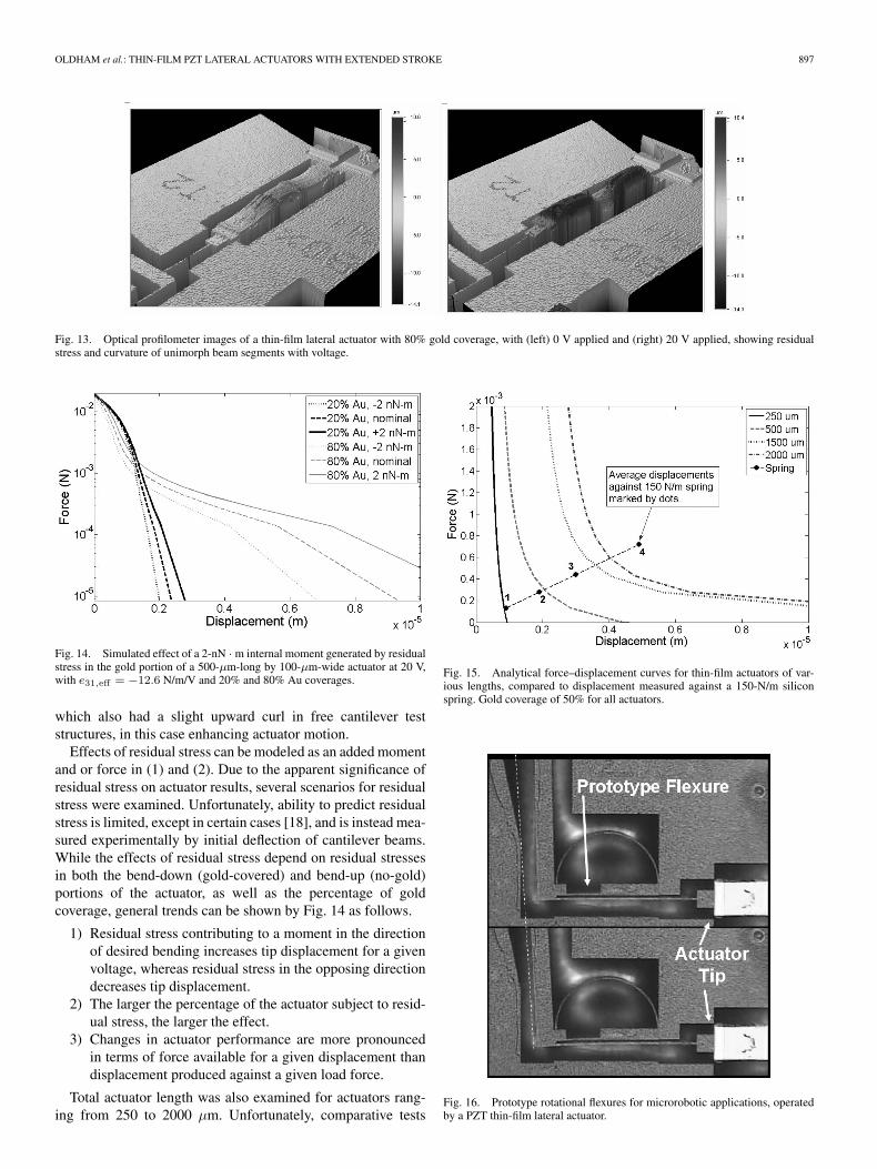
Fig. 13. Optical profilometer images of a thin-film lateral actuator with 80% gold coverage, with (left) 0 V applied and (right) 20 V applied, showing residualstress and curvature of unimorph beam segments with voltage.
Fig. 14. Simulated effect of a 2-nN · m internal moment generated by residualstress in the gold portion of a 500-µm-long by 100-µm-wide actuator at 20 V,with e31,eff = −12.6 N/m/V and 20% and 80% Au coverages.
which also had a slight upward curl in free cantilever teststructures, in this case enhancing actuator motion.
Effects of residual stress can be modeled as an added momentand or force in (1) and (2). Due to the apparent significance ofresidual stress on actuator results, several scenarios for residualstress were examined. Unfortunately, ability to predict residualstress is limited, except in certain cases [18], and is instead mea-sured experimentally by initial deflection of cantilever beams.While the effects of residual stress depend on residual stressesin both the bend-down (gold-covered) and bend-up (no-gold)portions of the actuator, as well as the percentage of goldcoverage, general trends can be shown by Fig. 14 as follows.
1) Residual stress contributing to a moment in the directionof desired bending increases tip displacement for a givenvoltage, whereas residual stress in the opposing directiondecreases tip displacement.
2) The larger the percentage of the actuator subject to resid-ual stress, the larger the effect.
3) Changes in actuator performance are more pronouncedin terms of force available for a given displacement thandisplacement produced against a given load force.
Total actuator length was also examined for actuators rang-ing from 250 to 2000 µm. Unfortunately, comparative tests
Fig. 15. Analytical force–displacement curves for thin-film actuators of var-ious lengths, compared to displacement measured against a 150-N/m siliconspring. Gold coverage of 50% for all actuators.
Fig. 16. Prototype rotational flexures for microrobotic applications, operatedby a PZT thin-film lateral actuator.

898 JOURNAL OF MICROELECTROMECHANICAL SYSTEMS, VOL. 17, NO. 4, AUGUST 2008
Fig. 17. Schematic top view of multiple (4) actuator arrays to generate (a) series rotational motion and (b) parallel translational motion.
typically varied by as much as a micrometer between mea-surements, because only test structures of spring type 1 wereincluded on the prototype wafers, and in the case of the longeractuators, optical profilometer resolution was limited by thelarge field of view required to test the actuators. Fig. 15 showsthe analytical force–displacement curves for actuators of fourdifferent lengths (250, 500, 1500, and 2000 µm) acting upon aspecific spring design for which three samples of each lengthcould be tested. Actuators of 1000 µm were also fabricatedbut were not released successfully. Measurement accuracy ofthe 1500- and 2000-µm actuators was only 1 µm, which isinsufficient to firmly establish agreement or disagreement be-tween the analytical model and actuator behavior, but the an-ticipated upward trend in actuator force and displacement wasobserved.
For many applications, multiple actuators are required toproduce desired displacements and/or forces. In these cases,the configuration of the actuators can have a significant effecton whether the excellent work capacity of the actuators alonemay be maintained. For instance, to generate the large rota-tional joint angles desired for microrobotic applications, severalactuators and flexures shown in Fig. 16 must be connectedin series, as shown schematically in Fig. 17(a). Sets of up tofour actuators have been tested experimentally, and designsincorporating eight or more flexures, which are capable of45◦ of motion and bearing significant out-of-plane loads, arecurrently under construction. In a configuration of this type, theconnections between actuators approximately double the arearequired to implement the actuators (not including the flexuralarea). On the other hand, when actuators are used in series orparallel for purely translational motion, actuators may be placedmuch more closely together, increasing effective area by onlyabout 25% [Fig. 17(b)]. Likewise, the tethers and flexures usedto maintain in-plane motion of the actuator tip when using asingle actuator also add to effective actuator area. A typicaltether has dimensions of 150 µm by 4 µm and, in the mostcompact form, is placed parallel with the flexure [as shown inFig. 17(a)] of about 100 µm by 8 µm. With an adjacent 30 µmof distance required on one side for etch holes, this increaseseffective actuator area by approximately 15% for a standard500-µm by 100-µm lateral actuator.
V. CONCLUSION
Thin-film piezoelectric actuators formed from compoundunimorph beams have demonstrated extremely high forceperformance in comparison to other MEMS actuation tech-nologies, with stroke lengths exceeding those of typicalpiezoelectric materials and maximum forces larger than othercommon microactuation technologies. Actuators were fabri-cated from chemical-solution-derived PZT thin films on asilicon-on-insulator wafer and were used to actuate a varietyof silicon test structures to evaluate force–displacement perfor-mance of a variety of actuator designs. These actuators havepotential to serve as an enabling technology for microroboticmanipulators and locomotion, among other applications. Futureresearch will focus on improving actuator robustness and thin-film properties while integrating the lateral actuators with alarger variety of microstructures.
REFERENCES
[1] W. C. Tang, T. C. H. Nguyen, M. W. Judy, and R. T. Howe, “Electrostatic-comb drive of lateral polysilicon resonators,” Sens. Actuators A, Phys.,vol. 21–23, pp. 328–331, Feb. 1990.
[2] T. Imamura, T. Koshikawa, and M. Katayama, “Transverse mode elec-trostatic microactuator for MEMS-based HDD slider,” in Proc. Int.Workshop MEMS, 1996, pp. 216–221.
[3] T. Akiyama and H. Fujita, “A quantitative analysis of scratch drive ac-tuator using buckling motion,” in Proc. IEEE Micro Electro Mech. Syst.,1995, pp. 310–313.
[4] R. B. Evans and J. S. Griesbach, “Piezoelectric microactuator for dual-stage control,” IEEE Trans. Magn., vol. 35, no. 2, pp. 977–982, Mar. 1999.
[5] N. J. Conway and S.-G. Kim, “Large-strain, piezoelectric, in-plane mi-croactuator,” in Proc. 17th IEEE Int. Conf. MEMS, 2004, pp. 454–457.
[6] J. S. Han, J. S. Ko, and J. G. Korvink, “Structural optimization of alarge-displacement electromagnetic Lorentz force microactuator for op-tical switching applications,” J. Micromech. Microeng., vol. 14, no. 11,pp. 1585–1596, Nov. 2004.
[7] W. Tang, V. Temesvary, R. Miller, A. Desai, Y.-C. Tai, and D. K. Miu,“Silicon micromachined electromagnetic microactuators for rigid diskdrives,” IEEE Trans. Magn., vol. 31, no. 6, pp. 2964–2966, Nov. 1995.
[8] M. J. Sinclair, “A high force low area MEMS thermal actuator,” in Proc.7th Intersoc. Conf. Therm. Thermomech. Phenom. Electron. Syst., 2000,pp. 127–132.
[9] C. H. Pan, C.-L. Chang, and Y.-K. Chen, “Design and fabricationof an electro-thermal microactuator with multidirectional in-plane mo-tion,” J. Microlithogr. Microfabr. Microsyst., vol. 4, no. 3, pp. 1–15,Jul. 2005.
[10] Y. Haddab, N. Chaillet, and A. Bourjalt, “A microgripper using smartpiezoelectric actuators,” in Proc. Intell. Robots Syst., 2000, pp. 659–664.

OLDHAM et al.: THIN-FILM PZT LATERAL ACTUATORS WITH EXTENDED STROKE 899
[11] R. G. Polcawich, J. S. Pulskamp, D. Judy, P. Ranade, S. Trolier-McKinstry, and M. Dubey, “Surface micromachined microelectro-mechanical ohmic series switch using thin-film piezoelectric actuators,”IEEE Trans. Microw. Theory Tech., vol. 55, no. 12, pp. 2642–2654,Dec. 2007.
[12] K. Oldham, J. S. Pulskamp, R. Polcawich, and M. Dubey, “Thin-filmpiezoelectric microactuators for bio-inspired micro-robotic applications,”presented at the Int. Symp. Integrated Ferroelectrics, Bordeaux, France,2007.
[13] P. Muralt, A. Kholkin, M. Kohli, and T. Maeder, “Piezoelectric actuationof PZT thin-film diaphragms at static and resonant conditions,” Sens.Actuators A, Phys., vol. 53, no. 1, pp. 398–404, May 1996.
[14] D. A. Hall, “Review: Nonlinearity in piezoelectric ceramics,” J. Mater.Sci., vol. 36, no. 19, pp. 4575–4601, Oct. 2001.
[15] K. Budd, S. Dey, and D. Payne, “Sol-gel processing of PbTiO3,PbZrO3, PZT, and PLZT thin films,” Proc. Brit. Ceramics Soc., vol. 36,pp. 107–121, 1985.
[16] W. N. Sharpe, J. Pulskamp, D. S. Gianoia, C. Eberi, R. G. Polcawich, andR. J. Thompson, “Strain measurements of silicon dioxide microspecimensby digital imaging processing,” Exp. Mech., vol. 47, no. 5, pp. 649–658,Oct. 2007.
[17] K. J. Hemker and W. N. Sharpe, Jr., “Microscale characterization ofmechanical properties,” Annu. Rev. Mater. Res., vol. 37, pp. 93–126,Feb. 2007.
[18] J. S. Pulskamp, A. Wickenden, R. Polcawich, B. Piekarski, M. Dubey,and G. Smith, “Mitigation of residual film stress deformation in multilayermicroelectromechanical systems cantilever devices,” J. Vac. Sci. Technol.B, Microelectron. Process. Phenom., vol. 21, no. 6, pp. 2482–2486,Nov. 2003.
Kenn R. Oldham received the B.S. degree in me-chanical engineering from Carnegie Mellon Univer-sity, Pittsburgh, PA, in 2000, and the Ph.D. degreein mechanical engineering from the University ofCalifornia, Berkeley, in 2006.
He is currently an Assistant Professor with theDepartment of Mechanical Engineering, Universityof Michigan, Ann Arbor. His research interests in-clude microactuation design and application, optimaldesign and control, and efficient sensing and powercircuitry for MEMS devices.
Prof. Oldham is a member of the American Society of Mechanical Engineers.
Jeffrey S. Pulskamp received the B.S. degreein mechanical engineering from the University ofMaryland, College Park, in 2000.
He is currently a Mechanical Engineer with theMicro and Nano Electronic Materials and DevicesBranch, U.S. Army Research Laboratory, AdelphiLaboratory Center, Adelphi, MD. His current re-search interests include RF MEMS devices, elec-tronic scanning antennas, mechanical modeling ofMEMS, MEMS actuator design, and millimeter-scale robotics.
Ronald G. Polcawich (M’07) received the B.S.degree in materials science and engineering fromCarnegie Mellon University, Pittsburgh, PA, in 1997,and the M.S. (in 1999) and Ph.D. degrees inmaterials from The Pennsylvania State University,University Park.
He is currently an Engineer and a Team Lead forthe RF MEMS Group, Micro and Nano ElectronicMaterials and Devices Branch, U.S. Army ResearchLaboratory, Adelphi Laboratory Center, Adelphi,MD. His research interests include RF MEMS de-
vices, electronic scanning antennas, PZT thin films, MEMS fabrication, MEMSactuators, and millimeter-scale robotics.
Dr. Polcawich is a member of the Materials Research Society.
Madan Dubey received the Ph.D. degree in physicsfrom Banaras Hindu University, Varanasi, India,in 1977.
He is currently a Research Physical Scientist withthe Advanced Micro Devices Branch, U.S. ArmyResearch Laboratory, Adelphi Laboratory Center,Adelphi, MD. He is leading a team of researchersin the area of nanoelectronics. He was a Postdoc-toral Fellow with North Carolina State University,Raleigh, and was also a Research Engineer withthe Research Triangle Institute, Research Triangle
Park, NC.