tianmu xin - graduate physics and astronomy at...
TRANSCRIPT

Electron Source based on Superconducting RF
A Dissertation Presented
by
Tianmu Xin
to
The Graduate School
in Partial Fulfillment of the
Requirements
for the Degree of
Doctor of Philosophy
in
Physics
Stony Brook University
May 2016

ii
Stony Brook University
The Graduate School
Tianmu Xin
We, the dissertation committee for the above candidate for the
Doctor of Philosophy degree, hereby recommend
acceptance of this dissertation.
Prof. Ilan Ben-Zvi, Brookhaven National Lab– Dissertation Advisor
Prof. Jacobus Verbaarschot, Department of Physics and Astronomy - Chairperson of Defense Prof. Maria Victoria Fernandez-Serra, Department of Physics and Astronomy
Dr. Qiong Wu, Brookhaven National Lab
This dissertation is accepted by the Graduate School
Charles Taber Dean of the Graduate School

iii
Abstract of the Dissertation
Electron Source based on Superconducting RF
by
Tianmu Xin
Doctor of Philosophy
in
Physics
Stony Brook University
2016
High-bunch-charge photoemission electron-sources operating in a Continuous Wave (CW) mode can provide high peak current as well as the high average current which are required for many advanced applications of accelerators facilities, for example, electron coolers for hadron beams, electron-ion colliders, and Free-Electron Lasers (FELs).
Superconducting Radio Frequency (SRF) has many advantages over other electron-injector technologies, especially when it is working in CW mode as it offers higher repetition rate. An 112 MHz SRF electron photo-injector (gun) was developed at Brookhaven National Laboratory (BNL) to produce high-brightness and high-bunch-charge bunches for electron cooling experiments. The gun utilizes a Quarter-Wave Resonator (QWR) geometry for a compact structure and improved electron beam dynamics. The detailed RF design of the cavity, fundamental coupler and cathode stalk are presented in this work. A GPU accelerated code was written to improve the speed of simulation of multipacting, an important hurdle the SRF structure has to overcome in various locations.
The injector utilizes high Quantum Efficiency (QE) multi-alkali photocathodes (K2CsSb) for generating electrons. The cathode fabrication system and procedure are also included in the thesis.
Beam dynamic simulation of the injector was done with the code ASTRA. To find the optimized parameters of the cavities and beam optics, the author wrote a genetic algorithm Python script to search for the best solution in this high-dimensional parameter space.
The gun was successfully commissioned and produced world record bunch charge and average current in an SRF photo-injector.

iv
Table of Contents
Introduction ..................................................................................................................................... 1
1 The Design and Fabrication of the 112 MHz QWR SRF Cavity ........................................... 4
1.1 Cavity Design ................................................................................................................... 4
1.1.1 The frequency of the RF Resonator. ......................................................................... 5
1.1.2 The quality factor of an RF cavity .......................................................................... 12
1.1.3 The Shunt Impedance and R/Q ............................................................................... 13
1.1.4 The Transit Time Factor and the Acceleration Voltage .......................................... 13
1.1.5 The Peak Surface Field ratios and .......................................................... 15
1.2 Multipacting Study ......................................................................................................... 16
1.2.1 Multipacting ............................................................................................................ 16
1.2.2 Examples of Multipacting ....................................................................................... 18
1.2.3 Analytical treatment of multipacting ...................................................................... 19
1.2.4 Method of simulation .............................................................................................. 22
1.2.5 GPU code for multipacting simulation and results ................................................. 22
1.3 Tuning: Simulation and Measurements.......................................................................... 28
1.4 Summary ........................................................................................................................ 34
2 Fundamental Power Coupler (FPC) / Fine Tuner Design and Fabrication ........................... 35
2.1 RF Design of the FPC .................................................................................................... 35
2.2 Thermal Analysis ........................................................................................................... 38
2.3 Multipacting Study ......................................................................................................... 40
2.4 Summary ........................................................................................................................ 41
3 Cathode and Insertion System .............................................................................................. 42

v
3.1 Cathode Stalk Design ..................................................................................................... 42
3.2 Cathode Preparation ....................................................................................................... 46
3.3 The Cathode Insertion System ....................................................................................... 48
3.4 Multipacting Study ......................................................................................................... 49
3.5 Summary ........................................................................................................................ 50
4 Beam Dynamics Simulation ................................................................................................. 51
4.1 Emittance of a Beam ...................................................................................................... 51
4.2 Beam Simulation ............................................................................................................ 60
4.3 Summary ........................................................................................................................ 64
5 112MHz SRF Electron Injector Commissioning .................................................................. 65
5.1 SRF Commissioning ...................................................................................................... 65
5.2 Photocurrent Measurement ............................................................................................ 68
5.3 Summary ........................................................................................................................ 72
6 Alternative Cathode for the Gun: Diamond Amplifier ......................................................... 73
6.1 Diamond as Secondary Electron Emitter ....................................................................... 73
6.2 Diamond Amplifier for 112 MHz SRF Injector ............................................................. 74
6.3 Summary ........................................................................................................................ 80
7 Conclusion ............................................................................................................................ 81
References: .................................................................................................................................... 83
vi
List of Figures
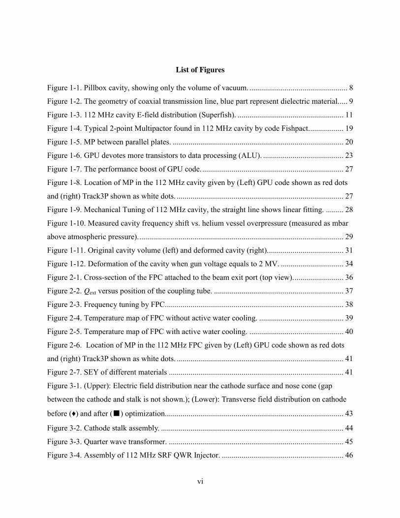
Figure 1-1. Pillbox cavity, showing only the volume of vacuum. .................................................. 8
Figure 1-2. The geometry of coaxial transmission line, blue part represent dielectric material..... 9
Figure 1-3. 112 MHz cavity E-field distribution (Superfish). ...................................................... 11
Figure 1-4. Typical 2-point Multipactor found in 112 MHz cavity by code Fishpact. ................. 19
Figure 1-5. MP between parallel plates. ....................................................................................... 20
Figure 1-6. GPU devotes more transistors to data processing (ALU). ......................................... 23
Figure 1-7. The performance boost of GPU code. ........................................................................ 27
Figure 1-8. Location of MP in the 112 MHz cavity given by (Left) GPU code shown as red dots
and (right) Track3P shown as white dots. ..................................................................................... 27
Figure 1-9. Mechanical Tuning of 112 MHz cavity, the straight line shows linear fitting. ......... 28
Figure 1-10. Measured cavity frequency shift vs. helium vessel overpressure (measured as mbar
above atmospheric pressure). ........................................................................................................ 29
Figure 1-11. Original cavity volume (left) and deformed cavity (right). ...................................... 31
Figure 1-12. Deformation of the cavity when gun voltage equals to 2 MV. ................................ 34
Figure 2-1. Cross-section of the FPC attached to the beam exit port (top view). ......................... 36
Figure 2-2. Qext versus position of the coupling tube. .................................................................. 37
Figure 2-3. Frequency tuning by FPC........................................................................................... 38
Figure 2-4. Temperature map of FPC without active water cooling. ........................................... 39
Figure 2-5. Temperature map of FPC with active water cooling. ................................................ 40
Figure 2-6. Location of MP in the 112 MHz FPC given by (Left) GPU code shown as red dots
and (right) Track3P shown as white dots. ..................................................................................... 41
Figure 2-7. SEY of different materials ......................................................................................... 41
Figure 3-1. (Upper): Electric field distribution near the cathode surface and nose cone (gap
between the cathode and stalk is not shown.);; (Lower): Transverse field distribution on cathode
before (♦) and after () optimization. .......................................................................................... 43
Figure 3-2. Cathode stalk assembly. ............................................................................................. 44
Figure 3-3. Quarter wave transformer. ......................................................................................... 45
Figure 3-4. Assembly of 112 MHz SRF QWR Injector. .............................................................. 46

vii
Figure 3-5. Multi-alkali deposition system for the 112 MHz gun. ............................................... 47
Figure 3-6. Photograph of polished molybdenum pucks before deposition of the photoemission
layer............................................................................................................................................... 47
Figure 3-7. Cross-sectional view of the cathode insertion system................................................ 48
Figure 3-8. Cathode end assembly. ............................................................................................... 49
Figure 3-9. Multipactors between the cathode stalk and the cavity. The MP appears at around
600 kV gun voltage. ...................................................................................................................... 49
Figure 3-10. Enhanced counter function of MP in cathode stalk with copper surface, gold plating
and TiN coating............................................................................................................................. 50
Figure 4-1. Three-step model for the metal cathode. .................................................................... 53
Figure 4-2. Schematic layout of 112 MHz injector. ..................................................................... 60
Figure 4-3. Transverse emittance vs. distance from cathode. ....................................................... 63
Figure 4-4. Time profile of bunch at the exit of LINAC. ............................................................. 63
Figure 4-5. RMS energy spread vs. distance from the cathode. ................................................... 64
Figure 5-1. The layout of 112 MHz SRF injector (low energy experiment). ............................... 65
Figure 5-2. Quality factor measurement of the cavity without cathode stalk and FPC. ............... 66
Figure 5-3. 𝑄 measured after the installation of FPC and cathode stalk. .................................... 66
Figure 5-4. Image of field emitter from the cavity. ...................................................................... 67
Figure 5-5. Upper plot shows the gun voltage near the end of helium processing, lower plot
shows the radiation does decrease. ............................................................................................... 68
Figure 5-6. The laser path (bright green lines) and details of FPC and cathode in 112 MHz
injector . ........................................................................................................................................ 69
Figure 5-7. Measured charge dependency on laser energy under 1.56 MV gun voltage . ........... 70
Figure 5-8. Raw and integrated ICT signal. The ICT calibration is 0.8 nC per 1 nV. The signal
here corresponding to a 2.4 nC bunch charge . ............................................................................. 71
Figure 5-9. Vertical shift of beam position at YAG 1 versus current in Trim D . ........................ 72
Figure 6-1. Schematic diagram of the diamond amplifier . .......................................................... 74
Figure 6-2. Section view of the Diamond Amplifier: red lines show the path of UV light. Small
insert is a photo of the first prototype Amplifier with a penny on the side as a size reference. ... 75
Figure 6-3. Laser path (red) and electron path (green) in the Amplifier and cavity. .................... 76

viii
Figure 6-4. Trajectory of electron beam between the primary cathode and diamond. Smaller
picture shows the potential distribution inside the Amplifier. ...................................................... 77
Figure 6-5. Demonstration of the laser beam passage. ................................................................. 78
Figure 6-6. Percentage of electrons reaching dummy electrode over electrons leaving cathode. 79
Figure 6-7. (a) Mask used for lithography; (b) Picture of back electrode made with patterned
mask. The grid spacing is 50 µμm . ................................................................................................ 80

ix
List of Tables
Table 1-1. Design parameters of 112 MHz cavity. ....................................................................... 15
Table 2-1. Parameters of the fundamental power coupler ............................................................ 35
Table 2-2. Emissivity of copper and gold ..................................................................................... 40
Table 3-1. Comparison of RF losses on a uniform stalk and a stalk with an impedance
transforming step at an accelerating voltage of 2 MV. ................................................................. 46
Table 4-1. Parameter ranges for 112 MHz injector ...................................................................... 60
Table 4-2. Objectives of optimization of 112 MHz injector ......................................................... 61
Table 6-1. Parameters for simulation ............................................................................................ 76
x
Acknowledgments
I received support from many during the course of this work, and I’d like to show my
gratitude to all that generously gave the time to answer my question, provide ingenious
inspiration and sometime rescue me from the inevitable setbacks in the experiment.
On top of the list is my advisor Professor Ilan Ben-Zvi for his support, supervision, advice
and guidance from the very early stage of my accelerator career. I am honored to become
one of his students and would like to convey my deepest respect to him through this
humble acknowledgment. His passion and diligence in research work inspired me and will
benefit me in the future. He is the most encouraging and supportive advisor I could ever
ask for. None of the work I presented in this thesis could have been done without his
backup.
Professor Sergey Belomestnykh as my group leader in SRF group gave me countless great
suggestions in my research work. He was always willing to help me solve whatever
problem I encountered in my work and, most impressively, with ease for almost all the
headache giving puzzles I threw at him.
Since my very first day at Brookhaven National Lab, Dr. Qiong Wu taught me all the
hands-on skills that proved to be priceless in my daily research. I can never thank her
enough for her patience and teaching skill when I was completely new in the SRF and
Diamond Amplifier field. I would like to say the same to Dr. Xiangyun Chang for leading
me into the Diamond Amplifier program and teaching me experimental skills and inspiring
me with his ingenious ideas when dealing with new problems.
I am also very grateful to Dr. Jörg Kewisch for the productive discussions we had on the
GPU simulation and genetic algorithm optimizer project.
I would like to give my special thanks to the cathode group, Erdong Wang, Triveni Rao,
John Skaritka, John Walsh, and William Smith. They taught me much knowledge that a
qualified experimentalist should have, with patience and kindness. It is my honor to work
with such a great team and learn from them.

xi
I would also like to show my gratitude to the CEC group and all the people that work so
hard for this project, Vladimir Litvinenko, Igor Pinayev, Joseph Tuozzolo, Jean Clifford
Brutus, Yue Hao, James Jamilkowski, Yichao Jing, Dmitry Kayran, George Mahler,
Michael Mapes, Toby Miller, Geetha Narayan, Brian Sheehy, Kevin Smith, Yatming Than,
Gang Wang, Binping Xiao, Alexander Zaltsman, Wuzheng Meng, Wencan Xu, Yuan Hui
Wu, Zhi Zhao. None of the work could be done without the contributions from every one of
you.
I also wish to thank Professor Jacobus Verbaarschot and Professor Marivi Fernandez-Serra
for serving on my thesis committee and taking time to review my thesis. Their great
suggestions and comments are invaluable to this thesis.
Finally, I would like to end this acknowledgment with my sincere appreciation to my
family. Their support and understanding are what led me to this distinct point in my life.
Special thanks are due to my wife for going through so much hardship with me over all
these years.

1
Introduction The high peak and average current electron injector with good emittance is of great
importance in the next generation light source (FEL driven) [1], high-energy electron
coolers [2, 3], and essentially all the facilities that require high brightness and high
average power electron beams.
In this work we present the design, building and commissioning of a Superconducting
Radio Frequency (SRF) electron injector with a high Quantum Efficiency (QE) multi-
alkali photocathode [4] that is capable of providing electron beams with better than 7.5
mm-mrad transverse emittance, energy spread smaller than 5x10⁻³ and bunch charge as
large as 3 nC. The injector consists of several critical parts including the 112 MHz SRF
cavity, the coaxial type Fundamental Power Coupler (FPC), the half wavelength choke
structure cathode stalk with cathode insertion system and high quantum efficiency multi-
alkali photocathode.
The 112 MHz quarter wave resonator cavity was designed, built and tested in previous
work [5]. We took it as the base of the new injector for the Coherent Electron Cooling
(CeC PoP) experiment. Although the major part of RF design of the cavity has been done
years before the design of this injector [6], there were still critical items to be designed
and resolved. As examples we can mention the multipacting (MP) study, Lorentz
detuning, mechanical tuning sensitivity and detuning due to helium pressure change.
Furthermore, there were essential subsystems of the injector to be designed, constructed
and commissioned, such as the Fundamental Power Coupler (FPC), the coarse tuner and
the photocathode insertion system. All these elements are critical for making the cavity
usable as an injector, and will be discussed in more details later.
The coaxial type of Fundamental Power Coupler (FPC) is designed to provide up to 780-
W power to the electron bunches [7]. Besides the main role of a power coupler the FPC
can also be used as a fine tuner of the injector to adjust the frequency more precisely
compare to the mechanical tuner. With the help of the commercial computer simulation
codes CST and ANSYS, the author performed the RF simulation and thermal analysis of
the FPC. The multipacting issue of the FPC was a major concern when we were

2
considering the coaxial structure. Both GPU code, which was developed by the author for
the MP simulation and the ACE3P [8] code were used. Simulation results provided
information on the RF voltage levels, locations and strength of the multipacting, and
suggested the possibility of easing the problem with gold coating, which has a lower
secondary electron yield as compared to pure copper. Moreover, the gold coating
provides smaller emissivity, 50% better than copper and the forty times better than the
oxidized copper which means proportionally less radiation thermal load to the
cryosystem.
In order to simplify the photocathode insertion system, we had to find a way to insert the
cathode into the cavity, which is at 4.5 K, without cooling the cathode to the same
temperature. In addition, according to recent work done by E. Wang and H. Xie at BNL,
the quantum efficiency of K2CsSb cathode at 532 nm will drop substantially at cryogenic
temperatures [9], adding to the incentive of keeping the cathode warm. A choke-joint
structure is a natural choice for the implementation of this design, thanks to its capability
to provide an electrical short at the cavity side of the insert and yet to provide thermal
isolation [10]. A half wavelength choke-joint cathode stalk was designed to hold the
cathode in the desired position inside the cavity. Impedance mismatch was implemented
to further reduce the impedance of the stalk seen by the cavity. The thermal and
multipacting issues in the cathode insertion system were also investigated intensively, as
in the FPC case. The gold coating solved the problems according to the simulation, and
the details are discussed in Chapter 4. The heart of the injector, where everything starts
from, is the cathode. The performance of the cathode sets the ultimate quality of the beam
downstream. We decided to use the multi-alkali (K2CsSb) photocathode for its high
quantum efficiency under green light and acceptable vacuum tolerance. The recipe of
fabricating K2CsSb has been well developed [11], and we adopted it with some
modifications aimed at improving its performance in our system.
To investigate the multipacting phenomenon in the SRF structure, the author developed a
3D particle tracking code with C language, which utilizes Graphic Processor Unit (GPU)
acceleration. The code tracks the electrons in tetrahedral mesh elements under the pre-
calculated electromagnetic (EM) field. The unique feature of the code is that it takes

3
advantage of the high concurrency of the GPU and updates coordinates of thousands of
particle in 6-D phase space (three spatial plus three momentum) simultaneously. By
parallelizing the most time-consuming parts of the algorithm the execution time of the
GPU version of the code can be five times faster than the CPU version on a Nvidia Tesla
K40. A detailed discussion can be found in Chapter 2.
Another important element of the design and commissioning of the injector is the beam
dynamics simulation. Since this is a multi-parameter multi-objective optimization
problem, the author decided to solve it by using a genetic algorithm. A python script was
written to search for the combination of operating parameters that meets the requirement
of the experiment. Simulation results given by ASTRA [12] show that the injector is
capable of generating 2 nC/bunch beam with better than 7.5 mm-mrad transverse
emittance and 0.5% energy spread.
A special type of cathode, Diamond Amplifier, is discussed in Chapter 7 of the thesis. We
designed the housing components of the amplifier integrated with the primary cathode
holder [13]. The laser optics and electron transport of the primary electron beam were
tested in a chamber independent of the SRF injector. The result of the preliminary test is
promising. If we have the opportunity to test the amplifier in an SRF injector in future,
we should be able to demonstrate the great potential of the diamond amplifier in high
peak/average current injector.
The electron injector driven by 112 MHz QWR SRF cavity and K2CsSb cathode has been
tested for the first time at BNL during the RHIC run 15, namely from the December 2014
to June 2015. We were able to extract a world record bunch charge and average current
for a superconducting electron gun to date. The injector delivered up to 3 nC/bunch
electron with a repetition rate as high as 5 kHz (limited by laser system at the time),
leading to an average current of 15 µμA.
4
1 The Design and Fabrication of the 112 MHz QWR SRF Cavity
1.1 Cavity Design A careful design of the electron gun is the key to the good performance of any electron
accelerator. The electron bunch leaves the surface of the cathode and gains the initial
energy boost within this device. The critical issue that requires careful consideration is
the form of the electromagnetic field regarding both the time and spatial structure. The
simplest choice is to use the DC Pierce shape electrode [14]. However, the DC approach
is limited by surface field strength which consequently limits the current density one can
extract from the cathode. Furthermore, to minimize emittance growth, a rapid
acceleration of the electrons is necessary. Therefore, we chose to use an RF cavity instead.
Furthermore, to get a CW operating beam we decided to use a superconducting quarter
wave cavity operating at 112 MHz frequency. The 112 MHz quarter wave resonator
(QWR) cavity was mainly designed in previous work of Xiangyun Chang. For the sake of
completeness of the story, we will briefly recapitulate the work and considerations during
the design of cavity.
To get a high bunch charge and maintain a good emittance, one needs to mitigate the
space charge limitation which means using a high electric field on the cathode surface.
The typical surface gradient that a DC structure can provide is in the range of 5 to 10-
MV/m [15], which is limited by the discharging phenomenon from the field emission tips
on the electrode. However, an RF structure can easily provide a much higher field
gradient on the cathode surface. For a superconducting cavity the field strength can be
around 20 to 30 MV/m [16, 17] and for a pulsed normal conducting cavity the field level
can be even as high as 100 MV/m [18]. The disadvantage of a normal conducting cavity,
typically made of high purity copper, is that this kind of cavity can only run at a relatively
low duty factor, which will have a large negative impact on the average current.
Considering the injector’s frequency, reducing the peak current density also helps in
getting a higher bunch charge. The 112 MHz cavity has a much lower frequency than a
traditional SRF cavity ( for example the Tesla 1.3 GHz cavity [19]) which means the
bunch length (typically in the order of 10 degrees of the RF cycle) can be much longer,
hence reduce the current density linearly. For a cavity with such a low frequency, the

5
elliptical shape cavity is no longer the optimum choice due to its large diameter, and this
is the reason we chose quarter wave resonator instead.
To increase the average current once the bunch charge is limited by the achievable
strength of the surface field, the most straightforward way is to increase the repetition
rate of the bunch. That is best done by delivering the beam in a Continuous Wave (CW)
mode, which means that ultimately each RF cycle can support one bunch so that the
average current of the beam can be maximized. As we mentioned before, the traditional
normal conducting cavity at a high RF field can only work under pulsed mode with a
duty factor low enough so that the thermal load to the structure and peripheral devices
can be handled. Hence, the normal conducting cavity, with very few exemptions [20],
cannot provide a CW beam. This is where the superconducting cavity shines since it
generates as much as six orders of magnitude lower RF power dissipation compared to a
normal conducting cavity at the same frequency [17]. This makes it clear that the SRF
cavity is a very strong candidate for high bunch charge high average current electron
injector.
Taking all the factors into account, we eventually decided to use the 112 MHz QWR SRF
cavity as the electric field generating cavity of the injector.
Here we briefly introduce the key parameters of an SRF cavity, namely the frequency,
quality factor, geometry factor, R/Q, Bmax/Eacc, Emax/Eacc, and transit time factor.
1.1.1 The frequency of the RF Resonator. One of the most common RF cavity people use as a model is the so-called pillbox cavity
model [21]. The typical shape of the cavity is shown in Figure 1-1. The equation of the
EM field in such a structure can be written as the following.
Starting from the basic Maxwell’s equations
∇ ∙ 𝐸 =𝜌𝜖,
∇ × 𝐸 = −𝜕𝐵𝜕𝑡
,
∇ ∙ 𝐵 = 0,
( 1-1 )

6
∇ × 𝐵 = 𝜇 𝐽 +1𝑐𝜕𝐸𝜕𝑡,
where 𝜌 is the charge density in unit of C/m3, 𝜖 is the vacuum permittivity equal to
8.854 × 10 F/m in SI unit, 𝜇 is the vacuum permeability equals to 4𝜋 × 10 H/m
in SI unit and 𝐽 is the current density in unit of A/m2.
Consider the free space case and take the curl of the second equation above,
∇ × (∇ × 𝐸) = ∇ × (∇ ∙ 𝐸) − ∇ 𝐸 = −𝜕𝜕𝑡(∇ × 𝐵),
∇ 𝐸 −1𝑐𝜕𝐸𝜕𝑡
= 0.
Similarly for the magnetic part,
∇ 𝐵 −1𝑐𝜕𝐵𝜕𝑡
= 0.
Now we got the famous EM wave equations. Assuming the harmonic time dependence of
EM field 𝑒 , where 𝜔 is the angular frequency of the oscillation, we can get
(∇ +
𝜔𝑐)
𝐸𝐵
= 0, ( 1-2 )
where c is the speed of light in vacuum.
In a cylindrical geometry, following the approach Jackson chose in his book [22] we can
separate the transverse and longitudinal parts of the fields as the following,
𝐸 = 𝐸(𝑥, 𝑦)𝑒± ,
𝐵 = 𝐵(𝑥, 𝑦)𝑒± , ( 1-3 )
with 𝑘 representing the wave number defined as 𝑘 = , where 𝜆 is the wave length of
the EF field.
Hence, we can write the wave equation as

7
(∇ +
𝜔𝑐
− 𝑘 ) 𝐸𝐵
= 0, ( 1-4 )
where ∇ = ∇ − , if we further decompose the field into transverse and longitudinal
components in explicit way we will get,
= + ; 𝐵 = 𝐵 + 𝐵 .
Substituing this form of field into the equation ( 1-1 ) we can get the relation between the
transverse and the longitudinal field as
𝐸 =𝑖
𝜔𝑐 − 𝑘
[𝑘∇ 𝐸 − 𝜔 × ∇ 𝐵 ],
𝐵 =𝑖
𝜔𝑐 − 𝑘
𝑘∇ 𝐵 +𝜔𝑐 × ∇ 𝐸 ,
( 1-5 )
where is the unit vector in z direction.
For the TM mode, which is the common accelerating mode, we have 𝐵 = 0 everywhere.
Hence,
𝐸 =𝑖
𝜔𝑐 − 𝑘
[𝑘∇ 𝐸 ],
𝐵 =𝑖
𝜔𝑐 − 𝑘
𝜔𝑐 × ∇ 𝐸 .
( 1-6 )
In a pillbox cavity, we can write the longitudinal electric field as
𝐸 = 𝜓(𝑟)𝑒± , ( 1-7 )
with 𝑘 = 𝑝 , 𝑝 = 0,1,2,3… , 𝜙 as the azimuthal angle in cylindrical coordinate, and d is
the length of the pillbox cavity in z direction.
Then from equation ( 1-6 ) we can get the new equation for the r dependent part of 𝐸 as

8
1𝑟𝑑𝑑𝑟
𝑟𝑑𝑑𝑟
−𝑚𝑟
+ 𝛾 𝜓 = 0. ( 1-8 )
In a cylindrical coordinate with boundary condition 𝜓(𝑟 = 𝑎) = 0 we have the following
solutions
𝜓 = 𝐸 𝐽 (𝜅𝑟), ( 1-9 )
where 𝐽 is mth order Bessel function. For the fundamental mode we have
𝜔 = 𝑐𝜅 =𝑐𝑗 ,
𝑎=2.4048 𝑐
𝑎, ( 1-10 )
where 𝑗 , is the first zero point of zeroth order Bessel function which is 2.4048 and 𝑎 is
the radius of the pillbox cavity.
Figure 1-1. Pillbox cavity, showing only the volume of vacuum.
As we can see, the fundamental mode frequency of the pillbox type cavity is directly
related to the transverse size of the cavity. If we would like to build a cavity which works
at a frequency 𝑓 = 100 MHz, the radius of the cavity would be in the order of 1.15 m
which could be quite difficult to handle. Hence we need the so-called TEM mode cavity
when looking into the low frequency application [23]. One cavity of this type is the
quarter wave resonator (QWR) cavity [24, 25].

9
For a QWR cavity, the boundary condition is different. It is more closely related to the
coaxial transmission line model. The geometry of a coaxial transmission line can be
generalized as shown in Figure 1-2. The scalar potential 𝜙(𝑟, 𝜃) between the inner and
outer conductor satisfies the following equation.[26]
1𝑟𝜕𝜕𝑟
𝑟𝜕𝜙𝜕𝑟
+1𝑟𝜕 𝜙𝜕𝜃
= 0, ( 1-11 )
Figure 1-2. The geometry of coaxial transmission line, blue part represent dielectric
material.
Now we can separate the variables, 𝜙 = 𝑅(𝑟)𝑇(𝜃) and substitute back into equation
( 1-11 ) and dividing both side by RT we get
𝑟𝑅𝜕𝜕𝑟
𝑟𝑑𝑅𝑑𝑟
+1𝑇𝑑 𝑇𝑑𝜃
= 0. ( 1-12 )
Two of the terms above must be constants, therefore we set:
a b
y
x
z r
𝜃

10
𝑟𝑅𝜕𝜕𝑟
𝑟𝑑𝑅𝑑𝑟
= −𝑘 ,
1𝑇𝑑 𝑇𝑑𝜃
= −𝑘 . ( 1-13 )
For the TEM mode, the boundary condition does not change with respect to 𝜃, hence
𝑘 = 0, consequently 𝑘 = 0. This gives us
𝜕𝜕𝑟
𝑟𝑑𝑅𝑑𝑟
= 0. ( 1-14 )
The solution of equation ( 1-14 ) is then:
𝑅 = 𝐴 ln𝑟 + 𝐵, 𝑎 < 𝑟 < 𝑏. ( 1-15 )
This is the scalar potential of the transverse field with constants A and B determined by
boundary conditions.
Now assume one end (z=0) of the transmission line is shorted, and the other end (z=d) is
open. Namely, the boundary conditions on z=0 and z=d require that 𝐸 (𝑧 = 0) = 0,
𝐻 (𝑧 = 𝑑) = 0 respectively. Hence the z dependence of the E field of TEM mode turns
out to be
𝐸 = 𝐸 (𝑟) sin 𝑘𝜋𝑑𝑧 , 𝑘 =
12,32,…
This is the stationary waveform of the field, and the frequency of the lowest order mode
is
𝜔 = 𝑐𝜋2𝑑
.
In other words, the wave number of lowest mode is
𝜆 = 4𝑑,
where d is the length of the cavity hence the name of quarter wave resonator.
Besides its compact size, one of the advantages of the QWR cavity is the large separation
between the fundamental mode and next higher order TEM mode [27]. From the

11
boundary conditions, we can easily see that the frequency of next higher order mode is
about three times of the fundamental mode where k = 3/2 instead of 1/2. This is important
when the cavity is used with high beam currents, where higher order mode (HOM)
damping is a more critical issue and larger mode separation between the fundamental
mode and next high order mode will make the design of HOM filter easier.
A more realistic QWR is shown Figure 1-3. This is the Superfish [28] plot of our 112
MHz cavity. We can see the length of the cavity is 86.57 cm, which is slightly larger than
¼ of the wavelength of 112 MHz TEM mode in an ideal QWR. The reason for this
difference is that we need to introduce a gap to provide space for the acceleration of the
beam. Various other modifications have been made to the cavity to make it suitable for an
electron injector. The shape of the inner conductor is altered to reduce the peak surface
magnetic field. The nose cone part, which is the tip of the end of the inner conductor, has
been rounded to reduce the peak surface electric field [29]. The cathode stalk, which can
be partially seen from the picture, has to be designed such that we can insert the cathode
into the cavity without compromising the thermal insulation between the cryo-
environment of cavity and cathode system [7].
Figure 1-3. 112 MHz cavity E-field distribution (Superfish).

12
1.1.2 The quality factor of an RF cavity Another critical figure of merit of an RF cavity is the quality factor. The definition of the
quality factor of the cavity is
𝑄 = 𝜔𝑈𝑃, ( 1-16 )
where 𝜔 is the frequency of the interested mode, U is the energy stored in the cavity, 𝑃
is the RF power dissipation on cavity wall. The physical meaning of 𝑄 is how many RF
angular cycles does it take for the cavity to lose the stored energy due to the wall power
dissipation.
As we know from general EM theory, the stored energy of EM field in cavity is
𝑈 =12𝜇 |𝐻| 𝑑𝑉. ( 1-17 )
For the power dissipated on cavity wall we have
𝑃 =
12𝑅 |𝐻| 𝑑𝑠, ( 1-18 )
where 𝑅 is the surface resistance of the cavity wall material and we are assuming same
𝑅 everywhere here.
Therefore, the quality factor can also be written as
𝑄 = 𝜔
𝜇 ∮ |𝐻| 𝑑𝑉
𝑅 ∮ |𝐻| 𝑑𝑆=
𝐺𝑅, ( 1-19 )
where
𝐺 =
𝜔𝜇 ∮ |𝐻| 𝑑𝑉
∮ |𝐻| 𝑑𝑆, ( 1-20 )
is the so-called geometry factor of the cavity. For a given mode, the geometry factor
depends only on the shape of the cavity. The typical geometry factor of a pillbox cavity
optimized to maximum acceleration is 𝐺 = 257 Ω [30]. The geometry factor of the 112

13
MHz QWR cavity is 38 Ω. Clearly this is lower than the geometry factor of the pillbox
cavity, this is a price we pay for building a compact, low-frequency cavity. However, the
simulated 𝑄 of the 112 MHz cavity when it is superconducting is 2.4 × 10 . This value
is comfortably high so that we do not have to worry about the intrinsically low value of
its geometry factor.
1.1.3 The Shunt Impedance and R/Q The shunt impedance is another important figure of merit that is used to characterize the
efficiency of the cavity, which is defined as
𝑅 =𝑉𝑃,
where 𝑉 is the cavity voltage (for the acceleration of a beam particle, as discussed below)
and 𝑃 is the power dissipation on the cavity wall.
This parameter tells us what cavity voltage we can obtain for unit power loss on walls.
From equation ( 1-16 ) we can see that
𝑅𝑄
=𝑉𝜔𝑈
,
which is independent of the surface resistance 𝑅 . This figure of merit is also independent
of the cavity size and is very important when estimating the mode excitation by charged
particles in the RF structure. The R/Q of our 112 MHz QWR cavity is 122 Ω. This is
smaller than the R/Q of a typical pillbox cavity, which is about 200, however this is an
acceptable trade-off for the QWR cavity to get a low operating frequency.
1.1.4 The Transit Time Factor and the Acceleration Voltage When a particle passes through the RF field in the cavity, the field seen by the particle
will change with time during the process. This effect will cause phase slippage and
changing in energy gain. More specifically, the field strength seen by the particle can be
written as
𝐸 = 𝐸 (𝑧)𝑒 ( ( ) ), ( 1-21 )
14
where 𝐸 (z) is the amplitude of electric field which is a function of z coordinate, 𝜔 is the
frequency of the field, t(z) is the time electron reaches position z, 𝜙 is the initial phase of
the field. For this purpose, we assume that the particle is moving along the symmetry axis
of the cavity.
If we are dealing with relativistic 𝛽~1 particles, for example the electrons with energy
larger than 10 MV, we can approximate the speed of electron to be the speed of light.
Along with the assumption of a TM mode, we can significantly simplify the
expression of field,
𝐸 = 𝐸 𝑒 . ( 1-22 )
And the energy gain of particle through the cavity is
𝑊 = 𝑞 𝐸 𝑒 𝑑𝑧
= 𝑔𝑞𝐸 sin 𝜔𝑔
2𝑐𝜔𝑔2𝑐
, ( 1-23 )
where q is the charge of the particle and 𝑔 is the acceleration gap of the cavity.
We use this expression to define the transit time factor for a pillbox cavity excited in the
TM mode:
𝑇 =
𝑊𝑞𝐸 𝑔
=sin 𝜔𝑔
2𝑐𝜔𝑔2𝑐
. ( 1-24 )
Since the electric field distribution of the quarter wave resonator on axis in the
accelerating gap is identical to that of the pillbox cavity, this definition of the transit time
factor holds. For the injector case, since the velocity of the particle starts from zero, we
cannot assume a constant velocity anymore [31]. In this case, it is convenient to use a
numerical code to integrate the energy gained W by tracking the particle through the
meshed cavity gap then calculate the acceleration voltage,

15
𝑉 =𝑊𝑞. ( 1-25 )
For our 112 MHz cavity, the acceleration voltage is 2 MV across the 𝑔 = 25 cm
acceleration gap. And this gives us the acceleration electric field.
𝐸 =𝑉𝑔
= 8 MV/m. ( 1-26 )
The transit time factor is equal to 0.97.
1.1.5 The Peak Surface Field ratios 𝑩𝐦𝐚𝐱𝑬𝐚𝐜𝐜
and 𝑬𝐦𝐚𝐱𝑬𝐚𝐜𝐜
When designing a superconducting cavity, one issue that deserves careful consideration is
avoiding a quench of the cavity due to exceeding critical magnetic field of the niobium
(assuming our cavity is made of niobium), or excessive electric fields that can lead to
field emission of electrons from the walls of the cavity. Since we use the electric field to
accelerate the particles, we would like to get the electric field as high as possible for a
given maximum value of magnetic field in the cavity. Namely, we’d like to gain as much
as possible before the magnetic field reaches the limit where cavity will quench beyond
that point. is a way of quantifying this figure of merit. Smaller number means better
geometry of the cavity in terms of getting more electric field given certain amount of
magnetic field budget. Similarly, is another figure of merit that allows us to
minimize the field emission for a given amount of accelerating field.
The design parameters of the 112 MHz QWR cavity are summed up and shown in Table
1-1.
Table 1-1. Design parameters of 112 MHz cavity.
Frequency 112 MHz
𝑉 2 MV

16
𝑄 2.4 × 10
Geometry factor 38 Ω
R/Q 122 Ω
Cathode surface 𝐸 field 26 MV/m
𝐵𝐸
1.91 mT/(MVm)
𝐸𝐸
4.70
1.2 Multipacting Study Another phenomenon worth discussion in a separate section is multipacting [32]. This
phenomenon, which can be troublesome in normal-conducting RF structures, is of great
importance to the SRF structures which can tolerate much less power dissipation in the
cavity. Let’s first have a look at what is it.
1.2.1 Multipacting The multipacting is a type of electron emission and multiplication in vacuum in an RF
structure.
Consider the following process: Initially, there is a free electron created either by cosmic
radiation ionizing the residual gas inside the chamber or field emission from the surface.
Then this electron travels under the influence of Lorentz force. Eventually, the electron
will hit the wall with some kinetic energy, which depends on the field strength and
frequency, the initial phase and starting location. We neglect absorption by the residual
gas since the cavity is well evacuated. If this electron hits the wall with a kinetic energy
in some particular range (which depends on the material of the wall), it is possible for the
initial electron to knock more than one electron out of the surface. In this case we have

17
amplification, or in other words the Secondary Electron Yield (SEY) is larger than one.
However, only having SEY>1 is not enough to have multipacting. The geometry and
electromagnetic mode configuration of the cavity are also important. If the generated
secondary electrons come out of the surface in right RF phase, it will gain energy, travel
through the cavity and may strike the wall with the favorable energy for secondary
emission. Thus, it will also generate more than one secondary electron. Imagine this
process continues for tens or even thousands of times, the total number of electrons
bouncing back and forth between the walls of the RF structure may grow exponentially.
This electron discharge phenomenon is called multipacting.
We can easily see the severe consequence of the multipacting if we evaluate the
following expression, assuming the SEYs are all the same for every impact and equal to
1.5,
𝑁 = 1.5 . ( 1-27 )
If the electrons can survive 50 impacts, then the number of secondary electrons will reach
6.37 × 10 which is more than 0.1 nC.
If we make the following assumptions:
We have a two-point first order multipacting which means the resonance electrons travel
between two different wall segments and each way takes one RF period of 112 MHz field,
The impact energy is 1 keV.
Then we can calculate the current and power of the multipacting at this moment:
𝐼 =
𝑒𝑁𝑇
=1.6 × 10 × 6.37 × 10
1112 × 10
= 11.4 mA,
𝑃 = 𝐼 × 1 keV = 11.4 W.
( 1-28 )
This is a significant power drain from RF field. Remember the power loss on SRF cavity
wall is typically the same level (12 W for 112 MHz QWR cavity under 2 MV gap
voltage). Therefore, this multipactor could significantly change the coupling factor of the
injector and prevent the RF power from coupling into the cavity hence cap the RF field

18
strength to the level where multipacting happens if we have no means of changing the
coupling or condition the multipactor out.
Therefore, we need to perform a numerical simulation on the RF structures we designed
and try to foresee and possibly eliminate potentially dangerous multipacting.
1.2.2 Examples of Multipacting The multipactors are typically categorized in two different ways. One is ordered
regarding the number of RF cycles electrons travel before each impact. If the electron
impact with the wall after each RF cycle then we call it a first order multipactor. If it
takes two RF cycles to reach next impact point, then we call it second order multipactor,
so on and so forth. The other way of categorizing the multipactor is based on the number
of points between which the resonant particle is bouncing [33]. For example, if the
resonant electron leaves the wall and comes back at the same point or a point that is very
close to the initial one, we call it a one point multipactor, if it travels back and forth
between two points then we call it a two-point multipactor.
Figure 1-4 shows a typical two-point multipactor at the high magnetic field region of 112
MHz QWR cavity. The green line illustrates the trajectory of the resonant electron. One
thing should be pointed out: this is only showing a possible resonant electron trajectory.
In order to generate real multipacting the impact energy has to satisfy 𝛿(𝐸 ) > 1, namely
the net gain has to be larger than one for the exponential growth of total number of
electrons to kick in.

19
Figure 1-4. Typical 2-point Multipactor found in 112 MHz cavity by code Fishpact.
1.2.3 Analytical treatment of multipacting There are several analytical treatments developed over the years in the community to
evaluate the multipacting risk of RF structures [34, 35, 36].
The simplest model of the multipacting is the parallel-plates scenario where two parallel
electrodes provide uniform and harmonically oscillating field. The process of
multipacting is shown in Figure 1-5.

20
Figure 1-5. MP between parallel plates.
The equation of motion of the electron can be written as
=𝑞𝐸𝑚, ( 1-29 )
where x is the distance electron travels starting from one plate, E is the electric field, m is
the mass of the electron and q is the charge of the electron.
If we assume the form of electric field as 𝐸 = 𝐸 sin(𝜔𝑡 + 𝜙 ) with 𝐸 as the amplitude,
𝜔 as the frequency and 𝜙 as initial phase, we can solve this equation as
= −𝑞𝑚𝜔
𝐸 cos(𝜔𝑡 + 𝜙 ) + 𝐶 ,
𝑥 = −𝑞
𝑚𝜔sin(𝜔𝑡 + 𝜙 ) + 𝐶 𝑡 + 𝐶 ,
( 1-30 )
where 𝐶 and 𝐶 can be determined by initial condition.
For multipacting to happen, we need the electron to reach the opposite wall after an odd
number of half periods of the field oscillation. Namely, if the electron leaves the upper
surface at phase 𝜙 , it has to reach the lower plate, assume gap distance is d, at phase
𝜙 = 𝑁𝜋 + 𝜙 ,𝑁 = 1,3,5, …
Thus, we have the resonance condition on the gap size d as
𝑑 = −𝑞𝐸𝑚𝜔
sin(𝜔𝑡 + 𝜙 ) + 𝐶 𝑡 + 𝐶 . ( 1-31 )
E E E

21
Assuming the initial condition to be 𝑥 = 0, 𝑥 = 𝑣 , we can further determine the
integration constants as 𝐶 = 𝑣 + cos(𝜙 ), 𝐶 = sin(𝜙 ). Plugging these into
equation ( 1-31 ) we get
𝑑 = −𝑞𝐸𝑚𝜔
[sin(𝜔𝑡 + 𝜙 ) − cos(𝜙 )𝑡 − sin(𝜙 )] + 𝑣 𝑡. ( 1-32 )
And consequently the condition on the amplitude of the electric field is
𝐸 =
𝑚𝜔(𝜔𝑑 − 𝑣 𝑁𝜋)𝑒(𝑁𝜋cos(𝜙 ) + 2sin(𝜙 ))
. ( 1-33 )
Another very common situation is the coaxial structure scenario. Due to the field
distribution between the inner and outer conductor, the transit time from the inner to the
outer conductor is shorter than the reversed process. Moreover, because of the radial
dependence of the field distribution, several approximations need to be taken [35, 36, 37].
Two very useful results from these references are:
x For the two-sided multipactor to occur, the ratio between radius of outer and inner
conductor has to be smaller than √3 [36].
x In a coaxial coupler, the forward power under which multipacting occurs can be
written as
𝑃 =
𝐴𝜔 (𝑟 − 𝑟 ) 𝑚(2𝑛 − 1) 𝜋𝜂𝑒
ln𝑟𝑟
, ( 1-34 )
where A is the correction factor, A=1 for traveling wave and A=1/4 for full
reflection standing wave, 𝜔 is the frequency of the field, 𝜂 = 377Ω, 𝑟 𝑎𝑛𝑑 𝑟 are
the radii of outer and inner conductor respectively, m is the mass of electron and e
is the charge of electron. [35]
The results above adopted either a slow variation approximation or a constant field
approximation. The analytical formulas are very useful to make a quick estimation when
the geometric model of the RF structure is relatively simple. In order to study a complex
shape, for example, the coupler, people usually seek the help of numerical simulations,
which will be discussed in following sections.

22
1.2.4 Method of simulation First computer code for multipacting simulation was written decades ago [38]. People are
still trying to develop better code and algorithm to do the job more accurately and
efficiently.
The typical approach to multipacting simulation can be decomposed into following steps
[39]:
x Build a model for the RF structure of interest.
x Run an EM simulator to get the distribution of the EM field we want to use.
x Run a tracking algorithm to track the electrons under the RF field. If the electron
hits a wall segment, record the impact energy. If the RF phase is in favor of
emission, then re-initialize the electron from this wall segment and keep tracking
it. This can be done to millions of electrons for a preset number of RF cycles.
x After the tracking is done, calculate the yield of each impact for all resonant
electrons which survived at the end of tracking. For each resonant electron
calculate the so-called enhanced counter function C which is defined as following
𝐶 = 𝛿 , ( 1-35 )
where i indicates the impact number, N is the total number of impacts this
electron survived, 𝛿 is the yield of ith impact. 𝛿 can be calculated from the SEY
curve of wall material which usually is measured beforehand or calculated from
analytical model [40].
1.2.5 GPU code for multipacting simulation and results There are several 2D codes that can handle structures with cylindrical symmetry such as
Multipac [41] and Fishpact [42]. To deal with 3D structures, we have Track3P solver in
the ACE3P [43] package and Particle Studio in the CST suite [44]. For 2D codes, the
limitation is obvious, especially when we are dealing with a power coupler problem
where the structures are usually lacking azimuthal symmetry. The Track3P code is
extremely powerful regarding the range of problems it can handle, but it also requires a
cluster such as NERSC [45] to fully harness this power. Therefore, we developed a GPU-
23
based 3D tracking code to increase the turnover of the multipacting simulation in SRF
structures. This code can run on either PC or workstation as long as a GPU that supports
NVidia CUDA Computing Capability 1.3 and above is available.
Brief Introduction to the GPU
Compared to a CPU, the GPU is a relatively new face in general purpose computing. The
original purpose of a dedicated GPU is to process vectors more efficiently [46, 47, 48].
The monitor screen rendering process is essentially a matrix updating job. Take one
simplest example, if there is a cube displayed on the screen and we’d like to perform a
drag and rotate operation on the object. What the rendering engine can do is to record the
mouse courser location before and after the drag motion, then calculate the new location
of the key points on the cube then update the perspective display of the object. Getting
the new location of the key points is the step that involves the matrix multiplication since
the rotation can be seen as a linear transformation. The GPU is designed to do this type of
calculation quickly. Imagine we are facing not merely two key points of a cube but
millions of them, for example, we are dealing with some complicated model with tens of
thousands polygons in a modern video game or millions of electrons in a multipacting
simulation, the advantage of GPU then becomes clear. The reason that GPU can deal with
this type of problem very efficiently is that the GPU has more computing units. Each unit
is relatively simple, as compared to the CPU. However, a CPU spends significantly larger
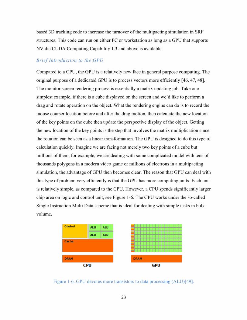
chip area on logic and control unit, see Figure 1-6. The GPU works under the so-called
Single Instruction Multi Data scheme that is ideal for dealing with simple tasks in bulk
volume.
Figure 1-6. GPU devotes more transistors to data processing (ALU)[49].

24
STRUCTURE OF THE CODE
The idea of our GPU based multipacting code is to take the advantage of high
concurrency of the GPU to track millions of particles simultaneously to simulate the
multipacting phenomenon. There are three primary parts in the code.
x Main (Master) Function
The main function is a host function that runs on the CPU and controls the
workflow of the program. All the kernels running on GPU are launched from the
host code. First, the input parameters are read into the main function from an
input file. Then the code reads in the geometry model of the structure and the EM
field distribution from Omega3P Eigensolver. The mesh model will be pre-
processed before it is sent to the GPU so that the particles can be located more
easily when it is going through the tracking process. Then the main function calls
the sequence of the core kernels in the display call back function of the OpenGL
so that the tracking process is synchronized with the rendering process. The core
tracking kernels will be discussed below.
x Momentum Update
Initial locations, momentums and relative RF phases of the particles are generated
by a kernel called init_par on GPU. Then the field strength at the location of the
particle is calculated by using first-order shape function of the tetrahedral element
and the field information on the vertexes of the element in which the particle is
located. After the field information is ready, the momentum-updating kernel takes
the pointer to the segment of global memory that stores the information and starts
calculating the new momenta of the particles. The momentum-update task is done
by a fourth order Runge-Kutta method [50]. After the momenta are updated, the
new location of the particle is also updated as if there is no collision. We call this
a virtual movement of the particle. The further steps will be conducted by the
particle locating kernel, which will be discussed later.
Since momentum updating does not involve memory copying between the GPU
and the CPU, we can save a considerable amount of time. Each momentum-

25
updating kernel requires 90 registers, which still needs some optimization.
However, even with this amount of register requirement a low tier GeForce GTX
860M GPU can run about 50 thousands of the kernels simultaneously and finish
one iteration in about 30 ms for 2 million particles.
x Particle Locating
The code spends a major portion of time on determining the final location of the
particles after each virtual movement. The data structure of the mesh model is
organized so that each mesh element also stores the IDs of the four neighbor
elements as well as the internal ID of the surfaces they shared. Every time after
the particle is virtually moved by the momentum updating kernel, we follow the
procedure of following pseudocode [51, 52]:
Calculate the Barycentric coordinates (B-coords) [53] of the particle in the old
element.
If the particle is still in the old tetrahedral mesh (all B-coords > 0):
Make a real movement on the particle;
Update the momentum of the particle;
Return;
Else:
Calculate the parametric coordinates (a, b) of intersect of the virtual trajectory of
the particle with all four walls of the tetrahedral element it was originally in.
There will be one and only one pair of coordinates that falls in the range 0<a<1,
0<b<1, a+b<1 and the side corresponding to that pair is the side that the virtual
trajectory went through.
If the particle hits a wall for the first time:
Record the ID of the wall hit by the particle;

26
Generate the new momentum of the particle as if it is a new
particle;
Flag the particle as a particle that just hit a wall;
Return;
Else if the particle hits the wall in previous time step:
Flag the particle as dead;
Return;
Else if the particle hit a shared wall:
Update the ID of tetrahedral mesh the particle is located and go
back to the top of the code.
The code keeps a record of how many steps the kernel took to find the particle eventually
and adjust the interval of time step of each particle accordingly. If the kernel took too
long to locate the particle, the time step would be halved in next iteration.
After every particle is either located or registered dead, the master clock advance by one
time step and the EM field is updated.
After every certain amount of time, two RF cycles is set as a default, the master function
calls the memory-copy function to copy the results back from GPU to CPU and perform a
sort method on the flags to get rid of the dead particles so that the following simulation
can focus on the active particles only.
The particle-locating kernel requires significantly more registers (180) and has much
more branching than the momentum update kernel. Both are undesirable for a GPU code.
However, the maximum achievable GFLOPs of this kernel on a Tesla K40 card is still
around 150 which is about three times than an Intel i7 quad-core CPU can provide.
Although there is still ample of space for improvement on the algorithm of this kernel, we
already can see the power of a GPU accelerated code. Figure 1-7 shows the performance
boost of the GPU code compares to the CPU version.

27
Figure 1-7. The performance boost of GPU code.
Simulation results
The location of multipactors is shown in Figure 1-8.
Figure 1-8. Location of MP in the 112 MHz cavity given by (Left) GPU code shown as red dots and (right) Track3P shown as white dots.
The multipacting occurs at a gun voltage equal to 40 kV. In results from both codes, the
resonant particles exhibit two-point multipacting in the corner between exit vertical wall
and the outer conductor of QWR cavity. The highest enhanced counter function is
1 × 10 . This multipacting barrier was observed in the first commissioning after the
cavity was fabricated in Niowave Inc. and quickly conditioned [54].

28
1.3 Tuning: Simulation and Measurements Active Mechanical tuning
The 112 MHz cavity is designed to be compatible with the RHIC system. In order to
match the electron beam to RHIC ion beam, it is essential that the cavity can be tuned to
cover at least 78 kHz [55] around the112 MHz central frequency. A mechanical tuner has
been installed inside the cryomodule. The mechanical deformation was calculated by the
simulation code Ansys and the frequencies of the original and deformed cavity were
calculated by Superfish and CST microwave studio. The simulation shows that the
frequency change rate provided by this tuner is about 14 kHz/mm. This compares well
with the experimental measurement during the first commissioning at Niowave Inc.
which is shown in Figure 1-9.
Figure 1-9. Mechanical Tuning of 112 MHz cavity, the straight line shows linear fitting.
y = -9.763x + 1.7017
-50.00
-40.00
-30.00
-20.00
-10.00
0.00
10.00
20.00
-2.000 -1.000 0.000 1.000 2.000 3.000 4.000 5.000
Freq
uenc
y Sh
ift (k
Hz)
Displacement (mm)
Frequency Tuning

29
Detuning due to Helium pressure change
Another important figure of merit is the sensitivity of cavity frequency to the helium
pressure inside the helium vessel. Due to its high loaded Q (𝑄 ), the SRF cavity is very
sensitive to frequency shift. For example, assume the loaded Q is 1 × 10 and the central
frequency is 112 MHz, then the FWHM of the resonance peak is in the order of 1 Hz.
Therefore the sensitivity of the cavity frequency to the ambient condition, in this case the
helium pressure, is of great importance and requires special consideration when designing
a cavity.
The cavity model is first generated in Ansys, and the pressure boundary condition is
applied to the outer surface of the shell structure. Then the deformation is calculated by
the Multiphysics solver to generate the deformed cavity. Then we export the deformed
cavity to Superfish to calculate the shifted frequency. The simulated frequency sensitivity
due to pressure change is 14 ± 4 Hz/mbar. By pressurizing the helium vessel one can
measure the frequency change as a function of the helium pressure. The experimental
result of the pressure sensitivity is shown in Figure 1-10 [56].
Figure 1-10. Measured cavity frequency shift vs. helium vessel overpressure (measured as mbar above atmospheric pressure).

30
Lorentz Detuning Simulation and Measurement
Another important detuning to the cavity is the so-called Lorentz detuning which is
caused by the RF field stored inside the cavity [57].
The force exerted by the electric field on the cavity wall can be derived in the following
way.
First, we assume the cavity wall to be the perfect conductor, which is a good
approximation for SRF cavities. The field is normal to the wall and the field strength is
constant across a small area. In this case the relation between the field E and the charge
density 𝜎 is
𝐸 =𝜎𝜖. ( 1-36 )
The pressure of Lorentz force generated by electric field (self-field excluded) is
𝑃 =
𝜖 𝐸2
. ( 1-37 )
Similarly, we can derive the pressure from the magnetic field as
𝑃 =
𝜇 𝐻2
. ( 1-38 )
The direction of the electric force is pointing out of the wall surface, and the effect of the
magnetic force is the opposite.
Therefore, the total pressure of Lorentz force is
𝑃 =
𝜇 𝐻2
−𝜖 𝐸2
, ( 1-39 )
where H and E are the effective field strength of magnetic and electric field, respectively.
One thing worth pointing out is the Lorentz detuning to cavity frequency is always
negative. One way to understand this is by looking at a typical pillbox cavity. The electric
field always tends to pull the iris together hence reduce the vacuum volume, in other
words, increase the capacitance and reduce the frequency of the resonator. The magnetic

31
field will push the wall outwards and increase the inductance and again reduce the
resonance frequency. This gives us a qualitative feeling of the Lorentz detuning.
To calculate the frequency shift of the cavity due to its shape distortion (Figure 1-11), the
fundamental formula we need to use is the so-called Slater’s perturbation formula which
can be derived in the following way [26].
Figure 1-11. Original cavity volume (left) and deformed cavity (right).
From the Maxwell’s equations, we get the curls of the electric and magnetic field as
following: (All the symbols for field are vectors if not specified.)
∇ × 𝐸 = −𝑗𝜔 𝜇𝐻 ,
∇ × 𝐻 = 𝑗𝜔 𝜖𝐸 ,
∇ × 𝐸 = −𝑗𝜔𝜇𝐻,
∇ × 𝐻 = 𝑗𝜔𝜖𝐸.
( 1-40 )
Here we use j as the imaginary unit, 𝜔 is the frequency of the EM field. Quantities with
subscript 0 means they are the original ones. Take the conjugate of first one and multiply
it with 𝐻, and multiply the last one with 𝐸∗ we get
𝐻 ∙ ∇ × 𝐸∗ = 𝑗𝜔 𝜇𝐻 ∙ 𝐻∗,
𝐸∗ ∙ ∇ × 𝐻 = 𝑗𝜔𝜖E∗ ∙ 𝐸. ( 1-41 )
Use the first to subtract the second one in (1-41)
𝐻 ∙ ∇ × 𝐸∗ − 𝐸∗ ∙ ∇ × 𝐻 = 𝑗𝜔 𝜇𝐻 ∙ 𝐻∗ − 𝑗𝜔𝜖E∗ ∙ 𝐸. ( 1-42 )
Notice the LHS is the identity of ∇ ∙ (𝐸∗ × 𝐻) we get
dV
𝐸 ,𝐻
𝜔 , 𝑉
𝐸, 𝐻
𝜔, 𝑉

32
∇ ∙ (𝐸∗ × 𝐻) = 𝑗𝜔 𝜇𝐻 ∙ 𝐻∗ − 𝑗𝜔𝜖𝐸∗ ∙ 𝐸. ( 1-43 )
Similarly, we can get
∇ ∙ (𝐸 × 𝐻∗) = −𝑗𝜔𝜇𝐻 ∙ 𝐻∗ + 𝑗𝜔 𝜖𝐸∗ ∙ 𝐸. ( 1-44 )
Add the equation ( 1-43 ) with ( 1-44 ) and integrate over the new volume of the cavity
we can get
∇ ∙ (𝐸∗ × 𝐻) + ∇ ∙ (𝐸 × 𝐻∗) 𝑑𝑉 = (𝐸∗ × 𝐻) + (𝐸 × 𝐻∗) ∙ 𝑑𝑆
= (𝐸∗ × 𝐻) ∙ 𝑑𝑆 = 𝑗(𝜔 − 𝜔 ) (𝜇𝐻 ∙ 𝐻∗ + 𝜖𝐸 ∙ 𝐸∗)𝑑𝑉.
( 1-45 )
The second step can be obtained by noticing 𝐸 × 𝑑𝑠 = 0, namely using the perfect
conductor condition.
Since the perturbed surface 𝑆 = 𝑆 − Δ𝑆, we can rewrite the LHS of ( 1-45 ) as
(𝐸∗ × 𝐻) ∙ 𝑑𝑆 = (𝐸∗ × 𝐻) ∙ 𝑑𝑆 − (𝐸∗ × 𝐻) ∙ 𝑑𝑆
= − (𝐸∗ × 𝐻) ∙ 𝑑𝑆.
( 1-46 )
Similar to the argument above, by using 𝐸 × 𝑛 = 0 on 𝑆 we got rid of the first term
after first equal sign.
Plug equation ( 1-46 ) into to ( 1-45 ) we can get the expression of frequency shift as
𝜔 − 𝜔 = −
𝑗 ∮ (𝐸∗ × 𝐻) ∙ 𝑑𝑆
∮ (𝜇𝐻 ∙ 𝐻∗ + 𝜖𝐸 ∙ 𝐸∗)𝑑𝑉. ( 1-47 )
If we assume 𝛥𝑉 and 𝛥𝑆 to be small and take approximation 𝐸 ≈ 𝐸 , 𝐻 ≈ 𝐻 , we can
find
(𝐸∗ × 𝐻) ∙ 𝑑𝑆 ≈ (𝐸∗ × 𝐻 ) ∙ 𝑑𝑆. ( 1-48 )
33
Equation ( 1-48) is the well known integral of Poynting’s vector across an enclosed
surface. When there are no losses, the Poynting vector integral across the enclosed
surface is simply
(𝐸∗ × 𝐻 ) ∙ 𝑑𝑆 = 𝑗𝜔 (𝜇𝐻 − 𝜖𝐸 )𝑑𝑉. ( 1-49 )
Plug back to equation ( 1-47 ) we will get
𝜔 − 𝜔𝜔
=∮ (𝜇𝐻 − 𝜖𝐸 )𝑑𝑉
∮ (𝜇𝐻 + 𝜖𝐸 )𝑑𝑉. ( 1-50 )
Again, the volume within which magnetic field dominates will expand as we discussed
before, this gives us a negative 𝛥𝑉 if we follow the definition we used here and for the
strong electric field part we get positive 𝛥𝑉. Hence, the overall effect from both parts is
reducing the frequency of the cavity.
In practice, we use the numerical code to simulate the sensitivity of cavity to Lorentz
detuning effect in a similar manner to what we applied above in carrying out the pressure
sensitivity analysis.
The steps described below apply to CST 2014 and 2015.
First, we build a real shell model of the cavity and the vacuum volume of the cavity.
Then we calculate the field distribution of the interested Eigen mode of the cavity. In this
step, we use only the vacuum volume of the cavity and disable the shell part.
Next, we use the internally built Lorentz force processor in the High Frequency (HF)
solver of CST package to generate the Lorentz force distribution from the field
distribution.
Then we create a new project in the mechanical simulation solver, namely the
Multiphysics solver. This new project contains the same geometries as the HF one but
with shell activated and vacuum disabled. The deformation of the shell is then calculated
with the Lorentz force field imported from the HF solver.

34
Finally, we go back to the first project and import the deformation from the Multiphysics
solver and do the sensitivity analysis to get the new frequency.
Figure 1-12 shows the deformation of the cavity when gun voltage is 2 MV.
Figure 1-12. Deformation of the cavity when gun voltage equals to 2 MV.
The frequency shift due to this deformation is −746 ± 6 Hz. Hence the Lorentz detuning
sensitivity is 186 ± 1.5 Hz/MV . This amount of detune can be easily tuned back by
active tuner.
1.4 Summary In this chapter, we discussed the design of the 112 MHz cavity. We listed and derived
several important figures of merit in cavity design such as center frequency, the quality
factor, the geometry factor, the R/Q, the maximum field ratios Bmax/Eacc and Emax/Eacc, and
the transit time factor. The designed parameters are presented in this chapter. We chose
the QWR cavity so that the cavity can be made compact for 112 MHz frequency.
Although we sacrificed the shunt impedance R/Q and the maximum field ratios by
choosing this shape, we gained the advantage of a realistic cavity size, a longer
acceptable beam bunch length and a larger bunch charge. The multipacting phenomenon
was discussed in detail, and a GPU accelerated code was written by the author to increase
the productivity of multipacting simulation. Simulation results from both GPU code and
Track3P show that the multipacting in the cavity is not problematic. The sensitivity of
cavity to the helium pressure and Lorentz detuning was also discussed in the second half
of the chapter. The simulation results and experimental measurements are consistent with
each other.

35
2 Fundamental Power Coupler (FPC) / Fine Tuner Design and Fabrication
Due to the geometric limitation in the cavity which was built for a different purpose, we
decided to use the coaxial structure fundamental power coupler (FPC). The main purpose
of the FPC is, of course, providing the RF power to the cavity and beam. However by
adjusting the position of the FPC, we can also adjust the frequency of the cavity and thus
provide a fine tuning mechanism for the injector. The deviation of the external coupling
of the FPC, due to the fine tuning action from its optimal value is small and can be easily
compensated by adjusting the RF drive power. When we were designing the FPC, the
first thing we had to consider was the capability of the FPC. Namely, whether we can
provide enough power to the beam, or in other words can we get enough coupling.
Another issue is whether or not we need an active cooling for the FPC. The coaxial
structure provides strong coupling and potentially generate a significant amount of RF
loss on its surface, and this heating has to be closely studied. The third issue of the FPC is
the multipacting study, which will be discussed later in this chapter.
2.1 RF Design of the FPC The fundamental power coupler is a coaxial type coupler similar to the one used in the
Naval Postgraduate School (NPS) gun [58]. The coupler is attached to beam exit port of
the SRF gun. Its hollow center conductor, or coupling tube, allows the beam to go
through. Adjusting the penetration of the coupling tube towards the acceleration gap
allows us to tune the cavity resonant frequency as well as keep the coupling strength in a
good range. Figure 2-1 illustrates the FPC attached to the SRF gun port. The main
parameters of the fundamental power coupler are listed in Table 2-1.
Table 2-1. Parameters of the fundamental power coupler
Frequency tuning range by FPC 4.5 kHz
Travel range 40 mm
Qext, min. 1.25107
Max. RF power loss on the inner conductor 899 W
Max. RF power loss on the outer conductor 555 W

36
Figure 2-1. Cross-section of the FPC attached to the beam exit port (top view).
To enhance its ability to change the cavity’s frequency, the FPC [7] is designed as a
resonant quarter wavelength structure slightly detuned down, by ~2.8 MHz, from the
cavity resonance. There are significant RF fields inside the normal-conducting coupler
structure, which generate much larger losses than those inside the superconducting cavity,
especially when fully inserted. Figure 2-2 shows the variation of the gun’s FPC external
quality factor versus the position of the coupling tube relative to the cavity (blue line).
This result is calculated with CST Microwave Studio. The range of 𝑄 is from 5×10⁶ to
1.2×10⁸. The bunch charge can be supported by this FPC at full RF power is from 1 nC
to 5 nC given the repetition rate of bunch of 78 kHz. Considering the gun voltage which 2
MV, the maximum beam power is 780 W.
RF windows
Connection to linear motion system Nb cavity
Copper center conductor
Copper plated outer conductor stainless steel
bellows

37
Figure 2-2. Qext versus position of the coupling tube.
Also shown in Figure 2-2 are the plots of the optimal (no reflection) external quality
factor for three values of the bunch charge under the assumption that there is no parasitic
detuning due to microphonic noise. The optimal external 𝑄 is calculated using the
following equation [30]:
𝑄 _ =𝑄
1 + 𝑃𝑃
=𝑄
1 + 𝑓 ∙ 𝑞 ∙ 𝑉 ∙ cos𝜑𝑉 (𝑅 𝑄⁄ ∙ 𝑄 )⁄
( 2-1 )
where 𝑄cav is the cavity quality factor, which accounts for losses in the cavity walls,
cathode stalk and FPC; Pbeam is the power delivered to beam; Pcav is the power dissipated
in the cavity, cathode stalk and FPC; fb is the bunch repetition rate; qb is the bunch charge;
Mb is the bunch phase. The bunch is assumed to be on crest for plots shown in Figure 2-2.
As one can see from the plots, depending on the FPC position and bunch charge we
would need 𝑄 from 107 to 108 for optimal matching. By adjusting the position of the
FPC we can also fine-tune the frequency of the cavity. The tuning range is shown in
Figure 2-3.

38
Figure 2-3. Frequency tuning by FPC.
2.2 Thermal Analysis One important topic that deserves special consideration is the thermal load of the FPC
due to the high RF power loss on its inner conductor. As given in Table 2-1, the
maximum RF power loss on the inner conductor is nearly 900 W. Since the inner
conductor connects only with the outer conductor at the far end of the FPC, the thermal
conductance of the inner conductor is not enough to keep it at a low enough temperature.
Figure 2-4 shows the temperature map of the FPC if there is no active water-cooling.

39
Figure 2-4. Temperature map of FPC without active water cooling.
As we can see the maximum temperature at the tip of the coupling tube is nearly 732 K.
Given that the coupling tube and cold cavity wall overlap along a distance of 2 cm, the
radius of the coupling tube is 4 cm and the emissivity of the gold plated surface is 0.02,
we can use the Stefan-Boltzmann [59] equation to estimate the radiation thermal load:
𝑃 = 𝑒𝜎𝐴(𝑇 − 𝑇 )
= 0.02 × 5.6703 × 10 × 2 𝜋 × 0.04 × 0.02 × (732 − 4.5 )
= 1.6 𝑊,
( 2-2 )
where e is the emisssivity of the tub, 𝜎 is Stefan-Boltzmann constant, 𝑇 is the
temperature of the tube and 𝑇 is the temperature of the cavity. the This value coresponds
to a 13% increase in the thermal load of the cryosystem.
If we include the water cooling system, the temperature of the FPC can be well controlled
at 293 K. Figure2-5 shows the temperature map of FPC with active water cooling. The
extra thermal load to the cryosystem from the tip of the FPC will be reduced to merely
0.25 W.

40
Figure 2-5. Temperature map of FPC with active water cooling.
In order to reduce the emissivity of the FPC inner conductor, we plated the copper tube
with gold. The emissivity of copper and gold can be found in Table 2-2 [60]. We can
clearly see the advantage of gold plating here. Even if the copper stays in its best
condition, it still emits 50% more heat to the cryomodule. Considering the reactiveness of
the pure copper, it is difficult to prevent the oxidization to the surface which will be
devastating to the liquid helium system. Therefore, we decided to gold plate the FPC to
reduce the thermal emission as much as possible and eliminate the risk of an increase in
the emissivity due to oxidation.
Table 2-2. Emissivity of copper and gold
Copper (highly polished) 0.03
Copper (Oxidized) 0.78
Gold (polished) 0.02
2.3 Multipacting Study The multipacting simulation in FPC is performed with GPU code and Track3P. One
multipacting barrier is found around 200 keV inside the FPC, which has the similar
strength as the one we discussed in the cavity part. The location of the multipacting
barrier is shown in Figure 2-6. This is a two-point first-order multipactor, and the
enhanced counter function is around 107. As a matter of fact, the gold plating on the FPC
also reduces the MP strength due to the lower secondary electron yield as shown in
Figure 2-7.
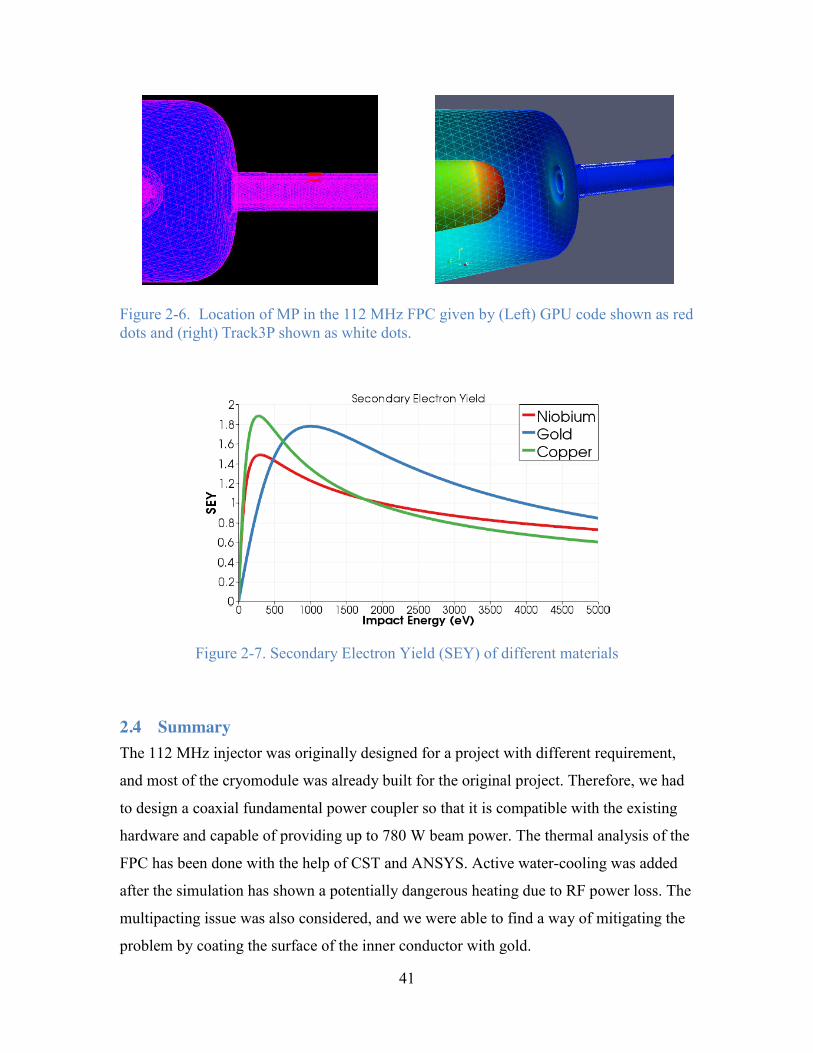
41
Figure 2-6. Location of MP in the 112 MHz FPC given by (Left) GPU code shown as red dots and (right) Track3P shown as white dots.
Figure 2-7. Secondary Electron Yield (SEY) of different materials
2.4 Summary The 112 MHz injector was originally designed for a project with different requirement,
and most of the cryomodule was already built for the original project. Therefore, we had
to design a coaxial fundamental power coupler so that it is compatible with the existing
hardware and capable of providing up to 780 W beam power. The thermal analysis of the
FPC has been done with the help of CST and ANSYS. Active water-cooling was added
after the simulation has shown a potentially dangerous heating due to RF power loss. The
multipacting issue was also considered, and we were able to find a way of mitigating the
problem by coating the surface of the inner conductor with gold.

42
3 Cathode and Insertion System The photocathode’s Quantum Efficiency (QE) drops significantly with temperature as
reported [61,62]. To avoid this degradation, we designed 112 MHz SRF injector with a
cathode operating at room temperature. K2CsSb photoemission layer is deposited on the
mirror-finished front surface of a 20-mm diameter molybdenum puck. The cathode
resides inside a cathode stalk and is inserted into the injector when needed with a
specially designed cathode manipulation system. The cathode stalk, which will be
discussed in more detail later, is permanently installed inside the gun to avoid
unnecessary particulate contamination to the cavity. The stalk serves two functions: 1)
thermally insulates the cold QWR cavity from the cathode, and 2) provides an RF choke
joint between the cathode and the cavity. The latter minimizes the transverse electric field
near the cathode thus improving the beam quality. Detailed design considerations of the
cathode stalk, cathode preparation, and manipulation are discussed below.
3.1 Cathode Stalk Design The cathode-stalk design principles are similar to that described in [58]. The stalk is a
hollow normal conducting structure made of copper-plated (25 𝜇m) stainless steel. It does
not have direct physical contact with the cold center conductor of the cavity hence
reducing the thermal load to the cavity and allowing the stalk to operate at room
temperature. To reduce its emissivity, we coated the stalk with a very thin, about one
micrometer, layer of gold. A Rexolite® “spider” is utilized to center the cantilevered stalk
inside the cavity. However, this design allows the RF field to propagate out of the cavity
into a gap between the stalk and the nose cone of the cavity. A half-wavelength stalk
shorted at the far end makes a choke filter which reduces RF field penetration and
minimizes the voltage drop between the cathode and the cavity’s center conductor. The
gap between the stalk and nose cone at the entrance of the cavity is only 3.56 mm. The
stalk length was shortened to account for the capacitance created by this small gap. The
resulting electric field distribution near the cathode is shown in Figure 3-1.

43
Figure 3-1. (Upper): Electric field distribution near the cathode surface and nose cone (gap between the cathode and stalk is not shown.);; (Lower): Transverse field distribution on cathode before (♦) and after () optimization.
0.00E+00
1.00E-01
2.00E-01
3.00E-01
4.00E-01
5.00E-01
6.00E-01
7.00E-01
8.00E-01
9.00E-01
0.03
0.08
0.13
0.18
0.22
0.27
0.32
0.37
0.42
0.46
0.54
0.56
0.66
0.68
0.78
0.80
Er(M
V/m
)
R (cm)
Er vs. R
Original
Optimized

44
The transverse electric field on the cathode’s surface was reduced by optimizing the
length of the stalk as well as changing the position of the tip of the stalk relative to the
cavity. By integrating along the solid black line shown in Figure 3-1, we can get the
voltage drop between the cathode and cavity, which is only 0.22 kV at an accelerating
voltage of 2 MV. So far we are talking about a cathode stalk that has the uniform
diameter after the first chamfer behind the cathode tip. The RF power loss on this
uniform stalk is 36 W.
Further reduction of RF losses from 36 W to 20 W on the stalk is achieved by introducing
an impedance mismatch in the middle of the stalk (as shown in Figure 3-2), which creates
a quarter wavelength impedance transformer.
Figure 3-2. Cathode stalk assembly.
Since the shorted end has finite impedance 𝑍 , a real half wave stalk will propagate this
impedance to the gap between the cathode and cavity as indicated by following lossless
transmission line equation.
𝑍 = 𝑍
𝑍 + 𝑗𝑍 tan(𝛽𝑙)𝑍 + 𝑗𝑍 tan(𝛽𝑙)
, ( 3-1 )
where 𝑍 is the impedance of the stalk seen by the cavity, 𝑍 is the characteristic
impedance of the stalk-cavity structure, j is the imaginary unit and 𝛽 = and 𝑙 is the
length of the stalk. If 𝑙 = we will have 𝑍 = 𝑍 which can be further reduced if we
stainless steel tubes plated with 25 microns of copper and 1 micron of gold
2” stalk tube section
3” stalk tube section
center support
water connections

45
introduce the impedance mismatch in the middle of the stalk. Consider the following
schematic model:
Figure 3-3. Quarter wave transformer.
In this scheme, the impedance 𝑍 is further reduced as
𝑍 = 𝑍𝑍 𝑍 + 𝑖𝑍 tan(𝛽𝑙)𝑍 + 𝑖𝑍 tan(𝛽𝑙) + 𝑖𝑍 tan(𝛽𝑙)
𝑍 + 𝑖𝑍 𝑍 + 𝑖𝑍 tan(𝛽𝑙)𝑍 + 𝑖𝑍 tan(𝛽𝑙) tan(𝛽𝑙)
, 𝑙 =𝜆4
=𝑍𝑍
𝑍 .
( 3-2 )
Since the characteristic impedance of coax is 60 ln ( ) where R is the radius of outer
conductor and r is the radius of inner conductor, we always have < 1. Therefore we
reduced the impedance of the stalk seen by the cavity and consequently reduced the
voltage drop between the stalk and the cavity. Another advantage of the impedance
mismatch is the reduction of power loss on the alignment bellows, which could overheat
if the RF loss stayed as high as the original number. The remaining heat is removed by
cooling water. Table 3-1 compares RF losses on different parts of the stalk assembly
(shown in Figure 3-4) between a uniform stalk design and a stalk with impedance
transformation step.
𝑍
𝑍 𝑍 𝑍
𝜆4
𝜆2

46
Figure 3-4. Assembly of 112 MHz SRF QWR Injector.
Table 3-1. Comparison of RF losses on a uniform stalk and a stalk with an impedance transforming step at an accelerating voltage of 2 MV.
Power losses Uniform stalk
Stalk with impedance transformation step
On the stalk (Au) 36 W 20 W
On the bellows (Cu) 28 W 7 W
On the Nb pipe 120 𝜇W 31 𝜇W
3.2 Cathode Preparation We chose K2CsSb because of its high quantum efficiency (QE) in green light and long
lifetime in a 10-10 Torr scale vacuum environment. Using 532 nm green light makes it
easier to get a high-power laser and to shape the laser pulses spatially and temporally.
The cathodes are prepared in a deposition chamber described in [63] and shown in Figure
3-5. The deposition chamber is equipped with a residual gas analyzer (RGA), a quartz
crystal film thickness monitor, and multiple viewports for observation and laser
illumination of the cathode. Alkali metal dispenser sources (SAES getter 6 mg K and
10.8 mg Cs) and Antimony (Goodfellow 99.999% purity pellets) are used for the
deposition. These sources are installed separately and inserted through gate valves into
the deposition chamber as needed during evaporation. A boron nitride resistive heater is
used to control the substrate temperature over the range of 20qC to 500qC.
Alignment bellows

47
Figure 3-5. Multi-alkali deposition system for the 112 MHz gun.
The cathode material is deposited onto a high purity molybdenum puck. The puck’s front
surface is mirror-finished to 2 nm RMS roughness to reduce the roughness-induced
emittance [64, 65, 66, 67]. Figure 3-6 shows molybdenum pucks before cathode
deposition. We use standard cathode deposition procedure, which is discussed in [68].
Two cathodes were prepared with an initial QE at 6.5% and 8%, respectively.
Figure 3-6. Photograph of polished molybdenum pucks before deposition of the photoemission layer.
Cs K Sb
Deposition
Chamber

48
3.3 The Cathode Insertion System The cathode insertion system is depicted in Figure 3-7. The insertion system with up to
three cathodes inside is connected to the gun via a load lock. The cathode diagnostic
system allows us to measure the cathode’s QE before insertion. The cathode end
assembly, attached to the manipulator arm, is shown in Figure 3-8. The manipulator arm
has three centering standoffs with rolling ceramic wheels, which prevent damage to the
cathode on insertion and limit generation of particulates. Two grooves on the cathode
puck allow manipulation with special spring “forks”. Finally, gold plated RF spring
finger contacts ensure that EM field does not propagate into the cathode stalk.
Figure 3-7. Cross-sectional view of the cathode insertion system.
Stalk assembly
Kinematic stalk stop
External stalk ion pump
Cooling line interface
Internal stalk ion pump Cathode diagnostic section
Portable in-vacuum injection system

49
Figure 3-8. Cathode end assembly.
3.4 Multipacting Study The multipacting simulations done by GPU code and Track3p show that there is a
relatively strong MP barrier inside the gap between cathode stalk and the outer conductor.
The multipacting begins to build up at around 600 kV gun voltage (shown in Figure 3-9)
and persists until up to 1 MV gun voltage. The strength of this MP is about 4 orders of
magnitude higher than the one in the FPC. Gold plating helps to reduce the maximum
enhanced counter function. If TiN coating were used, the MP could be suppressed even
further as shown in Figure 3-10.
Figure 3-9. Multipactors between the cathode stalk and the cavity. The MP appears at around 600 kV gun voltage.
Centering standoffs
Interface with manipulator arm
Cathode puck with two groves
Gold plated RF spring finger contacts

50
Figure 3-10. Enhanced counter function of MP in cathode stalk with copper surface, gold plating and TiN coating.
3.5 Summary We can routinely grow K2CsSb cathode with QE better than 5% in the deposition
chamber at the Instrumentation Department at BNL. To preserve the QE of cathode we
need to, ideally, keep it under vacuum better than 1 × 10 Torr. Therefore, we built a
cathode transport system which can take up to three cathodes from the deposition
chamber to the 112 MHz injector in RHIC tunnel while keeping the vacuum under
1 × 10 Torr. We also discussed the design and test result of a half-wavelength choke
structure cathode stalk in this chapter. The stalk allows us to operate the cathode at room
temperature so that the QE at the wavelength of 532 nm will not suffer degradation due to
cryogenic temperature. The design of the stalk also reduces the voltage drop between the
cathode and the cavity because of the choke structure. We also showed an impedance
mismatch which further reduces the impedance of the choke structure seem by the cavity
and consequently reduce the voltage drop in the cathode-cavity gap and minimizes the
heat load on the stalk. The multipacting issue is the main problem for this design. We
tried to reduce the enhanced counter function by coating the stalk with gold. This also
reduces the emissivity of the surface hence reduces the thermal load from radiation to the
cryosystem. Simulation results show promising improvement by this surface treatment.
Further improvement to this issue can be achieved by coating the surface with TiN.
1.00E+001.00E+031.00E+061.00E+091.00E+121.00E+151.00E+18
600 700 800 900 1000 1100Ehan
ced
Co
un
ter
fun
ctio
n
Impact Energy/eV
Enhanced Counter Functions
Copper
Gold
TiN

51
4 Beam Dynamics Simulation The electron beam is generated by the multi-alkali photocathode K CsSb under the
illumination of 532 nm laser. The initial bunch length in time domain is determined by
the laser pulse. The typical quantum efficiency of the cathode is on the order 5%. And the
bunch charge deliverable by 112 MHz can be as high as 5 nC. Three parameters are of
most interest to the CeC PoP application: The peak current, the normalized emittance and
the energy spread of the beam [1, 69, 70]. The peak current is simply the bunch charge
divided by the bunch duration, and energy spread is just the standard deviation of the
energy of particles in a bunch normalized to the mean energy. The emittance is a concept
that deserves a little more explanation.
4.1 Emittance of a Beam The emittance of the beam is a figure of merit used regularly in the accelerator
community to describe the quality of the beam. The emittance is of great importance in
many applications such as colliding beams, free electron laser, electron cooling, etc. We
use the statistical definition here. The definition of the emittance is [71]:
𝜖 = ⟨𝑥 ⟩⟨𝑥 ⟩ − ⟨𝑥𝑥 ⟩ , ( 4-1 )
where the bracket ⟨ ⟩ means taking the average of the variable in it. This definition of
the emittance represents the statistical area of the x-x’ phase space occupied by the beam.
Here x is the transverse coordinate of the particle and x’ is the diverging angle of the
particle:
𝑥 =𝑝𝑝. ( 4-2 )
As one can see, the geometrical emittance 𝜖 defined in this way will diminish rapidly
when the electron is accelerated from rest to near speed of light. On the other hand the
normalized emittance is a conserved quantity in a Hamiltonian system:
𝜖 = 𝜖 𝛽𝛾, ( 4-3 )
where 𝛽 and 𝛾 are Lorentz factors calculated from the average energy of the bunch and
𝜖 is the unnormalized, or geometrical emittance defined in equation (4-1).

52
The emittance is very important in many applications. For example in Free Electron
Laser facility, to get transverse coherent radiation the un-normalized emittance must
satisfy the following condition:
𝜖 <
𝜆4𝜋
. ( 4-4 )
Recalling the divergence of laser [72]
𝜃 =
𝜆𝜋𝑤
, ( 4-5 )
where 𝑤 is the waist size of the laser beam and 𝜆 is the wavelength of the laser. We can
interpret the physical meaning for the requirement in (4-4) as: the emittance of the
electron beam needs to be smaller than ¼ of the laser emittance [73].
There are many sources that determine the value of the emittance [74]. The most
important three components of the emittance as produced in an RF injector are the
thermal emittance 𝜖 , The RF induced emittance 𝜖 and the space charge induced
emittance 𝜖 . Assuming that these emittances are uncorrelated, the total emittance can be
calculated as follows:
𝜖 = 𝜖 + 𝜖 + 𝜖 +⋯ ( 4-6 )
The thermal emittance is the emittance of the beam right after the bunch is generated
from the surface of the cathode, thus it is a fundamental limit on the magnitude of the
total emittance. In order to discuss the thermal emittance, we need to have a closer look at
the mechanism of photoemission of electrons from a photocathode.
The photoemission process can be decomposed into three major steps according to the
model first proposed by Spicer [75, 76]. In the first step, the photons excite the electrons
in the photocathode material. In a semiconductor this process excites electrons from the
valence band to the conduction band. In the second step, the excited electrons drift to the
surface of the cathode, accompied by various types of scattering events. The third step is
the emission step during which the electrons overcome the potential barrier between the

53
cathode and vacuum and exit the cathode. One simple model of the process is illustrated
in Figure 4-1.
Figure 4-1. Three-step model for the metal cathode.
In the first step, the bound electrons absorb the energy of the photons. We assume only
the portion of electrons that have energy higher than the cathode-vacuum potential barrier
right after the excitation can escape the barrier. Then this portion can generally be written
as the following:
𝑃 = 𝑑𝐸𝑁(𝐸 + ℏ𝜔) 1 − 𝑓 (𝐸 + ℏ𝜔) 𝑁(𝐸)𝑓 (𝐸)
ℏ. ( 4-7 )
𝐸
𝐸 + 𝜙 − ℏ𝜔e-
e- e- e-
1
2 3
ℏ𝜔
𝜙
𝐸 + ℏ𝜔
54
E is the electron energy, 𝐸 is the Fermi level of the cathode material, 𝜙 is the effective
barrier height between the cathode and vacuum, ℏ𝜔 is the photon energy. Equation (4-7)
is just the convolution of electron distribution in the initial stage 𝑁(𝐸) and available
states distribution in the final stage N(E+ℏ𝜔), with 𝑓 as the Fermi-Dirac distribution.
In the second step the electrons go through different scattering processes and thermalize
to the final distribution rather quickly, at a time of the order of a picosecond. The third
step is the one that we interested the most, which is directly related to the thermal
emittance of the beam. When the electrons reach the barrier between the cathode and
vacuum, they must have enough energy to escape. Under a classical approximation, the
momentum of the electron must satisfy the following condition:
𝑝2𝑚
> 𝐸 + 𝜙 , ( 4-8 )
where 𝑝 is the normal component of the momentum of the electron, 𝑚 is the
effective mass of the electron.
Assume the angle between the normal direction of the surface and the direction of the
momentum of the electron is 𝜃, then we have the maximum incident angle under which
the electron can successfully emit satisfies
cos (𝜃 ) =
𝑝𝑝
=𝐸 + 𝜙𝐸 + ℏ𝜔
. ( 4-9 )
Here 𝑝 is the amplitude of the momentum of electron at emission surface.
After obtaining this, we can calculate the average square transverse momentum as
⟨𝑝 ⟩ =
∭𝑔(𝐸, 𝜃, 𝜙)𝑝 𝑑𝐸𝑑(cos𝜃)𝑑𝜙∭𝑔(𝐸, 𝜃, 𝜙)𝑑𝐸𝑑(cos𝜃)𝑑𝜙
. ( 4-10 )
The 𝑔-function depends on the distribution right after the emission, for example in a
simplified model for metal we can use step function for energy distribution as the
approximation to the Fermi-Dirac distribution at room temperature.
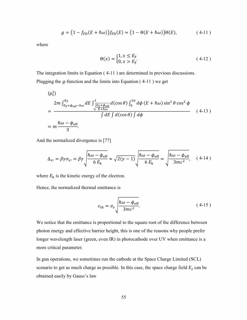
55
𝑔 = 1 − 𝑓 (𝐸 + ℏ𝜔) 𝑓 (𝐸) ≈ 1 − Θ(𝐸 + ℏ𝜔) Θ(𝐸), ( 4-11 )
where
Θ(𝑥) = 1, 𝑥 ≤ 𝐸0, 𝑥 > 𝐸 . ( 4-12 )
The integration limits in Equation ( 4-11 ) are determined in previous discussions.
Plugging the 𝑔-function and the limits into Equation ( 4-11 ) we get
⟨𝑝 ⟩
=
2𝑚∫ 𝑑𝐸ℏ ∫ 𝑑(cos 𝜃)ℏ
∫ 𝑑𝜙 (𝐸 + ℏ𝜔) sin 𝜃 cos 𝜙
∫𝑑𝐸 ∫𝑑(cos 𝜃) ∫ 𝑑𝜙
= 𝑚ℏ𝜔 − 𝜙
3.
( 4-13 )
And the normalized divergence is [77]
Δ = 𝛽𝛾𝜎 = 𝛽𝛾
ℏ𝜔 − 𝜙6 𝐸
≈ 2(𝛾 − 1)ℏ𝜔 − 𝜙
6 𝐸=
ℏ𝜔 − 𝜙3𝑚𝑐
, ( 4-14 )
where 𝐸 is the kinetic energy of the electron.
Hence, the normalized thermal emittance is
𝜖 = 𝜎
ℏ𝜔 − 𝜙3𝑚𝑐
. ( 4-15 )
We notice that the emittance is proportional to the square root of the difference between
photon energy and effective barrier height, this is one of the reasons why people prefer
longer wavelength laser (green, even IR) in photocathode over UV when emittance is a
more critical parameter.
In gun operations, we sometimes run the cathode at the Space Charge Limited (SCL)
scenario to get as much charge as possible. In this case, the space charge field 𝐸 can be
obtained easily by Gauss’s law

56
𝐸 =𝜎𝜖
, ( 4-16 )
where 𝜎 is the charge density under space charge limit, 𝜖 is vacuum permittivity.
Assume the uniform distributed in transverse direction, and the beam has a radius equal
to 𝑎, then
𝑎 =
𝑄𝜖𝜋𝐸
, ( 4-17 )
where 𝑄 is the total charge in a bunch. The space charge limited emittance can be
found as
𝜖 =
𝑄 (ℏ𝜔 − 𝜙 )4𝜋𝜖 𝑚𝑐 𝐸
. ( 4-18 )
Another important source of emittance is the RF cavity induced emittance. This
emittance is the result of a time-dependent transverse kick the bunch receives from the
RF field at the exit of the gun cavity. The transverse RF field at the axis can be evaluated
by Panofsky-Wenzel theorem [78]:
𝐸 = −
𝑟2𝜕𝜕𝑧
𝐸 , 𝑐𝐵 =𝑟2𝑐
𝜕𝜕𝑡 𝐸 , ( 4-19 )
where 𝐸 , 𝐸 are the transverse and longitudinal components of the electric field and 𝐵
is the azimuthal components of the magnetic field. Assume the form of longitudinal
electric field is 𝐸 = 𝐸 (𝑧) cos(𝑘𝑧) sin(𝜔𝑡 + 𝜙 ), the transverse kick of the RF field to
the beam is

57
𝐹 = 𝑒𝑟 −
12𝑑𝐸 (𝑧)𝑑𝑧
cos(𝑘𝑧) sin(𝜔𝑡 + 𝜙 )
−𝑘2𝐸 (𝑧)sin(𝑘𝑧) sin(𝜔𝑡 + 𝜙 )
−𝛽2𝑐
𝐸 (𝑧) cos(𝑘𝑧)𝜔 cos(𝜔𝑡 + 𝜙 )
= 𝑒𝑟 −12𝑑𝐸 (𝑧)𝑑𝑧
cos(𝑘𝑧) sin(𝜔𝑡 + 𝜙 )
−𝑘2𝐸 (𝑧)sin(𝑘𝑧) sin(𝜔𝑡 + 𝜙 )
−𝛽2𝑐
𝐸 (𝑧) cos(𝑘𝑧)𝜔 cos(𝜔𝑡 + 𝜙 )
−𝛽2𝑑𝐸 (𝑧)𝑑𝑧
sin(𝑘𝑧) cos(𝜔𝑡 + 𝜙 )
+𝛽2𝑑𝐸 (𝑧)𝑑𝑧
sin(𝑘𝑧) cos(𝜔𝑡 + 𝜙 )
= 𝑒𝑟 −12𝑑𝐸 (𝑧)𝑑𝑧
cos(𝑘𝑧) sin(𝜔𝑡 + 𝜙 )
−12𝑐
𝑑𝑑𝑡 (𝐸 (𝑧) sin(𝑘𝑧) cos(𝜔𝑡 + 𝜙 )
+𝛽2𝑑𝐸 (𝑧)𝑑𝑧
sin(𝑘𝑧) cos(𝜔𝑡 + 𝜙 ) .
( 4-20 )
The second term goes to zero in the integrated momentum change. The first and third
term are only none zero when there is a jump in 𝐸 (𝑧). Assume step shape of 𝐸 at the
exit of the cavity, we can get the transverse momentum kick as
Δ𝑝 = 𝑟𝑒𝐸2𝑚𝑐
(𝛽 cos(𝑘𝑧 ) sin(𝜔𝑡 + 𝜙 ) − sin(𝑘𝑧 ) cos(𝜔𝑡 + 𝜙 )). ( 4-21 )
Where 𝑧 is the z coordinate of cavity exit and 𝑡 is the time when electron leaves the
cavity.
Assuming the 𝛽 = 1 we have

58
Δ𝑝 = 𝑟𝑒𝐸2𝑚𝑐
sin(𝜔𝑡 + 𝜙 − 𝑘𝑧 ) = 𝑟𝑒𝐸2𝑚𝑐
sin 𝜙 . ( 4-22 )
Namely, the transverse kick is related to the exit phase 𝜙 = (𝜔𝑡 + 𝜙 − 𝑘𝑧 ) of the
particle.
For a Gaussian beam with RMS bunch length equal to 𝜎 exiting the cavity at 𝜙 = ,
the RF induced emittance is [79, 80]
𝜖 =
𝑒𝐸2𝑚𝑐
⟨𝑥 ⟩𝜎
√2. ( 4-23 )
Recall Equation (4-6), the third source of emittance is the space charge induced emittance.
Consider the bunch that under laminar flow, which means the trajectories of the particles
never cross. We slice the bunch into short slices and consider the slices independently.
When the bunch is long, namely the aspect ratio r/L is small in its rest frame, we have the
transverse electric field as
𝐸 =𝐼𝑟
2𝜋𝜖 𝑅 𝑣 , ( 4-24 )
where 𝐼 is the current of the beam, 𝑟 is the transverse coordinate, 𝑅 is the size of the slice,
𝑣 is the velocity of the electrons.
The equation of motion of electron under the space charge is
𝛾𝑚
𝑑𝑑𝑡
𝑟 =𝑒𝐸𝛾
=𝐼𝑟
2𝜋𝜖 𝑅 𝑣 . ( 4-25 )
Under the laminar flow assumption and ignoring the thermal emittance, we can change 𝑟
directly to 𝑅 to get the envelope equation as
𝛾𝑚𝑅 =𝐾𝑅, ( 4-26 )
where 𝐾 = is the space charge effect induced defocusing strength. In order to
counter this defocusing effect, a straightforward way of thinking is to introduce a
focusing term 𝐾 to compensate this effect.

59
𝑅 + 𝐾 𝑅 −𝐾𝑅
= 0. ( 4-27 )
One can easily notice the non-oscillatory condition
𝐾 𝑅 =𝐾𝑅. ( 4-28 )
If we inject the beam into the focusing channel under the matched initial condition, which
is called “the invariant envelope”,
𝑅 = 0, 𝑅 =
𝐾𝐾, ( 4-29 )
the slice envelope will not oscillate. If the injection is slightly mismatched relative to the
invariant envelope, we can use the small deviation perturbation:
𝑅 = 𝑅 + 𝛿𝑅,
(𝛿𝑅) + 𝛿𝑅 𝐾 + = 0 with R = ,
(𝛿𝑅) + 2𝐾 𝛿𝑅 = 0.
( 4-30 )
The small deviation will oscillate around the equilibrium envelope with frequency
corresponding to 2𝐾 . One favorable feature of this type of compensation is the
oscillation frequencies of different slices are all the same, therefore if we align the slices
together in phase space they will periodically realign later on. This technique is called
“emittance compensation”.
The next step will be injecting the beam into the LINAC part to freeze the emittance.
Again an invariant envelope exists so that the slices of the injected beam will stay aligned
or, under small deviation the slices will undergo oscillation and periodically come back to
minimum emittance. Practically we inject the beam at the beam waist, and the RF kick at
cavity entrance serve as the final focusing that aligns the slices in phase space. The
discussion of this topic is beyond the scope of this thesis and can be found in reference
[81].

60
4.2 Beam Simulation Figure 4-2 shows the beamline layout (not drawn to scale). There are primarily three
objectives of the beam simulation, the first one is to minimize the transverse emittance of
the beam, the second one is to minimize the energy spread of the beam and the third one
is to maximize the peak current.
Figure 4-2. Schematic layout of 112 MHz injector.
The parameters need to be considered in the optimization is listed in Table 4-1.
Table 4-1. Parameter ranges for 112 MHz injector
Parameter Range
112 MHz phase 0~𝜋
500 MHz Cavity Voltage 0~300 kV
500 MHz Cavity phase −𝜋2~𝜋2
Solenoid 1~6 0~0.1 T
704 MHz Cavity Voltage 16~20 MV
704 MHz Cavity Phase 0~𝜋
The major objectives of the optimization are shown in Table 4-2. This is a multi-
objective multi-parameter optimization problem. There is an additional requirement
on the beam, which is to have a flat top in the longitudinal profile after the

61
compression so that the efficiency of Coherent Electron Cooling process can be
maximized.
Table 4-2. Objectives of optimization of 112 MHz injector
Objectives Value
Transverse Emittance 5 𝜋mm mrad
Energy Spread 0.1%
Peak Current 60~100 A
We have a 10 dimensional parameter space to cover, the resolutions of each dimension
were chosen as following:
o For 500 MHz cavity voltage: step size = 15 kV;
o For 704 MHz cavity voltage: step size = 100 kV
o For cavity phase: step size = 2 degree;
o For solenoid strength: step size = 0.01 T;
Therefore, the total number of nodes in the parameter space is
300 kV15 kV
×20 𝑀𝑉 − 16 MV
100 KV×
1802
×0.10.01
≈ 5.8 × 10 .
It is impossible, and not necessary, to traverse the whole parameter space. The author
chose a genetic algorithm to search for the solution [82, 83, 84, 85].
The genetic algorithm wraps around the ASTRA code, and works as follows:
1. Randomly generate the initial generation of samples.
2. Run ASTRA on each of the samples to get the 3-d objective vectors.
3. Evaluate the objective vectors to find the set of non-dominated samples. The
term non-dominated can be understood as following:
Assume we have 𝑛 objectives and we have 𝑚 samples in a generation, 𝑓
represents the 𝑗𝑡ℎ objective of 𝑖𝑡ℎ sample. We say sample 𝐴 is dominated by
sample 𝐵 if

62
∀ 𝑖 ∈ [1, 𝑛], 𝑓 ≥ 𝑓 ,
and ∃ 𝑗 ∈ [1, 𝑛] such that 𝑓 > 𝑓 ,
here we adopted the tradition where smaller objective means a better solution.
Thus, a non-dominated sample means we cannot find any other sample that
dominates it. We keep all the non-dominated samples as the approximation of
the Pareto-front (the ensemble of non-dominated samples if m → ∞) of the
problem [86]. The rest of the samples will be eliminated from the pool. If we
find a sample that satisfies all the criteria listed in Table 4-2, we end the
process. Otherwise, if the total number of generations excessed 100, we also
end the process. If neither of the above conditions is met, we continue.
4. Generate the next generation of samples based on the samples that survived
from the previous generation. The way we generate the “child” samples is the
following: each survived sample is paired with other survivors once, the
probability density function of generating offspring at a certain point in
parameter space is the sum of two 10-d normal distributions each centered at
the parent node with zero correlation between each dimension.
5. Go back to step 2.
The result of the optimization is shown below.

63
Figure 4-3. Transverse emittance vs. distance from cathode.
Figure 4-4. Time profile of bunch at the exit of LINAC.
Transverse Emittance

64
Figure 4-5. RMS energy spread vs. distance from the cathode.
4.3 Summary The simulation result shows that the transverse emittance containing 95% of electrons
was 7.25 𝜋 mm mrad. The RMS energy spread at the exit of the LINAC is 117 keV,
which corresponding to 0.5% of relative energy spread. Finally, the peak current we got
here is 55 A. This is the result of balancing the requirement on emittance, energy spread
and flat top current. It is possible for a genetic algorithm to be trapped at local minimum.
Further modification on the code, such as introducing more mutation between generations
or including extra ranking mechanism such as density-based ranking will help the
algorithm to escape the local minimum.
Energy Spread

65
5 112MHz SRF Electron Injector Commissioning
Figure 5-1. The layout of 112 MHz SRF injector (low energy experiment) [87, 88].
The layout of the 112 MHz SRF injector for CEC PoP experiment is shown in Figure 5-1.
From the right to left there is: the cathode insertion system discussed in the previous
chapter; the 112 MHz QWR SRF gun operating at 4.5 K; the first solenoid acting as the
space charge compensation and first focusing; the integrated current transformer (ICT)
for bunch charge detection; Trim-D is the trim dipole for energy spread measurement;
two 500 MHz bunching cavity; YAG-1 and YAG-2 as beam profile monitor; solenoids 2-
6 as beam confining elements; PP is a pepper pot diagnostic for emittance measurement;
finally the 704 MHz SRF 5-cell cavity at the LINAC.
5.1 SRF Commissioning In order to operate the injector at its highest gradient, which is essential to generating
designed bunch charge, we need to condition the cavity as well as the FPC for a couple of
times. There were several multipacting barriers that occurred during the conditioning as
described in previous chapters and all of them were overcame eventually. One of the first
tasks in the commissioning is the measurement of the quality factor of the gun cavity as a
function of the total gun voltage.
704 MHz LINAC
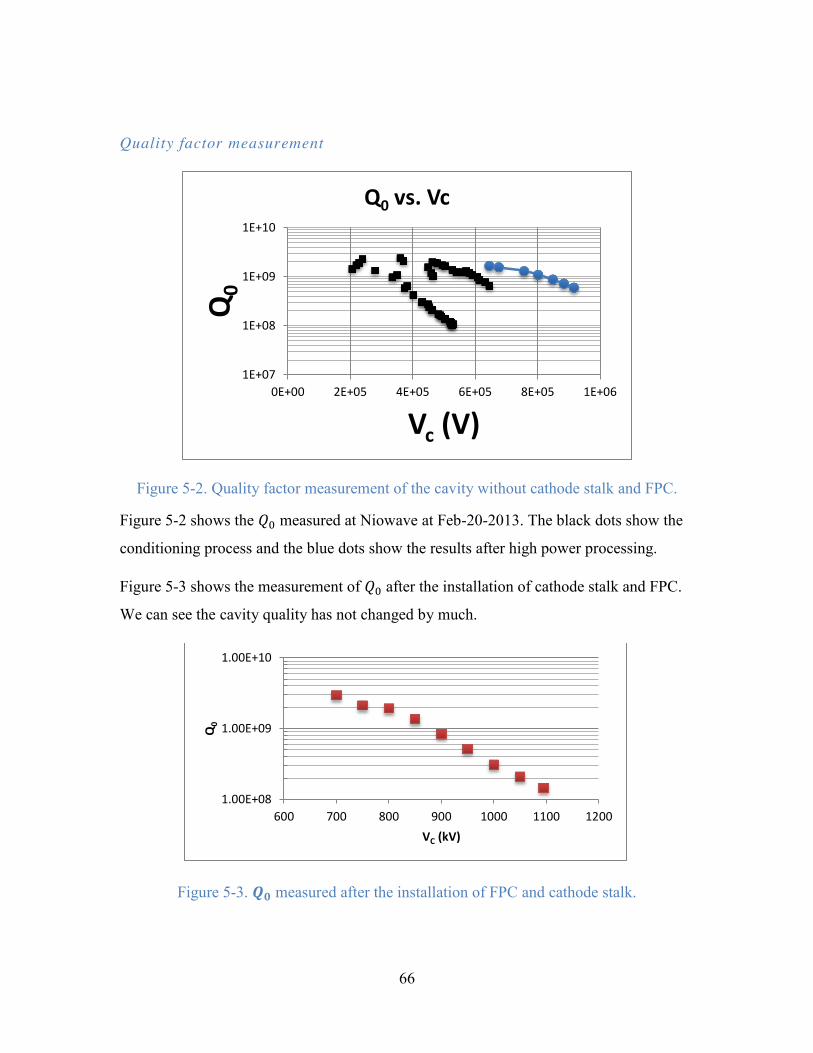
66
Quality factor measurement
Figure 5-2. Quality factor measurement of the cavity without cathode stalk and FPC.
Figure 5-2 shows the 𝑄 measured at Niowave at Feb-20-2013. The black dots show the
conditioning process and the blue dots show the results after high power processing.
Figure 5-3 shows the measurement of 𝑄 after the installation of cathode stalk and FPC.
We can see the cavity quality has not changed by much.
Figure 5-3. 𝑸𝟎 measured after the installation of FPC and cathode stalk.
1E+07
1E+08
1E+09
1E+10
0E+00 2E+05 4E+05 6E+05 8E+05 1E+06
Q0
Vc (V)
Q0 vs. Vc
1.00E+08
1.00E+09
1.00E+10
600 700 800 900 1000 1100 1200
Q0
VC (kV)

67
Dark Current and Helium Processing
Figure 5-4. Image of field emitter from the cavity.
Once the gun is at voltage, we started looking for the electron beam from field emission
(also called “dark current”). After we saw the strong dark current, presumably from the
emission tips on the surface of the cavity or the cathode stalk (Figure 5-4) [89], we
performed helium processing to the cavity. First, we charge the cavity with helium to
1 × 10 Torr. Then we put RF power into the cavity in pulsed mode for half an hour or
longer as necessary to clear up the surface of the cavity from field emitting spots. The
visible emitters near the cathode stalk tip were removed after the helium processing.
Figure 5-5 shows the progress of helium processing. With higher gun voltage the
radiation level is decreasing which is a clear indication that the emission centers got
conditioned.

68
Figure 5-5. Upper plot shows the gun voltage near the end of helium processing, lower plot shows the radiation does decrease.
After the helium processing, the injector was able to operate in CW mode up to 1.7 MV
gun voltage in continuous mode and 1.8 MV in pulsed mode.
5.2 Photocurrent Measurement The cathode was driven by 532 nm green laser, which was introduced into the injector
through a laser port and an input mirror. The cathode puck is mirror finished, and the
reflectivity of the cathode area on this puck is more than 38%. A significant amount of
light reflects from the puck. Therefore, we have another mirror on the opposite location
of the input one to guide the reflected beam out of the injector system. Figure 5-6 shows
the section view of the cavity with laser cross, FPC, cathode and laser path.
During the first photoelectric current commissioning, we were able to establish CW
operation under 1.56 MV gun voltage. The photoemitted beam was observed on the
integrated current transformer (ICT) at the exit of the 112 MHz SRF gun.
mre
m/h
our

69
The initial bunch charge was space charge limited at 1.35 nC under 1.5mm FWHM laser
spot size.
Figure 5-6. The laser path (bright green lines) and details of FPC and cathode in 112 MHz injector [90].
The measured QE was 0.8% which agreed well with our expectation. We could clearly
see the space charge limitation on the bunch charge versus laser power plot in Figure 5-7.
After we had observed the saturation we increased the laser spot size to 2.5 mm FWHM
and generated 2.4 nC (3 nC in maximum) bunch charge as shown Figure 5-8[91]. While
operating the laser at a 5 kHz repetition-rate, we were able to generate an average beam
current above 15 µμA.

70
Figure 5-7. Measured charge dependency on laser energy under 1.56 MV gun voltage [91].

71
Figure 5-8. Raw and integrated ICT signal. The ICT calibration is 0.8 nC per 1 nV. The signal here corresponding to a 2.4 nC bunch charge [91].
The momentum of the beam is also measured by turning on the vertical trim dipole
magnet. The result of the vertical shift of the beam versus current in trim-D is shown in
Figure 5-9 which indicates the kinetic energy of electrons equal to 1.6 MeV.

72
Figure 5-9. Vertical shift of beam position at YAG 1 versus current in Trim D [91].
5.3 Summary The SRF commissioning of the injector was successful after several iterations. A number
of multipacting barriers predicted by our simulation were observed and eventually
overcome. The cavity was able to run in CW mode up to 1.7 MV gun voltage after
helium processing. Photoemission was successful, and we were able to extract a record 3
nC from single laser pulse with repetition rate 5 kHz. This essentially gives us 15 µμA
average current which is also a world record for an SRF photoinjector.
73
6 Alternative Cathode for the Gun: Diamond Amplifier The 112 MHz injector is also compatible with other types of photocathodes. Besides the
traditional metal or semiconductor cathodes, an interesting alternative is the diamond
amplifier. In this chapter we will discuss this relatively new type of cathode that was
developed at BNL [92, 93, 94].
6.1 Diamond as Secondary Electron Emitter The band gap of the CVD diamond we used for this experiment is 5.47 eV which means
the bottom of the conduction band is close to the vacuum level [95]. In this case, if we
produce a monolayer of hydrogen on the surface of the diamond and form a dipole layer,
the vacuum level will be lowered effectively to the point that is below the conduction
band on the surface, thus obtaining a negative electron affinity (NEA) surface [96]. When
an electron reaches the surface from inside of the diamond, it is very easy for it to escape
to the vacuum side.
The conceptual scheme of our experiment on diamond secondary emission in DC system
is shown in Figure 6-1. One face of the diamond is coated with 30 nm platinum, which
will serve as the electron injection electrode. The other surface of the diamond is
hydrogenated as describe in procedure first published in [93]. We use a 10 keV primary
electron beam to generate electron-hole (e-h) pairs near the surface of impact. A small
portion of the e-h pairs will recombine, and the rest will drift under the external electric
field towards opposite surface. The holes will recombine with the injected electron from
the platinum electrode [97]. The electrons will drift all the way across the bulk diamond
to the hydrogenated surface (we can ignore the small fraction that may be trapped by
impurities or defects in the diamond crystal). After the electrons reach the NEA surface,
some of the electrons will emit to the vacuum, and some will be trapped on the surface
[98]. The trapped electrons will form a shielding field inside the bulk diamond and
eventually shut down the drift process. To mitigate this trapping problem, we change the
DC high voltage bias to a pulsed signal while keeping the primary electron on all the time.
Thus, when the high voltage bias is off the shielding field will act as a drifting field for
the holes so that the holes will reach the NEA surface and neutralize the trapped electrons.

74
Figure 6-1. Schematic diagram of the diamond amplifier [98].
6.2 Diamond Amplifier for 112 MHz SRF Injector Instead of using DC bias as the driving field for the secondary electron we would like to
use the RF field because of its intrinsic advantages. First, the RF field could be much
stronger compared to the state of art DC field. . Another useful feature of the RF field is
the sinusoidal behavior in the time domain, which means that the electric field reverses
automatically. We can use this as the cleaning field for the neutralization process
discussed above.
For the test of the Diamond Amplifier in an SRF gun, we can use the same stalk that was
designed for the multi-alkali cathode. As for the source of primary electrons, we decided
to use a newly designed DC assembly with a UV-driven copper cathode. A CAD model
and a photo of this system are shown in Figure 6-2.
This is the first prototype Diamond Amplifier we made for testing in the SRF gun. There
are four major pieces. A gold plated copper top plate is used to hold the diamond and
ground it to the cavity. A ceramic spacer serves as an insulator between the grounded top
plate and biased molybdenum base. It also acts as a holder for the cathode, and defines
the crucial distance between the cathode and diamond. The third part is the
cathode/mirror pair that provides the electron beam and guides the laser beam out of the

75
cavity. The fourth part is the molybdenum base that works as the connection between the
Diamond Amplifier and the transport arm.
The laser enters the assembly through a hole in the top plate and illuminates the cathode.
There is an aluminum electrode surrounding the cathode, with a shape optimized for
focusing the electron beam. After the laser bounces off the mirror-finished cathode, it
hits a metal-coated mirror on the other side. This mirror then redirects the laser out of the
amplifier through an exit hole in the top plate. Figure 6-3 shows how the amplifier may
be positioned in the stalk and cavity as well as the paths of laser and electron beams. The
angles of the cathode and mirror are chosen so that the laser beam can escape the cavity
with no obstacles, and the electron beam can hit the center of the diamond so that we do
not have to worry about charging up of the ceramic spacers. The cathode bias is provided
by a -5 kV DC power supply. The top plate is grounded to the cavity through the gold
plated fingers.
Figure 6-2. Section view of the Diamond Amplifier: red lines show the path of UV light. Small insert is a photo of the first prototype Diamond Amplifier with a penny on the side as a size reference.

76
Figure 6-3. Laser path (red) and electron path (green) in the Amplifier and cavity.
To find the optimal orientation of the cathode, we used CST Particle Studio to simulate
the trajectory of electron beam after it leaves the cathode. Table 6-1 shows parameters we
used in the simulation.
Table 6-1. Parameters for simulation
Parameters Value
High Voltage -5 kV
Average Current 5 nA
Pulse width 1 nS
Repetition rate 80 kHz
After a few iterations, the angle between the normal direction of cathode and axis of the
cavity is chosen to be 42 degrees. The distance between centers of the cathode and the
diamond is optimized to 6.6 mm. Figure 6-4 shows the potential distribution inside the
amplifier and the electron beam trajectory. In tests, we were able to guide the primary
beam onto the center of Pt coating layer on the back of the diamond. The distance
between the center of the beam spot and the center of the diamond was eventually
brought down to 180 𝜇m. RF field leakage through the holes in the top plate was taken

77
into consideration, and we found that the field is low enough that there is no observable
effect on the beam energy and position.
We built a prototype Amplifier and made some preliminary measurement on it to
demonstrate the feasibility of our design regarding laser and electron beam paths.
Figure 6-4. Trajectory of electron beam between the primary cathode and diamond. Smaller picture shows the potential distribution inside the Amplifier.
Figure 6-5 shows the test with a green alignment laser. The incoming laser beam passes
through a partially reflecting Kapton film window, and then illuminates the copper
cathode. After two reflections it comes out of the exit hole on the other side of the top
plate. The reflected laser beam from the Kapton window is indicated as a weaker spot.

78
Figure 6-5. Demonstration of the laser beam passage[99].
We also measured the percentage of electrons that we were able to capture with a dummy
electrode, which is acting in place of diamond. In this measurement, we successfully
applied -5 kV bias to the cathode. Then a 220 nm UV light generated by a deuterium
lamp and a monochromator was introduced to the amplifier.
We recorded the current leaving the cathode and the current intercepted by an isolated
dummy electrode under different bias voltages. The result of the measurement is shown
in Figure 6-6.

79
Figure 6-6. Percentage of electrons reaching dummy electrode over electrons leaving cathode.
One can see that about half of the electrons that left the primary cathode did not make it
to the dummy electrode. This can be the result of stray light illuminating the cone-shaped
electrode sitting on top of the cathode. Since the spot size of UV light from lamp could
not be reduced to match exactly the size of the copper cathode, we expect a certain
amount of electrons from the aluminum electrode.
Considering the total area of the electrode and the QE of the aluminum, it is possible that
nearly half of the signal corresponding to the current leaving cathode was due to the
photoemission from aluminum. In future tests, the light source will be changed to a UV
laser and the size of the light spot will be sufficiently reduced to minimize the number of
electrons caused by stray light.
In future work, we are planning to modify the previous one hundred percent coverage
metal coating to a lithographically patterned grid coating. Because the metal layer will
reduce the energy of primary electrons, less coverage means larger effective impact
energy from primary beam. Hence, the total number of secondary electron product in
each pulse will be increased accordingly. The tradeoff is that the weaker electric field
established by grid coating inside diamond will drag less secondary electrons to the
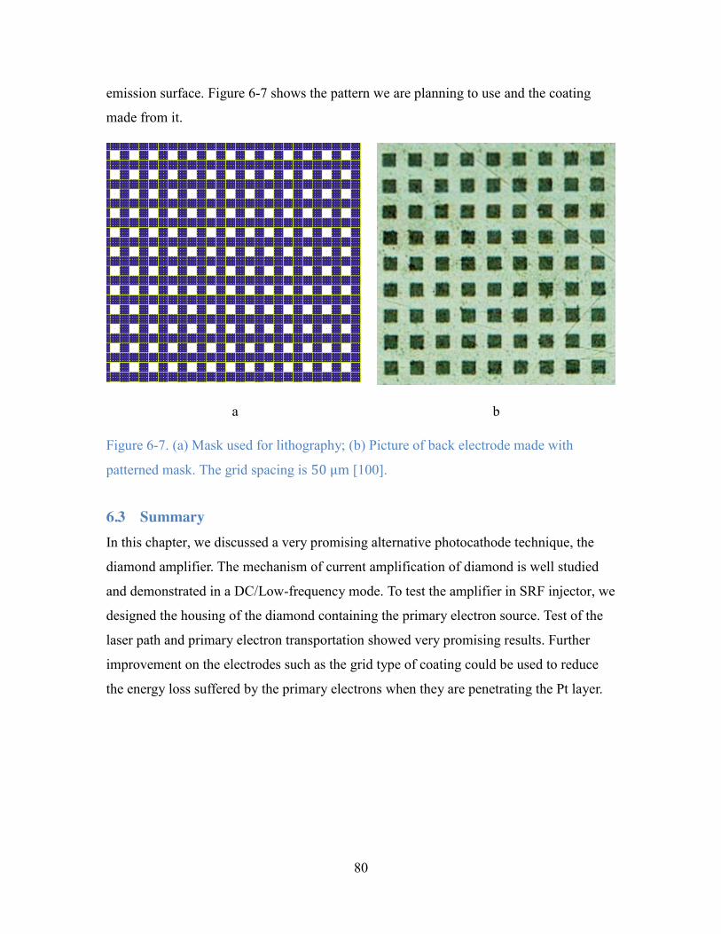
80
emission surface. Figure 6-7 shows the pattern we are planning to use and the coating
made from it.
a b
Figure 6-7. (a) Mask used for lithography; (b) Picture of back electrode made with
patterned mask. The grid spacing is 50 µμm [100].
6.3 Summary In this chapter, we discussed a very promising alternative photocathode technique, the
diamond amplifier. The mechanism of current amplification of diamond is well studied
and demonstrated in a DC/Low-frequency mode. To test the amplifier in SRF injector, we
designed the housing of the diamond containing the primary electron source. Test of the
laser path and primary electron transportation showed very promising results. Further
improvement on the electrodes such as the grid type of coating could be used to reduce
the energy loss suffered by the primary electrons when they are penetrating the Pt layer.

81
7 Conclusion We have presented the design, fabrication, and commissioning of a high-bunch-charge
SRF photoemission electron source based on an 112 MHz quarter-wave resonator. The
112 MHz SRF cavity was originally designed for the electron cooling project at BNL and
eventually modified to serve as the injector of the Coherent electron Cooling Proof-of-
Principle (CeC PoP) project.
The major part of RF design of the cavity was done in previous work. Here we discussed
the complementary work for the cavity design including the Lorentz detuning,
mechanical detuning sensitivity, and multipacting behavior study. A GPU accelerated C
code was written to simulate the multipacting phenomenon in the RF structures such as
the cavity, couplers, and waveguides. The code has excellent transferability and can be
easily modified to accommodate other similar problems such as the dark current tracking
and field emission simulation. By parallelizing the most time-consuming part of the
particle tracking algorithm, the coordinates updating and particle locating functions, the
GPU code runs on a Nvidia Tesla k40 can give a roughly five times performance boost
comparing to the CPU version of the same function running on an Intel i7 4795.
We designed a coaxial fundamental power coupler so that it is compatible with the
existing cryomodule and capable of providing up to 780 W beam power with enough
safety margins. The coaxial coupler has the advantage of large coupling factor, a
sufficient fine-tuning range and minimum dipole kick to the beam. The large coupling
range gives us more edge when we need to power through the tough multipacting barriers.
Moreover, it potentially allows us to provide more beam power to higher bunch charge
beams. Less dipole kick is helpful for reducing the emittance growth. However, the
coaxial coupler also has a disadvantage of higher susceptibility to multipacting between
the inner and outer conductors. Fortunately, we were able to simulate the MP in the FPC
and find the way of mitigating the problem by coating the surface of the inner conductor
with gold.
The gun employs high QE multi-alkali (K2CsSb) photocathodes deposited on small
molybdenum pucks. The recipe of cathode deposition has been well developed and
adopted by the cathode fabrication group at BNL. We can routinely grow cathodes with

82
QE better than 5% in the deposition chamber located at the Instrumentation Department
at BNL. The cathode preservation requires high vacuum condition, ideally better than
1 × 10 Torr. Hence, we designed and built a cathode transport system (nickname
‘garage’) that can take up to three cathodes from the deposition chamber to the 112 MHz
injector in the RHIC tunnel while keeping the vacuum under 1 × 10 Torr. We also
presented the design and test result of a half-wavelength choke structure cathode stalk.
The stalk allows the cathode to operate at room temperature so that the QE at the
wavelength of 532 nm can be preserved. It also minimizes the voltage drop between the
cathode and the cavity because of the choke structure. An impedance mismatch was
introduced to the cathode stalk to further minimize the impedance of the choke structure
seem by the cavity and consequently reduce the voltage drop in the cathode-cavity gap.
Multipacting is an issue of this design, as expected, and we reduced the multiplication of
secondary electrons by coating the stalk with gold. This coating also reduces the
emissivity of the surface hence reduces the thermal load from radiation to the cryosystem.
Simulation results show promising improvement by this surface treatment. However,
according to the experimental observation, the multipacting inside the stalk structure still
needs excessive conditioning time as compared to the FPC. Further improvement of this
issue can be achieved by coating the surface with TiN.
The SRF injector was installed in the RHIC tunnel as part of the CeC PoP experiment. To
find the optimum parameters of operation, the author wrote a python script that
implements a genetic algorithm to search for the parameter vector that gives the best
beam quality. According to the beam dynamics simulation, the injector should be able to
provide a beam with emittance around 7.25 mm-mrad and energy spread better than 0.5%.
During the first round of commissioning, we managed to overcome multipacting and
field emission to a level allowing demonstrating first beam with bunch charge of 3 nC at
5 kHz repetition rate which is the record in such devices.
An alternative cathode, Diamond Amplifier, was also studied intensively. The compatible
parts of the amplifier were designed and tested outside the SRF cavity. The result of the
preliminary test is promising, and future test in the SRF injector should provide more
interesting result.

83
References: 1 Z. Huang, K. Kim, A Review of X-ray Free-Electron Laser Theory, ANL-AAI-PUB-2007-002, December 2006. 2 I. Ben-Zvi, L. Ahren, et al., Electron Cooling for RHIC, 2nd EIC workshop, Jefferson Lab, 2004. 3 A. V. Fedotov, I. Ben-Zvi, et al., High-energy electron cooling in a collider, New Journal of Physics 8
283, 2006. 4 J. Smedley, T. Rao, E. Wang, K2CsSb Cathode Development, AIP Conf. Proceedings of 18th Int’l. Spin Physics Symp., 1062-1066, 2009. 5 S. Belomestnykh, I. Ben-Zvi1, et al., Design and First Cold Test of BNL Superconducting 112 MHz QWR for Electron Gun Applications, Proceedings PAC2011, New York, NY, USA, 2011. 6 T. L. Grimm, C. Boulware, et al., Development of a Low Frequency Superconducting RF Electron Gun, DOE-NP SBIR Final Scientific Report, DE-FG02-07ER84861. 7 T. Xin, S. Belomestnykh, et al., Design of the Fundamental Power Coupler and Photocathode Inserts for the 112 MHz Superconducting Electron Gun, Proceeding of SRF2011, Chicago, IL, USA, 2011. 8 https://confluence.slac.stanford.edu/display/AdvComp/ACE3P+-+Advanced+Computational+Electromagnetic+Simulation+Suite. 9 E. Wang, Characterization of Multi-alkali Antimonide Cathodes at Cryogenic Temperature and its Performance in SRF Gun, Proceeding of Workshop on Energy Recovery Linacs 2015, Stony Brook University, Stony Brook, NY, USA, 2015. 10 C. G. Montgomery, R. H. Dicke, E. M. Purcell, Principles of Microwave Circuits, IET, 1948, ISBN 0863411002, 9780863411007. 11 T. Vecchione, I. Ben-Zvi, D. H. Dowell, et al., A Low Emittance and High Efficiency Visible Light Photocathode for High Brightness Accelerator-based X-ray Light Sources, Applied Physics Letters 99(3):4103-3, 2011. 12 http://www.desy.de/~mpyflo/. 13 T. Xin, S. Belomestnykh, et al., Diamond Amplifier Design and Preliminary Test Results, Proceeding of NAPAC 2013, Pasadena, CA, USA, 2013. 14 B. M. Dunham, C. K. Sinclair, I. V. Bazarov, Performance of a very High Voltage Photoemission Electron Gun for a High Brightness, High Average Current ERL Injector. Proceeding of PAC07, Albuquerque, New Mexico, USA, 2007. 15 F. Loehl, I. Bazarov, S. Belomestnykh, et al., High Current and High Brightness Electron Sources, Proceeding of IPAC’10, Kyoto, Japan, 2010. 16 D. Proch, Superconducting Cavities for Accelerators, Rep. Prog. Phys. 61 431-482, 1998. 17 Hasan Padamsee, RF Superconductivity for Accelerators, John Wiley & Sons INC, ISBN 0-471-15423-6. 18 Y. Koshiba, T. Aoki, K. Sakaue, et al., Development of an RF Electron Gun for Ultra-short Bunch Generation, Proceeding of IPAC12, New Orleans, Louisiana, USA, 2012. 19 B. Aune, R. Bandelmann, D. Bloess, et al., The Superconducting TESLA Cavities, arXiv:physics/0003011v1 [physics.acc-ph]. 20 J. F. Schmerge, A. Brachmann, D. Dowell, et al., The LCLS-II Injector Design, Proceeding of FEL14, Basel, Switzerland, 2014. 21 E. Jensen, RF Cavity Design, CERN Accelerator School, Chios, 2011. 22 J. D. Jackson, Classical Electrodynamics, Third Edition, ISBN 0-471-30932-X. 23 F. Gerigk, Cavity Types, CAS, RF for Accelerators, Ebeltoft, Denmark, 2010. 24 I. Ben-Zvi and J.M. Brennan, The Quarter Wave Resonator as a Superconducting LINAC Element, Nuclear Instruments and Methods in Physics Research, A212, 73, 1983. 25 J.M. Brennan, B. Kurup, I. Ben-Zvi, J.S. Sokolowski, Performance Test of a Superconducting Quarter Wave Resonator, Nuclear Instruments and Methods in Physics Research, A242, 23, 1985. 26 D. M. Pozar, Microwave Engineering, fourth edition, John Wiley & Sons INC, ISBN 978-0-470-63155-3. 27 I. Ben-Zvi, Quarter Wave Resonators for beta~1 Accelerators, Proceeding of SRF 2011, Chicago, Illinois, USA, 2011. 28 http://laacg.lanl.gov/laacg/services/download_sf.phtml. 29 X. Chang, Optimization of the BNL-Niowave 112MHz SRF cavity, BNL internal report. 30 Hasan Padamsee, RF Superconductivity for Accelerators, John Wiley & Sons INC, ISBN 0-471-15423-6.

84
31 J.R. Delayen, Longitudinal Transit Time Factors of Short Independently-Phased Accelerating Structures for Low Velocity Ions, Nuclear Instruments and Methods in Physics Research, A258, 15-25, 1987. 32 R. Parodi, Multipacting, https://arxiv.org/ftp/arxiv/papers/1112/1112.2176.pdf. 33 D. Naik, I. Ben-Zvi, Multipacting Simulation Study for 56 MHz Quarter Wave Resonator using 2D Code, http://www.c-ad.bnl.gov/ardd/ecooling/docs/PDF/56_MHz/ap_note_343%20(2).pdf. 34 J. Tuckmantel , One Point Multipacting Levels Determined without Electron Tracking, Proceedings of the Fourth Workshop on RF Superconductivity, KEK, Tsukuba, Japan, 1989. 35 Z. Zheng, A. Facco, et al., Multipacting Suppression Modeling for Half Wave Resonator and RF Coupler, Proceedings of LINAC2012, Tel-Aviv, Israel, 2012. 36 R. Udiljak, D. Anderson, et al., Multipactor in a coaxial transmission line. I. Analytical study, Physics of Plasmas 14, 033508 S2007d, 2007. 37 R. Udiljak, Multipactor in Low Pressure Gas and in Nonuniform RF Field Structures, Thesis for the degree of Doctor of Philosophy, Department of Radio and Space Science, Chalmers University of Technology, Göteborg, Sweden, 2007. 38 I. Ben-Zvi, J.F. Crawford and J.P. Turneaure, Electron Multiplication in Cavities. IEEE Trans. Nucl. Sci. NS 20, 8, 54, 1973. 39 R. L. Geng, Multipacting Simulations for Superconducting Cavities and RF Coupler Waveguides, Proceeding of PAC2003, Portland, Oregon, USA, 2003. 40 M. Furman, M. Pivi, Probabilistic Model for the Simulation of Secondary Electron Emission, Phys. Rev. ST Accel. Beams 5, 2002. 41 http://www-mhf.desy.de/~brinkma/multipac/neu2_multipac.pdf. 42 http://www.jlab.org/~genfa/fishpact/. 43 https://confluence.slac.stanford.edu/display/AdvComp/ACE3P+-+Advanced+Computational+Electromagnetic+Simulation+Suite. 44 CST Microwave Studio® https://www.cst.com/products/CSTMWS. 45 http://www.nersc.gov/. 46 M. Houston, General Purpose Computation on Graphics Processors (GPGPU), https://graphics.stanford.edu/~mhouston/public_talks/R520-mhouston.pdf. 47 https://www.udacity.com/course/intro-to-parallel-programming--cs344. 48 https://www.coursera.org/course/hetero. 49 http://docs.nvidia.com/cuda/cuda-c-programming-guide. 50 L. H. Lyu, Numerical Simulation of Space Plasmas (I), http://www.ss.ncu.edu.tw/~lyu/lecture_files_en/lyu_NSSP_Notes/lyu_NSSP_Content.html. 51 A. Haselbacher, F.M. Najjar and J.P. Ferry, An Efficient and Robust Particle-Localization Algorithm for Unstructured Grids, Journal of Computational Physics vol. 225 (2) p. 2198-2213, 2007. 52 T. Xin, I. Ben-Zvi, et al., A GPU based 3D Particle Tracking Code for Multipacting Simulation, Proceeding of SRF 2015, Whistler, Canada, 2015. 53 C. J. Bradley, The Algebra of Geometry: Cartesian, Areal and Projective Co-ordinates. Bath: Highperception. ISBN 978-1-906338-00-8. 54 S. Belomestnykh, I. Ben-Zvi, et al., Superconducting 112 MHz QWR Electron Gun, Proceeding of SRF2011, Chicago, Illinois, USA, 2011. 55 T. Roser, RHIC Status and Requirements, http://www.iaea.org/inis/collection/NCLCollectionStore/_Public/33/004/33004474.pdf. 56 T. L. Grimm, C. H. Boulware, et al., Development of a Low Frequency Superconducting RF Electron Gun, SBIR II report, 2011. 57 A. Kumar, A. R. Jana and V. Kumar, A Study of Dynamic Lorentz Force Detuning of 650 MHz β= 0.9 Superconducting Radiofrequency Cavity, Nuclear Instruments and Methods in Physics Research, Section A: Accelerators, Spectrometers, Detectors and Associated Equipment vol. 750 p. 69-77, 2013. 58 J. R. Harris et al., Design and operation of a superconducting quarter-wave electron gun, Phys. Rev. ST Accel. Beams 14, 053501, 2011. 59 F. Reif, Fundamental of Statistical and Thermal Physics, McGraw Hill Higher Education, ISBN-10: 1577666127. 60 http://www.engineeringtoolbox.com/emissivity-coefficients-d_447.html. 61 L. Cultrera, S. Karkare, et al., Cold Electron Beams From Cryo-cooled, Alkali Antimonide Photocathodes, arXiv:1504.05920 [physics.acc-ph].

85
62 E. Wang, Characterization of Multi-alkali Antimonide Cathodes at Cryogenic Temperature and its Performance in SRF Gun, Proceeding of Workshop on Energy Recovery Linacs 2015, Stony Brook University, Stony Brook, NY, USA, 2015, http://accelconf.web.cern.ch/AccelConf/ERL2015/talks/tuiclh1027_talk.pdf. 63 E. Wang, T. Rao, and I. Ben-Zvi, Enhancement of Photoemission and Post Processing of K2CsSb Photocathode using Excimer Laser, Phys. Rev. ST Accel. Beams 17, 023402, 2014. 64 T. Vecchione, J. Feng, W. Wan, et al., Effect of Roughness on Emittance of Potassium Cesium Antimonide Photocathode, Proceeding of IPAC2012, New Orlean, Louisiana, USA, 2012. 65 D. J. Bradley, M.B. Allenson, and B.R. Holeman, The Transverse Energy of Electrons Emitted from Photocathode, Journal of Physics D: Applied Physics, 1977. 10(1): p. 111. 66 D. Xiang, W. H. Huang, et al., First Principle Measurements of Thermal Emittance for Copper and Magnesium, Proceeding of PAC07, Albuquerque, New Mexica, USA, 2007. 67 H. J. Qiang, C. Li, et al., Experimental Investigatino of Thermal Emittance components of Copper Photocathode, Phys. Rev. ST Accel. Beams 15(4): p. 040102, 2012. 68 H. Xie, E. Wang, et al., Characterizatio of Multi-alkali Photocathode at Cryogenic Temperature, to be submitted. 69 G. Wang, V. N. Litvinenko, M. Blaskiewicz, Energy Modulation in Coherent Electron Cooling, Proceeding of IPAC2013, Shanghai, China, 2013. 70 G. Wang, Y. Hao, V.N. Litvinenko, Influence of Electron Beam Parameters on Coherent Electron Cooling, Proceeding of IPAC2012, New Orlean, Louisiana, USA, 2012. 71 S. Y. Lee, Accelerator Physics, World Scientific, ISBN: 978-981-4374-94-1. 72 P. W. Milonni, J. H. Eberly, Laser Physics, Wiley, ISBN: 978-0-470-38771-9. 73 D. Nguyen, S. Russell, N. Moody, Theory and Practice of Free-Electron Lasers, Lecture Note of USPAS 2009, University of New Mexico, Albuquerque, NM, USA, 2009, http://uspas.fnal.gov/materials/09UNM/Day%201.pdf. 74 F. Sannibale, D. Filippetto, C. Papadopoulos, Electron Injector for 4th Generation Light Sources, USPAS 2012, http://controls.als.lbl.gov/als_physics/Fernando/USPASJan2012/Lectures/. 75 W. F. Krolikowski, W. E. Spicer, Photoemission Studies of the Noble Metals. I. Copper, Phys. Rev. 185 882, 1969. 76 M. Cardona, L. Ley, Photoemission in Solids I, Springer-Verlag, 1978, ISBN: 978-3-540-08685-7. 77 David Dowell, Electron Injectors for 4th Generation Light Sources, USPAS, 2010. 78 W.K.H. Panofsky and W.A. Wenzel, Rev. Sci. Instrum., 27, 967, 1956. 79 M. Reiser, Theory and Design of Charged Particle Beams, Wiley, ISBN: 9780471306160. 80 T. P. Wangler, Space-Charge-Induced Emittance Growth in an Elliptical Charged Particle Beam with a Parabolic Density Distribution. Proceeding of PAC1993, Washington, DC, USA, 1993. 81 J. B. Rosenzweig and L. Serafini, Transverse Particle Motion in Radio-frequency Linear Accelerators, Phys. Rev. E 49, 1599,1994. 82 C. A. Coello, G. B. Lamont, Application of Multi-Objective Evolutionary Algorithms, World Scientific, ISBN: 981-256-106-4. 83 I. V. Bazarov, C. K. Sinclair, Multivariate Optimization of a High Brightness DC Gun Photoinjector, Phys. Rev. ST Accel. Beams 8, 034202, 2005. 84 K. Deb, A. Pratop, S. Agarwal, et al., A Fast and Elitist Multiobjective Genetic Algorithm: NSGA-II, Transactions on Evolutionary Computation, 6. 2, 2002. 85 A. Konak, D. W. Coit, A. E. Smith, Multi-Objective Optimization Using Genetic Algorithms: A Tutorial, Reliability Engineering & System Safety vol. 91 (9) p. 992-1007, 2006. 86 K. Miettinen, Nonlinear Multiobjective Optimization, Springer, ISBN: 978-0-7923-8278-2. 87 J. Tuozzolo, CeC Engineering, C-AD ASSRC Review, http://www.c-ad.bnl.gov/ardd/ASSRC%20CeC%20PoP/Presentations/CeC%20PoP%20Engineering%20Introduction.pdf. 88 S. Belomestnykh, I. Ben-Zvi, et al., Commissioning of the 112 MHz SRF gun and 500 MHz Bunching Cavities for the CeC PoP LINAC, https://www.bnl.gov/isd/documents/88864.pdf. 89 S. Belomestnykh, I. Ben-Zvi, et al., Commissioning of 112 MHz SRF Gun, Proceeding of SRF2015, Whistler, Canada, 2015. 90 Courtesy of John Skaritka. 91 I. Pinayev, V. N. Litvinenko, et al., High-gradient High-charge CW Superconducting RF gun with K2CsSb Photocathode, arXiv:1511.05595v1 [physics.acc-ph].

86
92 E. Wang, X. Chang, et al., Systematic Study of Hydrogenation in a Diamond Amplifier, Phys. Rev. ST Accel. Beams 14, 061302, 2011. 93 X. Chang, I. Ben-Zvi, et al., Electron Beam Emission from a Diamond-Amplifier Cathode, Phys. Rev. Lett. 105, 164801, 2010. 94 E. Wang, X. Chang, et al., Secondary-electron Emission from Hydrogen-Terminated Diamond: Experiments and model, Phys. Rev. ST Accel. Beams 14, 111301, 2011. 95 J. vad der Weide, Z. Zhang, et al., Negative-electron-affinity Effects on the Diamond (100) Surface, Phys. Rev. B., 50 8, 1994. 96 A. K. Tiwari, J. P. Goss, et al., Electronic and Structural Properties of Diamond (001) Surfaces Terminated by Selected Transition Metals, Phys. Rev. B., 86, 155301, 2012. 97 M. Gaowei, E. M. Muller, et al., Annealing Dependence of Diamond-metal Schottky Barrier Height Probed by Hard X-ray Photoelectron Spectroscopy, Appl. Phys. Lett. 100, 201606, 2012. 98 X. Chang, I. Ben-Zvi, et al., Neutralizing Trapped Electrons on the Hydrogenated Surface of a Diamond Amplifier, Phys. Rev. ST Accel. Beams 15, 013501, 2012. 99 Courtesy of Erdong Wang. 100 Courtesy of Mengjia Gaowei.