tlc5954 48-channel, constant-current led driver with
TRANSCRIPT

BLANK Signal
Data Latch
Shift Clock
VLED
Input Serial Data SIN
SCLK
LAT
BLANK
SOUT
VCC
GND
OUTR0 OUTB15
TLC5954
GND
VCC
GND
GND
x48
Output Serial Data
+
PowerPAD
Product
Folder
Sample &Buy
Technical
Documents
Tools &
Software
Support &Community
TLC5954SBVS241 –APRIL 2014
TLC5954 48-Channel, Constant-Current LED Driver with Global Brightness Control,LED Open-Short Detection, and Power-Save Mode
1 Features 2 Applications1• 48 Constant-Current Sink Output Channels with • LED Video Displays
On or Off Control • Variable Message Signs (VMS)• Current Capability: • Illumination
– 34.9 mA for 32 Channels3 Description– 24.4 mA 16 ChannelsThe TLC5954 is a 48-channel, constant-current sink• No External Resistor for Current SettingLED driver. Each channel can be turned on or off by
• Maximum Current Control (MC): 3 Bits (8 Steps) writing data to an internal register. The output• Global Brightness Control (BC) for Each Color channels (OUTXn) are grouped into three groups of
16 channels. Each channel group (R, G, and B) has aGroup: 7 Bits (128 Steps), Three Groups128-step global brightness control (BC) function. The• LED Power-Supply Voltage: Up to 10 Vmaximum current value of all 48 channels can be set• VCC = 3.0 V to 3.6 V with an 8-step maximum current control (MC)
• Constant-Current Accuracy: function. The device has two error flags: LED opendetection (LOD) and LED short detection (LSD). The– Channel-to-Channel = ±1% (typ), ±3% (max)error flags can be read via a serial interface port. The– Device-to-Device = ±2% (typ), ±4% (max) device also has a power-save mode that sets the
• Data Transfer Rate: 30 MHz total current consumption to 7 µA (typ) when alloutputs are off.• BLANK Pulse Duration: 40 ns (min)
• LED Open Detection (LOD) Device Information(1)• LED Short Detection (LSD)
DEVICE NAME PACKAGE BODY SIZE• Power-Save Mode (PSM): 7-µA Consumption, TLC5954 VQFN (56) 8 mm × 8 mm
High-Speed Recovery(1) For all available packages, see the orderable addendum at• Undervoltage Lockout Sets Default Data the end of the datasheet.
• Delayed Switching Minimizes Inrush Current space• Operating Temperature: –40°C to +85°C
space
space
space
Application Circuit
1
An IMPORTANT NOTICE at the end of this data sheet addresses availability, warranty, changes, use in safety-critical applications,intellectual property matters and other important disclaimers. PRODUCTION DATA.

TLC5954SBVS241 –APRIL 2014 www.ti.com
Table of Contents8.1 Overview ................................................................. 161 Features .................................................................. 18.2 Functional Block Diagram ....................................... 172 Applications ........................................................... 18.3 Feature Description ................................................ 183 Description ............................................................. 18.4 Device Functional Modes........................................ 234 Revision History..................................................... 28.5 Register Maps ......................................................... 275 Pin Configuration and Functions ......................... 3
9 Applications and Implementation ...................... 336 Specifications......................................................... 49.1 Application Information............................................ 336.1 Absolute Maximum Ratings ...................................... 49.2 Typical Application .................................................. 336.2 Handling Ratings....................................................... 5
10 Power Supply Recommendations ..................... 366.3 Recommended Operating Conditions....................... 511 Layout................................................................... 366.4 Thermal Information .................................................. 6
11.1 Layout Guidelines ................................................. 366.5 Electrical Characteristics........................................... 611.2 Layout Example .................................................... 376.6 Switching Characteristics .......................................... 7
12 Device and Documentation Support ................. 386.7 Typical Characteristics .............................................. 812.1 Device Support...................................................... 387 Parameter Measurement Information ................ 1112.2 Documentation Support ........................................ 387.1 Pin Equivalent Input and Output Schematic12.3 Trademarks ........................................................... 38Diagrams.................................................................. 1112.4 Electrostatic Discharge Caution............................ 387.2 Test Circuits ............................................................ 1112.5 Glossary ................................................................ 387.3 Timing Diagrams..................................................... 12
13 Mechanical, Packaging, and Orderable8 Detailed Description ............................................ 16Information ........................................................... 38
4 Revision History
Date Revision NotesApril 2014 * Initial release.
2 Submit Documentation Feedback Copyright © 2014, Texas Instruments Incorporated
Product Folder Links: TLC5954

Thermal Pad(Solder Side, GND Terminal)
15
42
41
40
39
38
37
56
SOUT
OUTB9
OUTG9
OUTR9
OUTB8
OUTG8
OUTR8
OUTB7
OUTG7
OUTR7
OUTB6
OUTG6
OUTR6
BLANK
GN
D
OU
TB
13
OU
TG
13
OU
TR
13
OU
TB
12
OU
TG
12
OU
TR
12
OU
TB
11
OU
TG
11
OU
TR
11
OU
TB
10
OU
TG
10
OU
TR
10
VC
C
OU
TG
2
OU
TB
2
OU
TR
3
OU
TG
3
OU
TB
3
OU
TR
4
OU
TG
4
OU
TB
4
OU
TR
5
OU
TG
5
OU
TB
5
SIN
LA
T
SC
LK
GND
OUTR14
OUTG14
OUTB14
OUTR15
OUTG15
OUTB15
OUTR0
OUTG0
OUTB0
OUTR1
OUTG1
OUTB1
OUTR2
36
35
34
33
32
31
30
29
1
2
3
4
5
6
7
8
9
10
11
12
13
14
16
55
17
54
18
53
19
52
20
51
21
50
22
49
23
48
24
47
25
46
26
45
27
44
28
43
TLC5954www.ti.com SBVS241 –APRIL 2014
5 Pin Configuration and Functions
RTQ PackageVQFN-56
(Top View)
Copyright © 2014, Texas Instruments Incorporated Submit Documentation Feedback 3
Product Folder Links: TLC5954

TLC5954SBVS241 –APRIL 2014 www.ti.com
Pin FunctionsPIN
NAME NO. I/O DESCRIPTION
GND 1, 56 — Ground. All GND pins are connected internally.
Red LED constant-current outputs (OUTRn).2, 5, 8, 11, 14, 17, 20,OUTR0 to Multiple outputs can be tied together to increase the constant-current capability. Different voltages can be23, 30, 33, 36, 39, 44, OOUTR15 applied to each output. These outputs are turned on or off by the BLANK signal and the data in the output on47, 50, 53 or off control data latch.
Green LED constant-current outputs (OUTGn).3, 6, 9, 12, 15, 18, 21,OUTG0 to Multiple outputs can be tied together to increase the constant-current capability. Different voltages can be24, 31, 34, 37, 40, 45, OOUTG15 applied to each output. These outputs are turned on or off by the BLANK signal and the data in the output on48, 51, 54 or off control data latch.
Blue LED constant-current outputs (OUTBn).4, 7, 10, 13, 16, 19, 22,OUTB0 to Multiple outputs can be tied together to increase the constant-current capability. Different voltages can be25, 32, 35, 38, 41, 46, OOUTB15 applied to each output. These outputs are turned on or off by the BLANK signal and the data in the output on49, 52, 55 or off control data latch.
Serial data input of the 49-bit common shift register, Schmitt buffer input.When SIN is high, the LSB is set to 1 for only one SCLK input rising edge. If two SCLK rising edges are inputSIN 26 I while SIN is high, then the 49-bit shift register LSB and LSB+1 are set to 1. When SIN is low, the LSB is set to0 at the SCLK input rising edge.
Edge-triggered latch, Schmitt buffer input.The LAT rising edge latches data from the common shift register either into the output on or off data latch orthe maximum current control (MC), brightness control (BC), or function control (FC) data latch. When theLAT 27 I common shift register data are latched into the on or off data latch, data in the common shift register aresimultaneously replaced with SID, which is selected by SIDLD. Refer to the Output On or Off Data Latch andStatus Information Data (SID) sections for more details.
Serial data shift clock, Schmitt buffer input.Data present on SIN are shifted to the 49-bit common shift register LSB with the SCLK rising edge. Data in theSCLK 28 I shift register are shifted towards the MSB at each SCLK rising edge. The common shift register MSB appearson SOUT.
Blank all outputs, Schmitt buffer input.BLANK 29 I When BLANK is high, all constant-current outputs (OUTXn) are forced off. When BLANK is low, all OUTXn are
controlled by the on or off control data in the data latch.
Serial data output of the 49-bit common shift register.SOUT 42 O SOUT is connected to the MSB of the register. Data are clocked out at the SCLK rising edge.
VCC 43 — Power-supply voltage
Thermal pad — Ground. The thermal pad must be connected to GND on the printed circuit board (PCB).
6 Specifications
6.1 Absolute Maximum Ratingsover operating free-air temperature range (unless otherwise noted) (1)
MIN MAX UNITVCC Supply voltage (2) –0.3 4.0 VVIN Input voltage range SIN, SCLK, LAT, BLANK –0.3 VCC + 0.3 V
SOUT –0.3 VCC + 0.3 VVOUT Output voltage range OUTR0 to OUTR15, OUTG0 to OUTG15, –0.3 11 VOUTB0 to OUTB15TJ (max) Operating junction temperature 150 °C
(1) Stresses beyond those listed under Absolute Maximum Ratings may cause permanent damage to the device. These are stress ratingsonly, and functional operation of the device at these or any other conditions beyond those indicated under Recommended OperatingConditions is not implied. Exposure to absolute-maximum-rated conditions for extended periods my affect device reliability.
(2) All voltages are with respect to device ground pin.
4 Submit Documentation Feedback Copyright © 2014, Texas Instruments Incorporated
Product Folder Links: TLC5954

TLC5954www.ti.com SBVS241 –APRIL 2014
6.2 Handling RatingsMIN MAX UNIT
Tstg Storage temperature range –55 150 °CHuman body model (HBM), per ANSI/ESDA/JEDEC JS-001, all –200 2000 Vpins (1)
V(ESD) Electrostatic dischargeCharged device model (CDM), per JEDEC specification –500 500 VJESD22-C101, all pins (2)
(1) JEDEC document JEP155 states that 500-V HBM allows safe manufacturing with a standard ESD control process.(2) JEDEC document JEP157 states that 250-V CDM allows safe manufacturing with a standard ESD control process.
6.3 Recommended Operating ConditionsAt TA= –40°C to +85°C, unless otherwise noted.
PARAMETER TEST CONDITIONS MIN NOM MAX UNITDC CHARACTERISTICS (VCC = 3 V to 3.6 V)VCC Supply voltage 3.0 3.6 V
OUTR0 to OUTR15, OUTG0 toVO Voltage applied to output 10 VOUTG15, OUTB0 to OUTB15VIH High-level input voltage SIN, SCLK, LAT, BLANK 0.7 × VCC VCC VVIL Low-level input voltage SIN, SCLK, LAT, BLANK GND 0.3 × VCC VIOH High-level output current SOUT –2 mAIOL Low-level output current SOUT 2 mA
Operating free-air temperatureTA –40 +85 °CrangeOperating junction temperatureTJ –40 +125 °Crange
AC CHARACTERISTICS (VCC = 3 V to 3.6 V)fCLK (SCLK) Data shift clock frequency SCLK 30 MHztWH0 SCLK 10 nstWL0 SCLK 10 nstWH1 Pulse duration LAT 15 nstWH2 BLANK 60 nstWL2 BLANK 40 nstSU0 SIN to SCLK↑ 4 nstSU1 LAT↓ to SCLK↑ 20 ns
SCLK↑ resumes normal mode,tSU2 12 µsSetup time BLANK↓, PSMODE bit = 01bLAT↑ for all data latching except all
tSU3 0s resumes normal mode, BLANK↓, 12 µsPSMODE bit = 10b
tH0 SCLK↑ to SIN 3 nsHold time
tH1 SCLK↑ to LAT↑ 10 ns
Copyright © 2014, Texas Instruments Incorporated Submit Documentation Feedback 5
Product Folder Links: TLC5954

D (%) =
- 1IOUTXn
I + I + ... + I + IOUTX0 OUTX1 OUTX14 OUTX15
16
´ 100
TLC5954SBVS241 –APRIL 2014 www.ti.com
6.4 Thermal InformationTLC5954
THERMAL METRIC (1) RTQ (VQFN) UNIT56 PINS
RθJA Junction-to-ambient thermal resistance 29.1RθJCtop Junction-to-case (top) thermal resistance 16.3RθJB Junction-to-board thermal resistance 7.7
°C/WψJT Junction-to-top characterization parameter 0.3ψJB Junction-to-board characterization parameter 7.7RθJCbot Junction-to-case (bottom) thermal resistance 2.8
(1) For more information about traditional and new thermal metrics, see the IC Package Thermal Metrics application report, SPRA953.
6.5 Electrical CharacteristicsAt TA = –40°C to +85°C and VCC = 3.0 V to 3.6 V, unless otherwise noted. Typical values are at TA = +25°C and VCC = 3.3 V.
PARAMETER TEST CONDITIONS MIN TYP MAX UNIT
VOH High-level output voltage IOH = –2 mA at SOUT VCC – 0.4 VCC V
VOL Low-level output voltage IOL = 2 mA at SOUT 0.4 V
VLOD0 LODVLT = 000b 0.15 0.20 0.25 V
VLOD1 LODVLT = 001b, 101b, 110b, 111b 0.25 0.30 0.35 V
VLOD2 LED open-detection threshold LODVLT = 010b 0.35 0.40 0.45 V
VLOD3 LODVLT = 011b 0.45 0.50 0.55 V
VLOD4 LODVLT = 100b 0.55 0.60 0.65 V
VLSD0 LSDVLT = 00b 0.45 × VCC 0.50 × VCC 0.55 × VCC V
VLSD1 LED short-detection threshold LSDVLT = 01b 0.65 × VCC 0.70 × VCC 0.75 × VCC V
VLSD2 LSDVLT = 10b, 11b 0.85 × VCC 0.90 × VCC 0.95 × VCC V
IIN Input current VIN = VCC or GND at SIN, SCLK, LAT, and BLANK –1 1 μA
SIN, SCLK, LAT = GND, BLANK = VCC, VOUTXn = 1 V,ICC0 BCX = 7Fh, MC = 0h (IOUTRn, IOUTGn = 2.9-mA target, 15 19 mA
IOUTBn = 2.0-mA target) (1)
SIN, SCLK, LAT = GND, BLANK = VCC, VOUTXn = 1 V,ICC1 BCX = 7Fh, MC = 5h (IOUTRn, IOUTGn = 17.4-mA target, 17.5 22 mA
IOUTBn = 12.2-mA target)
Supply current (VCC) SIN, SCLK, LAT, BLANK = GND, all OUTXn = on,ICC2 17.5 22 mAVOUTXn = 1 V, BCX = 7Fh, MC = 5h
SIN, SCLK, LAT, BLANK = GND, all OUTXn = on,ICC3 VOUTXn = 1 V, BCX = 7Fh, MC = 7h (IOUTRn, IOUTGn = 20.5 25.5 mA
34.9-mA target, IOUTBn = 24.4-mA target)
In power-save mode, SIN, SCLK, LAT = GND,ICC4 7 60 µABLANK = VCC
All OUTXn = on, VOUTXn = VOUTfix = 1 V, BC = 7Fh,IOLC0 MC = 7h, at OUTR0 to OUTR15 and OUTG0 to 32.5 34.9 37.3 mA
OUTG15Constant output currentAll OUTXn = on, VOUTXn = VOUTfix = 1 V, BC = 7Fh,IOLC1 22.7 24.4 26.1 mAMC = 7h, at OUTB0 to OUTB15
TJ = +25°C 0.1 µABLANK = VCC, VOUTXn = VOUTfixIOLKG Output leakage current TJ = +85°C 0.2 µA= 10 V, MC = 7h, at OUTXn
TJ = +125°C 0.5 µA
Constant-current error All OUTXn = on, BCX = 7Fh, VOUTXn = VOUTfix = 1 V,ΔIOLC0 ±1% ±3%(channel-to-channel) (2) MC = 7h, at same color group (OUTXn)
(1) X = R, G, and B. n = 0 to 15.(2) The deviation of each output in the same color group (OUTRn, OUTGn, OUTBn) from the average of the same OUTXn group constant-
current. Deviation is calculated by the formula:
, where X = R, G, or B, and n = 0 to 15.
6 Submit Documentation Feedback Copyright © 2014, Texas Instruments Incorporated
Product Folder Links: TLC5954

I at V = 1 VOUTXn OUTXn
(I at V = 3 V) (I at V = 1 V)OUTXn OUTXn-OUTXn OUTXnD (%/V) =
3 V 1 V-
100´
I at VCC = 3.0 VOUTXn
(I at = 3.6 V) (I at VCC = 3.0 V)OUTXn OUTXn-VCCD (%/V) =
3.6 V 3.0 V-
100´
D (%) =Ideal Output Current
- (Ideal Output Current)I + I + ... + IOUTX0 OUTX1 OUTX15
16
´ 100
TLC5954www.ti.com SBVS241 –APRIL 2014
Electrical Characteristics (continued)At TA = –40°C to +85°C and VCC = 3.0 V to 3.6 V, unless otherwise noted. Typical values are at TA = +25°C and VCC = 3.3 V.
PARAMETER TEST CONDITIONS MIN TYP MAX UNIT
Constant-current error All OUTXn = on, BCX = 7Fh, VOUTXn = VOUTfix = 1 V,ΔIOLC1 ±0.5% ±3%(device-to-device) (3) MC = 7h, at same color group (OUTXn)
All OUTXn = on, BCX = 7Fh, VOUTXn = VOUTfix = 1 V,ΔIOLC2 Line regulation (4) ±0.5 ±1 %/VMC = 7h, at OUTXn
All OUTXn = on, BCX = 7Fh, VOUTXn = 1 V to 3 V,ΔIOLC3 Load regulation (5) ±1 ±3 %/VVOUTfix = 1 V, MC = 7h, at OUTXn
(3) The deviation of the OUTXn constant-current average from the ideal constant-current value. Deviation is calculated by the formula:
Ideal current is 34.9 mA for OUTRn and OUTGn. Ideal current is 24.4 mA for OUTBn with MC data equal to 7h., where X = R, G, or B, and n = 0 to 15.
(4) Line regulation is calculated by the formula:
X = R, G, or B. n = 0 to 15.(5) Load regulation is calculated by the equation:
, where X = R, G, or B, and n = 0 to 15.
6.6 Switching CharacteristicsAt TA = –40°C to +85°C, VCC = 3.0 V to 3.6 V, CL = 15 pF, RL = 100 Ω for OUTRn and OUTGn, RL = 150 Ω for OUTBn,MC = 7h, and VLED = 4.5 V, unless otherwise noted. Typical values at TA = +25°C and VCC = 3.3 V.
PARAMETER TEST CONDITIONS MIN TYP MAX UNIT
tR0 SOUT 2 5 nsRise time
tR1 OUTXn, BCX = 7Fh (1) 20 50 ns
tF0 SOUT 2 5 nsFall time
tF1 OUTXn, BCX = 7Fh 20 50 ns
tD0 SCLK↑ to SOUT 13 23 ns
tD1 LAT↑ to OUTR0 on to off or OUTR0 off to on, BCX = 7Fh 30 60 ns
tD2 BLANK↓↑ to OUTR0 on to off or OUTR0 off to on, BCX = 7Fh 30 60 ns
OUTRn on to OUTGn on, OUTGn on to OUTBn on, and OUTBn on toPropagation delay (2)tD3 1.5 5 nsthe next OUTRn on, BCX = 7Fh
OUTRn off to OUTGn off, OUTGn off to OUTBn off, and OUTBn off totD4 1.5 5 nsthe next OUTRn off, BCX = 7Fh
tD5 LAT↑ to power-save mode by writing data for all OUTXn off 150 300 ns
OUTXn on or off data = all 1s, BCX = 7Fh, 40-ns BLANK low-level one-tON_ERR Output on-time error (3) –35 35 nsshot pulse input
(1) X = R, G, or B. n = 0 to 15.(2) tD3 (OUTRn on to OUTGn on, OUTGn on to OUTBn on, and OUTBn on to the next OUTRn on) and tD4 (OUTRn off to OUTGn off,
OUTGn off to OUTBn off, and OUTBn off to the next OUTRn off) are calculated by:tD3 (ns) = (the propagation delay between OUTR0 on to OUTB7 on) / 47 andtD4 (ns) = (the propagation delay between OUTR0 off to OUTB7 off) / 47.
(3) Output on-time error (tON_ERR) is calculated by the formula: tON_ERR (ns) = tOUT_ON – BLANK low-level pulse duration.tOUT_ON is the actual on-time of OUTXn.
Copyright © 2014, Texas Instruments Incorporated Submit Documentation Feedback 7
Product Folder Links: TLC5954

Output Current (mA)
Con
stan
t-C
urre
nt E
rror
(%
)
0 10 20 30 40-3
-2
-1
0
1
2
3
D005
MinMax
Output Current (mA)
Con
stan
t-C
urre
nt E
rror
(%
)
0 10 20 30 40-3
-2
-1
0
1
2
3
D006
MinMax
Output Voltage (V)
Out
put C
urre
nt (
mA
)
0 0.1 0.2 0.3 0.4 0.5 0.6 0.7 0.8 0.9 132
33
34
35
36
37
38
D003
TA = 25qCTA = 40qCTA = 85qC
Output Voltage (V)
Out
put C
urre
nt (
mA
)
0 0.1 0.2 0.3 0.4 0.5 0.6 0.7 0.8 0.9 121
22
23
24
25
26
27
D004
TA = 25qCTA = 40qCTA = 85qC
Output Voltage (V)
Out
put C
urre
nt (
mA
)
0 0.5 1 1.5 2 2.5 30
5
10
15
20
25
30
35
40
45
D001
MC = 0MC = 1
MC = 2MC = 3
MC = 4MC = 5
MC = 6MC = 7
Output Voltage (V)
Out
put C
urre
nt (
mA
)
0 0.5 1 1.5 2 2.5 30
5
10
15
20
25
30
35
D002
MC = 1MC = 2
MC = 3MC = 4
MC = 5MC = 6
MC = 7MC = 8
TLC5954SBVS241 –APRIL 2014 www.ti.com
6.7 Typical CharacteristicsAt TA = +25°C and VCC = 3.3 V, unless otherwise noted.
BCR, BCG = 7Fh BCB = 7Fh
Figure 1. Output Current vs Output Voltage Figure 2. Output Current vs Output Voltage(OUTRn, OUTGn) (OUTBn)
BCR = BCG = 7Fh MC = 7 BCB = 7Fh MC = 7
Figure 3. Output Current vs Output Voltage Figure 4. Output Current vs Output Voltage(OUTRn, OUTGn) (OUTBn)
BCR = 7Fh MC = 7 BCG = 7Fh MC = 7
Figure 5. Constant-Current Error vs Output Current Figure 6. Constant-Current Error vs Output Current(Channel-to-Channel, OUTRn) (Channel-to-Channel, OUTGn)
8 Submit Documentation Feedback Copyright © 2014, Texas Instruments Incorporated
Product Folder Links: TLC5954

Brightness Control Data (dec)
Out
put C
urre
nt (
mA
)
0 16 32 48 64 80 96 112 1280
5
10
15
20
25
30
35
40
D011
MC = 0MC = 1MC = 2MC = 3
MC = 4MC = 5MC = 6MC = 7
Brightness Control Data (dec)
Out
put C
urre
nt (
mA
)
0 16 32 48 64 80 96 112 1280
5
10
15
20
25
30
35
40
D012
MC = 0MC = 1MC = 2MC = 3
MC = 4MC = 5MC = 6MC = 7
Ambient Temperature (qC)
Con
stan
t-C
urre
nt E
rror
(%
)
-40 -20 0 20 40 60 80 100-3
-2
-1
0
1
2
3
D009
MinMax
Ambient Temperature (qC)
Con
stan
t-C
urre
nt E
rror
(%
)
-40 -20 0 20 40 60 80 100-3
-2
-1
0
1
2
3
D010
MinMax
Output Current (mA)
Con
stan
t-C
urre
nt E
rror
(%
)
0 5 10 15 20 25 30-3
-2
-1
0
1
2
3
D007
MinMax
Ambient Temperature (qC)
Con
stan
t-C
urre
nt E
rror
(%
)
-40 -20 0 20 40 60 80 100-3
-2
-1
0
1
2
3
D008
MinMax
TLC5954www.ti.com SBVS241 –APRIL 2014
Typical Characteristics (continued)At TA = +25°C and VCC = 3.3 V, unless otherwise noted.
BCB = 7Fh MC = 7 BCR = 7Fh MC = 7h
Figure 7. Constant-Current Error vs Output Current Figure 8. Constant-Current Error vs Ambient Temperature(Channel-to-Channel, OUTBn) (Channel-to-Channel, OUTRn)
BCG = 7Fh MC = 7h BCB = 7Fh MC = 7
Figure 9. Constant-Current Error vs Ambient Temperature Figure 10. Constant-Current Error vs Ambient Temperature(Channel-to-Channel, OUTGn) (Channel-to-Channel, OUTBn)
BCR = BCG = 7Fh BCB = 7Fh
Figure 11. Global Brightness Control Linearity Figure 12. Global Brightness Control Linearity(OUTRn, OUTGn) (OUTBn)
Copyright © 2014, Texas Instruments Incorporated Submit Documentation Feedback 9
Product Folder Links: TLC5954

Ch4: OUTB0 (2V/div)
Ch1: BLANK (2V/div)
Ch2: OUTR0 (2V/div)
Ch3: OUTG0 (2V/div)
Red, Green Output Current (mA)
Sup
ply
Cur
rent
(m
A)
0 5 10 15 20 25 30 35 400
5
10
15
20
25
D013 Temperature (qC)
Sup
ply
Cur
rent
(m
A)
-40 -20 0 20 40 60 80 1000
5
10
15
20
25
D014
TLC5954SBVS241 –APRIL 2014 www.ti.com
Typical Characteristics (continued)At TA = +25°C and VCC = 3.3 V, unless otherwise noted.
SIN = 15 MHz SCLK = 30 MHz BCX = 7Fh SIN = 15 MHz BCX = 7Fh MC = 5hMC = 0h to 7h All OUTXn = On BLANK = Low All OUTXn = On SCLK = 30 MHz BLANK = Low
SOUT = No Load VOUT = 0.8 V SOUT = No Load VOUT = 0.8 VTA = –40°C to +85°C
Figure 13. Supply Current vs Output Current Figure 14. Supply Current vs Ambient Temperature
VCC = 3.3 V MC = 7h BCX = 7Fh VLED = 4.5 VRL = 100 Ω (OUTRn, OUTGn) RL = 150 Ω (OUTBn)CL = 15 pF BLANK Low Pulse Duration = 40 ns
Figure 15. Constant-Current Output Voltage Waveform
10 Submit Documentation Feedback Copyright © 2014, Texas Instruments Incorporated
Product Folder Links: TLC5954

¼¼
VCC
VOUTfix
VOUTXn(1)
OUTR0VCC
OUTXn(1)
OUTB15GND
VCC
VCC
GND
SOUT
CL
(1)
VCC
VCC
GND
OUTXn(2)
RL
CL
(1)VLED
¼¼
VCC
VOUTfix
VOUTXn(1)
OUTR0VCC
OUTXn(1)
OUTB15GND
VCC
GND
INPUT
VCC
OUTPUT
GND
TLC5954www.ti.com SBVS241 –APRIL 2014
7 Parameter Measurement Information
7.1 Pin Equivalent Input and Output Schematic Diagrams
Figure 16. SIN, SCLK, LAT, BLANK Figure 17. SOUT
(1) X = R, G, or B. n = 0 to 15.
Figure 18. OUTXn
7.2 Test Circuits
(1) CL includes measurement probe and jig capacitance.(1) CL includes measurement probe and jig capacitance.(2) X = R, G, or B. n = 0 to 15.
Figure 20. Rise and Fall Time Test Circuit forFigure 19. Rise and Fall Time Test Circuit for SOUTOUTXn
(1) X = R, G, or B. n = 0 to 15.
Figure 21. Constant-Current Test Circuit for OUTXn
Copyright © 2014, Texas Instruments Incorporated Submit Documentation Feedback 11
Product Folder Links: TLC5954
t , t , t , t , t , t , t , t , t , t :R0 R1 F0 F1 D0 D1 D2 D3 D4 D5
Input(1) 50%
50%
90%
10%
Output
tD
t or tR F
V or VOL OUTXnL
V or VOH OUTXnH
(2)
GND
VCC
tD5
tWH0 WL0 WH1 WH2 WL2, t , t , t , t
Clock Input(1)
Data and Control Input(1)
tSU0 SU1 H0 H1, t , t , t
tSU tH
VCC
VCC
GND
VCC
GND
GND
50%
50%
50%
tWH tWL
Input(1)
TLC5954SBVS241 –APRIL 2014 www.ti.com
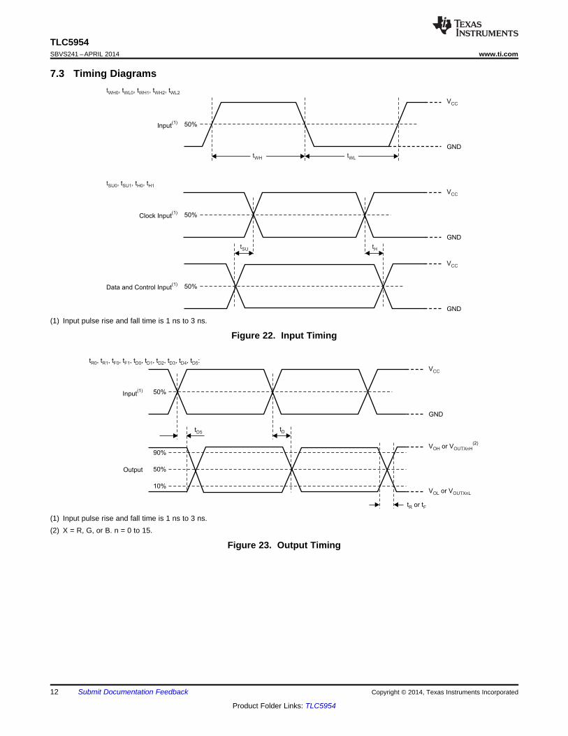
7.3 Timing Diagrams
(1) Input pulse rise and fall time is 1 ns to 3 ns.
Figure 22. Input Timing
(1) Input pulse rise and fall time is 1 ns to 3 ns.(2) X = R, G, or B. n = 0 to 15.
Figure 23. Output Timing
12 Submit Documentation Feedback Copyright © 2014, Texas Instruments Incorporated
Product Folder Links: TLC5954

t , tR0 F0
SIDB15B
Output current is changedby BC data changes.
ONB15B
tSU1
tWH1
L
1 2 3 4 5 6
HSIDG0B
SIDG0A
SIDR0A
Common Shift Register Bit 1(Internal)
LHONB0B
ONG0B
ONG14B
ONB14B
ONR15B
LSIDR0A
ONG0B
ONB0B
ONG14B
ONG15B
tWL0
New Data
tD0
VOUTXnL
SOUT
(Common shift register bit48)
ONR0B
ONG0B
SIDR0B
tH1
tF1
SIDB15B
HSIDR0B
tD3
tD3
tD3
tD4
tR1
SIDR0A
ONR0A
L
SCLK
OUTR0ON
OFF
LAT
On or Off Data Latch(Internal)
BLANK
ON
OFF
ON
OFF
ON
OFF
tWH0
tSU0 tH0 fCLK(SCLK)
47 48 49
MC1
SIDG15A
SIDR15A
SIDB14A
SIDG14A
SIDR14A
SIDG0A
SIDG15B
SIDR15B
SIDG0B
SIDB15A
1 2 3 4 47 48 49
Old Data (B15A to R0A = All 1s) New Data(OUTBn, OUTGn = All 1s , OUTRn = All 0s)
MC2
VOUTXnH
Global BC, FC Data Latch(Internal)
OUTG0
ON
OFF
ON
OFF
Common Shift Register Bit 0(Internal)
HONB15B
ONG15B
ONB15B
ONG15B
ONR15B
ONB0B
ONR1B
L
Common Shift Register Bit 47(Internal)
tWH2
tD2
SIDR0A
SIDG15A
SIDR15A
SIDB14A
SIDG14A
SIDR14A
SIDR15B
SIDB14B
SIDG14B
tD4
tD4
tD2
tD1
tWL2
ONB14B
SIDB13A
ONR14B
ONB14B
ONB15B
ONR15BSIN
ONR0B
Output on or off data write. FC, BC, MC data write.
SIDG0A
L
H H L L MC0
MC0
MC1
Old Data
MC1
MC2
L
MC2
BCR0
SIDR0B
H
SIDB15A
L
SIDG15B
HSIDB14B
H
SID are loaded into the commonshift register at the LAT signalrising time for on or off data writes.
SID are not loaded into the commonshift register at the LAT signal risingtime for BC, FC data writes.
SIDR0B
H
OUTB0
OUTR1
OUTG7
OUTB7
TLC5954www.ti.com SBVS241 –APRIL 2014
Timing Diagrams (continued)
(1) X = R, G, or B. n = 0 to 15.
Figure 24. Data Write and OUTXn On or Off Timing Diagram
Copyright © 2014, Texas Instruments Incorporated Submit Documentation Feedback 13
Product Folder Links: TLC5954

SIN
LAT
On or Off ControlData Latch
(Internal)Old On or Off Data
SCLK
47 48 491 2 3
Data are all 0(outputs are all off).
L
Power-Save Mode(PSM) Status
(Internal)Normal Mode
Power-Save Mode
Normal ModeNormal Mode
BLANK L
PSMODE Bit inFC Data
(Internal)01b
OFF
ON
OFF
OUTR0
OFF
ON
OFF
OUTG0
ON
OFF
OUTB7
ICC(VCC Current)
tD5
tSU2
H
H
(Outputs are not all off.)
ON
OFF
ON
OFF
ON
OFF
48 491 2
Normal Mode
The measured point is 90% ICC.
OFF
Data are not all 0 (outputs are not all off).
TLC5954SBVS241 –APRIL 2014 www.ti.com
Timing Diagrams (continued)
Figure 25. Power-Save Mode Timing Diagram (PSMODE = 01b)
14 Submit Documentation Feedback Copyright © 2014, Texas Instruments Incorporated
Product Folder Links: TLC5954

SIN
LAT
On or Off ControlData Latch
(Internal)
Old On or Off Data
SCLK
47 48 491 2 3
L
Power-Save Mode(PSM) Status
(Internal)Normal Mode Normal Mode
BLANK L
PSMODE Bit inFC Data
(Internal)
10b
OFF
ON
OFF
OUTR0
OFF
ON
OUTG0
OFF
ON
OUTB7
ICC(VCC Current)
tD5
(Outputs Are Not All Off) New Data Are All 0(Outputs Are All Off)
Power-SaveMode
Normal Mode
OFF
OFF
tSU3
H
H
Data Are Not All 0 (Outputs Are Not All Off)
Power-Save Mode
ON
OFF
OFF
ON
OFF
47 48 491 2
The measured point is 90% ICC.
ON
TLC5954www.ti.com SBVS241 –APRIL 2014
Timing Diagrams (continued)
Figure 26. Power-Save Mode Timing Diagram (PSMODE = 10b)
Copyright © 2014, Texas Instruments Incorporated Submit Documentation Feedback 15
Product Folder Links: TLC5954

TLC5954SBVS241 –APRIL 2014 www.ti.com
8 Detailed Description
8.1 OverviewThe TLC5954 is 48-channel, 34.9-mA or 24.4-mA, constant-current LED driver that can control the LED on of offsettings with the BLANK signal for grayscale (GS) control. The minimum 40-ns BLANK signal pulse duration canbe input to generate very short LED on-time.
The device has a 128-step, 7-bit, output current control function termed global brightness control (BC) that cancontrol each color group output. The BC function can adjust the red, green, and blue LED intensity for true whitewith constant-current control. The device contributes higher image quality to LED displays with fine white balancetuning by using these BLANK pulse durations and MC, BC functions.
The display controller can locate LED lamp failures via the device because the controller can detect LED lampfailures with the LED open detection (LOD) and LED short detection (LSD) functions. Furthermore, the reliabilityof the display can be improved by the LOD and LSD function.
The device maximum constant-current output value can be set by an internal register data function referred to asmaximum current control (MC), instead of the general method of using an external resistor setting. Thus, anyfailure modes that occur from the external resistor can be eliminated. One resistor can also be eliminated withthe MC function.
The device constant-current output can drive approximately 17.4 mA at a 0.32-V output voltage and a +25°Cambient temperature. This voltage is called knee voltage. This 0.32-V, low-knee voltage can contribute to thedesign of a lower-power display system.
The total number of LED drivers on one LED display panel can be reduced because 48 LED lamps can be drivenby one LED driver. Therefore, designing fine-pitch LED displays is simplified.
16 Submit Documentation Feedback Copyright © 2014, Texas Instruments Incorporated
Product Folder Links: TLC5954

MC
LODVLT, LSDVLT
3
8
77
Power-Save
Control
40-Bit MC, BC, FC Data Latch
48
40
MSB
VCC
SIN
BLANK
49-Bit Common Shift Register
48-Bit Output On or Off Data Latch
OUTR0
VCC
32-ChannelConstant-Current Sink Driver
LED Open Detection (LOD)LED Short Detection (LSD)
OUTR15
48
21
GND
LSB
LSB MSB
0 48
0 47
LSB MSB
0 39
SCLK
LAT
On or Off Control withOutput Delay
SOUT
OUTG0
OUTG15
48
7-Bit GlobalBC for OUTRn
16327 7 7
OUTB0
OUTB15
48-Bit LOD or LSDData
UVLO RESET
SIDHolder
To AllAnalog
Circuits
ALLOFF
RESET
48
2
2
78
48
2
2
10110010b
1Bits 47-40
bit 48
PSMODE
ALLOFF
33
SIDLD
BC
5
GND
GND
ThermalPad
ReferenceCurrentControl
DetectionVoltage
8-BitDecoder
7-Bit GlobalBC for OUTGn
7-Bit GlobalBC for OUTBn
16-Channel Constant-Current Sink Driver
TLC5954www.ti.com SBVS241 –APRIL 2014
8.2 Functional Block Diagram
Copyright © 2014, Texas Instruments Incorporated Submit Documentation Feedback 17
Product Folder Links: TLC5954

SCK
SINSOUT
Common Shift Register (49 bits)
LSBMSB
Bit 47 Bit 46 Bit 45 Bit 44 Bit 43 Bit 5 Bit4 Bit 3 Bit 2 Bit 1 Bit 0
SelectedSID forOUTR0
Selected SID (48 bits) by SIDLD data in the function control data latch.
SelectedSID forOUTG0
SelectedSID forOUTB0
SelectedSID forOUTR1
SelectedSID forOUTG1
SelectedSID forOUTB1
SelectedSID for
OUTG14
SelectedSID for
OUTB14
SelectedSID for
OUTR15
SelectedSID for
OUTG15
SelectedSID for
OUTB15
Selected SID by FC dataare loaded to the lower48 bits of the commonshift register when theLAT rising edge is inputwith 0 MSB data of thecommon shift register.
Bit 48
(0)
127
BCXI (mA) = I (mA)OLCMax ´OUTn
0.06 + 0.94 ´
TLC5954SBVS241 –APRIL 2014 www.ti.com
8.3 Feature Description
8.3.1 Output Current CalculationThe output current value controlled by MC and BC can be calculated by Equation 1.
where:• IOLCMax = the maximum constant-current value for all OUTXn for each color group programmed by MC data,• BCX = the global brightness control value (0h to 7Fh),• X = R, G, or B for the red, green, or blue color group, and• n = 0 to 15. (1)
Each output sinks the IOLCMax current when they turn on and the global brightness control (BC) data are set to themaximum value of 7Fh (127d).
8.3.2 Status Information Data (SID)The status information data (SID) contains the status of the LED open detection (LOD) and LED short detection(LSD).
When the output on-off data latch is written, the SID selected by the SIDLD bits are loaded into lower 48 bits inthe common shift register at the LAT rising edge after the original data in the common shift register are copied tothe on-off data latch. When the BC and FC data are written, SID data are not loaded to the common shiftregister. After SID data are copied into the common shift register, new SID data are not loaded until new data arewritten into the common shift register even if a LAT rising edge is input.
When the device resumes normal operation after the power-save mode, a BLANK rising edge must be input aftertSU2 or tSU3 elapses in order to retain correct LOD and LSD data in the SID holder because the SID analog circuitdoes not function during power-save mode. The SID load configuration and SID read timing are shown inFigure 27 and Figure 28, respectively.
Figure 27. SID Load Configuration
18 Submit Documentation Feedback Copyright © 2014, Texas Instruments Incorporated
Product Folder Links: TLC5954

SID47A
New On or Off Data (B15B-R0B)
SID1A
Detector Data0000h
SID47A
DetectorXXXXh
The detector data are not stable immediately after the BLANK signal goes low.
ONG0A
SID47B
SID0A
SID0A
SID0A
L
ONB15B
SID47A
SID0A
ONG15C
ONB15C
ONG15B
ONB15B
ONR0A
ONB0B
1 2 3 ---46 47 48 49
SIN
LAT
Output On or OffData Latch
(Internal)
SOUT
ONR15B
ONB6B
ONR0B
ONG0B
ONR1B
Old On or Off Data
SCLK
1 2 3 4 5
ONR15C
SID46B
BLANK
ONR0B
ONR0A
Shift RegisterLSB Data(Internal)
SID0B
SID0B
Shift RegisterLSB +1 Data
(Internal)
SID1B
SID46B
ONB15A
SID46A
SID45A
SID44A
SID43A
SID1A
SID45B
Shift RegisterMSB-1 Data
(Internal)
SID47B
SID47B
SID1A
SID46A
SID45A
SID44A
SID2A
SID46B
Shift RegisterMSB Data(Internal)
L
SIDLD in FCData Latch
(Internal)
ONG0B
ONB15B
L
47 48 49
ONG0A
ONB0A
SID Holder Data(Internal)
XXb
48-Bit LOD or LSDCircuit Output Data
(Internal)
Detector Data0000h
Detector DataXXXXh
Detector DataXXXXh
Detector DataXXXXh
Selected detector data by SIDLD are held in the SID holder when BLANK is high. The held data are loaded into the common shift registeras SID except when SIDLD is 00h.
LOD data go through the SID holder when BLANK is low.
48-Bit SID Data
LOD data are selected when SIDLD = 01h. LSD data are selected when SIDLD is set to 10b.No SID data are loaded when SIDLD is 00h or 11h.
New On or Off Data (B15A-R0A)
SID data selected by the SIDLD bit of FC data are loaded into thecommon shift register at the LAT rising edge except SIDLD = 00b.
ONG15B
ONR6B
ONB0B
ONG0B
ONR1B
ONB15C
ONG0A
ONB0A
ONR1A
ONG15B
ONB15B
ONB0B
ONR1B
ONG1B
SID0
SID1
SID0
LSID0A
SID1A
SID46A
SID45A
SID44A
SID2AL
SID0
SID1
L L
L
L L
LL
TLC5954www.ti.com SBVS241 –APRIL 2014
Feature Description (continued)
Figure 28. SID Read Timing Diagram
Copyright © 2014, Texas Instruments Incorporated Submit Documentation Feedback 19
Product Folder Links: TLC5954

LSD Data
OUTXn
VLOD
LOD Data
VLED
VLSD
LED Lamp
GND
1 = Error
1 = Error
On or OffControl
2.9 mA to 34.9 mA (for OUTRn, OUTGn)2.0 mA to 24.4 mA (for OUTBn)with Maximum BC Data
TLC5954SBVS241 –APRIL 2014 www.ti.com
Feature Description (continued)8.3.3 LED Open Detection (LOD)LOD detects a fault caused by an open circuit in the nth LED string, or a short from OUTXn to ground with lowimpedance, by comparing the OUTXn voltage to the LOD detection threshold voltage level set by LODVLT in thefunction control data latch (see Table 6 and Table 8). If the OUTXn voltage is lower than the programmedvoltage, the corresponding output LOD bit is set to 1 to indicate a shorted LED. Otherwise, the LOD bit is set to0. LOD data are only valid for outputs that are set to 1 in the output on-off data latch. LOD data are always 0 foroutputs that are set to 0 in the output on-off data latch.
LOD data are stored in a 48-bit register called the SID holder (see the Functional Block Diagram) at the BLANKrising edge when the SIDLD bits are set to 01b (see Table 7). The loaded LOD data can be read out through thecommon shift register as SID data at the SOUT pin. LOD data are not valid for 1 μs after the output is turned on.If the OUTXn controlled by the BLANK pin is less than 1 µs, the LOD data must be ignored.
When the device resumes operation from power-save mode, all OUTXn can be controlled by the internal on-offcontrol data and the BLANK level after the setup time (tSU2) elapses. LOD data are valid after the propagationdelay. Figure 29 illustrates an LOD and LSD circuit, Table 1 shows the SID bit settings for LOD and LSD, andFigure 30 illustrates the LED open-detection operating timing diagram.
Figure 29. LOD, LSD Circuit
Table 1. LOD, LSD Truth TableCORRESPONDING BITLOD LSD IN SID
LED is not open (VOUTXn > VLOD) LED is not shorted (VOUTXn ≤ VLSD) 0LED is shorted between anode and cathode, orLED is open or shorted to GND (VOUTXn ≤ VLOD) 1shorted to higher voltage side (VOUTXn > VLSD)
20 Submit Documentation Feedback Copyright © 2014, Texas Instruments Incorporated
Product Folder Links: TLC5954

BLANK L
Old output on or off data.
LAT
H
SID Holder Data(Internal)
LOD data go through the SID holderwhen BLANK is low.
SIDLD in FCData Latch
(Internal)01b
48-bit data are held in theSID holder when BLANK is high.
OUTXn Currentfor LED Lighting 0mA 0 mA
LOD = XXXXhOld data
2 mA to 34.9 mA (for OUTRn, OUTGn),1.4 mA to 24.4 mA (for OUTBn)when BC data are maximum.
48-bit LOD data are not stable for1 µs after BLANK goes low.
48-Bit LODCircuit Output Data
(Internal)
LOD = XXXXhLOD = 0000h LOD = 0000h
48-Bit CommonShift Register
(Internal)
LOD data (XXXXh) are loadedinto the shift register.
Latched in output on or off data.
New output on or off data.48-Bit Output
On or Off Data Latch(Internal)
TLC5954www.ti.com SBVS241 –APRIL 2014
Figure 30. LOD Operation Timing Diagram
8.3.4 LED Short Detection (LSD)LSD data detect a fault caused by a shorted LED by comparing the OUTXn voltage to the LSD detectionthreshold voltage level set by LSDVLT in the function control data latch (see Table 6 and Table 9). If the OUTXnvoltage is higher than the programmed voltage, the corresponding output LSD bit is set to 1 to indicate a shortedLED. Otherwise, the LSD bit is set to 0. LSD data are only valid for outputs that are set to 1 in the output on-offdata latch. LSD data are always 0 for outputs that are set to 0 in the output on-off data latch.
LSD data are loaded into a 48-bit register called the SID holder at the BLANK rising edge when the SIDLD bitsare set to 10b (see Table 7). The loaded LSD data can be read out through the common shift register as SIDdata at the SOUT pin. LSD data are not valid for 1 μs after the output is turned on. If the OUTXn controlled bythe BLANK pin is less than 1 µs, the LSD data must be ignored.
Copyright © 2014, Texas Instruments Incorporated Submit Documentation Feedback 21
Product Folder Links: TLC5954

BLANK L
Old output on or off data.
LAT
H
SID Holder Data(Internal)
LOD data go through the SID holderwhen BLANK is low.
SIDLD in FCData Latch
(Internal)10b
48-bit data are held in the SID holderwhen BLANK is high.
OUTXn Currentfor LED Lighting 0 mA 0 mA
LSD = XXXXhOld Data
48-bit LSD data are not stable for
1 s after BLANK goes low.m
48-Bit LSDCircuit Output Data
(Internal)LSD = XXXXhLSD = 0000h LSD = 0000h
48-Bit OutputOn or Off Data
(Internal)
2 mA to 34.9 mA (for OUTRn, OUTGn),1.4 mA to 24.4 mA (for OUTBn)when BC data are maximum.
LSD data (XXXXh) are loadedinto the shift register.
Latched output on or off data.
48-Bit CommonShift Register
(Internal)
New output on or off data.
TLC5954SBVS241 –APRIL 2014 www.ti.com
When the device resumes operation from power-save mode, all OUTXn can be controlled by the internal on-offcontrol data and the BLANK level after the setup time (tSU2) elapses. LSD data are valid after the propagationdelay. Figure 29 illustrates an LOD and LSD circuit and Figure 31 shows LED short-detection operating timingdiagram.
Figure 31. LSD Operation Timing Diagram
8.3.5 Noise ReductionLarge surge currents may flow through the device and the board on which the device is mounted if all 48 LEDchannels turned on simultaneously when BLANK toggles from high to low. These large current surges caninduce detrimental noise and electromagnetic interference (EMI) into other circuits. The device turns on the LEDchannels in a series delay to provide a circuit soft-start feature. A small delay circuit is implemented betweeneach output. When all bits of the on-off data latch are set to 1, each constant-current output turns on in thefollowing order: OUTR0, OUTG0, OUTB0, OUTR15, OUTG15, OUTB15, OUTR1, OUTG1, OUTB1, OUTR14,OUTG14, OUTB14, OUTR2, OUTG2, OUTB2, OUTR13, OUTG13, OUTB13, OUTR3, OUTG3, OUTB3,OUTR12, OUTG12, OUTB12, OUTR4, OUTG4, OUTB4, OUTR11, OUTG11, OUTB11, OUTR5, OUTG5,OUTB5, OUTR10, OUTG10, OUTB10, OUTR6, OUTG6, OUTB6, OUTR9, OUTG9, OUTB9, OUTR7, OUTG7,OUTB7, OUTR8, OUTG8, and OUTB8 with a small delay for each OUTXn after BLANK goes low or LAT goeshigh, see Figure 24. Both turn-on and turn-off times are delayed.
22 Submit Documentation Feedback Copyright © 2014, Texas Instruments Incorporated
Product Folder Links: TLC5954

TLC5954www.ti.com SBVS241 –APRIL 2014
8.4 Device Functional Modes
8.4.1 Maximum Constant Sink CurrentThe maximum output current of each channel (IOLCMax) is programmed by maximum current (MC) data and canbe set by the serial interface.
IOLCMax is the highest current for each output. Each OUTXn sinks IOLCMax current when they turn on with theglobal brightness control (BC) data set to the maximum value of 7Fh (127d). MC data are updated when thesame data are written to the MC bits twice. When the device is powered on, the MC data latch is set to 0.
Table 2 shows the characteristics of the constant-current sink versus the MC control data.
Table 2. Maximum Constant-Current Output versus MCData
MC DATA IOLCMax (mA)OUTRn,BINARY DECIMAL HEX OUTBnOUTGn
000 (default) 0 (default) 0 (default) 2.9 2.0001 1 1 4.4 3.1010 2 2 5.8 4.1011 3 3 8.7 6.1100 4 4 11.6 8.1101 5 5 17.4 12.2110 6 6 23.2 16.3111 7 7 34.9 24.4
8.4.2 Global Brightness Control (BC) Function: Sink Current ControlThe device is capable of simultaneously adjusting the output current of each color group (OUTR0 to OUTR15,OUTG0 to OUTG15, and OUTB0 to OUTB15). This function is called global brightness control (BC). The BCfunction allows the global BC data of LEDs connected to the three color groups to be adjusted. All OUTXn canbe adjusted in 128 steps from 6% to 100% of the maximum output current, IOLCMax. The BC data are transmittedto the device by the serial interface. When BC data change, the output current also changes immediately.
Table 3 shows the BC data versus the constant-current ratio against IOLCMax.
Table 3. BC Data versus Current Ratio and Set Current ValueBC DATA OUTPUT CURRENT (mA, typ)
OUTPUTBINARY OUTRn, OUTGn OUTBnCURRENTRATIO TO MC = 7h MC = 0h MC = 7h MC = 0h
IOLCMax (IOLCMax = 34.9 (IOLCMax = 2.9 (IOLCMax = 24.4 (IOLCMax = 2.0MSB LSB DECIMAL HEX (%, typ) mA) mA) mA) mA)
000 0000 0 00 6.0 2.09 0.17 1.47 0.12000 0001 1 01 6.7 2.35 0.20 1.65 0.14000 0010 2 02 7.5 2.61 0.22 1.83 0.15
… … … … … … … …111 1101 125 7D 98.5 34.4 2.86 24.1 1.96111 1110 126 7E 99.3 34.7 2.88 24.3 1.98111 1111 127 7F 100.0 34.9 2.90 24.4 2.00
Copyright © 2014, Texas Instruments Incorporated Submit Documentation Feedback 23
Product Folder Links: TLC5954

TLC5954SBVS241 –APRIL 2014 www.ti.com
8.4.3 Constant-Current Output On or Off ControlWhen BLANK is low, each OUTXn is controlled by the data in the output on or off data latch. When datacorresponding to an output equal 1, the output turns on; when data corresponding to an output equal 0, theoutput turns off. When BLANK is high, all OUTXn are forced off. When the device is powered on, the data in theoutput on or off data latch are set to 0. A truth table for the on or off control data is shown in Table 4.
Table 4. On or Off Control Data Truth TableON OR OFF CONTROL DATA CONSTANT-CURRENT OUTPUT STATUS
0 (default) Off1 On
8.4.4 Power-Save ModeThe power-save mode control bits are assigned in the BC and FC data latch. The device dissipation currentbecomes 7 μA (typ) in this mode. In PSM, all analog circuits (such as the constant-current outputs and the LODand LSD circuit) do not function. However, logic circuits (such as the common shift register, on-off data latch, andBC and FC data latch) do function. When the two bits in PSMODE are 01b, 10b, or 11b, the power-save mode isenabled. When the two bits are 11b, the device is always in power-save mode. When the two bits are set to 00b,the device is always in normal operation. If all 0s are written in the output on-off data latch, the device goes intopower-save mode when the two bits are 01b or 10b. When a rising edge is generated at SCLK with the twoPSMODE bits set to 01b, the device exits PSM and returns to normal operation. When data in the output on-offdata latch are not all 0s, and when the two PSMODE bits set to 10b, the device exits PSM and returns to normaloperation. All OUTXn are turned on after the device exits PSM. Figure 32 and Figure 33 provide power-savemode timing diagrams for PSMODE set to 01b and 10b, respectively. The BLANK level should go low after tSU2or tSU3 when the device exists PSM and returns to normal mode because the output current may be unstableimmediately after starting normal mode.
24 Submit Documentation Feedback Copyright © 2014, Texas Instruments Incorporated
Product Folder Links: TLC5954

When the device resumes normal mode, BLANK should be low afterthe setup time (for at least t ) from the SCLK rising edge input time
for stable output current.su2
7 µA (typ)
Power-SaveMode
SIN
LAT
SCLK
491 2
All Data Are 0
L
Power-SaveMode Status
Normal Mode Normal Mode
H
PSMODE Bit inFC Data Latch
(Internal)
01b
all OFFOUTXn
ICC(VCC Current)
more than 1mA
ON or OFF
BLANK L
491 2
Data Are Not 0
48-Bit CommonShift Register
(Internal)
SID holder data are loaded to the shift register at the LAT rising edge.
SID Holder Data(Internal)
SOUT
SID = XXXXh
48-Bit LODCircuit Output Data
(Internal)
LOD = XXXXh
LOD = XXXXh
48-bit LOD data are not stablefor 1 µs after BLANK goes low.
LOD = 0000h
48-Bit OutputOn or Off Data
(Internal)
491 2
SIDLD Bit inFC Data Latch
(Internal)01b
LOD = XXXXh
Data Are Not 0 Data Are Not 0
SID = 0000h
LOD = 0000h
ON or OFF ON or OFF
LOD = XXXXh
LOD = XXXXh
LOD = XXXXh
NormalMode
LOD = 0000h
L L
SID = XXXXh
LOD data are all0 because all outputs are off.
1
L
TLC5954www.ti.com SBVS241 –APRIL 2014
Figure 32. Power-Save Mode (FC Data PSMODE Bits = 01b)
Copyright © 2014, Texas Instruments Incorporated Submit Documentation Feedback 25
Product Folder Links: TLC5954

When the device resumes normal mode, BLANK should be lowafter the setup time for at least t from the SCLK rising edge
input time for stable output current.su3
7 µA (typ)
Power-Save Mode
SIN
LAT
SCLK
491 2
All Data = 0
L
Power-SaveMode Status
Normal Mode Normal Mode
H
PSMODE Bit inFC Data Latch
(Internal)10b
All OFFOUTXn
ICC (VCC Current)More than 1 mA
ON or OFF
BLANK L
491 2
Data Are Not 0
48-Bit CommonShift Register
(Internal)
SID holder data are loaded to the shift register at the LAT rising edge.
SID Holder Data(Internal)
SOUT
SID = XXXXh
48-Bit LODCircuit Output Data
(Internal)
LOD = XXXXh
LOD = XXXXh
48-bit LOD data are not stablefor 1 s after BLANK goes low.m
LOD = 0000h
48-Bit OutputOn or Off Data
(Internal)
491 2
SIDLD Bit inFC Data Latch
(Internal)01b
LOD = XXXXh
Data Are Not 0 Data Are Not 0
SID = 0000h
LOD = 0000h
ON or OFFONor OFF
LOD =XXXXh
LOD =XXXXh
LOD = XXXXh
LOD = 0000h
L L
SID = XXXXh
LOD data are all 0 because alloutputs are off.
1
L
TLC5954SBVS241 –APRIL 2014 www.ti.com
Figure 33. Power-Save Mode (FC Data PSMODE Bits = 10b)
26 Submit Documentation Feedback Copyright © 2014, Texas Instruments Incorporated
Product Folder Links: TLC5954
BC for
OUTB0-15
8-Bit WriteCommand Decoder,
96h (10010110b)
BC, FC Data Latch (37 Bits)
CommonData bit
43 SCK
SINSOUT
Common Shift Register (49 Bits)
LSB
CommonData bit
0
CommonData bit
1
CommonData bit
2
MSB
CommonData bit
46
CommonData bit
47
48 Bits
CommonData bit
45
CommonData bit
44
CommonData bit
5
CommonData bit
4
CommonData bit
3
This latch pulse isgenerated when LATrising edge is inputwith “0” MSB data ofcommon shift register(Data select bit).
Middle 37 Bits
LSB
0123454344454647 ---
0---29---16---23 17
Output On or Off Data Latch (48 Bits)
LSB
OUTR0On
MSB
OUTG0On
OUTB0On
OUTR1On
OUTG1On
OUTB1On
OUTG14On
OUTB14On
OUTR15On
OUTG15On
OUTB15On
0123454344454647 ---
48 Bits
Latch
MSB LSB
DataSelect bit
48
This latch pulse is generated when the LAT rising edge is inputwith the MSB data of the common shift register = 1 (data select bit).
FC for SIDLD, LODVLT,LSDVLT, PSMODE and
7-Bit Reserved Bit
---39 24
MSB
47 --- 40
Higher 8 Bits
48 Bits
BC forOUTR0-15
MC forAll
OUTXn
3---
BC forOUTG0-15
10
Theprevious
MC data
Lower 3 Bits
MC Data Latch (3 Bits)
Pre-MC Data Latch(3 Bits)
LSB MSB
Xlat
LatMC
3 Bits
XresetRESET from UVLO
3 Bits 3 Bits
3 Bits
3 Bits
TLC5954www.ti.com SBVS241 –APRIL 2014
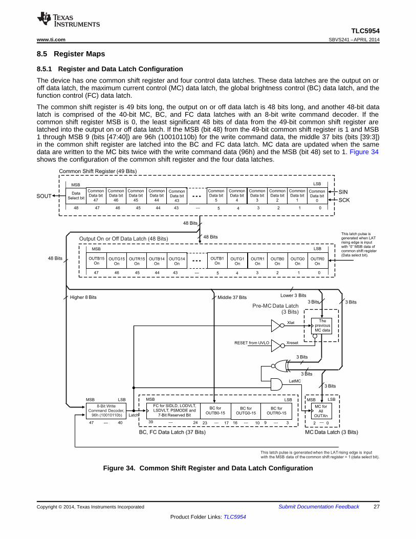
8.5 Register Maps
8.5.1 Register and Data Latch ConfigurationThe device has one common shift register and four control data latches. These data latches are the output on oroff data latch, the maximum current control (MC) data latch, the global brightness control (BC) data latch, and thefunction control (FC) data latch.
The common shift register is 49 bits long, the output on or off data latch is 48 bits long, and another 48-bit datalatch is comprised of the 40-bit MC, BC, and FC data latches with an 8-bit write command decoder. If thecommon shift register MSB is 0, the least significant 48 bits of data from the 49-bit common shift register arelatched into the output on or off data latch. If the MSB (bit 48) from the 49-bit common shift register is 1 and MSB1 through MSB 9 (bits [47:40]) are 96h (10010110b) for the write command data, the middle 37 bits (bits [39:3])in the common shift register are latched into the BC and FC data latch. MC data are updated when the samedata are written to the MC bits twice with the write command data (96h) and the MSB (bit 48) set to 1. Figure 34shows the configuration of the common shift register and the four data latches.
Figure 34. Common Shift Register and Data Latch Configuration
Copyright © 2014, Texas Instruments Incorporated Submit Documentation Feedback 27
Product Folder Links: TLC5954

TLC5954SBVS241 –APRIL 2014 www.ti.com
Register Maps (continued)8.5.1.1 Common Shift RegisterThe 49-bit common shift register is used to shift data from the SIN pin into the device. The data shifted into theregister are used for the output on or off control, MC, BC, and several FC functions, and the write command. TheLSB of the common shift register is connected to SIN and the MSB is connected to SOUT. On each SCLK risingedge, the data on SIN are shifted into the LSB and all 49 bits are shifted towards the MSB. The register MSB isalways connected to SOUT. In addition, the status information data (SID) selected by the SIDLD bits in the FCdata latch are loaded to the lower 48 bits of the 49-bit common shift register when a rising edge is input on LATfor the output on or off control data write operation except when SIDLD = 00b and 11b (see Table 7). When thedevice is powered on, all 49 bits of the common shift register are set to 0.
8.5.1.2 Output On or Off Data LatchThe output on or off data latch is 48 bits long and sets the on or off status for each constant-current output(OUTRn, OUTGn, OUTBn). When BLANK is low, the output corresponding to the specific bit in the output on oroff data latch is turned on if the data are 1 and remains off if the data are 0. When BLANK is high, all outputs areforced off, but the data in the latch do not change as long as LAT does not latch in new data. When the MSB ofthe common shift register is set to 0, the lower 48 bits are written to the output on or off data latch on the LATrising edge. When the device is powered on, all bits in the data latch are set to 0. The output on or off data latchbit assignment is shown in Table 5. See Figure 35 for an output on or off data write timing diagram.
Table 5. On or Off Control Data Latch Bit AssignmentCONTROL CONTROL
BIT LED BIT LEDNUMBER BIT NAME CHANNEL DESCRIPTION NUMBER BIT NAME CHANNEL DESCRIPTION
0 OUTR0ON OUTR0 24 OUTR8ON OUTR81 OUTG0ON OUTG0 25 OUTG8ON OUTG82 OUTB0ON OUTB0 26 OUTB8ON OUTB83 OUTR1ON OUTR1 27 OUTR9ON OUTR94 OUTG1ON OUTG1 28 OUTG9ON OUTG95 OUTB1ON OUTB1 29 OUTB9ON OUTB96 OUTR2ON OUTR2 30 OUTR10ON OUTR107 OUTG2ON OUTG2 31 OUTG10ON OUTG108 OUTB2ON OUTB2 32 OUTB10ON OUTB109 OUTR3ON OUTR3 33 OUTR11ON OUTR11
0 = Output off 0 = Output off10 OUTG3ON OUTG3 34 OUTG11ON OUTG111 = Output on with 1 = Output on with
11 OUTB3ON OUTB3 35 OUTB11ON OUTB11BLANK low. BLANK low.When the device is When the device is12 OUTR4ON OUTR4 36 OUTR12ON OUTR12powered on, all bits are powered on, all bits are
13 OUTG4ON OUTG4 37 OUTG12ON OUTG12set to 0. set to 0.14 OUTB4ON OUTB4 38 OUTB12ON OUTB1215 OUTR5ON OUTR5 39 OUTR13ON OUTR1316 OUTG5ON OUTG5 40 OUTG13ON OUTG1317 OUTB5ON OUTB5 41 OUTB13ON OUTB1318 OUTR6ON OUTR6 42 OUTR14ON OUTR1419 OUTG6ON OUTG6 43 OUTG14ON OUTG1420 OUTB6ON OUTB6 44 OUTB14ON OUTB1421 OUTR7ON OUTR7 45 OUTR15ON OUTR1522 OUTG7ON OUTG7 46 OUTG15ON OUTG1523 OUTB7ON OUTB7 47 OUTB15ON OUTB15
28 Submit Documentation Feedback Copyright © 2014, Texas Instruments Incorporated
Product Folder Links: TLC5954

TLC5954www.ti.com SBVS241 –APRIL 2014
Table 6. MC, BC, and FC Data Latch and Write Command Bit DescriptionDEFAULT
BIT BIT VALUENUMBER NAME (BINARY) DESCRIPTION
Maximum current control (MC) data for all OUTXn[2:0] MAXCUR (MC) 000b (data = 0h to 7h, see Table 2)Global brightness control (BC) data for RED color group[9:3] BCR (BC) — (data = 00h to 7Fh, see Table 3)Global brightness control (BC) data for GREEN color group[16:10] BCG (BC) — (data = 00h to 7Fh, see Table 3)Global brightness control (BC) data for BLUE color group[23:17] BCB (BC) — (data = 00h to 7Fh, see Table 3)SID load control. These two bits select the SID loaded to the common register
[25:24] SIDLD (FC) — when the LAT rising edge is input for on or off data writes. Table 7 shows theselected data truth table.LOD detection voltage select. These three bits select the detection threshold
[28:26] LODVLT (FC) — voltage for the LED open detection (LOD). Table 8 shows the detect voltagetruth table.LSD detection voltage select. These two bits select the detection threshold
[30:29] LSDVLT (FC) — voltage for the LED short detection (LSD). Table 9 shows the detect voltagetruth table.Power-save mode select. These two bits select the power-save mode between
[32:31] PSMODE (FC) 11b the four modes. Table 10 shows the power-save mode truth table. Figure 32and Figure 33 illustrate the power-save mode operation timing diagrams.
[39:33] RSV — Reserved data, don’t care.Write command. When this data are 96h (10010110b), MC, BC, and FC data
[47:40] WRTCMD — can be updated. In order to update MC data, the same data must be writtentwice to the MC bit.
Table 7. SID Load Control Truth TableSIDLD STATUS INFORMATION DATA (SID) LOADED TO THE COMMON SHIFT
BIT 25 BIT 24 REGISTER0 0 No data are loaded (default value)0 1 LED open detection (LOD) data are loaded1 0 LED short detection (LSD) data are loaded1 1 No data are loaded
Table 8. LOD Threshold Voltage Truth TableLODVLT
BIT 28 BIT 27 BIT 26 LED OPEN DETECTION (LOD) THRESHOLD VOLTAGE0 0 0 VLOD0 (0.20 V, typ)0 0 1 VLOD1 (0.30 V, typ)0 1 0 VLOD2 (0.40 V, typ)0 1 1 VLOD3 (0.50 V, typ)1 0 0 VLOD4 (0.60 V, typ)1 0 1 VLOD1 (0.30 V, typ)1 1 0 VLOD1 (0.30 V, typ)1 1 1 VLOD1 (0.30 V ,typ)
Copyright © 2014, Texas Instruments Incorporated Submit Documentation Feedback 29
Product Folder Links: TLC5954

TLC5954SBVS241 –APRIL 2014 www.ti.com
Table 9. LSD Threshold Voltage Truth TableLSDVLT
BIT 30 BIT 29 LED SHORT DETECTION (LSD) THRESHOLD VOLTAGE0 0 VLSD0 (0.50 × VCC, typ)0 1 VLSD1 (0.70 × VCC, typ)1 0 VLSD2 (0.90 × VCC, typ)1 1 VLSD2 (0.90 × VCC, typ)
Table 10. Power-Save Mode Truth TablePSMODE
BIT 32 BIT 31 POWER-SAVE MODE FUNCTION0 0 Power-save mode is disabled in every condition.
When all zeroes (0s) are written to the output on or off data latch, the device goesto power-save mode. When an SCLK rising edge occurs, the device goes tonormal operation and starts to control the output current. However, after the setuptime (tSU2) elapses from the SCLK input timing, BLANK must go low. Otherwise,0 1 the output current may not reach the set constant-current value. If these two bitsare set to 01b from 10b or 11b when the device is in power-save mode (PSM), thedevice remains in PSM and does not resume normal mode. When an SCLK risingedge is input after PSMODE = 01 is selected, the device returns to normal mode.When all zeroes (0s) are written to the output on or off data latch, the device goesto power-save mode. When the data (except all 0s) are written to the output on oroff data latch, the device goes to normal operation and starts to control the outputcurrent. However, after the setup time (tSU3) elapses from the LAT input timing,
1 0 BLANK must go low. Otherwise, the output current may not reach the set constant-current value. If this bit set is selected from other bit set to this bit set when thedevice is in PSM, the device remains in power-save mode. When data that are notall set to off are written to the on or off data latch after this bit set is selected, thedevice goes to normal mode.
1 (default) 1 (default) Power-save mode is enabled in every condition.
30 Submit Documentation Feedback Copyright © 2014, Texas Instruments Incorporated
Product Folder Links: TLC5954

ONB15A
ONR0A
ONR15B
OFF
SID47A
L
SID46A
SID45A
SID44A
SID47B
SID47B
ONG15C
ONB15C
SID0A
SID0A
SID0A
L
ONG15B
L
L
SID0A
ONB15C
LON
G15BON
B15BON
G14CONR0A
ONB0B
1 2 3 4 5 646 47 48 49
SIN
LAT
Output On or OffData Latch
(Internal)
SOUT
ONB14B
ONR0B
ONG0B
ONR1B
SCLK
1 2 3 4 5
ONG15C
ONR15C
ONB14C
SID46B
SID45B
SID44B
SID43B
BLANK
ONR0B
Common ShiftRegister LSB
(Internal)
SID0B
SID0B
ONG0A
ONR1B
ONB15B
ONB0B
ONG1B
ONR15C
ONB14C
Common ShiftRegister LSB +1
(Internal)
SID1B
SID46B
SID46A
SID1A
SID45B
SID44B
SID43B
SID42B
Common ShiftRegister MSB -1
(Internal)
SID47B
SID1A
SID2A
SID46B
SID45B
SID44B
SID43B
Common ShiftRegister MSB
(Internal)
BC data are not changed.
SID1A
SID47A
ONG0B
ONB15B
L
OFF
ON
OUTXn(1)
ON
OFFOFF
ON
ON
OFFOFF
ON
ON
OFF
ON
OFF
ON
OFFOFF
OFF
ON
On or Off Data
SID0A
SID47A
SID1A
SID46A
SID45A
SID44A
SID2A
ONB15B
LON
G15BON
R15BONB0B
ONG0B
ONR1B
ONG15C
ONB15C
ONR15C
ONB14C
ONG14C
SID45A
SID44A
SID43A
L
BC Data Latch(Internal)
L
OUTXn(2)
OUTXn(3)
OUTXn(4)
(B15A-R0A) On or Off Data (B15B-R0B)
TLC5954www.ti.com SBVS241 –APRIL 2014
(1) On or off latched data are 1.(2) On or off latched data change from 1 to 0 at the second LAT signal.(3) On or off latched data change from 0 to 1 at the second LAT signal.(4) On or off latched data are 0.
Figure 35. Output On or Off Timing Diagram: Data Write and OUTXn Control
Copyright © 2014, Texas Instruments Incorporated Submit Documentation Feedback 31
Product Folder Links: TLC5954
MC, BC, FC are selected whenthe MSB is high.
H
H
H
MC1A
MC0A
MC0A
MC0A
1 2 3 4 5 646 47 48 49
SIN
LAT
Output On or OffData latch(Internal)
SOUT
Old MC Data
SCLK
1 2 3 4 5
Common ShiftRegister LSB
(Internal)
MC0B
BCR0B
MC2B
BCR1B
Common ShiftRegister LSB +1
(Internal)
MC1B
MC0A
MC1A
Common ShiftRegister MSB-1
(Internal)H
MC1A
MC2A
Common ShiftRegister MSB
(Internal)H
MC Data Latch(Internal)
New MC data
H
LHMC0A
MC2B
L MC0B
MC1B
BCR0B
HH L
H LMC2B
MC0B
MC1B
BCR0B
H H L
H
H L
On or off control data are not changed.
MC0A
MC1A
MC2A
HL
L
H H L
H H L
LH
L
LH
H
MC, BC, FC data writes are selected when MSB -1 to MSB-9 bits are 96h (HLLHLHHL).
L
L H
L H
L
L LH
L
L
L
L
H LH
L
H
H L
H L H
LHH
Old FC DataFC Data Latch(Internal)
New FC data
Old BC DataBC Data Latch(Internal)
New BC data
MC data in the data latch are updated to new data only when thesame data are written twice with write command.(MC0B to MC2B data must be the same as MC0A to MC2A).
BC and FC data in the data latch are updated to new data when theMSB of the common shift resistor is 1 and write command bit(MSB-1 ~ MSB9) is 96h (10010110b).
TLC5954SBVS241 –APRIL 2014 www.ti.com
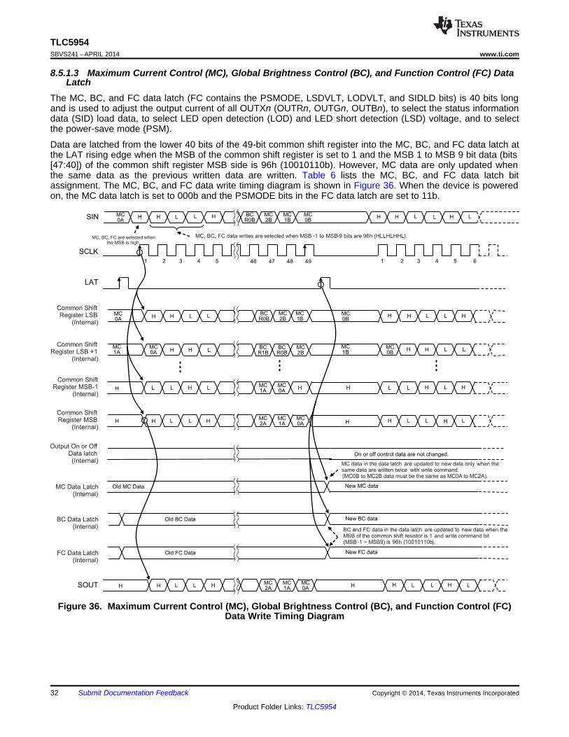
8.5.1.3 Maximum Current Control (MC), Global Brightness Control (BC), and Function Control (FC) DataLatch
The MC, BC, and FC data latch (FC contains the PSMODE, LSDVLT, LODVLT, and SIDLD bits) is 40 bits longand is used to adjust the output current of all OUTXn (OUTRn, OUTGn, OUTBn), to select the status informationdata (SID) load data, to select LED open detection (LOD) and LED short detection (LSD) voltage, and to selectthe power-save mode (PSM).
Data are latched from the lower 40 bits of the 49-bit common shift register into the MC, BC, and FC data latch atthe LAT rising edge when the MSB of the common shift register is set to 1 and the MSB 1 to MSB 9 bit data (bits[47:40]) of the common shift register MSB side is 96h (10010110b). However, MC data are only updated whenthe same data as the previous written data are written. Table 6 lists the MC, BC, and FC data latch bitassignment. The MC, BC, and FC data write timing diagram is shown in Figure 36. When the device is poweredon, the MC data latch is set to 000b and the PSMODE bits in the FC data latch are set to 11b.
Figure 36. Maximum Current Control (MC), Global Brightness Control (BC), and Function Control (FC)Data Write Timing Diagram
32 Submit Documentation Feedback Copyright © 2014, Texas Instruments Incorporated
Product Folder Links: TLC5954
¼
SIN
SCLK
LAT
BLANK
SOUT
GND
VCC
Device 1VCC
¼
¼
¼
SIN
SCLK
LAT
BLANK
SOUT
Device n
OUTR0 OUTB15
DATA
SCLK
BLANK
¼
Controller GND
VCC
VCC
3
LAT
¼
¼OUTR0 OUTB15
¼
SID Read
VLED
PowerPAD PowerPAD
GND GND
TLC5954www.ti.com SBVS241 –APRIL 2014
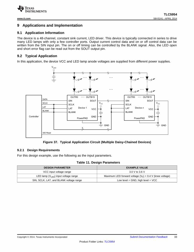
9 Applications and Implementation
9.1 Application InformationThe device is a 48-channel, constant sink current, LED driver. This device is typically connected in series to drivemany LED lamps with only a few controller ports. Output current control data and on or off control data can bewritten from the SIN input pin. The on or off timing can be controlled by the BLANK signal. Also, the LED openand short error flag can be read out from the SOUT output pin.
9.2 Typical ApplicationIn this application, the device VCC and LED lamp anode voltages are supplied from different power supplies.
Figure 37. Typical Application Circuit (Multiple Daisy-Chained Devices)
9.2.1 Design RequirementsFor this design example, use the following as the input parameters.
Table 11. Design ParametersDESIGN PARAMETER EXAMPLE VALUEVCC input voltage range 3.0 V to 3.6 V
LED lamp (VLED) input voltage range Maximum LED forward voltage (VF) + 0.4 V (knee voltage)SIN, SCLK, LAT, and BLANK voltage range Low level = GND, high level = VCC
Copyright © 2014, Texas Instruments Incorporated Submit Documentation Feedback 33
Product Folder Links: TLC5954

TLC5954SBVS241 –APRIL 2014 www.ti.com
9.2.2 Detailed Design Procedure
9.2.2.1 Step-by-Step Design ProcedureTo begin the design process, a few parameters must be decided upon. The designer needs to know thefollowing:• Maximum output constant-current value for all colors of the LED ramp.• Maximum LED forward voltage (VF).• Current ratio of red, green, and blue LED lamps for the best white balance.• Is the LED open detect (LOD) function used? If so, which detection level (0.20 V, 0.30 V, 0.40 V, 0.50 V, or
0.60 V) is used?• Is the LED short detect (LSD) function used? If so, which detection level (50% VCC, 70% VCC, or 90% VCC)
is used?
9.2.2.2 Maximum Current (MC) DataThere are a total of three bits of MC data that set the output current of all constant-current outputs (OUTXn).Select the MC data to be greater than the target LED ramp current if the output current is reduced whitebalanced by the global brightness control data and write the data with other control data.
9.2.2.3 Global Brightness Control (BC) DataThere are a total of three sets of 7-bit BC data for the red, green, and blue LED ramp. Select the BC data for thebest white balance of the red, green, and blue LED ramp and write the data with other control data.
9.2.2.4 On or Off DataThere are a total of 48 bits of on or off data for the on or off control of each output. Select the on or off data ofthe LED lamp on or off status control and write the data.
9.2.2.5 Other Control DataThere are a total of 8 bits of control data to set the function mode for the status information data (SID) loadcontrol, LOD voltage setting, LSD voltage setting, and power save mode (PSM) explained in the DeviceFunctional Modes section. Write the 8-bit control data for the appropriate operation of the display system with MCand BC data as the control data.
9.2.2.6 Grayscale ControlAll constant-current outputs are controlled by the BLANK pin logic level. When BLANK is GND, all constant-current outputs are turned on except that the output is set to 0 in the 48-bit output on-off data latch. WhenBLANK is VCC, all outputs are forced off. The LED lamp grayscale can be controlled by the BLANK low pulseduration.
34 Submit Documentation Feedback Copyright © 2014, Texas Instruments Incorporated
Product Folder Links: TLC5954

Ch4: BLANK (2V/div)
Ch1: VCC (2V/div)
Ch2: VLED (2V/div)
Ch3: Output current of VOUTB0 (10mA/div, BLUE LED
Ch4: BLANK (2V/div)
Ch1: VCC (2V/div)
Ch2: VLED (2V/div)
Ch3: Output current of VOUTR0 (10mA/div, RED LED
Ch4: BLANK (2V/div)
Ch1: VCC (2V/div)
Ch2: VLED (2V/div)
Ch3: Output current of VOUTG0 (10mA/div, GREEN LED
TLC5954www.ti.com SBVS241 –APRIL 2014
9.2.3 Application CurvesOne LED connected to each output. BLANK low pulse duration = 40 ns.
MCX = 5 BCX = 7Fh VLED = 4.2 V MCX = 5 BCX = 7Fh VLED = 4.2 VVCC = 3.3 V SIDLD = LODVLT = LSDVLT = PSMODE = 0 VCC = 3.3 V SIDLD = LODVLT = LSDVLT = PSMODE = 0
Figure 38. OUTR0 Output Current Waveform Figure 39. OUTG0 Output Current Waveform
MCX = 5 BCX = 7Fh VLED = 4.2 VVCC = 3.3 V SIDLD = LODVLT = LSDVLT = PSMODE = 0
Figure 40. OUTB0 Output Current Waveform
Copyright © 2014, Texas Instruments Incorporated Submit Documentation Feedback 35
Product Folder Links: TLC5954

TLC5954SBVS241 –APRIL 2014 www.ti.com
10 Power Supply Recommendations
The VCC power-supply voltage should be well regulated. An electrolytic capacitor must be used to reduce thevoltage ripple to less than 5% of the input voltage. Furthermore, the VLED voltage should be set to the voltagecalculated by Equation 2:VLED ≥ LED Maximum VF × Number of LED Lamps Connected in Series + 0.4 V (5 mA for MC Data Example)
where:• VF = Forward voltage (2)
Because the total current of the constant-current output is large, some electrolytic capacitors must be used toprevent the OUTXn pin voltage from dropping lower than the calculated voltage from Equation 2.
11 Layout
11.1 Layout Guidelines1. The decoupling capacitor should be placed near the VCC and GND pin.2. The GND pattern should be routed as widely as possible for large GND currents. Maximum GND current is
approximately 1.52 A.3. The routing between the LED cathode side and the device OUTXn should be routed to be as short and
straight as possible to reduce wire inductance.4. The PowerPAD should be connected to the GND layer because the pad is connected to GND internally. The
PowerPAD also should be connected to the heat sink layer to reduce device temperature.
36 Submit Documentation Feedback Copyright © 2014, Texas Instruments Incorporated
Product Folder Links: TLC5954

OU
TG
2
OU
TB
2
OU
TR
3
OU
TG
3
OU
TB
3
OU
TR
4
OU
TG
4
OU
TB
4
OU
TR
5
OU
TG
5
OU
TB
5
SIN
LA
T
SC
LK
VC
C
OU
TR
10
OU
TG
10
OU
TB
10
OU
TR
11
OU
TG
11
OU
TB
11
OU
TR
12
OU
TG
12
OU
TB
12
OU
TR
13
OU
TG
13
OU
TB
13
GN
D
BLANK
OUTR6
OUTG6
OUTB6
OUTR7
OUTG7
OUTB7
OUTR8
OUTG8
OUTB8
OUTR9
OUTG9
OUTB9
SOUT
VIA
Bottom-Side PCB Pattern
Top-Side PCB Pattern
GND
OUTR14
OUTG14
OUTB14
OUTR15
OUTG15
OUTB15
OUTR0
OUTG0
OUTB0
OUTR1
OUTG1
OUTB1
OUTR2
POWER
ToNextLAT
ToNext
BLANK
ToNext
SCLK
ToNextSINTo Next VCCTo Next GNDTo Next VLED
VLED GND VCC SIN
SCLK
BLANK
LAT
PowerPAD
TLC5954www.ti.com SBVS241 –APRIL 2014
11.2 Layout Example
Figure 41. Layout Example
Copyright © 2014, Texas Instruments Incorporated Submit Documentation Feedback 37
Product Folder Links: TLC5954

TLC5954SBVS241 –APRIL 2014 www.ti.com
12 Device and Documentation Support
12.1 Device Support
12.1.1 Development SupportFor the LED driver solution, go to www.ti.com/solution/lighting_signage.
12.2 Documentation Support
12.2.1 Related DocumentationFor related documentation see the following:• PowerPAD™ Thermally Enhanced Package Application Report, SLMA002
12.3 TrademarksAll trademarks are the property of their respective owners.
12.4 Electrostatic Discharge CautionThese devices have limited built-in ESD protection. The leads should be shorted together or the device placed in conductive foamduring storage or handling to prevent electrostatic damage to the MOS gates.
12.5 GlossarySLYZ022 — TI Glossary.
This glossary lists and explains terms, acronyms and definitions.
13 Mechanical, Packaging, and Orderable InformationThe following pages include mechanical packaging and orderable information. This information is the mostcurrent data available for the designated devices. This data is subject to change without notice and revision ofthis document. For browser-based versions of this data sheet, refer to the left-hand navigation.
38 Submit Documentation Feedback Copyright © 2014, Texas Instruments Incorporated
Product Folder Links: TLC5954

PACKAGE OPTION ADDENDUM
www.ti.com 10-Dec-2020
Addendum-Page 1
PACKAGING INFORMATION
Orderable Device Status(1)
Package Type PackageDrawing
Pins PackageQty
Eco Plan(2)
Lead finish/Ball material
(6)
MSL Peak Temp(3)
Op Temp (°C) Device Marking(4/5)
Samples
TLC5954RTQR ACTIVE QFN RTQ 56 2000 RoHS & Green NIPDAU Level-3-260C-168 HR -40 to 85 TLC5954
TLC5954RTQT ACTIVE QFN RTQ 56 250 RoHS & Green NIPDAU Level-3-260C-168 HR -40 to 85 TLC5954
(1) The marketing status values are defined as follows:ACTIVE: Product device recommended for new designs.LIFEBUY: TI has announced that the device will be discontinued, and a lifetime-buy period is in effect.NRND: Not recommended for new designs. Device is in production to support existing customers, but TI does not recommend using this part in a new design.PREVIEW: Device has been announced but is not in production. Samples may or may not be available.OBSOLETE: TI has discontinued the production of the device.
(2) RoHS: TI defines "RoHS" to mean semiconductor products that are compliant with the current EU RoHS requirements for all 10 RoHS substances, including the requirement that RoHS substancedo not exceed 0.1% by weight in homogeneous materials. Where designed to be soldered at high temperatures, "RoHS" products are suitable for use in specified lead-free processes. TI mayreference these types of products as "Pb-Free".RoHS Exempt: TI defines "RoHS Exempt" to mean products that contain lead but are compliant with EU RoHS pursuant to a specific EU RoHS exemption.Green: TI defines "Green" to mean the content of Chlorine (Cl) and Bromine (Br) based flame retardants meet JS709B low halogen requirements of <=1000ppm threshold. Antimony trioxide basedflame retardants must also meet the <=1000ppm threshold requirement.
(3) MSL, Peak Temp. - The Moisture Sensitivity Level rating according to the JEDEC industry standard classifications, and peak solder temperature.
(4) There may be additional marking, which relates to the logo, the lot trace code information, or the environmental category on the device.
(5) Multiple Device Markings will be inside parentheses. Only one Device Marking contained in parentheses and separated by a "~" will appear on a device. If a line is indented then it is a continuationof the previous line and the two combined represent the entire Device Marking for that device.
(6) Lead finish/Ball material - Orderable Devices may have multiple material finish options. Finish options are separated by a vertical ruled line. Lead finish/Ball material values may wrap to twolines if the finish value exceeds the maximum column width.
Important Information and Disclaimer:The information provided on this page represents TI's knowledge and belief as of the date that it is provided. TI bases its knowledge and belief on informationprovided by third parties, and makes no representation or warranty as to the accuracy of such information. Efforts are underway to better integrate information from third parties. TI has taken andcontinues to take reasonable steps to provide representative and accurate information but may not have conducted destructive testing or chemical analysis on incoming materials and chemicals.TI and TI suppliers consider certain information to be proprietary, and thus CAS numbers and other limited information may not be available for release.
In no event shall TI's liability arising out of such information exceed the total purchase price of the TI part(s) at issue in this document sold by TI to Customer on an annual basis.

PACKAGE OPTION ADDENDUM
www.ti.com 10-Dec-2020
Addendum-Page 2

TAPE AND REEL INFORMATION
*All dimensions are nominal
Device PackageType
PackageDrawing
Pins SPQ ReelDiameter
(mm)
ReelWidth
W1 (mm)
A0(mm)
B0(mm)
K0(mm)
P1(mm)
W(mm)
Pin1Quadrant
TLC5954RTQR QFN RTQ 56 2000 330.0 16.4 8.3 8.3 1.1 12.0 16.0 Q2
TLC5954RTQT QFN RTQ 56 250 180.0 16.4 8.3 8.3 1.1 12.0 16.0 Q2
PACKAGE MATERIALS INFORMATION
www.ti.com 23-Jun-2015
Pack Materials-Page 1

*All dimensions are nominal
Device Package Type Package Drawing Pins SPQ Length (mm) Width (mm) Height (mm)
TLC5954RTQR QFN RTQ 56 2000 367.0 367.0 38.0
TLC5954RTQT QFN RTQ 56 250 210.0 185.0 35.0
PACKAGE MATERIALS INFORMATION
www.ti.com 23-Jun-2015
Pack Materials-Page 2

www.ti.com
GENERIC PACKAGE VIEW
Images above are just a representation of the package family, actual package may vary.Refer to the product data sheet for package details.
VQFN - 1 mm max heightRTQ 56PLASTIC QUAD FLATPACK - NO LEAD8 x 8, 0.5 mm pitch
4224653/A

NOTES:
1. All linear dimensions are in millimeters. Any dimensions in parenthesis are for reference only. Dimensioning and tolerancingper ASME Y14.5M.
2. This drawing is subject to change without notice.3. The package thermal pad must be soldered to the printed circuit board for thermal and mechanical performance.
PACKAGE OUTLINE
www.ti.com
4225369 / A 10/2019
VQFN - 1 mm max height
PLASTIC QUAD FLATPACK-NO LEAD
RTQ0056G
A
0.08 C
0.1 C A B0.05 C
B
SYMM
SYMM
8.157.85
8.157.85
1 MAX
0.050.00
SEATING PLANE
PIN 1 INDEX AREA
C
5.6±0.1
5.6±0.14X6.5
PIN 1 ID(OPTIONAL)
1
14
15 28
29
42
4356
52X 0.5
56X 0.50.3
56X 0.300.18
(0.2) TYP
57

NOTES: (continued)
4. This package is designed to be soldered to a thermal pad on the board. For more information, see Texas Instrumentsliterature number SLUA271 (www.ti.com/lit/slua271).
5. Vias are optional depending on application, refer to device data sheet. If any vias are implemented, refer to theirlocations shown on this view. it is recommended thar vias under paste be filled, plugged or tented.
EXAMPLE BOARD LAYOUT
4225369 / A 10/2019
www.ti.com
VQFN - 1 mm max height
RTQ0056G
PLASTIC QUAD FLATPACK-NO LEAD
SYMM
SYMM
LAND PATTERN EXAMPLESCALE: 10X
(7.8)
1
14
15 28
29
42
4356
(0.78)
56X (0.24)
56X (0.6)
52X (0.5)
(R0.05)TYP
0.07 MAXALL AROUND 0.07 MIN
ALL AROUND
METAL
SOLDER MASKOPENING
SOLDER MASKOPENING
METAL UNDERSOLDER MASK
SOLDER MASK DETAILS
NON SOLDER MASKDEFINED
(PREFERRED)SOLDER MASK
DEFINED
57
(5.6)
(5.6)
(Ø0.2) TYPVIA
8X (1.33) 6X (1.22)
8X (1.33)
6X (1.22)

NOTES: (continued)
6. Laser cutting apertures with trapezoidal walls and rounded corners may offer better paste release. IPC-7525 may have alternatedesign recommendations..
EXAMPLE STENCIL DESIGN
4225369 / A 10/2019
www.ti.com
VQFN - 1 mm max height
RTQ0056G
PLASTIC QUAD FLATPACK-NO LEAD
SYMM
SYMM
SOLDER PASTE EXAMPLEBASED ON 0.125 mm THICK STENCIL
EXPOSED PAD66% PRINTED COVERAGE BY AREA
SCALE: 10X
1
14
15 28
29
42
4356
(7.8)
(7.8)
METALTYP
57
56X (0.24)
56X (0.6)
(R0.05) TYP
8X (0.665)
16X( 1.13)
52X (0.5)
8X (1.33)
8X (0.665)
8X (1.33)

IMPORTANT NOTICE AND DISCLAIMER
TI PROVIDES TECHNICAL AND RELIABILITY DATA (INCLUDING DATASHEETS), DESIGN RESOURCES (INCLUDING REFERENCE DESIGNS), APPLICATION OR OTHER DESIGN ADVICE, WEB TOOLS, SAFETY INFORMATION, AND OTHER RESOURCES “AS IS” AND WITH ALL FAULTS, AND DISCLAIMS ALL WARRANTIES, EXPRESS AND IMPLIED, INCLUDING WITHOUT LIMITATION ANY IMPLIED WARRANTIES OF MERCHANTABILITY, FITNESS FOR A PARTICULAR PURPOSE OR NON-INFRINGEMENT OF THIRD PARTY INTELLECTUAL PROPERTY RIGHTS.These resources are intended for skilled developers designing with TI products. You are solely responsible for (1) selecting the appropriate TI products for your application, (2) designing, validating and testing your application, and (3) ensuring your application meets applicable standards, and any other safety, security, or other requirements. These resources are subject to change without notice. TI grants you permission to use these resources only for development of an application that uses the TI products described in the resource. Other reproduction and display of these resources is prohibited. No license is granted to any other TI intellectual property right or to any third party intellectual property right. TI disclaims responsibility for, and you will fully indemnify TI and its representatives against, any claims, damages, costs, losses, and liabilities arising out of your use of these resources.TI’s products are provided subject to TI’s Terms of Sale (www.ti.com/legal/termsofsale.html) or other applicable terms available either on ti.com or provided in conjunction with such TI products. TI’s provision of these resources does not expand or otherwise alter TI’s applicable warranties or warranty disclaimers for TI products.
Mailing Address: Texas Instruments, Post Office Box 655303, Dallas, Texas 75265Copyright © 2020, Texas Instruments Incorporated