tmp121 tmp123 1.5 c accurate digital temperature sensor
TRANSCRIPT

FEATURES� DIGITAL OUTPUT: SPI-Compatible Interface
� RESOLUTION: 12-Bit + Sign, 0.0625 °C� ACCURACY:
±1.5°C from −25 °C to +85°C (max)
� LOW QUIESCENT CURRENT: 50µA (max)
� WIDE SUPPLY RANGE: 2.7V to 5.5V
� TINY SOT23-6 PACKAGE
� OPERATION TO 150°C
APPLICATIONS� POWER-SUPPLY TEMPERATURE
MONITORING
� COMPUTER PERIPHERAL THERMALPROTECTION
� NOTEBOOK COMPUTERS
� CELL PHONES
� BATTERY MANAGEMENT
� OFFICE MACHINES
DESCRIPTIONThe TMP121 and TMP123 are SPI-compatible tempera-ture sensors available in the tiny SOT23-6 package.Requiring no external components, the TMP121 andTMP123 are capable of measuring temperatures within2°C of accuracy over a temperature range of −40°C to+125°C. Low supply current, and a supply range from 2.7Vto 5.5V, make the TMP121 and TMP123 excellentcandidates for low-power applications.
The TMP121 and TMP123 are ideal for extended thermalmeasurement in a variety of communication, computer,consumer, environmental, industrial, and instrumentationapplications.
DiodeTemp.Sensor
∆ΣA/D
Converter
OSC
ControlLogic
SerialInterface
Config.and Temp.Register
TMP121
Temperature
GND
NC
NC = No Connection(1)
1
2
3
6
5
4V+
SO
CS
SCK
DiodeTemp.Sensor
∆ΣA/D
Converter
OSC
ControlLogic
SerialInterface
Config.and Temp.Register
TMP123
NC
GND
NC = No Connection(1)
1
2
3
6
5
4V+
SO
CS
SCK
Temperature
(1) Pins labeled NC should be left floating or connected to GND.
TMP121TMP123
SBOS273C − JUNE 2003 − REVISED FEBRUARY 2005
1.5°C Accurate Digital Temperature Sensorwith SPI Interface
��������� �� �� �������� �� ������� �� � ����������� ����� ����������� ��� �� ����� �������� ��� ��� ����� � ����� ����������� �������� ������������������� ���������! ���� ��� ����������� ������� ������! � ��� �����������
www.ti.com
Copyright 2003−2005, Texas Instruments Incorporated
Please be aware that an important notice concerning availability, standard warranty, and use in critical applications of Texas Instrumentssemiconductor products and disclaimers thereto appears at the end of this data sheet.
All trademarks are the property of their respective owners.

�"�#$#�"�#$%
SBOS273C − JUNE 2003 − REVISED FEBRUARY 2005
www.ti.com
2
ABSOLUTE MAXIMUM RATINGS (1)
Power Supply, V+ 7V. . . . . . . . . . . . . . . . . . . . . . . . . . . . . . . . . . . . . . Input Voltage(2) −0.3V to +7V. . . . . . . . . . . . . . . . . . . . . . . . . . . . . . . Input Current 10mA. . . . . . . . . . . . . . . . . . . . . . . . . . . . . . . . . . . . . . . Operating Temperature Range −55°C to +150°C. . . . . . . . . . . . . . . Storage Temperature Range −60°C to +150°C. . . . . . . . . . . . . . . . .
Junction Temperature (TJ max) +150°C. . . . . . . . . . . . . . . . . . . . . . Lead Temperature (soldering) +300°C. . . . . . . . . . . . . . . . . . . . . . . . (1) Stresses above these ratings may cause permanent damage.
Exposure to absolute maximum conditions for extended periodsmay degrade device reliability. These are stress ratings only, andfunctional operation of the device at these or any other conditionsbeyond those specified is not supported.
(2) Input voltage rating applies to all TMP121 and TMP123 inputvoltages.
This integrated circuit can be damaged by ESD. TexasInstruments recommends that all integrated circuits behandled with appropriate precautions. Failure to observe
proper handling and installation procedures can cause damage.
ESD damage can range from subtle performance degradation tocomplete device failure. Precision integrated circuits may be moresusceptible to damage because very small parametric changes couldcause the device not to meet its published specifications.
ORDERING INFORMATION(1)
PRODUCT PACKAGE-LEAD PACKAGE DESIGNATOR PACKAGE MARKING
TMP121 T121TMP121SOT23-6 DBV
T121
TMP123SOT23-6 DBV
T123TMP123SOT23-6 DBV
T123
(1) For the most current package and ordering information, see the Package Option Addendum at the end of this document, or see the TI web siteat www.ti.com.
PIN CONFIGURATIONSTop View SOT23-6
Pin 1 orientation is determined by package marking.
NC
GND
V+
SO
CS
SCK
1
2
3
6
5
4T
121SOT23−6
NC = No Connection(2)
TMP121(1)
GND
NC
V+
SOT23−6NC = No Connection(2)
TMP123(1)
SO
CS
SCK
1
2
3
6
5
4
T123
(1) Pin 1 of the SOT23-6 package is determined by orienting the package marking as shown.(2) Pins labeled NC should be left floating or connected to GND.

�"�#$#�"�#$%
SBOS273C − JUNE 2003 − REVISED FEBRUARY 2005
www.ti.com
3
ELECTRICAL CHARACTERISTICS At TA = −40°C to +125°C and V+ = 2.7V to 5.5V, unless otherwise noted.
TMP121, TMP123
PARAMETER CONDITIONS MIN TYP MAX UNIT
TEMPERATURE INPUT
Range −40 +125 °CAccuracy (temperature error) −25°C to +85°C ±0.5 ±1.5 °C
−40°C to +125°C ±1.0 ±2.0 °C−40°C to +150°C ±1.5 °C
vs Supply −0.3 0.1 +0.3 °C/V
Resolution ±0.0625 °CDIGITAL INPUT/OUTPUT
Input Logic Levels:
VIH 0.7(V+) V
VIL 0.3(V+) V
Input Current, SO, SCK, CS IIN 0V ≤ VIN ≤ V+ ±1 µA
Output Logic Levels:
VOL SO ISINK = 3mA 0.4 V
VOH SO ISOURCE = 2mA (V+)−0.4 V
Resolution 12 Bits
Input Capacitance, SO, SCK, CS 2.5 pF
Conversion Time 12-Bit 240 320 ms
Conversion Period(1) 12-Bit 480 640 ms
POWER SUPPLY
Operating Range 2.7 5.5 V
Quiescent Current IQ Serial Bus Inactive 35 50 µA
Shutdown Current (TMP121) ISD Serial Bus Inactive 0.1 1 µA
Shutdown Current (TMP123) ISD Serial Bus Inactive 0.1 3 µA
TEMPERATURE RANGE
Specified Range −40 +125 °COperating Range −55 +150 °CStorage Range −60 +150 °CThermal Resistance �JA SOT23-6 Surface-Mount 200 °C/W
(1) Period indicates time between conversion starts.

�"�#$#�"�#$%
SBOS273C − JUNE 2003 − REVISED FEBRUARY 2005
www.ti.com
4
TYPICAL CHARACTERISTICS
At TA = +25°C and V+ = 5.0V, unless otherwise noted.
50
40
30
20
10
QUIESCENT CURRENT vs TEMPERATURE
Temperature (�C)
−60 −40 −20 0 20 40 60 80 100 120 140
I Q(µ
A)
Serial Bus Inactive
V+ = 5V
V+ = 2.7V
400
300
200
100
CONVERSION TIME vs TEMPERATURE
Temperature (�C)
−60 −40 −20 0 20 40 60 80 100 120 140
Con
vers
ion
Tim
e(m
s)
V+ = 5V
V+ = 2.7V
12−Bit Resolution
1.0
0.9
0.8
0.7
0.6
0.5
0.4
0.3
0.2
0.1
0.0
−0.1
SHUTDOWN CURRENT vs TEMPERATURE
Temperature (�C)
−60 −40 −20 0 20 40 60 80 100 120 140
I SD
(µA
)2.0
1.5
1.0
0.5
0.0
−0.5
−1.0
−1.5
−2.0
TEMPERATURE ACCURACY vs TEMPERATURE
Temperature (�C)
−60 −40 −20 0 20 40 60 80 100 120 160140
Te
mpe
ratu
reE
rror
(�C
)
3 Typical Units 12−Bit Resolution

�"�#$#�"�#$%
SBOS273C − JUNE 2003 − REVISED FEBRUARY 2005
www.ti.com
5
APPLICATIONS INFORMATIONThe TMP121 and TMP123 are 12-bit plus sign read-onlydigital temperature sensors optimal for thermalmanagement and thermal protection applications. TheTMP121 and the TMP123 communicate through a serialinterface that is SPI-compatible. Temperature is convertedto a 12-bit plus sign data word with 0.0625°C resolution.The TMP121 and TMP123 are specified for a temperaturerange of −40°C to +125°C, with operation extending from−55°C to +150°C.
The TMP121 and TMP123 are optimal for low powerapplications, with a 0.5s conversion period for reducedpower consumption. The TMP121 and TMP123 arespecified for a supply voltage range of 2.7V to 5.5V, andalso feature a hardware shutdown to provide additionalpower savings.
The TMP121 and TMP123 require no externalcomponents for operation, though a 0.1µF supply bypasscapacitor is recommended. Figure 1 shows typicalconnections for the TMP121 and TMP123.
TMP121
0.1µF
V+
GND
2
5
13
CS
NC(1)4
6
SCK
SO TMP123
0.1µF
V+
GND
1
5
23
CS
NC = No Connection
NC(1)4
6
SCK
SO
NOTE: (1) Pins labeled NC should be left floating or connected to GND.
Figure 1. Typical Connections of the TMP121 andTMP123
The sensing device of both the TMP121 and TMP123 isthe chip itself; the die flag of the lead frame is thermallyconnected to pin 2 of the TMP121, and of the TMP123.Thermal paths run through the package leads as well asthe plastic package, and the lower thermal resistance ofmetal causes the leads to provide the primary thermalpath. The GND pin (pin 2) of the TMP121 and the NC pin(pin 2) of the TMP123 are thermally connected to the metallead frame, and are the best choice for thermal input.
To maintain accuracy in applications requiring air orsurface temperature measurement, care should be takento isolate the package and leads from ambient airtemperature.
TEMPERATURE REGISTERThe Temperature Register of the TMP121 and TMP123 isa 16-bit, signed read-only register that stores the output ofthe most recent conversion. Up to 16 bits can be read toobtain data and are described in Table 1. The first 13 bitsare used to indicate temperature with bits D2 = 0, and D1,D0 in a high impedance state. Data format for temperatureis summarized in Table 2. Following power-up or reset, theTemperature Register will read 0°C until the firstconversion is complete.
D15 D14 D13 D12 D11 D10 D9 D8
T12 T11 T10 T9 T8 T7 T6 T5
D7 D6 D5 D4 D3 D2 D1 D0
T4 T3 T2 T1 T0 0 Z Z
Table 1. Temperature Register
TEMPERATURE(°C)
DIGITAL OUTPUT(1)
(BINARY) HEX
150 0100 1011 0000 0000 4B00
125 0011 1110 1000 0000 3E80
25 0000 1100 1000 0000 0C80
0.0625 0000 0000 0000 1000 0008
0 0000 0000 0000 0000 0000
−0.0625 1111 1111 1111 1000 FFF8
−25 1111 0011 1000 0000 F380
−55 1110 0100 1000 0000 E480(1) The last two bits are high impedance and are shown as 00 in the
table.
Table 2. Temperature Data Format
COMMUNICATING WITH THE TMP121The TMP121 and TMP123 continuously converttemperatures to digital data while CS is high. CS must behigh for a minimum of one conversion time (320ms max)to update the temperature data. Reading temperature datafrom the TMP121 and TMP123 is initiated by pulling CSlow, which will cause any conversion in progress toterminate, and place the device into analog shutdown.Quiescent current is reduced to 1µA during analogshutdown. Once CS is pulled low, temperature data fromthe last completed conversion prior to dropping CS islatched into the shift register and clocked out at SO on thefalling SCK edge. The 16-bit data word is clocked out signbit first, followed by the MSB. Any portion of the 16-bit wordcan be read before raising CS. The TMP121 and TMP123typically require 0.25s to complete a conversion andconsume 50µA of current during this period. If CS is heldhigh for longer than one conversion time period theTMP121 and TMP123 will go into idle mode for 0.25s,requiring only 20µA of current. A new conversion beginsevery 0.5s. Figure 2 describes the conversion timing forthe TMP121 and TMP123.
�"�#$#�"�#$%
SBOS273C − JUNE 2003 − REVISED FEBRUARY 2005
www.ti.com
6
0.25s
0.5s
50µA (active)
20µA (idle)
Figure 2. Conversion Time and Period
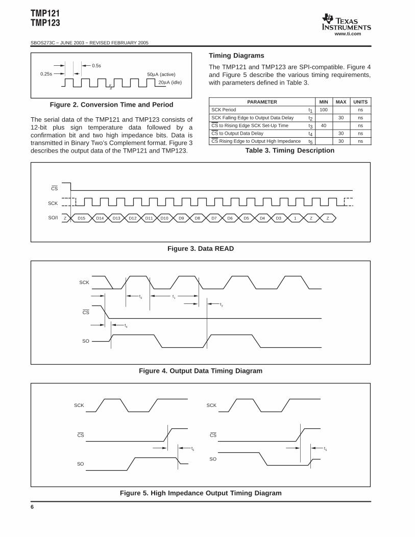
The serial data of the TMP121 and TMP123 consists of12-bit plus sign temperature data followed by aconfirmation bit and two high impedance bits. Data istransmitted in Binary Two’s Complement format. Figure 3describes the output data of the TMP121 and TMP123.
Timing Diagrams
The TMP121 and TMP123 are SPI-compatible. Figure 4and Figure 5 describe the various timing requirements,with parameters defined in Table 3.
PARAMETER MIN MAX UNITS
SCK Period t1 100 ns
SCK Falling Edge to Output Data Delay t2 30 ns
CS to Rising Edge SCK Set-Up Time t3 40 ns
CS to Output Data Delay t4 30 ns
CS Rising Edge to Output High Impedance t5 30 ns
Table 3. Timing Description
SO/I
SCK
CS
ZZ1D3D4D5D6D7D8D9D10D11D12D13D14D15Z
Figure 3. Data READ
SCK
CS
SO
t1t3
t2
t4
Figure 4. Output Data Timing Diagram
SCK
CS
SO
t5 t5
SCK
CS
SO
Figure 5. High Impedance Output Timing Diagram

PACKAGING INFORMATION
Orderable Device Status (1) PackageType
PackageDrawing
Pins PackageQty
Eco Plan (2) Lead/Ball Finish MSL Peak Temp (3)
TMP121AIDBVR ACTIVE SOT-23 DBV 6 3000 Green (RoHS &no Sb/Br)
CU NIPDAU Level-2-260C-1 YEAR
TMP121AIDBVRG4 ACTIVE SOT-23 DBV 6 3000 Green (RoHS &no Sb/Br)
CU NIPDAU Level-2-260C-1 YEAR
TMP121AIDBVT ACTIVE SOT-23 DBV 6 250 Green (RoHS &no Sb/Br)
CU NIPDAU Level-2-260C-1 YEAR
TMP121AIDBVTG4 ACTIVE SOT-23 DBV 6 250 Green (RoHS &no Sb/Br)
CU NIPDAU Level-2-260C-1 YEAR
TMP123AIDBVR ACTIVE SOT-23 DBV 6 3000 Green (RoHS &no Sb/Br)
CU NIPDAU Level-2-260C-1 YEAR
TMP123AIDBVRG4 ACTIVE SOT-23 DBV 6 3000 Green (RoHS &no Sb/Br)
CU NIPDAU Level-2-260C-1 YEAR
TMP123AIDBVT ACTIVE SOT-23 DBV 6 250 Green (RoHS &no Sb/Br)
CU NIPDAU Level-2-260C-1 YEAR
TMP123AIDBVTG4 ACTIVE SOT-23 DBV 6 250 Green (RoHS &no Sb/Br)
CU NIPDAU Level-2-260C-1 YEAR
(1) The marketing status values are defined as follows:ACTIVE: Product device recommended for new designs.LIFEBUY: TI has announced that the device will be discontinued, and a lifetime-buy period is in effect.NRND: Not recommended for new designs. Device is in production to support existing customers, but TI does not recommend using this part ina new design.PREVIEW: Device has been announced but is not in production. Samples may or may not be available.OBSOLETE: TI has discontinued the production of the device.
(2) Eco Plan - The planned eco-friendly classification: Pb-Free (RoHS), Pb-Free (RoHS Exempt), or Green (RoHS & no Sb/Br) - please checkhttp://www.ti.com/productcontent for the latest availability information and additional product content details.TBD: The Pb-Free/Green conversion plan has not been defined.Pb-Free (RoHS): TI's terms "Lead-Free" or "Pb-Free" mean semiconductor products that are compatible with the current RoHS requirementsfor all 6 substances, including the requirement that lead not exceed 0.1% by weight in homogeneous materials. Where designed to be solderedat high temperatures, TI Pb-Free products are suitable for use in specified lead-free processes.Pb-Free (RoHS Exempt): This component has a RoHS exemption for either 1) lead-based flip-chip solder bumps used between the die andpackage, or 2) lead-based die adhesive used between the die and leadframe. The component is otherwise considered Pb-Free (RoHScompatible) as defined above.Green (RoHS & no Sb/Br): TI defines "Green" to mean Pb-Free (RoHS compatible), and free of Bromine (Br) and Antimony (Sb) based flameretardants (Br or Sb do not exceed 0.1% by weight in homogeneous material)
(3) MSL, Peak Temp. -- The Moisture Sensitivity Level rating according to the JEDEC industry standard classifications, and peak soldertemperature.
Important Information and Disclaimer:The information provided on this page represents TI's knowledge and belief as of the date that it isprovided. TI bases its knowledge and belief on information provided by third parties, and makes no representation or warranty as to theaccuracy of such information. Efforts are underway to better integrate information from third parties. TI has taken and continues to takereasonable steps to provide representative and accurate information but may not have conducted destructive testing or chemical analysis onincoming materials and chemicals. TI and TI suppliers consider certain information to be proprietary, and thus CAS numbers and other limitedinformation may not be available for release.
In no event shall TI's liability arising out of such information exceed the total purchase price of the TI part(s) at issue in this document sold by TIto Customer on an annual basis.
OTHER QUALIFIED VERSIONS OF TMP121 :
• Enhanced Product: TMP121-EP
NOTE: Qualified Version Definitions:
PACKAGE OPTION ADDENDUM
www.ti.com 18-Sep-2008
Addendum-Page 1

• Enhanced Product - Supports Defense, Aerospace and Medical Applications
PACKAGE OPTION ADDENDUM
www.ti.com 18-Sep-2008
Addendum-Page 2

TAPE AND REEL INFORMATION
*All dimensions are nominal
Device PackageType
PackageDrawing
Pins SPQ ReelDiameter
(mm)
ReelWidth
W1 (mm)
A0 (mm) B0 (mm) K0 (mm) P1(mm)
W(mm)
Pin1Quadrant
TMP121AIDBVR SOT-23 DBV 6 3000 180.0 8.4 3.2 3.1 1.39 4.0 8.0 Q3
TMP121AIDBVT SOT-23 DBV 6 250 180.0 8.4 3.2 3.1 1.39 4.0 8.0 Q3
TMP123AIDBVR SOT-23 DBV 6 3000 180.0 8.4 3.2 3.1 1.39 4.0 8.0 Q3
TMP123AIDBVT SOT-23 DBV 6 250 180.0 8.4 3.2 3.1 1.39 4.0 8.0 Q3
PACKAGE MATERIALS INFORMATION
www.ti.com 11-Mar-2008
Pack Materials-Page 1
*All dimensions are nominal
Device Package Type Package Drawing Pins SPQ Length (mm) Width (mm) Height (mm)
TMP121AIDBVR SOT-23 DBV 6 3000 190.5 212.7 31.8
TMP121AIDBVT SOT-23 DBV 6 250 190.5 212.7 31.8
TMP123AIDBVR SOT-23 DBV 6 3000 190.5 212.7 31.8
TMP123AIDBVT SOT-23 DBV 6 250 190.5 212.7 31.8
PACKAGE MATERIALS INFORMATION
www.ti.com 11-Mar-2008
Pack Materials-Page 2


PACKAGE OPTION ADDENDUM
www.ti.com 10-Dec-2020
Addendum-Page 1
PACKAGING INFORMATION
Orderable Device Status(1)
Package Type PackageDrawing
Pins PackageQty
Eco Plan(2)
Lead finish/Ball material
(6)
MSL Peak Temp(3)
Op Temp (°C) Device Marking(4/5)
Samples
TMP121AIDBVR ACTIVE SOT-23 DBV 6 3000 RoHS & Green NIPDAU Level-2-260C-1 YEAR -40 to 125 T121
TMP121AIDBVRG4 ACTIVE SOT-23 DBV 6 3000 RoHS & Green NIPDAU Level-2-260C-1 YEAR -40 to 125 T121
TMP121AIDBVT ACTIVE SOT-23 DBV 6 250 RoHS & Green NIPDAU Level-2-260C-1 YEAR -40 to 125 T121
TMP121AIDBVTG4 ACTIVE SOT-23 DBV 6 250 RoHS & Green NIPDAU Level-2-260C-1 YEAR -40 to 125 T121
TMP123AIDBVR ACTIVE SOT-23 DBV 6 3000 RoHS & Green NIPDAU Level-2-260C-1 YEAR -55 to 125 T123
TMP123AIDBVRG4 ACTIVE SOT-23 DBV 6 3000 RoHS & Green NIPDAU Level-2-260C-1 YEAR -55 to 125 T123
TMP123AIDBVT ACTIVE SOT-23 DBV 6 250 RoHS & Green NIPDAU Level-2-260C-1 YEAR -55 to 125 T123
TMP123AIDBVTG4 ACTIVE SOT-23 DBV 6 250 RoHS & Green NIPDAU Level-2-260C-1 YEAR -55 to 125 T123
(1) The marketing status values are defined as follows:ACTIVE: Product device recommended for new designs.LIFEBUY: TI has announced that the device will be discontinued, and a lifetime-buy period is in effect.NRND: Not recommended for new designs. Device is in production to support existing customers, but TI does not recommend using this part in a new design.PREVIEW: Device has been announced but is not in production. Samples may or may not be available.OBSOLETE: TI has discontinued the production of the device.
(2) RoHS: TI defines "RoHS" to mean semiconductor products that are compliant with the current EU RoHS requirements for all 10 RoHS substances, including the requirement that RoHS substancedo not exceed 0.1% by weight in homogeneous materials. Where designed to be soldered at high temperatures, "RoHS" products are suitable for use in specified lead-free processes. TI mayreference these types of products as "Pb-Free".RoHS Exempt: TI defines "RoHS Exempt" to mean products that contain lead but are compliant with EU RoHS pursuant to a specific EU RoHS exemption.Green: TI defines "Green" to mean the content of Chlorine (Cl) and Bromine (Br) based flame retardants meet JS709B low halogen requirements of <=1000ppm threshold. Antimony trioxide basedflame retardants must also meet the <=1000ppm threshold requirement.
(3) MSL, Peak Temp. - The Moisture Sensitivity Level rating according to the JEDEC industry standard classifications, and peak solder temperature.
(4) There may be additional marking, which relates to the logo, the lot trace code information, or the environmental category on the device.
(5) Multiple Device Markings will be inside parentheses. Only one Device Marking contained in parentheses and separated by a "~" will appear on a device. If a line is indented then it is a continuationof the previous line and the two combined represent the entire Device Marking for that device.
PACKAGE OPTION ADDENDUM
www.ti.com 10-Dec-2020
Addendum-Page 2
(6) Lead finish/Ball material - Orderable Devices may have multiple material finish options. Finish options are separated by a vertical ruled line. Lead finish/Ball material values may wrap to twolines if the finish value exceeds the maximum column width.
Important Information and Disclaimer:The information provided on this page represents TI's knowledge and belief as of the date that it is provided. TI bases its knowledge and belief on informationprovided by third parties, and makes no representation or warranty as to the accuracy of such information. Efforts are underway to better integrate information from third parties. TI has taken andcontinues to take reasonable steps to provide representative and accurate information but may not have conducted destructive testing or chemical analysis on incoming materials and chemicals.TI and TI suppliers consider certain information to be proprietary, and thus CAS numbers and other limited information may not be available for release.
In no event shall TI's liability arising out of such information exceed the total purchase price of the TI part(s) at issue in this document sold by TI to Customer on an annual basis.
OTHER QUALIFIED VERSIONS OF TMP121 :
• Enhanced Product: TMP121-EP
NOTE: Qualified Version Definitions:
• Enhanced Product - Supports Defense, Aerospace and Medical Applications
TAPE AND REEL INFORMATION
*All dimensions are nominal
Device PackageType
PackageDrawing
Pins SPQ ReelDiameter
(mm)
ReelWidth
W1 (mm)
A0(mm)
B0(mm)
K0(mm)
P1(mm)
W(mm)
Pin1Quadrant
TMP121AIDBVR SOT-23 DBV 6 3000 178.0 9.0 3.23 3.17 1.37 4.0 8.0 Q3
TMP121AIDBVT SOT-23 DBV 6 250 178.0 9.0 3.23 3.17 1.37 4.0 8.0 Q3
TMP123AIDBVR SOT-23 DBV 6 3000 178.0 9.0 3.23 3.17 1.37 4.0 8.0 Q3
TMP123AIDBVT SOT-23 DBV 6 250 178.0 9.0 3.23 3.17 1.37 4.0 8.0 Q3
PACKAGE MATERIALS INFORMATION
www.ti.com 24-Apr-2020
Pack Materials-Page 1

*All dimensions are nominal
Device Package Type Package Drawing Pins SPQ Length (mm) Width (mm) Height (mm)
TMP121AIDBVR SOT-23 DBV 6 3000 180.0 180.0 18.0
TMP121AIDBVT SOT-23 DBV 6 250 180.0 180.0 18.0
TMP123AIDBVR SOT-23 DBV 6 3000 445.0 220.0 345.0
TMP123AIDBVT SOT-23 DBV 6 250 445.0 220.0 345.0
PACKAGE MATERIALS INFORMATION
www.ti.com 24-Apr-2020
Pack Materials-Page 2

www.ti.com
PACKAGE OUTLINE
C
0.220.08 TYP
0.25
3.02.6
2X 0.95
1.45 MAX
0.150.00 TYP
6X 0.500.25
0.60.3 TYP
80 TYP
1.9
A
3.052.75
B1.751.45
(1.1)
SOT-23 - 1.45 mm max heightDBV0006ASMALL OUTLINE TRANSISTOR
4214840/C 06/2021
NOTES: 1. All linear dimensions are in millimeters. Any dimensions in parenthesis are for reference only. Dimensioning and tolerancing per ASME Y14.5M.2. This drawing is subject to change without notice.3. Body dimensions do not include mold flash or protrusion. Mold flash and protrusion shall not exceed 0.25 per side.4. Leads 1,2,3 may be wider than leads 4,5,6 for package orientation.5. Refernce JEDEC MO-178.
0.2 C A B
1
34
52
INDEX AREAPIN 1
6
GAGE PLANE
SEATING PLANE
0.1 C
SCALE 4.000

www.ti.com
EXAMPLE BOARD LAYOUT
0.07 MAXARROUND
0.07 MINARROUND
6X (1.1)
6X (0.6)
(2.6)
2X (0.95)
(R0.05) TYP
4214840/C 06/2021
SOT-23 - 1.45 mm max heightDBV0006ASMALL OUTLINE TRANSISTOR
NOTES: (continued) 6. Publication IPC-7351 may have alternate designs. 7. Solder mask tolerances between and around signal pads can vary based on board fabrication site.
SYMM
LAND PATTERN EXAMPLEEXPOSED METAL SHOWN
SCALE:15X
PKG
1
3 4
52
6
SOLDER MASKOPENINGMETAL UNDER
SOLDER MASK
SOLDER MASKDEFINED
EXPOSED METAL
METALSOLDER MASKOPENING
NON SOLDER MASKDEFINED
(PREFERRED)
SOLDER MASK DETAILS
EXPOSED METAL
www.ti.com
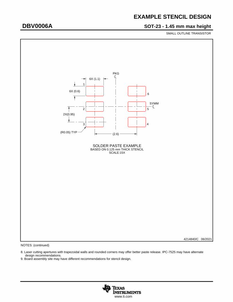
EXAMPLE STENCIL DESIGN
(2.6)
2X(0.95)
6X (1.1)
6X (0.6)
(R0.05) TYP
SOT-23 - 1.45 mm max heightDBV0006ASMALL OUTLINE TRANSISTOR
4214840/C 06/2021
NOTES: (continued) 8. Laser cutting apertures with trapezoidal walls and rounded corners may offer better paste release. IPC-7525 may have alternate design recommendations. 9. Board assembly site may have different recommendations for stencil design.
SOLDER PASTE EXAMPLEBASED ON 0.125 mm THICK STENCIL
SCALE:15X
SYMM
PKG
1
3 4
52
6

IMPORTANT NOTICE AND DISCLAIMERTI PROVIDES TECHNICAL AND RELIABILITY DATA (INCLUDING DATASHEETS), DESIGN RESOURCES (INCLUDING REFERENCEDESIGNS), APPLICATION OR OTHER DESIGN ADVICE, WEB TOOLS, SAFETY INFORMATION, AND OTHER RESOURCES “AS IS”AND WITH ALL FAULTS, AND DISCLAIMS ALL WARRANTIES, EXPRESS AND IMPLIED, INCLUDING WITHOUT LIMITATION ANYIMPLIED WARRANTIES OF MERCHANTABILITY, FITNESS FOR A PARTICULAR PURPOSE OR NON-INFRINGEMENT OF THIRDPARTY INTELLECTUAL PROPERTY RIGHTS.These resources are intended for skilled developers designing with TI products. You are solely responsible for (1) selecting the appropriateTI products for your application, (2) designing, validating and testing your application, and (3) ensuring your application meets applicablestandards, and any other safety, security, or other requirements. These resources are subject to change without notice. TI grants youpermission to use these resources only for development of an application that uses the TI products described in the resource. Otherreproduction and display of these resources is prohibited. No license is granted to any other TI intellectual property right or to any third partyintellectual property right. TI disclaims responsibility for, and you will fully indemnify TI and its representatives against, any claims, damages,costs, losses, and liabilities arising out of your use of these resources.TI’s products are provided subject to TI’s Terms of Sale (https:www.ti.com/legal/termsofsale.html) or other applicable terms available eitheron ti.com or provided in conjunction with such TI products. TI’s provision of these resources does not expand or otherwise alter TI’sapplicable warranties or warranty disclaimers for TI products.IMPORTANT NOTICE
Mailing Address: Texas Instruments, Post Office Box 655303, Dallas, Texas 75265Copyright © 2021, Texas Instruments Incorporated