top252-261 topswitch-hx family
TRANSCRIPT

TOP252-261
TOPSwitch-HX Family
www.powerint.com February 2008
Enhanced EcoSmart®, Integrated Off-Line Switcher with Advanced Feature Set and Extended Power Range
®
Product Highlights
Lower System Cost, Higher Design Flexibility
Multi-mode operation maximizes effi ciency at all loads
New eSIP-7C package builds on PI’s experience with high
power and high reliability packages
Low thermal impedance junction-to-case (2 °C per watt)
Low height is ideal for adapters where space is limited
Simple mounting using a clip to aid low cost manufacturing
No heatsink required up to 35 W using P, G and M packages
with universal input voltage and up to 48 W at 230 VAC
Output overvoltage protection (OVP) is user programmable for
latching/non-latching shutdown with fast AC reset
Allows both primary and secondary sensing
Line undervoltage (UV) detection prevents turn-off glitches
Line overvoltage (OV) shutdown extends line surge limit
Accurate programmable current limit
Optimized line feed-forward for line ripple rejection
132 kHz frequency (254Y-258Y and all E packages) reduces
transformer and power supply size
Half frequency option for video applications
Frequency jittering reduces EMI fi lter cost
Heatsink is connected to SOURCE for low EMI
Improved auto-restart delivers <3% of maximum power in short
circuit and open loop fault conditions
Accurate hysteretic thermal shutdown function automatically
recovers without requiring a reset
Fully integrated soft-start for minimum start-up stress
Extended creepage between DRAIN and all other pins improves
fi eld reliability
•
•
•
•
•
•
•
•
•
•
•
•
•
•
•
•
•
•
•
•
Figure 1. Typical Flyback Application.
EcoSmart®– Energy Effi cient
Energy effi cient over entire load range
No-load consumption
Less than 200 mW at 265 VAC for TOP256-258
Less than 300 mW at 265 VAC for TOP259-261
Standby power for 1 W input
>600 mW output at 110 VAC input
>500 mW output at 265 VAC input
Description
TOPSwitch-HX cost effectively incorporates a 700 V power
MOSFET, high voltage switched current source, PWM control,
oscillator, thermal shutdown circuit, fault protection and other
control circuitry onto a monolithic device.
•
•
•
•
•
•
•
PI-4510-100206
AC IN
DC OUT
D
S
C TOPSwitch-HX CONTROL
V
+
-
F X
Output Power Table
Product5
230 VAC ±15%4 85-265 VACProduct5
230 VAC ±15% 85-265 VAC
Adapter1 Open
Frame2 Peak3 Adapter1 Open
Frame2 Peak3 Adapter1 Open
Frame2 Adapter1 Open
Frame2
TOP252PN/GN9 W 15 W
21 W6.5 W 10 W
13 W TOP252EN 10 W 21 W 6 W 13 W
TOP252MN 21 W 13 WTOP253EN 21 W 43 W 13 W 29 W
TOP253PN/GN15 W 25 W
38 W9 W 15 W
25 W
TOP254EN/YN 30 W 62 W 20 W 43 WTOP253MN 43 W 29 W
TOP254PN/GN16 W 28 W
47 W11 W 20 W
30 W TOP255EN/YN 40 W 81 W 26 W 57 W
TOP254MN 62 W 40 WTOP256EN/YN 60 W 119 W 40 W 86 W
TOP255PN/GN19 W 30 W
54 W13 W 22 W
35 W
TOP257EN/YN 85 W 157 W 55 W 119 WTOP255MN 81 W 52 W
TOP258EN/YN 105 W 195 W 70 W 148 WTOP256PN/GN21 W 34 W
63 W15 W 26 W
40 W
TOP256MN 98 W 64 WTOP259EN/YN 128 W 238 W 80 W 171 W
TOP257PN/GN25 W 41 W
70 W19 W 30 W
45 WTOP260EN/YN 147 W 275 W 93 W 200 W
TOP257MN 119 W 78 W
TOP261EN/YN 177 W 333 W 118 W 254 WTOP258PN/GN29 W 48 W
77 W22 W 35 W
50 W
TOP258MN 140 W 92 W
Table 1. Output Power Table. (for notes see page 2).
Rev. B 02/08
2
TOP252-261
www.powerint.com
PI-4973-122607
ACIN
DCOUT
D
S
CTOPSwitch-HXCONTROL
V
+
-
GX
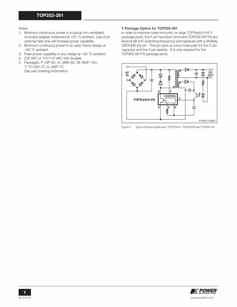
Figure 2. Typical Flyback Application TOP259YN, TOP260YN and TOP261YN.
Y Package Option for TOP259-261In order to improve noise-immunity on large TOPSwitch-HX Y
package parts, the F pin has been removed (TOP259-261YN are
fi xed at 66 kHz switching frequency) and replaced with a SIGNAL
GROUND (G) pin. This pin acts as a low noise path for the C pin
capacitor and the X pin resistor. It is only required for the
TOP259-261YN package parts.
Notes:
1. Minimum continuous power in a typical non-ventilated
enclosed adapter measured at +50 °C ambient. Use of an
external heat sink will increase power capability.
2. Minimum continuous power in an open frame design at
+50 °C ambient.
3. Peak power capability in any design at +50 °C ambient.
4. 230 VAC or 110/115 VAC with doubler.
5. Packages: P: DIP-8C, G: SMD-8C, M: SDIP-10C,
Y: TO-220-7C, E: eSIP-7C.
See part ordering information.

Rev. B 02/08
3
TOP252-261
www.powerint.com
Section List
Functional Block Diagram ....................................................................................................................................... 4
Pin Functional Description ...................................................................................................................................... 6
TOPSwitch-HX Family Functional Description ....................................................................................................... 7
CONTROL (C) Pin Operation .................................................................................................................................... 8
Oscillator and Switching Frequency .......................................................................................................................... 8
Pulse Width Modulator ............................................................................................................................................ 9
Maximum Load Cycle .............................................................................................................................................. 9
Error Amplifi er .......................................................................................................................................................... 9
On-Chip Current Limit with External Programmability ............................................................................................... 9
Line Under-Voltage Detection (UV) .......................................................................................................................... 10
Line Overvoltage Shutdown (OV) ............................................................................................................................ 11
Hysteretic or Latching Output Overvoltage Protection (OVP)................................................................................... 11
Line Feed-Forward with DCMAX
Reduction .............................................................................................................. 13
Remote ON/OFF and Synchronization .................................................................................................................... 13
Soft-Start ............................................................................................................................................................... 13
Shutdown/Auto-Restart ......................................................................................................................................... 13
Hysteretic Over-Temperature Protection ................................................................................................................. 13
Bandgap Reference ............................................................................................................................................... 13
High-Voltage Bias Current Source .......................................................................................................................... 13
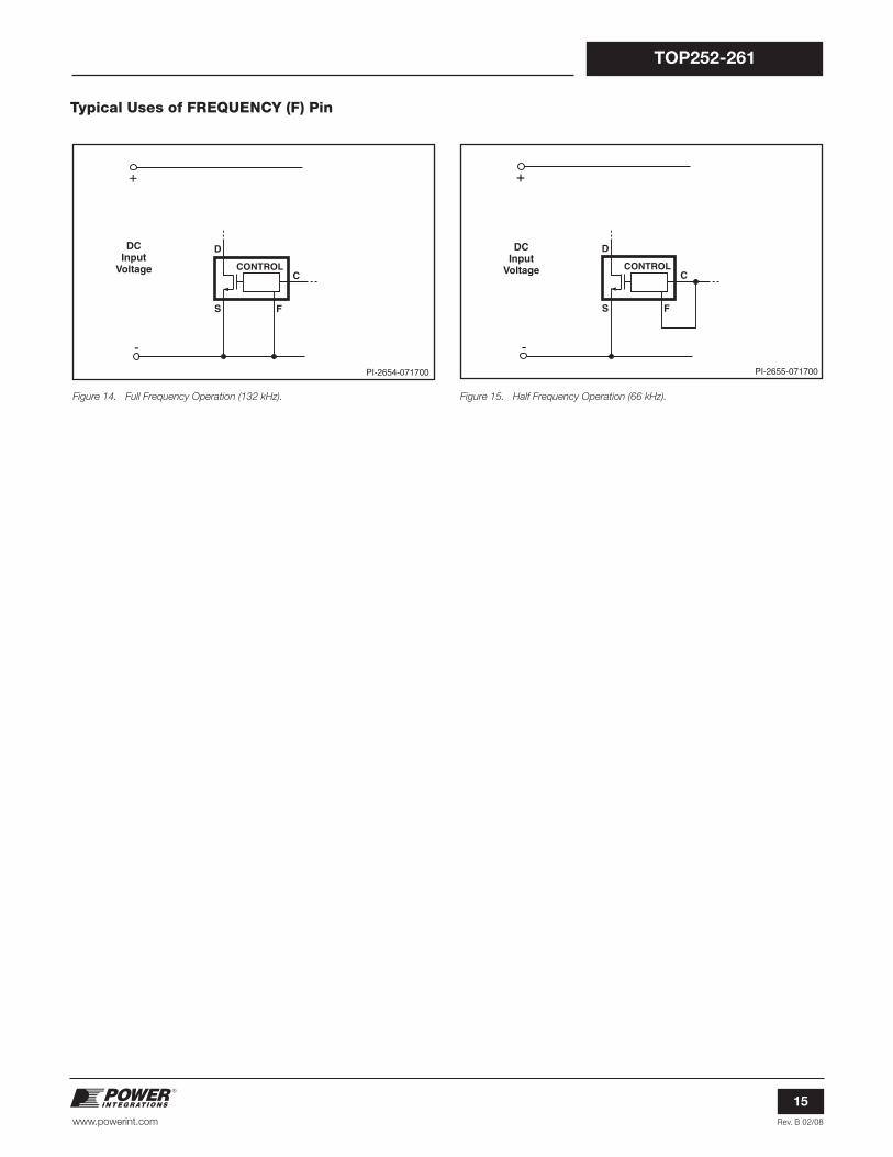
Typical Uses of FREQUENCY (F) Pin ...................................................................................................................... 15
Typical Uses of VOLTAGE MONITOR (V) and EXTERNAL CURRENT LIMIT (X) Pins .......................................... 16
Typical Uses of MULTI-FUNCTION (M) Pin ........................................................................................................... 18
Application Examples .............................................................................................................................................. 21
A High Effi ciency, 35 W, Dual Output – Universal Input Power Supply ..................................................................... 21
A High Effi ciency, 150 W, 250-380 VDC Input Power Supply .................................................................................. 22
A High Effi ciency, 20 W Continuous – 80 W Peak, Universal Input Power Supply ................................................... 23
A High Effi ciency, 65 W, Universal Input Power Supply ........................................................................................... 24
Key Application Considerations .............................................................................................................................. 25
TOPSwitch-HX vs.TOPSwitch-GX ....................................................................................................................... . 25
TOPSwitch-HX Design Considerations .................................................................................................................. 26
TOPSwitch-HX Layout Considerations ................................................................................................................... 27
Quick Design Checklist .......................................................................................................................................... 31
Design Tools .......................................................................................................................................................... 31
Product Specifi cations and Test Conditions .......................................................................................................... 32
Typical Performance Characteristics .................................................................................................................... 39
Package Outlines .................................................................................................................................................... 43
Part Ordering Information ........................................................................................................................................ 46

Rev. B 02/08
4
TOP252-261
www.powerint.com
Figure 3a. Functional Block Diagram (P and G Packages).
Figure 3b. Functional Block Diagram (M Package).
PI-4643-082907
SHUTDOWN/ AUTO-RESTART
CLOCK
CONTROLLED TURN-ON
GATE DRIVER
CURRENT LIMIT COMPARATOR
INTERNAL UV COMPARATOR
INTERNAL SUPPLY
5.8 V 4.8 V
SOURCE (S)
SOURCE (S)
S
R
Q
DMAX
STOP SOFT START
CONTROL (C)
VOLTAGE MONITOR (V)
-
+ 5.8 V
IFB
1 V
ZC
VC
+
-
+
-
+
-
LEADING EDGE
BLANKING
÷ 16
1
HYSTERETIC THERMAL
SHUTDOWN
SHUNT REGULATOR/ ERROR AMPLIFIER +
-
DRAIN (D)
ON/OFF
DCMAX
DCMAX
0
OV/ UV
OVP V
VI (LIMIT) CURRENT
LIMIT ADJUST
VBG + VT
LINE SENSE
SOFT START
OFF
F REDUCTION
F REDUCTION
STOP LOGIC
EXTERNAL CURRENT LIMIT (X)
OSCILLATOR WITH JITTER
PWM
KPS(UPPER)
KPS(LOWER)
SOFT START IFB
IPS(UPPER) IPS(LOWER)
KPS(UPPER)KPS(LOWER)
PI-4508-120307
SHUTDOWN/ AUTO-RESTART
CLOCK
CONTROLLED TURN-ON
GATE DRIVER
CURRENT LIMIT COMPARATOR
INTERNAL UV COMPARATOR
INTERNAL SUPPLY
5.8 V 4.8 V
KPS(UPPER)
KPS(LOWER)
SOURCE (S)
SOURCE (S)
S
R
Q
DMAX
STOP SOFT START
CONTROL (C)
MULTI- FUNCTION (M)
-
+ 5.8 V
IFB
ZC
VC
+
-
+
-
+
-
LEADING EDGE
BLANKING
÷ 16
1
HYSTERETIC THERMAL
SHUTDOWN
SHUNT REGULATOR/ ERROR AMPLIFIER +
-
DRAIN (D)
ON/OFF
DCMAX
DCMAX
0
OV/ UV
OVP V
VI (LIMIT) CURRENT
LIMIT ADJUST
VBG + VT
LINE SENSE
SOFT START
SOFT START IFB
IPS(UPPER) IPS(LOWER)
KPS(UPPER)KPS(LOWER)
OFF
F REDUCTION
F REDUCTION
STOP LOGIC
OSCILLATOR WITH JITTER
PWM

Rev. B 02/08
5
TOP252-261
www.powerint.com
Figure 3c. Functional Block Diagram (TOP254-258 Y Package and eSIP Package).
PI-4511-082907
SHUTDOWN/ AUTO-RESTART
CLOCK
CONTROLLED TURN-ON
GATE DRIVER
CURRENT LIMIT COMPARATOR
INTERNAL UV COMPARATOR
INTERNAL SUPPLY
5.8 V 4.8 V
SOURCE (S)
SOURCE (S)
S
R
Q
DMAX
STOP SOFT START
CONTROL (C)
VOLTAGE MONITOR (V)
FREQUENCY (F)
-
+ 5.8 V
IFB
1 V
ZC
VC
+
-
+
-
+
-
LEADING EDGE
BLANKING
÷ 16
1
HYSTERETIC THERMAL
SHUTDOWN
SHUNT REGULATOR/ ERROR AMPLIFIER +
-
DRAIN (D)
ON/OFF
DCMAX
DCMAX
66k/132k
0
OV/ UV
OVP V
VI (LIMIT) CURRENT
LIMIT ADJUST
VBG + VT
LINE SENSE
SOFT START
OFF
F REDUCTION
F REDUCTION
STOP LOGIC
EXTERNAL CURRENT LIMIT (X)
OSCILLATOR WITH JITTER
PWM
KPS(UPPER)
KPS(LOWER)
SOFT START IFB
IPS(UPPER) IPS(LOWER)
KPS(UPPER)KPS(LOWER)
PI-4974-122607
SHUTDOWN/ AUTO-RESTART
CLOCK
CONTROLLED TURN-ON
GATE DRIVER
CURRENT LIMIT COMPARATOR
INTERNAL UV COMPARATOR
INTERNAL SUPPLY
5.8 V 4.8 V
SIGNALGROUND (G)
SOURCE (S)
S
R
Q
DMAX
STOP SOFT START
CONTROL (C)
VOLTAGE MONITOR (V)
-
+ 5.8 V
IFB
1 V
ZC
VC
+
-
+
-
+
-
LEADING EDGE
BLANKING
÷ 16
1
HYSTERETIC THERMAL
SHUTDOWN
SHUNT REGULATOR/ ERROR AMPLIFIER +
-
DRAIN (D)
SOURCE (S)
ON/OFF
DCMAX
DCMAX
0
OV/ UV
OVP V
VI (LIMIT) CURRENT
LIMIT ADJUST
VBG + VT
LINE SENSE
SOFT START
OFF
F REDUCTION
F REDUCTION
STOP LOGIC
EXTERNAL CURRENT LIMIT (X)
OSCILLATOR WITH JITTER
PWM
KPS(UPPER)
KPS(LOWER)
SOFT START IFB
IPS(UPPER) IPS(LOWER)
KPS(UPPER)KPS(LOWER)
Figure 3d. Functional Block Diagram TOP259YN, TOP260YN, TOP261YN.
Rev. B 02/08
6
TOP252-261
www.powerint.com
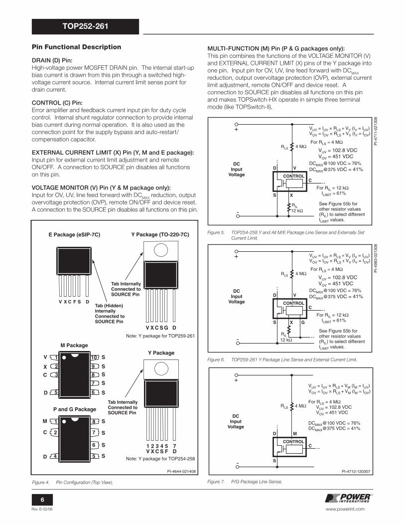
Pin Functional Description
DRAIN (D) Pin:High-voltage power MOSFET DRAIN pin. The internal start-up
bias current is drawn from this pin through a switched high-
voltage current source. Internal current limit sense point for
drain current.
CONTROL (C) Pin:Error amplifi er and feedback current input pin for duty cycle
control. Internal shunt regulator connection to provide internal
bias current during normal operation. It is also used as the
connection point for the supply bypass and auto-restart/
compensation capacitor.
EXTERNAL CURRENT LIMIT (X) Pin (Y, M and E package):Input pin for external current limit adjustment and remote
ON/OFF. A connection to SOURCE pin disables all functions
on this pin.
VOLTAGE MONITOR (V) Pin (Y & M package only):Input for OV, UV, line feed forward with DC
MAX reduction, output
overvoltage protection (OVP), remote ON/OFF and device reset.
A connection to the SOURCE pin disables all functions on this pin.
Figure 4. Pin Confi guration (Top View).
X
PI-
4711
-021
308
DCInput
Voltage
+
-
D
S
CCONTROL
V
RIL
RLS
12 k
4 M
VUV = IUV × RLS + VV (IV = IUV)VOV = IOV × RLS + VV (IV = IOV)
For RLS = 4 M
DCMAX@100 VDC = 76%DCMAX@375 VDC = 41%
For RIL = 12 k ILIMIT = 61%
See Figure 55b for other resistor values (RIL) to select different ILIMIT values.
VUV = 102.8 VDC VOV = 451 VDC
Figure 5. TOP254-258 Y and All M/E Package Line Sense and Externally Set
Current Limit.
PI-4712-120307
DCInput
Voltage
+
-
D M
S
C
VUV = IUV × RLS + VM (IM = IUV)VOV = IOV × RLS + VM (IM = IOV)
For RLS = 4 M VUV = 102.8 VDC VOV = 451 VDC
DCMAX@100 VDC = 76%DCMAX@375 VDC = 41%
CONTROL
RLS 4 M
Figure 7. P/G Package Line Sense.
PI-4644-021408
Tab InternallyConnected to SOURCE Pin
Tab InternallyConnected to SOURCE Pin
Tab (Hidden) InternallyConnected to SOURCE Pin
Y Package
D
C S
S
S
S
S
S
S
S
S
7D
5F
4S
3C
2X
1V
M
P and G Package
M Package
8
5
7
1
4
2
6
D
X
C
V 10
6
9
1
5
8
7
2
3
Note: Y package for TOP259-261
Note: Y package for TOP254-258
E Package (eSIP-7C) Y Package (TO-220-7C)
DGSCXV
V X C F S D
X G
PI-
4983
-021
308
DCInput
Voltage
+
-
D
S
CCONTROL
V
RIL
RLS
12 k
4 M
VUV = IUV × RLS + VV (IV = IUV)VOV = IOV × RLS + VV (IV = IOV)
For RLS = 4 M
DCMAX@100 VDC = 76%DCMAX@375 VDC = 41%
For RIL = 12 k ILIMIT = 61%
See Figure 55b for other resistor values (RIL) to select different ILIMIT values.
VUV = 102.8 VDC VOV = 451 VDC
Figure 6. TOP259-261 Y Package Line Sense and External Current Limit.
MULTI-FUNCTION (M) Pin (P & G packages only):This pin combines the functions of the VOLTAGE MONITOR (V)
and EXTERNAL CURRENT LIMIT (X) pins of the Y package into
one pin. Input pin for OV, UV, line feed forward with DCMAX
reduction, output overvoltage protection (OVP), external current
limit adjustment, remote ON/OFF and device reset. A
connection to SOURCE pin disables all functions on this pin
and makes TOPSwitch-HX operate in simple three terminal
mode (like TOPSwitch-II).

Rev. B 02/08
7
TOP252-261
www.powerint.com
PI-4713-021308
DCInput
Voltage
+
-
D M
S
C
For RIL = 12 k ILIMIT = 61%
CONTROLRIL
See Figure 55b for other resistor values (RIL) to select different ILIMIT values.
For RIL = 19 k ILIMIT = 37%
Figure 8. P/G Package Externally Set Current Limit.
FREQUENCY (F) Pin (TOP254-258 Y package & E packages):Input pin for selecting switching frequency 132 kHz if connected
to SOURCE pin and 66 kHz if connected to CONTROL pin.
The switching frequency is internally set for fi xed 66 kHz
operation in the P, G, M package and TOP259YN, TOP260YN
and TOP261YN.
SIGNAL GROUND (G) Pin (TOP259YN, TOP260YN & TOP261YN only):Return for C pin capacitor and X pin resistor.
SOURCE (S) Pin:Output MOSFET source connection for high voltage power
return. Primary side control circuit common and reference point.
TOPSwitch-HX Family Functional Description
Like TOPSwitch-GX, TOPSwitch-HX is an integrated switched
mode power supply chip that converts a current at the control
input to a duty cycle at the open drain output of a high voltage
power MOSFET. During normal operation the duty cycle of the
power MOSFET decreases linearly with increasing CONTROL
pin current as shown in Figure 9.
In addition to the three terminal TOPSwitch features, such as
the high voltage start-up, the cycle-by-cycle current limiting,
loop compensation circuitry, auto-restart and thermal
shutdown, the TOPSwitch-HX incorporates many additional
functions that reduce system cost, increase power supply
performance and design fl exibility. A patented high voltage
CMOS technology allows both the high-voltage power MOSFET
and all the low voltage control circuitry to be cost effectively
integrated onto a single monolithic chip.
Three terminals, FREQUENCY, VOLTAGE-MONITOR, and
EXTERNAL CURRENT LIMIT (available in Y and E packages),
two terminals, VOLTAGE-MONITOR and EXTERNAL CURRENT
LIMIT (available in M package) or one terminal MULTI-
FUNCTION (available in P and G package) have been used to
implement some of the new functions. These terminals can be
connected to the SOURCE pin to operate the TOPSwitch-HX in
a TOPSwitch-like three terminal mode. However, even in this
three terminal mode, the TOPSwitch-HX offers many
transparent features that do not require any external
components:
A fully integrated 17 ms soft-start signifi cantly reduces or
eliminates output overshoot in most applications by sweeping
both current limit and frequency from low to high to limit the
peak currents and voltages during start-up.
A maximum duty cycle (DCMAX
) of 78% allows smaller input
storage capacitor, lower input voltage requirement and/or
higher power capability.
Multi-mode operation optimizes and improves the power
supply effi ciency over the entire load range while maintaining
good cross regulation in multi-output supplies.
Switching frequency of 132 kHz reduces the transformer size
with no noticeable impact on EMI.
Frequency jittering reduces EMI in the full frequency mode at
high load condition.
1.
2.
3.
4.
5.
Figure 9. Control Pin Characteristics (Multi-Mode Operation).
PI-4645-041107
Du
ty C
ycle
(%
) D
rain
Pea
k C
urr
ent
To C
urr
ent
Lim
it R
atio
(%
) F
req
uen
cy (
kHz)
CONTROL Current
CONTROL Current
CONTROLCurrent
ICOFFIC03IC02 IC01 IB ICD1
100
78
55
25
132
66
30
Slope = PWM Gain (constant over load range)
Auto-Restart
Variable Frequency
Mode
Low Frequency
Mode
Multi-Cycle Modulation
Jitter
Full Frequency Mode

Rev. B 02/08
8
TOP252-261
www.powerint.com
Hysteretic over-temperature shutdown ensures automatic
recovery from thermal fault. Large hysteresis prevents circuit
board overheating.
Packages with omitted pins and lead forming provide large
drain creepage distance.
Reduction of the auto-restart duty cycle and frequency to
improve the protection of the power supply and load during
open loop fault, short circuit, or loss of regulation.
Tighter tolerances on I2f power coeffi cient, current limit
reduction, PWM gain and thermal shutdown threshold.
The VOLTAGE-MONITOR (V) pin is usually used for line sensing
by connecting a 4 MΩ resistor from this pin to the rectifi ed DC
high voltage bus to implement line overvoltage (OV), under-
voltage (UV) and dual-slope line feed-forward with DCMAX
reduction. In this mode, the value of the resistor determines the
OV/UV thresholds and the DCMAX
is reduced linearly with a dual
slope to improve line ripple rejection. In addition, it also
provides another threshold to implement the latched and
hysteretic output overvoltage protection (OVP). The pin can
also be used as a remote ON/OFF using the IUV
threshold.
The EXTERNAL CURRENT LIMIT (X) pin can be used to reduce
the current limit externally to a value close to the operating peak
current, by connecting the pin to SOURCE through a resistor.
This pin can also be used as a remote ON/OFF input.
For the P and G package the VOLTAGE-MONITOR and
EXTERNAL CURRENT LIMIT pin functions are combined on
one MULTI-FUNCTION (M) pin. However, some of the functions
become mutually exclusive.
The FREQUENCY (F) pin in the TOP254-258 Y and E packages
set the switching frequency in the full frequency PWM mode to
the default value of 132 kHz when connected to SOURCE pin.
A half frequency option of 66 kHz can be chosen by connecting
this pin to the CONTROL pin instead. Leaving this pin open is
not recommended. In the P, G and M packages and the
TOP259-261 Y packages, the frequency is set internally at
66 kHz in the full frequency PWM mode.
CONTROL (C) Pin OperationThe CONTROL pin is a low impedance node that is capable of
receiving a combined supply and feedback current. During
normal operation, a shunt regulator is used to separate the
feedback signal from the supply current. CONTROL pin voltage
VC is the supply voltage for the control circuitry including the
MOSFET gate driver. An external bypass capacitor closely
connected between the CONTROL and SOURCE pins is
required to supply the instantaneous gate drive current. The
total amount of capacitance connected to this pin also sets the
auto-restart timing as well as control loop compensation.
When rectifi ed DC high voltage is applied to the DRAIN pin
during start-up, the MOSFET is initially off, and the CONTROL
pin capacitor is charged through a switched high voltage
current source connected internally between the DRAIN and
CONTROL pins. When the CONTROL pin voltage VC reaches
approximately 5.8 V, the control circuitry is activated and the
soft-start begins. The soft-start circuit gradually increases the
6.
7.
8.
9.
drain peak current and switching frequency from a low starting
value to the maximum drain peak current at the full frequency
over approximately 17 ms. If no external feedback/supply
current is fed into the CONTROL pin by the end of the soft-start,
the high voltage current source is turned off and the CONTROL
pin will start discharging in response to the supply current
drawn by the control circuitry. If the power supply is designed
properly, and no fault condition such as open loop or shorted
output exists, the feedback loop will close, providing external
CONTROL pin current, before the CONTROL pin voltage has
had a chance to discharge to the lower threshold voltage of
approximately 4.8 V (internal supply undervoltage lockout
threshold). When the externally fed current charges the
CONTROL pin to the shunt regulator voltage of 5.8 V, current in
excess of the consumption of the chip is shunted to SOURCE
through an NMOS current mirror as shown in Figure 3. The
output current of that NMOS current mirror controls the duty
cycle of the power MOSFET to provide closed loop regulation.
The shunt regulator has a fi nite low output impedance ZC that
sets the gain of the error amplifi er when used in a primary
feedback confi guration. The dynamic impedance ZC of the
CONTROL pin together with the external CONTROL pin
capacitance sets the dominant pole for the control loop.
When a fault condition such as an open loop or shorted output
prevents the fl ow of an external current into the CONTROL pin,
the capacitor on the CONTROL pin discharges towards 4.8 V.
At 4.8 V, auto-restart is activated, which turns the output
MOSFET off and puts the control circuitry in a low current
standby mode. The high-voltage current source turns on and
charges the external capacitance again. A hysteretic internal
supply undervoltage comparator keeps VC within a window of
typically 4.8 V to 5.8 V by turning the high-voltage current
source on and off as shown in Figure 11. The auto-restart
circuit has a divide-by-sixteen counter, which prevents the
output MOSFET from turning on again until sixteen discharge/
charge cycles have elapsed. This is accomplished by enabling
the output MOSFET only when the divide-by-sixteen counter
reaches the full count (S15). The counter effectively limits
TOPSwitch-HX power dissipation by reducing the auto-restart
duty cycle to typically 2%. Auto-restart mode continues until
output voltage regulation is again achieved through closure of
the feedback loop.
Oscillator and Switching FrequencyThe internal oscillator linearly charges and discharges an
internal capacitance between two voltage levels to create a
triangular waveform for the timing of the pulse width modulator.
This oscillator sets the pulse width modulator/current limit latch
at the beginning of each cycle.
The nominal full switching frequency of 132 kHz was chosen to
minimize transformer size while keeping the fundamental EMI
frequency below 150 kHz. The FREQUENCY pin (available only
in TOP254-258 Y and E packages), when shorted to the
CONTROL pin, lowers the full switching frequency to 66 kHz
(half frequency), which may be preferable in some cases such
as noise sensitive video applications or a high effi ciency standby
mode. Otherwise, the FREQUENCY pin should be connected
to the SOURCE pin for the default 132 kHz. In the M, P and G

Rev. B 02/08
9
TOP252-261
www.powerint.com
Figure 10. Switching Frequency Jitter (Idealized VDRAIN
Waveforms).
PI-
4530
-041
107
fOSC -
4 ms
Time
Switching Frequency
VDRAIN
fOSC +
packages and the TOP259-261 Y package option, the full
frequency PWM mode is set at 66 kHz, for higher effi ciency and
increased output power in all applications.
To further reduce the EMI level, the switching frequency in the
full frequency PWM mode is jittered (frequency modulated) by
approximately ±2.5 kHz for 66 kHz operation or ±5 kHz for
132 kHz operation at a 250 Hz (typical) rate as shown in
Figure 10. The jitter is turned off gradually as the system is
entering the variable frequency mode with a fi xed peak drain
current.
Pulse Width ModulatorThe pulse width modulator implements multi-mode control by
driving the output MOSFET with a duty cycle inversely
proportional to the current into the CONTROL pin that is in
excess of the internal supply current of the chip (see Figure 9).
The feedback error signal, in the form of the excess current, is
fi ltered by an RC network with a typical corner frequency of
7 kHz to reduce the effect of switching noise in the chip supply
current generated by the MOSFET gate driver.
To optimize power supply effi ciency, four different control
modes are implemented. At maximum load, the modulator
operates in full frequency PWM mode; as load decreases, the
modulator automatically transitions, fi rst to variable frequency
PWM mode, then to low frequency PWM mode. At light load,
the control operation switches from PWM control to multi-cycle-
modulation control, and the modulator operates in multi-cycle-
modulation mode. Although different modes operate differently
to make transitions between modes smooth, the simple
relationship between duty cycle and excess CONTROL pin
current shown in Figure 9 is maintained through all three PWM
modes. Please see the following sections for the details of the
operation of each mode and the transitions between modes.
Full Frequency PWM mode: The PWM modulator enters full
frequency PWM mode when the CONTROL pin current (IC)
reaches IB. In this mode, the average switching frequency is
kept constant at fOSC
(66 kHz for P, G and M packages and
TOP259-261 Y, pin selectable 132 kHz or 66 kHz for Y and E
packages). Duty cycle is reduced from DCMAX
through the
reduction of the on-time when IC is increased beyond I
B. This
operation is identical to the PWM control of all other TOPSwitch
families. TOPSwitch-HX only operates in this mode if the cycle-
by-cycle peak drain current stays above kPS(UPPER)
*ILIMIT
(set),
where kPS(UPPER)
is 55% (typical) and ILIMIT
(set) is the current limit
externally set via the X or M pin.
Variable Frequency PWM mode: When peak drain current is
lowered to kPS(UPPER)
* ILIMIT
(set) as a result of power supply load
reduction, the PWM modulator initiates the transition to variable
frequency PWM mode, and gradually turns off frequency jitter.
In this mode, peak drain current is held constant at kPS(UPPER)
*
ILIMIT
(set) while switching frequency drops from the initial full
frequency of fOSC
(132 kHz or 66 kHz) towards the minimum
frequency of fMCM(MIN)
(30 kHz typical). Duty cycle reduction is
accomplished by extending the off-time.
Low Frequency PWM mode: When switching frequency
reaches fMCM(MIN)
(30 kHz typical), the PWM modulator starts to
transition to low frequency mode. In this mode, switching
frequency is held constant at fMCM(MIN)
and duty cycle is reduced,
similar to the full frequency PWM mode, through the reduction
of the on-time. Peak drain current decreases from the initial
value of kPS(UPPER)
* ILIMIT
(set) towards the minimum value of
kPS(LOWER)
*ILIMIT
(set), where kPS(LOWER)
is 25% (typical) and ILIMIT
(set) is
the current limit externally set via the X or M pin.
Multi-Cycle-Modulation mode: When peak drain current is
lowered to kPS(LOWER)
*ILIMIT
(set), the modulator transitions to multi-
cycle-modulation mode. In this mode, at each turn-on, the
modulator enables output switching for a period of TMCM(MIN)
at
the switching frequency of fMCM(MIN)
(4 or 5 consecutive pulses at
30 kHz) with the peak drain current of kPS(LOWER)
*ILIMIT
(set), and
stays off until the CONTROL pin current falls below IC(OFF)
. This
mode of operation not only keeps peak drain current low but
also minimizes harmonic frequencies between 6 kHz and
30 kHz. By avoiding transformer resonant frequency this way,
all potential transformer audible noises are greatly supressed.
Maximum Duty CycleThe maximum duty cycle, DC
MAX, is set at a default maximum
value of 78% (typical). However, by connecting the VOLTAGE-
MONITOR or MULTI-FUNCTION pin (depending on the
package) to the rectifi ed DC high voltage bus through a resistor
with appropriate value (4 MΩ typical), the maximum duty cycle
can be made to decrease from 78% to 40% (typical) when input
line voltage increases from 88 V to 380 V, with dual gain slopes.
Error Amplifi erThe shunt regulator can also perform the function of an error
amplifi er in primary side feedback applications. The shunt
regulator voltage is accurately derived from a temperature-
compensated bandgap reference. The CONTROL pin dynamic
impedance ZC sets the gain of the error amplifi er. The
CONTROL pin clamps external circuit signals to the VC voltage
level. The CONTROL pin current in excess of the supply
current is separated by the shunt regulator and becomes the
feedback current Ifb for the pulse width modulator.
On-Chip Current Limit with External Programmability The cycle-by-cycle peak drain current limit circuit uses the
output MOSFET ON-resistance as a sense resistor. A current
limit comparator compares the output MOSFET on-state drain

Rev. B 02/08
10
TOP252-261
www.powerint.com
to source voltage VDS(ON)
with a threshold voltage. High drain
current causes VDS(ON)
to exceed the threshold voltage and turns
the output MOSFET off until the start of the next clock cycle.
The current limit comparator threshold voltage is temperature
compensated to minimize the variation of the current limit due
to temperature related changes in RDS(ON)
of the output MOSFET.
The default current limit of TOPSwitch-HX is preset internally.
However, with a resistor connected between EXTERNAL
CURRENT LIMIT (X) pin (Y, E and M packages) or MULTI-
FUNCTION (M) pin (P and G package) and SOURCE pin (for
TOP259-261 Y, the X pin is connected to the SIGNAL GROUND
(G) pin), current limit can be programmed externally to a lower
level between 30% and 100% of the default current limit. By
setting current limit low, a larger TOPSwitch-HX than necessary
for the power required can be used to take advantage of the
lower RDS(ON)
for higher effi ciency/smaller heat sinking
requirements. TOPSwitch-HX current limit reduction initial
tolerance through the X pin (or M pin) has been improved
signifi cantly compare with previous TOPSwitch-GX. With a
second resistor connected between the EXTERNAL CURRENT
LIMIT (X) pin (Y, E and M packages) or MULTI-FUNCTION (M)
pin (P and G package) and the rectifi ed DC high voltage bus,
the current limit is reduced with increasing line voltage, allowing
a true power limiting operation against line variation to be
implemented. When using an RCD clamp, this power limiting
technique reduces maximum clamp voltage at high line. This
allows for higher refl ected voltage designs as well as reducing
clamp dissipation.
The leading edge blanking circuit inhibits the current limit
comparator for a short time after the output MOSFET is turned
on. The leading edge blanking time has been set so that, if a
power supply is designed properly, current spikes caused by
primary-side capacitances and secondary-side rectifi er reverse
recovery time should not cause premature termination of the
switching pulse.
The current limit is lower for a short period after the leading
edge blanking time. This is due to dynamic characteristics of
the MOSFET. During startup and fault conditions the controller
prevents excessive drain currents by reducing the switching
frequency.
Line Undervoltage Detection (UV)At power up, UV keeps TOPSwitch-HX off until the input line
voltage reaches the undervoltage threshold. At power down,
UV prevents auto-restart attempts after the output goes out of
regulation. This eliminates power down glitches caused by slow
discharge of the large input storage capacitor present in
applications such as standby supplies. A single resistor
connected from the VOLTAGE-MONITOR pin (Y, E and M
packages) or MULTI-FUNCTION pin (P and G packages) to the
rectifi ed DC high voltage bus sets UV threshold during power
up. Once the power supply is successfully turned on, the UV
threshold is lowered to 44% of the initial UV threshold to allow
extended input voltage operating range (UV low threshold). If
the UV low threshold is reached during operation without the
power supply losing regulation, the device will turn off and stay
off until UV (high threshold) has been reached again. If the
power supply loses regulation before reaching the UV low
threshold, the device will enter auto-restart. At the end of each
auto-restart cycle (S15), the UV comparator is enabled. If the
UV high threshold is not exceeded, the MOSFET will be
disabled during the next cycle (see Figure 11). The UV feature
can be disabled independent of the OV feature.
Line Overvoltage Shutdown (OV)The same resistor used for UV also sets an overvoltage
PI-4531-121206
S13 S12 S0 S15 S13 S12 S0 S15 S14 S13 S15S14 S14 5.8 V 4.8 V
S15
0 V
0 V
0 V
VLINE
VC
VDRAIN
VOUT
Note: S0 through S15 are the output states of the auto-restart counter
2 1 2 3 4
0 V
~ ~
~ ~
~ ~
~ ~
~ ~
S0 S15
~ ~
~ ~
~ ~
~ ~
VUV
~ ~
~ ~
~ ~
~ ~
S12 ~ ~
Figure 11. Typical Waveforms for (1) Power Up (2) Normal Operation (3) Auto-Restart (4) Power Down.

Rev. B 02/08
11
TOP252-261
www.powerint.com
threshold, which, once exceeded, will force TOPSwitch-HX to
stop switching instantaneously (after completion of the current
switching cycle). If this condition lasts for at least 100 μs, the
TOPSwitch-HX output will be forced into off state. Unlike with
TOPSwitch-GX, however, when the line voltage is back to
normal with a small amount of hysteresis provided on the OV
threshold to prevent noise triggering, the state machine sets to
S13 and forces TOPSwitch-HX to go through the entire auto-
restart sequence before attempting to switch again. The ratio
of OV and UV thresholds is preset at 4.5, as can be seen in
Figure 12. When the MOSFET is off, the rectifi ed DC high
voltage surge capability is increased to the voltage rating of the
MOSFET (700 V), due to the absence of the refl ected voltage
and leakage spikes on the drain. The OV feature can be
disabled independent of the UV feature.
In order to reduce the no-load input power of TOPSwitch-HX
designs, the V-pin (or M-pin for P Package) operates at very low
currents. This requires careful layout considerations when
designing the PCB to avoid noise coupling. Traces and
components connected to the V-pin should not be adjacent to
any traces carrying switching currents. These include the drain,
clamp network, bias winding return or power traces from other
converters. If the line sensing features are used, then the sense
resistors must be placed within 10 mm of the V-pin to minimize
the V-pin node area. The DC bus should then be routed to the
line sense resistors. Note that external capacitance must not
be connected to the V-pin as this may cause misoperaton of the
V pin related functions.
Hysteretic or Latching Output Overvoltage Protection (OVP)The detection of the hysteretic or latching output overvoltage
protection (OVP) is through the trigger of the line overvoltage
threshold. The V-pin or M-pin voltage will drop by 0.5 V, and
the controller measures the external attached impedance
immediately after this voltage drops. If IV or I
M exceeds I
OV(LS)
(336 μA typical) longer than 100 μs, TOPSwitch-HX will latch
into a permanent off state for the latching OVP. It only can be
reset if VV or V
M goes below 1 V or V
C goes below the power-
up-reset threshold (VC(RESET)
) and then back to normal.
If IV or I
M does not exceed I
OV(LS) or exceeds no longer than
100 μs, TOPSwitch-HX will initiate the line overvoltage and the
hysteretic OVP. Their behavior will be identical to the line
overvoltage shutdown (OV) that has been described in detail in
the previous section.
Voltage Monitor and External Current Limit Pin Table*
Figure Number 16 17 18 19 20 21 22 23 24 25 26 27 28
Three Terminal Operation ✓
Line Undervoltage ✓ ✓ ✓ ✓ ✓ ✓
Line Overvoltage ✓ ✓ ✓ ✓ ✓ ✓
Line Feed-Forward (DCMAX
) ✓ ✓ ✓ ✓ ✓
Output Overvoltage Protection ✓ ✓
Overload Power Limiting ✓
External Current Limit ✓ ✓ ✓ ✓ ✓
Remote ON/OFF ✓ ✓ ✓
Device Reset ✓
*This table is only a partial list of many VOLTAGE MONITOR and EXTERNAL CURRENT LIMIT Pin Confi gurations that are possible.
Table 2. VOLTAGE MONITOR (V) Pin and EXTERNAL CURRENT LIMIT (X) Pin Confi guration Options.
Multi-Function Pin Table*
Figure Number 29 30 31 32 33 34 35 36 37 38 39 40
Three Terminal Operation ✓
Line Undervoltage ✓ ✓ ✓ ✓
Line Overvoltage ✓ ✓ ✓ ✓
Line Feed-Forward (DCMAX
) ✓ ✓ ✓
Output Overvoltage Protection ✓ ✓
Overload Power Limiting ✓
External Current Limit ✓ ✓ ✓ ✓
Remote ON/OFF ✓ ✓ ✓
Device Reset ✓
*This table is only a partial list of many MULTI-FUNCTIONAL Pin Confi gurations that are possible.
Table 3. MULTI-FUNCTION (M) Pin Confi guration Options.

Rev. B 02/08
12
TOP252-261
www.powerint.com
Figure 12. MULTI-FUNCTION (P and G package). VOLTAGE MONITOR and EXTERNAL CURRENT LIMIT (Y, E and M package) Pin Characteristics.
-250 -200 -150 -100 -50 0 25 50 75 100 125 336
PI-4646-010908
Output MOSFET Switching
(Enabled)
(Disabled)
(Non-Latching) (Latching)
ILIMIT (Default)
DCMAX (78%)
Current Limit
M Pin
V Pin X Pin
Maximum Duty Cycle
VBG
I
I
I
I
IUV IREM(N) IOV IOV(LS)
Pin Voltage
Note: This figure provides idealized functional characteristics with typical performance values. Please refer to the parametric table and typical performance characteristics sections of the data sheet for measured data. For a detailed description of each functional pin operation refer to the Functional Description section of the data sheet.
X and V Pins (Y, E and M Packages) and M Pin (P and G Packages) Current (μA)
Disabled when supply output goes out of regulation
The circuit examples shown in Figures 41, 42 and 43 show a
simple method for implementing the primary sensed over-
voltage protection.
During a fault condition resulting from loss of feedback, output
voltage will rapidly rise above the nominal voltage. The increase
in output voltage will also result in an increase in the voltage at
the output of the bias winding. A voltage at the output of the
bias winding that exceeds of the sum of the voltage rating of the
Zener diode connected from the bias winding output to the
V-pin (or M-pin) and V-pin (or M-pin) voltage, will cause a
current in excess of IV or I
M to be injected into the V-pin
(or M-pin), which will trigger the OVP feature.
The primary sensed OVP protection circuit shown in Figures 41,
42 and 43 is triggered by a signifi cant rise in output voltage (and
therefore bias winding voltage). If the power supply is operating
under heavy load or low input line conditions when an open
loop occurs, the output voltage may not rise signifi cantly.
Under these conditions, a latching shutdown will not occur until
load or line conditions change. Nevertheless, the operation
provides the desired protection by preventing signifi cant rise in
the output voltage when the line or load conditions do change.
Primary side OVP protection with the TOPSwitch-HX in a typical
application will prevent a nominal 12 V output from rising above
approximately 20 V under open loop conditions. If greater
accuracy is required, a secondary sensed OVP circuit is
recommended.
Rev. B 02/08
13
TOP252-261
www.powerint.com
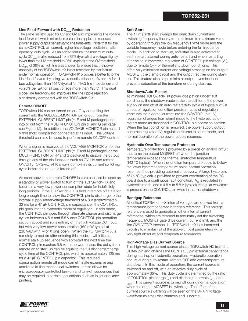
Line Feed-Forward with DCMAX ReductionThe same resistor used for UV and OV also implements line voltage
feed-forward, which minimizes output line ripple and reduces
power supply output sensitivity to line transients. Note that for the
same CONTROL pin current, higher line voltage results in smaller
operating duty cycle. As an added feature, the maximum duty
cycle DCMAX
is also reduced from 78% (typical) at a voltage slightly
lower than the UV threshold to 36% (typical) at the OV threshold.
DCMAX
of 36% at high line was chosen to ensure that the power
capability of the TOPSwitch-HX is not restricted by this feature
under normal operation. TOPSwitch-HX provides a better fi t to the
ideal feed-forward by using two reduction slopes: -1% per μA for all
bus voltage less than 195 V (typical for 4 MΩ line impedance) and
-0.25% per μA for all bus voltage more than 195 V. This dual
slope line feed-forward improves the line ripple rejection
signifi cantly compared with the TOPSwitch-GX.
Remote ON/OFFTOPSwitch-HX can be turned on or off by controlling the
current into the VOLTAGE-MONITOR pin or out from the
EXTERNAL CURRENT LIMIT pin (Y, E and M packages) and
into or out from the MULTI-FUNCTION pin (P and G package,
see Figure 12). In addition, the VOLTAGE-MONITOR pin has a 1
V threshold comparator connected at its input. This voltage
threshold can also be used to perform remote ON/OFF control.
When a signal is received at the VOLTAGE-MONITOR pin or the
EXTERNAL CURRENT LIMIT pin (Y, E and M packages) or the
MULTI-FUNCTION pin (P and G package) to disable the output
through any of the pin functions such as OV, UV and remote
ON/OFF, TOPSwitch-HX always completes its current switching
cycle before the output is forced off.
As seen above, the remote ON/OFF feature can also be used as
a standby or power switch to turn off the TOPSwitch-HX and
keep it in a very low power consumption state for indefi nitely
long periods. If the TOPSwitch-HX is held in remote off state for
long enough time to allow the CONTROL pin to discharge to the
internal supply undervoltage threshold of 4.8 V (approximately
32 ms for a 47 μF CONTROL pin capacitance), the CONTROL
pin goes into the hysteretic mode of regulation. In this mode,
the CONTROL pin goes through alternate charge and discharge
cycles between 4.8 V and 5.8 V (see CONTROL pin operation
section above) and runs entirely off the high voltage DC input,
but with very low power consumption (160 mW typical at
230 VAC with M or X pins open). When the TOPSwitch-HX is
remotely turned on after entering this mode, it will initiate a
normal start-up sequence with soft-start the next time the
CONTROL pin reaches 5.8 V. In the worst case, the delay from
remote on to start-up can be equal to the full discharge/charge
cycle time of the CONTROL pin, which is approximately 125 ms
for a 47 μF CONTROL pin capacitor. This reduced
consumption remote off mode can eliminate expensive and
unreliable in-line mechanical switches. It also allows for
microprocessor controlled turn-on and turn-off sequences that
may be required in certain applications such as inkjet and laser
printers.
Soft-StartThe 17 ms soft-start sweeps the peak drain current and
switching frequency linearly from minimum to maximum value
by operating through the low frequency PWM mode and the
variable frequency mode before entering the full frequency
mode. In addition to start-up, soft-start is also activated at
each restart attempt during auto-restart and when restarting
after being in hysteretic regulation of CONTROL pin voltage (VC),
due to remote OFF or thermal shutdown conditions. This
effectively minimizes current and voltage stresses on the output
MOSFET, the clamp circuit and the output rectifi er during start-
up. This feature also helps minimize output overshoot and
prevents saturation of the transformer during start-up.
Shutdown/Auto-RestartTo minimize TOPSwitch-HX power dissipation under fault
conditions, the shutdown/auto-restart circuit turns the power
supply on and off at an auto-restart duty cycle of typically 2% if
an out of regulation condition persists. Loss of regulation
interrupts the external current into the CONTROL pin. VC
regulation changes from shunt mode to the hysteretic auto-
restart mode as described in CONTROL pin operation section.
When the fault condition is removed, the power supply output
becomes regulated, VC regulation returns to shunt mode, and
normal operation of the power supply resumes.
Hysteretic Over-Temperature ProtectionTemperature protection is provided by a precision analog circuit
that turns the output MOSFET off when the junction
temperature exceeds the thermal shutdown temperature
(142 °C typical). When the junction temperature cools to below
the lower hysteretic temperature point, normal operation
resumes, thus providing automatic recovery. A large hysteresis
of 75 °C (typical) is provided to prevent overheating of the PC
board due to a continuous fault condition. VC is regulated in
hysteretic mode, and a 4.8 V to 5.8 V (typical) triangular waveform
is present on the CONTROL pin while in thermal shutdown.
Bandgap ReferenceAll critical TOPSwitch-HX internal voltages are derived from a
temperature-compensated bandgap reference. This voltage
reference is used to generate all other internal current
references, which are trimmed to accurately set the switching
frequency, MOSFET gate drive current, current limit, and the
line OV/UV/OVP thresholds. TOPSwitch-HX has improved
circuitry to maintain all of the above critical parameters within
very tight absolute and temperature tolerances.
High-Voltage Bias Current SourceThis high-voltage current source biases TOPSwitch-HX from the
DRAIN pin and charges the CONTROL pin external capacitance
during start-up or hysteretic operation. Hysteretic operation
occurs during auto-restart, remote OFF and over-temperature
shutdown. In this mode of operation, the current source is
switched on and off, with an effective duty cycle of
approximately 35%. This duty cycle is determined by the ratio
of CONTROL pin charge (IC) and discharge currents (I
CD1 and
ICD2
). This current source is turned off during normal operation
when the output MOSFET is switching. The effect of the
current source switching will be seen on the DRAIN voltage
waveform as small disturbances and is normal.
Rev. B 02/08
14
TOP252-261
www.powerint.com
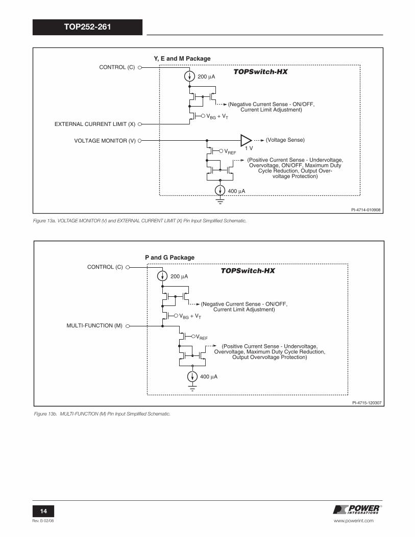
VBG + VT
1 VVREF
200 A
400 A
CONTROL (C)
(Voltage Sense)
(Positive Current Sense - Undervoltage,Overvoltage, ON/OFF, Maximum Duty
Cycle Reduction, Output Over-voltage Protection)
(Negative Current Sense - ON/OFF,Current Limit Adjustment)
PI-4714-010908
TOPSwitch-HX
VOLTAGE MONITOR (V)
EXTERNAL CURRENT LIMIT (X)
Y, E and M Package
VBG + VT
VREF
200 A
400 A
CONTROL (C)
MULTI-FUNCTION (M)
(Positive Current Sense - Undervoltage,Overvoltage, Maximum Duty Cycle Reduction,
Output Overvoltage Protection)
(Negative Current Sense - ON/OFF,Current Limit Adjustment)
PI-4715-120307
TOPSwitch-HX
P and G Package
Figure 13a. VOLTAGE MONITOR (V) and EXTERNAL CURRENT LIMIT (X) Pin Input Simplifi ed Schematic.
Figure 13b. MULTI-FUNCTION (M) Pin Input Simplifi ed Schematic.
Rev. B 02/08
15
TOP252-261
www.powerint.com
Typical Uses of FREQUENCY (F) Pin
PI-2654-071700
DCInput
Voltage
+
-
D
S
CCONTROL
F
PI-2655-071700
DCInput
Voltage
+
-
D
S
CCONTROL
F
Figure 14. Full Frequency Operation (132 kHz). Figure 15. Half Frequency Operation (66 kHz).
Rev. B 02/08
16
TOP252-261
www.powerint.com
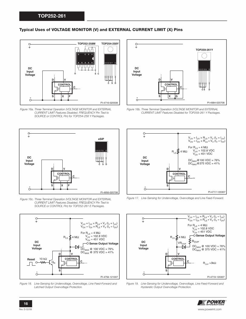
Typical Uses of VOLTAGE MONITOR (V) and EXTERNAL CURRENT LIMIT (X) Pins
X F
PI-4716-020508
DCInput
Voltage
+
-
DC S D
S
CCONTROL
V
V X C S F D
D S C
D C X V
S SS S S
TOP254-258YTOP252-258M
PI-4717-120307
DCInput
Voltage
+
-
D
S
CCONTROL
V
4 MRLS
VUV = IUV × RLS + VV (IV = IUV)VOV = IOV × RLS + VV (IV = IOV)
For RLS = 4 M VUV = 102.8 VDC VOV = 451 VDC
DCMAX@100 VDC = 76%DCMAX@375 VDC = 41%
PI-4756-121007
DCInput
Voltage
Sense Output Voltage
+
-
D V
S
C
VUV = IUV × RLS + VV (IV = IUV)VOV = IOV × RLS + VV (IV = IOV)
For RLS = 4 M VUV = 102.8 VDC VOV = 451 VDC
DCMAX @ 100 VDC = 76%DCMAX @ 375 VDC = 41%
CONTROL
RLS 4 M
10 kResetQR
PI-4719-120307
DCInput
Voltage
Sense Output Voltage
+
-
D V
S
C
VUV = IUV × RLS + VV (IV = IUV)VOV = IOV × RLS + VV (IV = IOV)
For RLS = 4 M VUV = 102.8 VDC VOV = 451 VDC
DCMAX @ 100 VDC = 76% DCMAX @ 375 VDC = 41%
CONTROL
RLS 4 M
ROVP >3k
VROVPROVP
Figure 16a. Three Terminal Operation (VOLTAGE MONITOR and EXTERNAL
CURRENT LIMIT Features Disabled. FREQUENCY Pin Tied to
SOURCE or CONTROL Pin) for TOP254-258 Y Packages.
Figure 17. Line-Sensing for Undervoltage, Overvoltage and Line Feed-Forward.
Figure 18. Line-Sensing for Undervoltage, Overvoltage, Line Feed-Forward and
Latched Output Overvoltage Protection.
Figure 19. Line-Sensing for Undervoltage, Overvoltage, Line Feed-Forward and
Hysteretic Output Overvoltage Protection.
Figure 16c. Three Terminal Operation (VOLTAGE MONITOR and EXTERNAL
CURRENT LIMIT Features Disabled. FREQUENCY Pin Tied to
SOURCE or CONTROL Pin) for TOP252-261 E Packages.
X G
PI-4984-020708
DCInput
Voltage
+
-
D
C S D
S
CCONTROL
V
TOP259-261Y
V X C S G D
Figure 16b. Three Terminal Operation (VOLTAGE MONITOR and EXTERNAL
CURRENT LIMIT Features Disabled for TOP259-261 Y Packages.
X F
DCInput
Voltage
+
-
D
C S D
S
CCONTROL
V
V X C SF D
PI-4956-020708
eSIP

Rev. B 02/08
17
TOP252-261
www.powerint.com
PI-4720-120307
DCInput
Voltage
+
-
D V
S
C
VUV = RLS × IUV + VV (IV = IUV)
For Values Shown VUV = 103.8 VDC
RLS
6.2 V
4 M
40 k
CONTROL
PI-4721-120307
DCInput
Voltage
+
-
D
S
CCONTROL
V
4 M
55 k
RLS
1N4148
VOV = IOV × RLS + VV (IV = IOV)
For Values Shown VOV = 457.2 VDC
Figure 20. Line Sensing for Undervoltage Only (Overvoltage Disabled). Figure 21. Line-Sensing for Overvoltage Only (Undervoltage Disabled). Maximum
Duty Cycle Reduced at Low Line and Further Reduction with
Increasing Line Voltage.
Typical Uses of VOLTAGE MONITOR (V) and EXTERNAL CURRENT LIMIT (X) Pins (cont.)
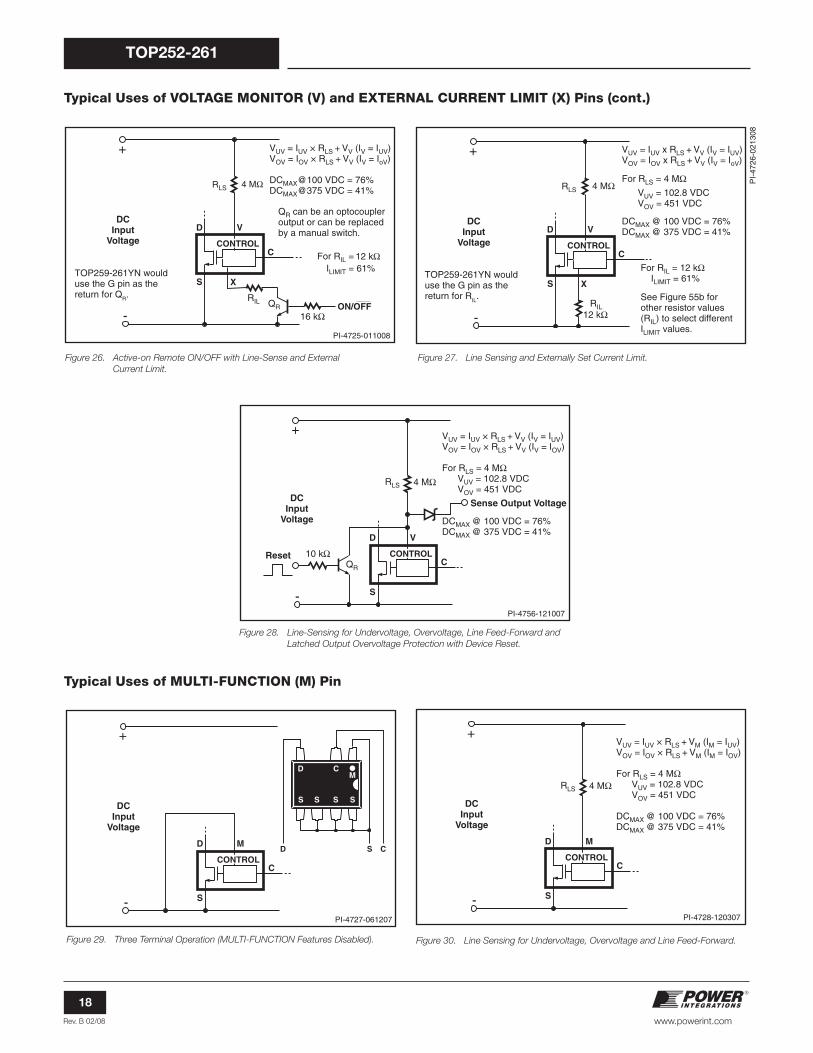
Figure 22. External Set Current Limit.
X
PI-4722-021308
DCInput
Voltage
+
-
D
S
C
RIL
For RIL = 12 k ILIMIT = 61%
See Figure 55b for other resistor values (RIL).
TOP259-261YN would use the G pin as the return for RIL.
For RIL = 19 k ILIMIT = 37%
CONTROL
X
PI-4723-011008
DCInput
Voltage
+
-
D
S
C
2.5 MRLS
6 kRIL
100% @ 100 VDC53% @ 300 VDC
ILIMIT =ILIMIT =
TOP259-261YN would use the G pin as the return for RIL.
CONTROL
X
PI-2625-011008
DCInput
Voltage
+
-
D
S
C
ON/OFF47 K
QR can be an optocoupler output or can be replaced by a manual switch.
TOP259-261YN would use the G pin as the return for QR.
QR
CONTROL
X
ON/OFF16 k
PI-4724-011008
DCInput
Voltage
+
-
D
S
C
RIL QR
12 kFor RIL =
ILIMIT = 61%
19 kFor RIL =
ILIMIT = 37%
QR can be an optocoupler output or can be replaced by a manual switch.
CONTROL
TOP259-261YN would use the G pin as the return for QR.
Figure 23. Current Limit Reduction with Line Voltage.
Figure 24. Active-on (Fail Safe) Remote ON/OFF. Figure 25. Active-on Remote ON/OFF with Externally Set Current Limit.
Rev. B 02/08
18
TOP252-261
www.powerint.com
Typical Uses of VOLTAGE MONITOR (V) and EXTERNAL CURRENT LIMIT (X) Pins (cont.)
PI-4727-061207
DCInput
Voltage
+
-
D
S
CCONTROL
M
D
S SS
D S C
S
CM
PI-4728-120307
DCInput
Voltage
+
-
D M
S
C
VUV = IUV × RLS + VM (IM = IUV)VOV = IOV × RLS + VM (IM = IOV)
For RLS = 4 M VUV = 102.8 VDC VOV = 451 VDC
DCMAX @ 100 VDC = 76%DCMAX @ 375 VDC = 41%
CONTROL
RLS 4 M
Figure 29. Three Terminal Operation (MULTI-FUNCTION Features Disabled). Figure 30. Line Sensing for Undervoltage, Overvoltage and Line Feed-Forward.
Figure 28. Line-Sensing for Undervoltage, Overvoltage, Line Feed-Forward and
Latched Output Overvoltage Protection with Device Reset.
PI-4756-121007
DCInput
Voltage
Sense Output Voltage
+
-
D V
S
C
VUV = IUV × RLS + VV (IV = IUV)VOV = IOV × RLS + VV (IV = IOV)
For RLS = 4 M VUV = 102.8 VDC VOV = 451 VDC
DCMAX @ 100 VDC = 76%DCMAX @ 375 VDC = 41%
CONTROL
RLS 4 M
10 kResetQR
Typical Uses of MULTI-FUNCTION (M) Pin
X
ON/OFF16 k
PI-4725-011008
DCInput
Voltage
+
-
D
S
CCONTROL
V
RIL
RLS
QR
4 M
VUV = IUV × RLS + VV (IV = IUV)VOV = IOV × RLS + VV (IV = IoV)
DCMAX@100 VDC = 76%DCMAX@375 VDC = 41%
12 kFor RIL = ILIMIT = 61%
QR can be an optocoupler output or can be replaced by a manual switch.
TOP259-261YN would use the G pin as the return for QR.
X
PI-
4726
-021
308
DCInput
Voltage
+
-
D
S
CCONTROL
V
RIL
RLS
12 k
4 M
VUV = IUV x RLS + VV (IV = IUV)VOV = IOV x RLS + VV (IV = IoV)
For RLS = 4 M
DCMAX @ 100 VDC = 76%DCMAX @ 375 VDC = 41%
For RIL = 12 k ILIMIT = 61%
See Figure 55b for other resistor values (RIL) to select different ILIMIT values.
VUV = 102.8 VDC VOV = 451 VDC
TOP259-261YN would use the G pin as the return for RIL.
Figure 26. Active-on Remote ON/OFF with Line-Sense and External
Current Limit.
Figure 27. Line Sensing and Externally Set Current Limit.

Rev. B 02/08
19
TOP252-261
www.powerint.com
PI-4729-120307
DCInput
Voltage
Sense Output Voltage
+
-
D M
S
C
VUV = IUV × RLS + VM (IM = IUV)VOV = IOV × RLS + VM (IM = IOV)
For RLS = 4 M VUV = 102.8 VDC VOV = 451 VDC
DCMAX @ 100 VDC = 76%DCMAX @ 375 VDC = 41%
CONTROL
RLS 4 M
Figure 31. Line Sensing for Undervoltage, Overvoltage, Line Feed-Forward and
Latched Output Overvoltage Protection.
PI-4730-120307
DCInput
Voltage
Sense Output Voltage
+
-
D M
S
C
VUV = IUV × RLS + VM (IM = IUV)VOV = IOV × RLS + VM (IM = IOV)
For RLS = 4 M VUV = 102.8 VDC VOV = 451 VDC
DCMAX @ 100 VDC = 76% DCMAX @ 375 VDC = 41%
CONTROL
RLS 4 M
VROVPROVP
ROVP >3k
Figure 32. Line Sensing for Undervoltage, Overvoltage, Line Feed-Forward and
Hysteretic Output Overvoltage Protection.
PI-4731-120307
DCInput
Voltage
+
-
D M
S
C
VUV = RLS × IUV + VM (IM = IUV)
For Values Shown VUV = 103.8 VDC
RLS
6.2 V
4 M
40 k
CONTROL
PI-4732-120307
DCInput
Voltage
+
-
D M
S
C
VOV = IOV × RLS + VM (IM = IOV)
For Values Shown VOV = 457.2 VDC
CONTROL
RLS
1N4148
4 M
55 k
Figure 33. Line Sensing for Undervoltage Only (Overvoltage Disabled). Figure 34. Line Sensing for Overvoltage Only (Undervoltage Disabled). Maximum
Duty Cycle Reduced at Low Line and Further Reduction with
Increasing Line Voltage.
Typical Uses of MULTI-FUNCTION (M) Pin (cont.)
Figure 35. Externally Set Current Limit (Not Normally Required – See M Pin
Operation Description).
PI-4733-021308
DCInput
Voltage
+
-
D M
S
C
For RIL = 12 k ILIMIT = 61%
CONTROLRIL
See Figures 55b for other resistor values (RIL) to select different ILIMIT values.
For RIL = 19 k ILIMIT = 37%
PI-4734-092107
DCInput
Voltage
+
-
D M
S
CCONTROLRIL
RLS 2.5 M
6 k
100% @ 100 VDC53% @ 300 VDC
ILIMIT =ILIMIT =
Figure 36. Current Limit Reduction with Line Voltage (Not Normally Required –
See M Pin Operation Description).

Rev. B 02/08
20
TOP252-261
www.powerint.com
Typical Uses of MULTI-FUNCTION (M) Pin (cont.)
PI-4757-120307
DCInput
Voltage
Sense Output Voltage
+
-
D M
S
C
VUV = IUV × RLS + VM (IM = IUV) VOV = IOV × RLS + VM (IM = IOV)
For RLS = 4 M VUV = 102.8 VDC VOV = 451 VDC
DCMAX @ 100 VDC = 76% DCMAX @ 375 VDC = 41%
CONTROL
RLS 4 M
10 kQR
Reset
Figure 40. Line-Sensing for Undervoltage, Overvoltage, Line Feed-Forward and
Latched Output Overvoltage Protection with Device Reset.
PI-4736-060607
DCInput
Voltage
+
-
D
S
CRIL
RMC 24 k
12 k
M
CONTROL
QR
2RILRMC =
QR can be an optocoupler output or can be replaced by a manual switch.
ON/OFF7 k
Figure 39. Active-off Remote ON/OFF with Externally Set Current Limit
(see M Pin Operation Description).
PI-4735-092107
DCInput
Voltage
+
-
D
S
C
QR
RILM
CONTROL
12 kFor RIL =
ILIMIT = 61%
QR can be an optocoupler output or can be replaced by a manual switch.
ON/OFF16 k
19 kFor RIL =
ILIMIT = 37%
Figure 38. Active-on Remote ON/OFF with Externally Set Current Limit
(see M Pin Operation Description).
PI-2519-040501
DCInput
Voltage
+
-
D
S
CQR
ON/OFF
M
CONTROL
QR can be an optocoupler output or can be replaced by a manual switch.
47 k
Figure 37. Active-on (Fail Safe) Remote ON/OFF.
Rev. B 02/08
21
TOP252-261
www.powerint.com
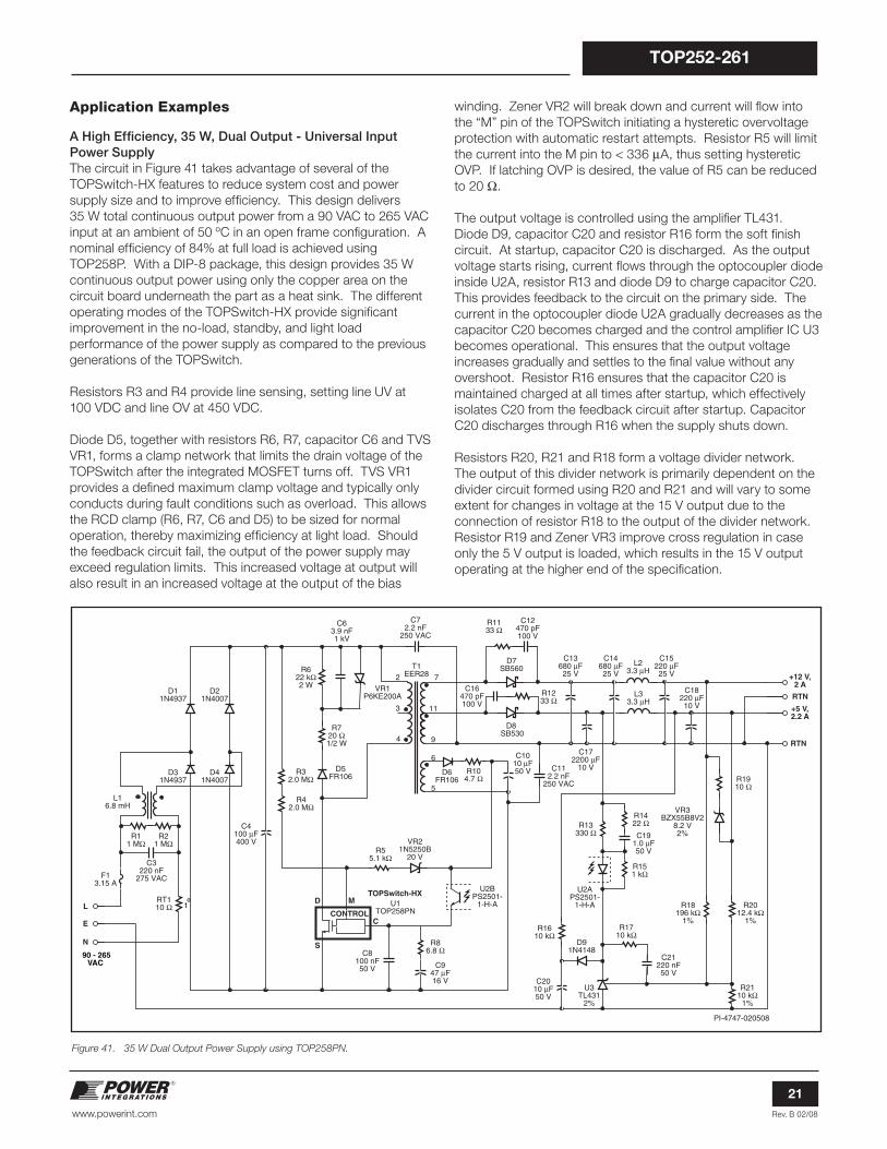
Application Examples
A High Effi ciency, 35 W, Dual Output - Universal InputPower Supply The circuit in Figure 41 takes advantage of several of the
TOPSwitch-HX features to reduce system cost and power
supply size and to improve effi ciency. This design delivers
35 W total continuous output power from a 90 VAC to 265 VAC
input at an ambient of 50 ºC in an open frame confi guration. A
nominal effi ciency of 84% at full load is achieved using
TOP258P. With a DIP-8 package, this design provides 35 W
continuous output power using only the copper area on the
circuit board underneath the part as a heat sink. The different
operating modes of the TOPSwitch-HX provide signifi cant
improvement in the no-load, standby, and light load
performance of the power supply as compared to the previous
generations of the TOPSwitch.
Resistors R3 and R4 provide line sensing, setting line UV at
100 VDC and line OV at 450 VDC.
Diode D5, together with resistors R6, R7, capacitor C6 and TVS
VR1, forms a clamp network that limits the drain voltage of the
TOPSwitch after the integrated MOSFET turns off. TVS VR1
provides a defi ned maximum clamp voltage and typically only
conducts during fault conditions such as overload. This allows
the RCD clamp (R6, R7, C6 and D5) to be sized for normal
operation, thereby maximizing effi ciency at light load. Should
the feedback circuit fail, the output of the power supply may
exceed regulation limits. This increased voltage at output will
also result in an increased voltage at the output of the bias
winding. Zener VR2 will break down and current will fl ow into
the “M” pin of the TOPSwitch initiating a hysteretic overvoltage
protection with automatic restart attempts. Resistor R5 will limit
the current into the M pin to < 336 μA, thus setting hysteretic
OVP. If latching OVP is desired, the value of R5 can be reduced
to 20 Ω.
The output voltage is controlled using the amplifi er TL431.
Diode D9, capacitor C20 and resistor R16 form the soft fi nish
circuit. At startup, capacitor C20 is discharged. As the output
voltage starts rising, current fl ows through the optocoupler diode
inside U2A, resistor R13 and diode D9 to charge capacitor C20.
This provides feedback to the circuit on the primary side. The
current in the optocoupler diode U2A gradually decreases as the
capacitor C20 becomes charged and the control amplifi er IC U3
becomes operational. This ensures that the output voltage
increases gradually and settles to the fi nal value without any
overshoot. Resistor R16 ensures that the capacitor C20 is
maintained charged at all times after startup, which effectively
isolates C20 from the feedback circuit after startup. Capacitor
C20 discharges through R16 when the supply shuts down.
Resistors R20, R21 and R18 form a voltage divider network.
The output of this divider network is primarily dependent on the
divider circuit formed using R20 and R21 and will vary to some
extent for changes in voltage at the 15 V output due to the
connection of resistor R18 to the output of the divider network.
Resistor R19 and Zener VR3 improve cross regulation in case
only the 5 V output is loaded, which results in the 15 V output
operating at the higher end of the specifi cation.
Figure 41. 35 W Dual Output Power Supply using TOP258PN.
D
S
C
M
CONTROL
PI-4747-020508
R1133
R1233
R32.0 M
R1610 k
R1710 k
R2110 k
1%
R18196 k
1%
R1910
R1422R13
330
R151 k
R2012.4 k
1%
D91N4148
U3TL431
2%
VR3BZX55B8V2
8.2 V2%
R7201/2 W
VR21N5250B
20 V
VR1P6KE200A
D5FR106
R42.0 M
R55.1 k
R11 M
R21 M
R86.8
R104.7
R622 k2 W
U2BPS2501-
1-H-A
U2APS2501-
1-H-A
L23.3 H
L16.8 mH
L33.3 H
U1TOP258PN
C947 F16 V C20
10 F50 V
C21220 nF50 V
C191.0 F50 V
C1010 F50 V C11
2.2 nF250 VAC
D6FR106
D8SB530
D7SB560
C8100 nF50 V
D11N4937
D21N4007
D31N4937
D41N4007
C13680 F25 V
C14680 F25 V
C15220 F25 V
C18220 F10 V
C172200 F
10 V
C12470 pF100 V
C16470 pF100 V
2T1
EER28 7
11
9
3
6
5
4
C4100 F400 V
C63.9 nF1 kV
C72.2 nF
250 VAC
C3220 nF
275 VAC
RT110
F13.15 A
TOPSwitch-HX
L
E
N
+12 V,2 A
RTN
+5 V,2.2 A
RTN
tO
90 - 265VAC
Rev. B 02/08
22
TOP252-261
www.powerint.com
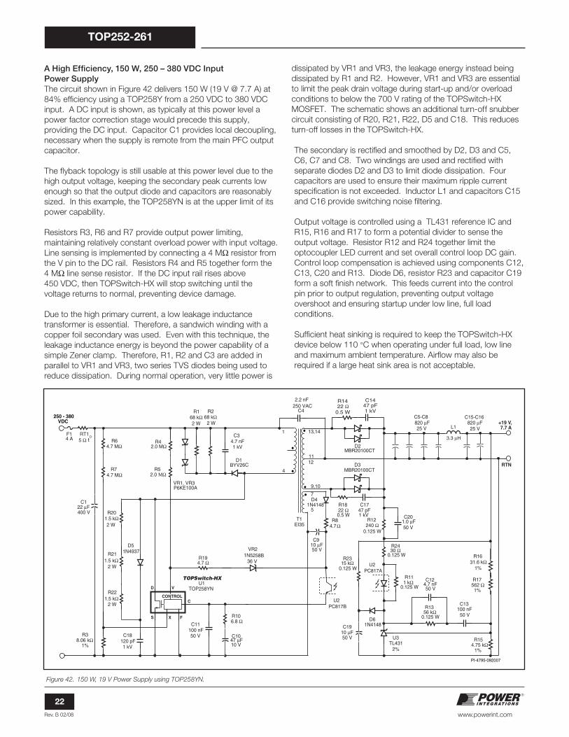
A High Effi ciency, 150 W, 250 – 380 VDC Input Power Supply The circuit shown in Figure 42 delivers 150 W (19 V @ 7.7 A) at
84% effi ciency using a TOP258Y from a 250 VDC to 380 VDC
input. A DC input is shown, as typically at this power level a
power factor correction stage would precede this supply,
providing the DC input. Capacitor C1 provides local decoupling,
necessary when the supply is remote from the main PFC output
capacitor.
The fl yback topology is still usable at this power level due to the
high output voltage, keeping the secondary peak currents low
enough so that the output diode and capacitors are reasonably
sized. In this example, the TOP258YN is at the upper limit of its
power capability.
Resistors R3, R6 and R7 provide output power limiting,
maintaining relatively constant overload power with input voltage.
Line sensing is implemented by connecting a 4 MΩ resistor from
the V pin to the DC rail. Resistors R4 and R5 together form the
4 MΩ line sense resistor. If the DC input rail rises above
450 VDC, then TOPSwitch-HX will stop switching until the
voltage returns to normal, preventing device damage.
Due to the high primary current, a low leakage inductance
transformer is essential. Therefore, a sandwich winding with a
copper foil secondary was used. Even with this technique, the
leakage inductance energy is beyond the power capability of a
simple Zener clamp. Therefore, R1, R2 and C3 are added in
parallel to VR1 and VR3, two series TVS diodes being used to
reduce dissipation. During normal operation, very little power is
dissipated by VR1 and VR3, the leakage energy instead being
dissipated by R1 and R2. However, VR1 and VR3 are essential
to limit the peak drain voltage during start-up and/or overload
conditions to below the 700 V rating of the TOPSwitch-HX
MOSFET. The schematic shows an additional turn-off snubber
circuit consisting of R20, R21, R22, D5 and C18. This reduces
turn-off losses in the TOPSwitch-HX.
The secondary is rectifi ed and smoothed by D2, D3 and C5,
C6, C7 and C8. Two windings are used and rectifi ed with
separate diodes D2 and D3 to limit diode dissipation. Four
capacitors are used to ensure their maximum ripple current
specifi cation is not exceeded. Inductor L1 and capacitors C15
and C16 provide switching noise fi ltering.
Output voltage is controlled using a TL431 reference IC and
R15, R16 and R17 to form a potential divider to sense the
output voltage. Resistor R12 and R24 together limit the
optocoupler LED current and set overall control loop DC gain.
Control loop compensation is achieved using components C12,
C13, C20 and R13. Diode D6, resistor R23 and capacitor C19
form a soft fi nish network. This feeds current into the control
pin prior to output regulation, preventing output voltage
overshoot and ensuring startup under low line, full load
conditions.
Suffi cient heat sinking is required to keep the TOPSwitch-HX
device below 110 °C when operating under full load, low line
and maximum ambient temperature. Airfl ow may also be
required if a large heat sink area is not acceptable.
L1
D41N4148
C11100 nF50 V
+19 V, 7.7 A
RTN
RT15
R194.7
D3MBR20100CTR7
4.7 M
D2MBR20100CT
C15-C16820 F25 V
C1447 pF1 kV
R201.5 k2 W
C1047 F10 V
D1BYV26C
T1EI35
11
4
13,14
5
12
1
9,10
7
R154.75 k
1%
C201.0 F50 V
C1747 pF1 kV
C910 F50 V
R2315 k
0.125 W
R1422
0.5 W
R38.06 k
1%
C4
2.2 nF250 VAC
R106.8
C34.7 nF1 kV
C122 F400 V
R221.5 k
2 W
D61N4148
R84.7
R168 k2 W
F14 A
C18120 pF1 kV
R1631.6 k
1%
R268 k
2 W
VR21N5258B
36 V
R111 k
0.125 W
C1910 F50 V
R12240
0.125 W
U1TOP258YN
R2430
0.125 W
C5-C8
25 V
VR1, VR3P6KE100A
R18220.5 W
R21
2 W
D51N4937
U2PC817A
U3TL431
2%
C124.7 nF50 V
R175621%
R1356 k
0.125 W
C13100 nF
50 V
U2PC817B
3.3 HR4
2.0 M
R52.0
1.5 k
tO
TOPSwitch-HX
R64.7 M
820 F 250 - 380
VDC
PI-4795-092007
D
S
C
V
FX
CONTROL
Figure 42. 150 W, 19 V Power Supply using TOP258YN.
Rev. B 02/08
23
TOP252-261
www.powerint.com
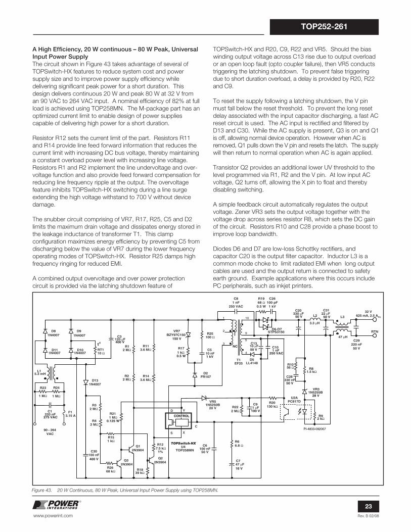
A High Effi ciency, 20 W continuous – 80 W Peak, UniversalInput Power Supply The circuit shown in Figure 43 takes advantage of several of
TOPSwitch-HX features to reduce system cost and power
supply size and to improve power supply effi ciency while
delivering signifi cant peak power for a short duration. This
design delivers continuous 20 W and peak 80 W at 32 V from
an 90 VAC to 264 VAC input. A nominal effi ciency of 82% at full
load is achieved using TOP258MN. The M-package part has an
optimized current limit to enable design of power supplies
capable of delivering high power for a short duration.
Resistor R12 sets the current limit of the part. Resistors R11
and R14 provide line feed forward information that reduces the
current limit with increasing DC bus voltage, thereby maintaining
a constant overload power level with increasing line voltage.
Resistors R1 and R2 implement the line undervoltage and over-
voltage function and also provide feed forward compensation for
reducing line frequency ripple at the output. The overvoltage
feature inhibits TOPSwitch-HX switching during a line surge
extending the high voltage withstand to 700 V without device
damage.
The snubber circuit comprising of VR7, R17, R25, C5 and D2
limits the maximum drain voltage and dissipates energy stored in
the leakage inductance of transformer T1. This clamp
confi guration maximizes energy effi ciency by preventing C5 from
discharging below the value of VR7 during the lower frequency
operating modes of TOPSwitch-HX. Resistor R25 damps high
frequency ringing for reduced EMI.
A combined output overvoltage and over power protection
circuit is provided via the latching shutdown feature of
TOPSwitch-HX and R20, C9, R22 and VR5. Should the bias
winding output voltage across C13 rise due to output overload
or an open loop fault (opto coupler failure), then VR5 conducts
triggering the latching shutdown. To prevent false triggering
due to short duration overload, a delay is provided by R20, R22
and C9.
To reset the supply following a latching shutdown, the V pin
must fall below the reset threshold. To prevent the long reset
delay associated with the input capacitor discharging, a fast AC
reset circuit is used. The AC input is rectifi ed and fi ltered by
D13 and C30. While the AC supply is present, Q3 is on and Q1
is off, allowing normal device operation. However when AC is
removed, Q1 pulls down the V pin and resets the latch. The supply
will then return to normal operation when AC is again applied.
Transistor Q2 provides an additional lower UV threshold to the
level programmed via R1, R2 and the V pin. At low input AC
voltage, Q2 turns off, allowing the X pin to fl oat and thereby
disabling switching.
A simple feedback circuit automatically regulates the output
voltage. Zener VR3 sets the output voltage together with the
voltage drop across series resistor R8, which sets the DC gain
of the circuit. Resistors R10 and C28 provide a phase boost to
improve loop bandwidth.
Diodes D6 and D7 are low-loss Schottky rectifi ers, and
capacitor C20 is the output fi lter capacitor. Inductor L3 is a
common mode choke to limit radiated EMI when long output
cables are used and the output return is connected to safety
earth ground. Example applications where this occurs include
PC peripherals, such as inkjet printers.
C81 nF
250 VAC
D6-D7
C91 F
100 V
R171 k0.5 W
VR7BZY97C150
150 V
T1
D2FR107
D131N4007
F13.15 A
C30100 nF400 V Q3
2N3904
R23
1 M
C1220 nF
275 VAC
90 - 264 VAC
R24
1 M
L15.3 mH
68 k
D101N4007
C3120 F400 V
R113.6 M
D81N4007
RT110
R12 M
R143.6 M
D91N4007
Q22N3904
R1839 k
Q12N3904
R22 M
R32 M
R151 k
R211 M
0.125 WR42 M
R26
C
S
D V
X
R222 M
C6100 nF50 V
U4TOP258MN
C747 F16 V
VR51N5250B
20 V
R25
C510 nF1 kV
R66.8
C101 nF
250 VAC
EF25
R20130 k
D5LL4148
C1310 F50 V
U2APC817D
R92 k
R81.5 k
R1056
VR31N5255B
28 V
C28330 nF50 V
R19680.5 W
STPS3150
C26100 pF1 kV
L3
47 H
L2
3.3 H
C3122 F50 V
C20330 F
50 V
R127.5 k
1%
D111N4007
100
CONTROL
C29220 nF50 V
to
32 V625 mA, 2.5 APK
RTN
PI-4833-092007
1
9
10
5
2
3
4
NC
TOPSwitch-HX
Figure 43. 20 W Continuous, 80 W Peak, Universal Input Power Supply using TOP258MN.
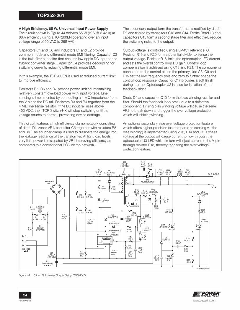
Rev. B 02/08
24
TOP252-261
www.powerint.com
A High Effi ciency, 65 W, Universal Input Power Supply The circuit shown in Figure 44 delivers 65 W (19 V @ 3.42 A) at
88% effi ciency using a TOP260EN operating over an input
voltage range of 90 VAC to 265 VAC.
Capacitors C1 and C6 and inductors L1 and L2 provide
common mode and differential mode EMI fi ltering. Capacitor C2
is the bulk fi lter capacitor that ensures low ripple DC input to the
fl yback converter stage. Capacitor C4 provides decoupling for
switching currents reducing differential mode EMI.
In this example, the TOP260EN is used at reduced current limit
to improve effi ciency.
Resistors R5, R6 and R7 provide power limiting, maintaining
relatively constant overload power with input voltage. Line
sensing is implemented by connecting a 4 MΩ impedance from
the V pin to the DC rail. Resistors R3 and R4 together form the
4 MΩ line sense resistor. If the DC input rail rises above
450 VDC, then TOP Switch-HX will stop switching until the
voltage returns to normal, preventing device damage.
This circuit features a high effi ciency clamp network consisting
of diode D1, zener VR1, capacitor C5 together with resistors R8
and R9. The snubber clamp is used to dissipate the energy into
the leakage reactance of the transformer. At light load levels,
very little power is dissipated by VR1 improving effi ciency as
compared to a conventional RCD clamp network.
The secondary output form the transformer is rectifi ed by diode
D2 and fi ltered by capacitors C13 and C14. Ferrite Bead L3 and
capacitors C15 form a second stage fi lter and effectively reduce
the switching noise to the output.
Output voltage is controlled using a LM431 reference IC.
Resistor R19 and R20 form a potential divider to sense the
output voltage. Resistor R16 limits the optocoupler LED current
and sets the overall control loop DC gain. Control loop
compensation is achieved using C18 and R21. The components
connected to the control pin on the primary side C8, C9 and
R15 set the low frequency pole and zero to further shape the
control loop response. Capacitor C17 provides a soft fi nish
during startup. Optocoupler U2 is used for isolation of the
feedback signal.
Diode D4 and capacitor C10 form the bias winding rectifi er and
fi lter. Should the feedback loop break due to a defective
component, a rising bias winding voltage will cause the zener
VR2 to break down and trigger the over voltage protection
which will inhibit switching.
An optional secondary side over voltage protection feature
which offers higher precision (as compared to sensing via the
bias winding) is implemented using VR2, R14 and U2. Excess
voltage at the output will cause current to fl ow through the
optocoupler U3 LED which in turn will inject current in the V-pin
through resistor R13, thereby triggering the over voltage
protection feature.
Figure 44. 65 W, 19 V Power Supply Using TOP260EN.
PI-4998-021408
R1633
R211 k
R2010 k
R1968.1 k
R1847
R16680
U4LM431
2%
VR3BZX79-C22
22 VD1
DL4937
D61N4148
D3BAV19WS
D5BAV19WS
VR21N5248B
18 V
VR1BZY97C180
180 V
R135.1
R14100
R125.1 k
R112 M
R12.2 M
R22.2 M
R156.8
R1073.2 k
R8100
R91 k
U3BPC357A
U3APC357A
U2BLTY817C
U2ALTY817C
L3FerriteBead
L112 mH
L2Ferrite Bead
U1TOP260EN
C947 F16 V
C161 F50 V
C1733 F35 V
C18100 nF
C11100 nF50 V
C1022 F50 V
D4 BAV19WS
D2MBR20100CT
C8100 nF50 V
C4100 nF400 V
3KBP08MBR1
C13470 F25 V
C14470 F25 V
C1547 F25 V
C121 nF
100 V
4T1
RM10 FL1
FL25
3
2
6
C62.2 nF
250 VAC
C1330 nF
275 VACF14 A TOPSwitch-HX
L
E
N
19 V, 3.42 A
RTN
C2120 F400 V
C3470 pF
250 VAC
C7100 nF25 V
C52.2 nF1 kV
90 - 265VAC
D
S
C
V
FX
CONTROL
R32.0 M
R55.1 M
R42.0 M
R715 k
1%
R66.8 M
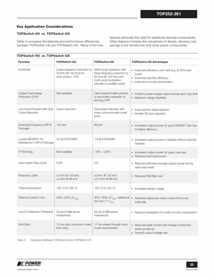
Rev. B 02/08
25
TOP252-261
www.powerint.com
Key Application Considerations
TOPSwitch-HX vs. TOPSwitch-GX
Table 4 compares the features and performance differences
between TOPSwitch-HX and TOPSwitch-GX. Many of the new
features eliminate the need for additional discrete components.
Other features increase the robustness of design, allowing cost
savings in the transformer and other power components.
TOPSwitch-HX vs. TOPSwitch-GX
Function TOPSwitch-GX TOPSwitch-HX TOPSwitch-HX Advantages
EcoSmart Linear frequency reduction to
30 kHz (@ 132 kHz) for
duty cycles < 10%
Multi-mode operation with
linear frequency reduction to
30 kHz (@ 132 kHz) and
multi-cycle modulation
(virtually no audible noise)
Improved effi ciency over load (e.g. at 25% load
point)
Improved standby effi ciency
Improved no-load consumption
•
•
•
Output Overvoltage
Protection (OVP)
Not available User programmable primary
or secondary hysteretic or
latching OVP
Protects power supply output during open loop fault
Maximum design fl exibility
•
•
Line Feed-Forward with Duty
Cycle Reduction
Linear reduction Dual slope reduction with
lower, more accurate onset
point
Improved line ripple rejection
Smaller DC bus capacitor
•
•
Switching Frequency DIP-8
Package
132 kHz 66 kHz Increased output power for given MOSFET size due
to higher effi ciency
•
Lowest MOSFET On
Resistance in DIP-8 Package
3.0 Ω (TOP246P) 1.8 Ω (TOP258P) Increased output power in designs without external
heatsink
•
I2f Trimming Not available -10% / +20% Increased output power for given core size
Reduced over-load power
•
•
Auto-restart Duty Cycle 5.6% 2% Reduced delivered average output power during
open loop faults
•
Frequency Jitter ±4 kHz @ 132 kHz
±2 kHz @ 66 kHz
±5 kHz @ 132 kHz
±2.5 kHz @ 66 kHzReduced EMI fi lter cost•
Thermal Shutdown 130 °C to 150 °C 135 °C to 150 °C Increased design margin•
External Current Limit 30%-100% of ILIMIT
30%-100% of ILIMIT
, additional
trim at 0.7 × ILIMIT
Reduced tolerances when current limit is set
externally
•
Line UV Detection Threshold 50 μA (2 MΩ sense
impedance)
25 μA (4 MΩ sense
impedance)Reduced dissipation for lower no-load consumption•
Soft-Start 10 ms duty cycle and current
limit ramp
17 ms sweep through multi-
mode characteristicReduced peak current and voltage component
stress at startup
Smooth output voltage rise
•
•
Table 4. Comparison Between TOPSwitch-GX and TOPSwitch-HX.

Rev. B 02/08
26
TOP252-261
www.powerint.com
TOPSwitch-HX Design Considerations
Power TableThe data sheet power table (Table 1) represents the maximum
practical continuous output power based on the following
conditions:
12 V output.
Schottky or high effi ciency output diode.
135 V refl ected voltage (VOR
) and effi ciency estimates.
A 100 VDC minimum for 85-265 VAC and 250 VDC mini-
mum for 230 VAC.
Suffi cient heat sinking to keep device temperature ≤100 °C.
Power levels shown in the power table for the M/P package
device assume 6.45 cm2 of 610 g/m2 copper heat sink area
in an enclosed adapter, or 19.4 cm2 in an open frame.
The provided peak power depends on the current limit for the
respective device.
TOPSwitch-HX SelectionSelecting the optimum TOPSwitch-HX depends upon required
maximum output power, effi ciency, heat sinking constraints,
system requirements and cost goals. With the option to
externally reduce current limit, an Y, E or M package
TOPSwitch-HX may be used for lower power applications
where higher effi ciency is needed or minimal heat sinking is
available.
Input CapacitorThe input capacitor must be chosen to provide the minimum
DC voltage required for the TOPSwitch-HX converter to
maintain regulation at the lowest specifi ed input voltage and
maximum output power. Since TOPSwitch-HX has a high
DCMAX
limit and an optimized dual slope line feed forward for
ripple rejection, it is possible to use a smaller input capacitor.
For TOPSwitch-HX, a capacitance of 2 μF per watt is possible
for universal input with an appropriately designed transformer.
Primary Clamp and Output Refl ected Voltage VOR
A primary clamp is necessary to limit the peak TOPSwitch-HX
drain to source voltage. A Zener clamp requires few parts and
takes up little board space. For good effi ciency, the clamp
Zener should be selected to be at least 1.5 times the output
refl ected voltage VOR
, as this keeps the leakage spike
conduction time short. When using a Zener clamp in a
universal input application, a VOR
of less than 135 V is
recommended to allow for the absolute tolerances and
temperature variations of the Zener. This will ensure effi cient
operation of the clamp circuit and will also keep the maximum
drain voltage below the rated breakdown voltage of the
TOPSwitch-HX MOSFET. A high VOR
is required to take full
advantage of the wider DCMAX
of TOPSwitch-HX. An RCD
clamp provides tighter clamp voltage tolerance than a Zener
clamp and allows a VOR as high as 150 V. RCD clamp
dissipation can be minimized by reducing the external current
limit as a function of input line voltage (see Figures 23 and 36).
The RCD clamp is more cost effective than the Zener clamp but
requires more careful design (see Quick Design Checklist).
Output DiodeThe output diode is selected for peak inverse voltage, output
current, and thermal conditions in the application (including
1.
2.
3.
4.
5.
6.
heat sinking, air circulation, etc.). The higher DCMAX
of
TOPSwitch-HX, along with an appropriate transformer turns
ratio, can allow the use of a 80 V Schottky diode for higher
effi ciency on output voltages as high as 15 V (see Figure 41).
Bias Winding CapacitorDue to the low frequency operation at no-load, a 10 μF bias
winding capacitor is recommended.
Soft-StartGenerally, a power supply experiences maximum stress at
start-up before the feedback loop achieves regulation. For a
period of 17 ms, the on-chip soft-start linearly increases the
drain peak current and switching frequency from their low
starting values to their respective maximum values. This
causes the output voltage to rise in an orderly manner, allowing
time for the feedback loop to take control of the duty cycle.
This reduces the stress on the TOPSwitch-HX MOSFET, clamp
circuit and output diode(s), and helps prevent transformer
saturation during start-up. Also, soft-start limits the amount of
output voltage overshoot and, in many applications, eliminates
the need for a soft-fi nish capacitor.
EMIThe frequency jitter feature modulates the switching frequency
over a narrow band as a means to reduce conducted EMI peaks
associated with the harmonics of the fundamental switching
frequency. This is particularly benefi cial for average detection
mode. As can be seen in Figure 45, the benefi ts of jitter increase
with the order of the switching harmonic due to an increase in
frequency deviation. Devices in the P, G or M package and
TOP259-261YN operate at a nominal switching frequency of
66 kHz. The FREQUENCY pin of devices in the TOP254-258 Y
and E packages offer a switching frequency option of 132 kHz or
66 kHz. In applications that require heavy snubber on the drain
node for reducing high frequency radiated noise (for example,
video noise sensitive applications such as VCRs, DVDs, monitors,
TVs, etc.), operating at 66 kHz will reduce snubber loss, resulting
in better effi ciency. Also, in applications where transformer size is
not a concern, use of the 66 kHz option will provide lower EMI
and higher effi ciency. Note that the second harmonic of 66 kHz
is still below 150 kHz, above which the conducted EMI
specifi cations get much tighter. For 10 W or below, it is possible
to use a simple inductor in place of a more costly AC input
common mode choke to meet worldwide conducted EMI limits.
Transformer DesignIt is recommended that the transformer be designed for
maximum operating fl ux density of 3000 Gauss and a peak fl ux
density of 4200 Gauss at maximum current limit. The turns
ratio should be chosen for a refl ected voltage (VOR
) no greater
than 135 V when using a Zener clamp or 150 V (max) when
using an RCD clamp with current limit reduction with line
voltage (overload protection). For designs where operating
current is signifi cantly lower than the default current limit, it is
recommended to use an externally set current limit close to the
operating peak current to reduce peak fl ux density and peak
power (see Figures 22 and 35). In most applications, the tighter
current limit tolerance, higher switching frequency and soft-start
features of TOPSwitch-HX contribute to a smaller transformer
when compared to TOPSwitch-GX.
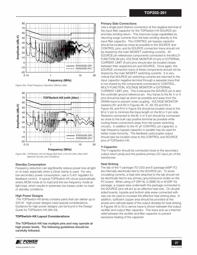
Rev. B 02/08
27
TOP252-261
www.powerint.com
Figure 45b. TOPSwitch-HX Full Range EMI Scan (132 kHz With Jitter) With
Identical Circuitry and Conditions.
-20
-10
0
-10
20
30
40
50
60
70
80
0.15 1 10 30
Frequency (MHz)
Am
plit
ud
e (d
BV
)
PI-
2576
-010
600
EN55022B (QP)EN55022B (AV)
EN55022B (QP)EN55022B (AV)
-20
-10
0
-10
20
30
40
50
60
70
80
0.15 1 10 30
Frequency (MHz)
Am
plit
ud
e (d
BV
)
PI-
2577
-010
600
TOPSwitch-HX (with jitter)
Figure 45a. Fixed Frequency Operation Without Jitter.
Standby ConsumptionFrequency reduction can signifi cantly reduce power loss at light
or no load, especially when a Zener clamp is used. For very
low secondary power consumption, use a TL431 regulator for
feedback control. A typical TOPSwitch-HX circuit automatically
enters MCM mode at no load and the low frequency mode at
light load, which results in extremely low losses under no-load
or standby conditions.
High Power Designs The TOPSwitch-HX family contains parts that can deliver up to
333 W. High power designs need special considerations.
Guidance for high power designs can be found in the Design
Guide for TOPSwitch-HX (AN-43).
TOPSwitch-HX Layout Considerations
The TOPSwitch-HX has multiple pins and may operate at high power levels. The following guidelines should be carefully followed.
Primary Side ConnectionsUse a single point (Kelvin) connection at the negative terminal of
the input fi lter capacitor for the TOPSwitch-HX SOURCE pin
and bias winding return. This improves surge capabilities by
returning surge currents from the bias winding directly to the
input fi lter capacitor. The CONTROL pin bypass capacitor
should be located as close as possible to the SOURCE and
CONTROL pins, and its SOURCE connection trace should not
be shared by the main MOSFET switching currents. All
SOURCE pin referenced components connected to the MULTI-
FUNCTION (M-pin), VOLTAGE MONITOR (V-pin) or EXTERNAL
CURRENT LIMIT (X-pin) pins should also be located closely
between their respective pin and SOURCE. Once again, the
SOURCE connection trace of these components should not be
shared by the main MOSFET switching currents. It is very
critical that SOURCE pin switching currents are returned to the
input capacitor negative terminal through a separate trace that
is not shared by the components connected to CONTROL,
MULTI-FUNCTION, VOLTAGE MONITOR or EXTERNAL
CURRENT LIMIT pins. This is because the SOURCE pin is also
the controller ground reference pin. Any traces to the M, V or X
pins should be kept as short as possible and away from the
DRAIN trace to prevent noise coupling. VOLTAGE MONITOR
resistors (R1 and R2 in Figures 46, 47, 48, R3 and R4 in
Figure 49, and R14 in Figure 50) should be located close to the
M or V pin to minimize the trace length on the M or V pin side.
Resistors connected to the M, V or X pin should be connected
as close to the bulk cap positive terminal as possible while
routing these connections away from the power switching
circuitry. In addition to the 47 μF CONTROL pin capacitor, a
high frequency bypass capacitor in parallel may be used for
better noise immunity. The feedback optocoupler output
should also be located close to the CONTROL and SOURCE
pins of TOPSwitch-HX.
Y-CapacitorThe Y-capacitor should be connected close to the secondary
output return pin(s) and the positive primary DC input pin of the
transformer.
Heat SinkingThe tab of the Y package (TO-220) and E package (eSIP-7C)
are internally electrically tied to the SOURCE pin. To avoid
circulating currents, a heat sink attached to the tab should not
be electrically tied to any primary ground/source nodes on the
PC board. When using a P (DIP-8), G (SMD-8) or M (DIP-10)
package, a copper area underneath the package connected to
the SOURCE pins will act as an effective heat sink. On double
sided boards, topside and bottom side areas connected with
vias can be used to increase the effective heat sinking area. In
addition, suffi cient copper area should be provided at the
anode and cathode leads of the output diode(s) for heat sinking.
In Figures 46 to 50 a narrow trace is shown between the output
rectifi er and output fi lter capacitor. This trace acts as a thermal
relief between the rectifi er and fi lter capacitor to prevent
excessive heating of the capacitor.
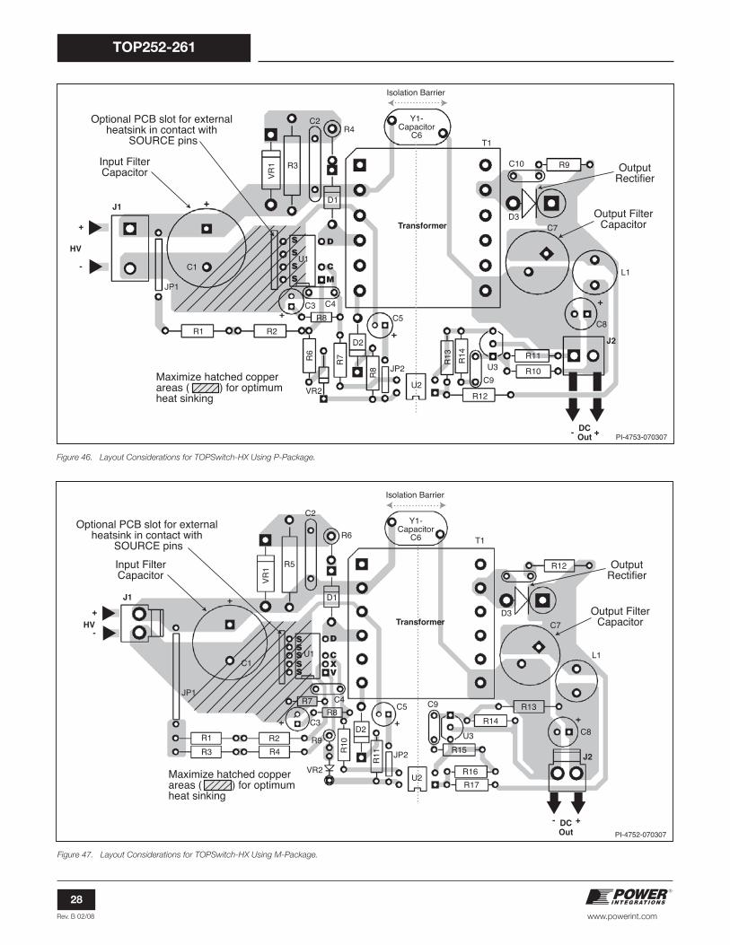
Rev. B 02/08
28
TOP252-261
www.powerint.com
Figure 46. Layout Considerations for TOPSwitch-HX Using P-Package.
Figure 47. Layout Considerations for TOPSwitch-HX Using M-Package.
+- DCOut
+
-
HV
PI-4753-070307
Y1-Capacitor
C6
Isolation Barrier
OutputRectifier
R1 R2
JP1
J1
C1U1
R3
C2R4
D1
VR
1
C4C3
R8
D2
VR2
C5
C9
D3C7
L1
C8
J2
R8
R13
R14R6
R7
JP2
R12
R11
R10U3
R9C10
T1
Output FilterCapacitor
Input FilterCapacitor
Maximize hatched copper areas ( ) for optimum heat sinking
U2
Transformer
DSS
SS
CM
Optional PCB slot for external heatsink in contact with
SOURCE pins
+- DCOut
+
-HV
PI-4752-070307
Isolation Barrier
OutputRectifier
R1
JP1
J1
C1U1
R5
C2
R6
D1
VR
1
C4R7
C3R8
R9D2
C5
D3
C7
L1
C8
J2R11R
10
JP2
C9
R15
U3
R16
R17
R14
R12
T1
R13
VR2
R2
R3 R4
Output FilterCapacitor
Input FilterCapacitor
Optional PCB slot for external heatsink in contact with
SOURCE pins
Maximize hatched copper areas ( ) for optimum heat sinking
SS D
CXV
SSS
U2
Y1-Capacitor
C6
Transformer

Rev. B 02/08
29
TOP252-261
www.powerint.com
Figure 48. Layout Considerations for TOPSwitch-HX Using TOP254-258 Y-Package.
+- DCOut
+
-HV
PI-4751-070307
Y1-Capacitor
C6
Isolation Barrier
OutputRectifier
R1 R2
R3 R4
JP1
J1
C1
U1HS1
R3
C2
R4
D1
VR
1
C4
R7 R10R13
D2
VR2
C5 C9
D3
C7
L1
C8
J2
R9
R11
R16 R
14
R8
JP2
R12R17
R15
U3
R12
C10
T1
Output FilterCapacitor
Input FilterCapacitor
Transformer
S F
C
X V
D
U2
Figure 49. Layout Considerations for TOPSwitch-HX Using TOP259-261 Y-Package.
+
-HV
+- DCOut
PI-4977-021408
Y1-Capacitor
C7
Isolation Barrier
J1
J2
C4 HS1
R3
R22
R14 R8
C9
C8
U5
D5
R7C6
R6VR1
R9
R5
VR2
R10
D6 C10
JP2
R11
R4L3C17
D8
R12C16
R15
U4 C21
R17
R13
R21
R20
C18
JP1
U2
T1
Output FilterCapacitor
Input FilterCapacitor
Transformer
CG
D
V
S
X

Rev. B 02/08
30
TOP252-261
www.powerint.com
+- DCOut
+
-HV
PI-4975-022108
Y1-Capacitor
C7
Isolation Barrier
OutputRectifier
R4
R3
R11
R5
U1
C9
R22R8
R14D6
C10
R10
JP2U2
U4
HS1
R17
C21
R13
R15 R21
R9
VR2
R6 D5
R7
VR1
C6
C4
C8
H52
C17
C18
R20
L3
C19
D8
C16 R12T1
Output FilterCapacitor
Input FilterCapacitor
Transformer
J1
J2
XF
D
C
S
V
Figure 50a. Layout Considerations for TOPSwitch-HX Using E-Package and Operating at 66 KHz.
+
-HV
+- DCOut PI-4976-022108
Y1-Capacitor
C7
Isolation Barrier
OutputRectifier
R4
R3
R11
R5
J1
J2
U1
R6D5
C6 R7
R8
C8
R22
D6C10
R10
R9VR2
C9
R14
VR1
H51C4
U2
R15R13
R17
JP2
U4
C21
R21
R20C19
L3
H52D8
C16 R12
C18
C17
Output FilterCapacitor
Input FilterCapacitor
Transformer
XF
D
C
S
V
Figure 50b. Layout Considerations for TOPSwitch-HX Using E-Package and Operating at 132 KHz.

Rev. B 02/08
31
TOP252-261
www.powerint.com
Quick Design Checklist
In order to reduce the no-load input power of TOPSwitch-HX
designs, the V-pin (or M-pin for P Package) operates at very
low current. This requires careful layout considerations when
designing the PCB to avoid noise coupling. Traces and
components connected to the V-pin should not be adjacent to
any traces carrying switching currents. These include the drain,
clamp network, bias winding return or power traces from other
converters. If the line sensing features are used, then the sense
resistors must be placed within 10 mm of the V-pin to minimize
the V pin node area. The DC bus should then be routed to the
line sense resistors. Note that external capacitance must not
be connected to the V-pin as this may cause misoperaton of the
V pin related functions.
As with any power supply design, all TOPSwitch-HX designs
should be verifi ed on the bench to make sure that components
specifi cations are not exceeded under worst-case conditions.
The following minimum set of tests is strongly recommended:
Maximum drain voltage – Verify that peak VDS
does not
exceed 675 V at highest input voltage and maximum
overload output power. Maximum overload output power
occurs when the output is overloaded to a level just before
the power supply goes into auto-restart (loss of regulation).
1.
Maximum drain current – At maximum ambient temperature,
maximum input voltage and maximum output load, verify
drain current waveforms at start-up for any signs of trans-
former saturation and excessive leading edge current spikes.
TOPSwitch-HX has a leading edge blanking time of 220 ns
to prevent premature termination of the ON-cycle. Verify that
the leading edge current spike is below the allowed current
limit envelope (see Figure 53) for the drain current waveform
at the end of the 220 ns blanking period.
Thermal check – At maximum output power, both minimum
and maximum voltage and ambient temperature; verify that
temperature specifi cations are not exceeded for
TOPSwitch-HX, transformer, output diodes and output
capacitors. Enough thermal margin should be allowed for
the part-to-part variation of the RDS(ON)
of TOPSwitch-HX, as
specifi ed in the data sheet. The margin required can either
be calculated from the values in the parameter table or it can
be accounted for by connecting an external resistance in
series with the DRAIN pin and attached to the same heat
sink, having a resistance value that is equal to the difference
between the measured RDS(ON)
of the device under test and
the worst case maximum specifi cation.
Design Tools
Up-to-date information on design tools can be found at the
Power Integrations website: www.powerint.com
2.
3.

Rev. B 02/08
32
TOP252-261
www.powerint.com
Absolute Maximum Ratings(2)
DRAIN Peak Voltage .................................................................. -0.3 V to 700 V
DRAIN Peak Current: TOP252 ................................................................ 0.68 A
DRAIN Peak Current: TOP253 ................................................................. 1.37 A
DRAIN Peak Current: TOP254 ................................................................ 2.08 A
DRAIN Peak Current: TOP255 .................................................................2.72 A
DRAIN Peak Current: TOP256 ................................................................ 4.08 A
DRAIN Peak Current: TOP257 ................................................................ 5.44 A
DRAIN Peak Current: TOP258 ................................................................ 6.88 A
DRAIN Peak Current: TOP259 ................................................................. 7.73 A
DRAIN Peak Current: TOP260 ................................................................ 9.00 A
DRAIN Peak Current: TOP261 ............................................................... 11.10 A
CONTROL Voltage ............................................................................-0.3 V to 9 V
CONTROL Current ...................................................................................... 100 mA
VOLTAGE MONITOR Pin Voltage .............................................-0.3 V to 9 V
CURRENT LIMIT Pin Voltage ................................................-0.3 V to 4.5 V
MULTI-FUNCTION Pin Voltage .................................................-0.3 V to 9 V
FREQUENCY Pin Voltage ........................................................... -0.3 V to 9 V
Storage Temperature ...........................................................-65 °C to 150 °C
Operating Junction Temperature ................................... -40 °C to 150 °C
Lead Temperature(1) ......................................................................................260 °C
Notes:
1. 1/16 in. from case for 5 seconds.
2. Maximum ratings specifi ed may be applied one at a time
without causing permanent damage to the product. Exposure
to Absolute Maximum Rating conditions for extended periods
of time may affect product reliability.
Thermal Impedance
Thermal Impedance: Y Package:
(θJA
) .................................................................. 80 °C/W(1)
(θJC
) ............................................... .....................2 °C/W(2)
P, G and M Packages: (θ
JA) .........................................70 °C/W(3); 60 °C/W(4)
(θJC
) ............................................... ..................11 °C/W(5)
E Package:
(θJA
) ................................................................105 °C/W(1)
(θJC
) ............................................... .....................2 °C/W(2)
Notes:
1. Free standing with no heatsink.
2. Measured at the back surface of tab.
3. Soldered to 0.36 sq. in. (232 mm2), 2 oz. (610 g/m2) copper clad.
4. Soldered to 1 sq. in. (645 mm2), 2 oz. (610 g/m2) copper clad.
5. Measured on the SOURCE pin close to plastic interface.
Parameter Symbol
Conditions
SOURCE = 0 V; TJ = -40 to 125 °C
See Figure 54
(Unless Otherwise Specifi ed)
Min Typ Max Units
Control Functions
Switching Frequency
in Full Frequency
Mode (average)
fOSC
TJ = 25 °C
FREQUENCY PinConnected to SOURCE
119 132 145
kHz
E Package and TOP254-TOP258 in Y Package
FREQUENCY PinConnected to CONTROL 59.5 66 72.5
M/P/G/Y/E Packages
Frequency Jitter Δf132 kHz Operation ±5
kHz66 kHz Operation ±2.5
Frequency Jitter
Modulation RatefM
250 Hz
Maximum Duty Cycle DCMAX
IC = I
CD1
IV ≤ I
V(DC) or I
M ≤ I
M(DC) or
VV, V
M = 0 V
75 78 83%
IV or I
M = 95 μA 30
Soft-Start Time tSOFT
TJ = 25 °C 17 ms
PWM Gain DCreg
TJ = 25 °C
TOP252-255 -31 -25 -20
%/mATOP256-258 -27 -22 -17
TOP259-261 -25 -20 -15
PWM Gain
Temperature DriftSee Note A -0.01 %/mA/°C
External Bias Current IB
66 kHz Operation
TOP252-255 0.9 1.5 2.1
mA
TOP256-258 1.0 1.6 2.2
TOP259-261 1.1 1.7 2.3
132 kHz OperationTOP252-255 1.0 1.6 2.2
TOP256-258 1.3 1.9 2.5
TOP259-261 1.6 2.2 2.8

Rev. B 02/08
33
TOP252-261
www.powerint.com
Parameter Symbol
Conditions
SOURCE = 0 V; TJ = -40 to 125 °C
(Unless Otherwise Specifi ed)
Min Typ Max Units
Control Functions (cont.)
CONTROL Current at
0% Duty CycleIC(OFF)
66 kHz Operation
TOP252-255 4.4 5.8
mA
TOP256-258 4.7 6.1
TOP259-261 5.1 6.5
132 kHz Operation
TOP254-255 4.6 6.0
TOP256-258 5.1 6.5
TOP259-261 5.9 7.3
Dynamic
ImpedanceZ
CIC = 4 mA; T
J = 25 °C, See Figure 52 10 18 22 Ω
Dynamic Impedance
Temperature Drift0.18 %/°C
CONTROL Pin Internal
Filter Pole7 kHz
Upper Peak Current to
Set Current Limit Ratiok
PS(UPPER)T
J = 25 °C 50 55 60 %
Lower Peak Current to
Set Current Limit Ratiok
PS(LOWER)T
J = 25 °C 25 %
Multi-Cycle-
Modulation Switching
Frequency
fMCM(MIN)
TJ = 25 °C 30 kHz
Minimum Multi-Cycle-
Modulation On PeriodT
MCM(MIN)T
J = 25 °C 135 μs
Shutdown/Auto-Restart
Control Pin
Charging CurrentIC(CH)
TJ = 25 °C
VC = 0 V -5.0 -3.5 -1.0
mAV
C = 5 V -3.0 -1.8 -0.6
Charging Current
Temperature DriftSee Note A 0.5 %/°C
Auto-Restart
Upper Threshold
Voltage
VC(AR)U
5.8 V
Auto-Restart Lower
Threshold VoltageV
C(AR)L4.5 4.8 5.1 V
Multi-Function (M), Voltage Monitor (V) and External Current Limit (X) Inputs
Auto-Restart
Hysteresis VoltageV
C(AR)hyst0.8 1.0 V
Auto-Restart Duty
CycleDC
(AR)2 4 %
Auto-Restart
Frequencyf(AR)
0.5 Hz
Line Undervoltage
Threshold Current and
Hysteresis (M or V Pin)
IUV
TJ = 25 °C
Threshold 22 25 27 μA
Hysteresis 14 μA
Line Overvoltage
Threshold Current and
Hysteresis (M or V Pin)
IOV
TJ = 25 °C
Threshold 107 112 117 μA
Hysteresis 4 μA

Rev. B 02/08
34
TOP252-261
www.powerint.com
Parameter Symbol
ConditionsSOURCE = 0 V; T
J = -40 to 125 °C
(Unless Otherwise Specifi ed)
Min Typ Max Units
Multi-Function (M), Voltage Monitor (V) and External Current Limit (X) Inputs
Output Overvoltage
Latching Shutdown
Threshold Current
IOV(LS)
TJ = 25 °C 269 336 403 μA
V or M Pin Reset Voltage V
V(TH) or
VM(TH)
TJ = 25 °C 0.8 1.0 1.6 V
Remote ON/OFF
Negative Threshold
Current and Hysteresis
(M or X Pin)
IREM (N)
TJ = 25 °C
Threshold -35 -27 -20
μA
Hysteresis 5
V or M Pin Short Circuit
Current
IV(SC)
or
IM(SC)
TJ = 25 °C V
V, V
M = V
C300 400 500 μA
X or M Pin Short Circuit
Current
IX(SC)
or
IM(SC)
VX, V
M = 0 V
Normal Mode -260 -200 -140μA
Auto-Restart Mode -95 -75 -55
V or M Pin Voltage
(Positive Current)V
V or
V
M
IV or I
M = I
UV2.10 2.8 3.20
VIV or I
M = I
OV
TOP252-TOP257 2.79 3.0 3.21
TOP258-TOP261 2.83 3.0 3.25
V or M Pin Voltage
Hysteresis (Positive
Current)
VV(hyst)
or
VM(hyst)
IV or I
M = I
OV0.2 0.5 V
X or M Pin Voltage
(Negative Current)V
X or V
M
IX or I
M = -50 μA 1.23 1.30 1.37
VIX or I
M = -150 μA 1.15 1.22 1.29
Maximum Duty Cycle
Reduction Onset
Threshold Current
IV(DC)
or
IM(DC)
IC ≥ I
B, T
J = 25 °C 18.9 22.0 24.2 μA
Maximum Duty Cycle
Reduction SlopeT
J = 25 °C
IV(DC)
< IV <48 μA or
IM(DC)
< IM
<48 μA-1.0
%/μA
IV or I
M ≥48 μA -0.25
Remote OFF DRAIN
Supply CurrentID(RMT)
VDRAIN
= 150 V
X, V or M Pin
Floating0.6 1.0
mAV or M Pin Shorted to
CONTROL1.0 1.6
Remote ON Delay tR(ON)
From Remote ON to Drain
Turn-On
See Note B
66 kHz 3.0
μs132 kHz 1.5
Remote OFF Setup Time tR(OFF)
Minimum Time Before Drain
Turn-On to Disable Cycle
See Note B
66 kHz 3.0
μs132 kHz 1.5
Frequency Input
FREQUENCY Pin
Threshold VoltageV
FSee Note B 2.9 V
FREQUENCY Pin Input
CurrentIF
TJ = 25 °C V
F = V
C10 55 90 μA

Rev. B 02/08
35
TOP252-261
www.powerint.com
Parameter Symbol
ConditionsSOURCE = 0 V; T
J = -40 to 125 °C
(Unless Otherwise Specifi ed)
Min Typ Max Units
Circuit Protection
Self Protection
Current Limit
(See Note C)
ILIMIT
TOP252PN/GN/MN
TJ = 25 °C
di/dt = 45 mA/μs 0.400 0.43 0.460
A
TOP252EN
TJ = 25 °C
di/dt = 90 mA/μs 0.400 0.43 0.460
TOP253PN/GN
TJ = 25 °C
di/dt = 80 mA/μs 0.697 0.75 0.803
TOP253MN
TJ = 25 °C
di/dt = 90 mA/μs 0.790 0.85 0.910
TOP253EN
TJ = 25 °C
di/dt = 180 mA/μs 0.790 0.85 0.910
TOP254PN/GN
TJ = 25 °C
di/dt = 105 mA/μs 0.93 1.00 1.07
TOP254MN
TJ = 25 °C
di/dt = 135 mA/μs 1.209 1.30 1.391
TOP254YN/EN
TJ = 25 °C
di/dt = 270 mA/μs 1.209 1.30 1.391
TOP255PN/GN
TJ = 25 °C
di/dt = 120 mA/μs 1.069 1.15 1.231
TOP255MN
TJ = 25 °C
di/dt = 175 mA/μs 1.581 1.70 1.819
TOP255YN/EN
TJ = 25 °C
di/dt = 350 mA/μs 1.581 1.70 1.819
TOP256PN/GN
TJ = 25 °C
di/dt = 140 mA/μs 1.255 1.35 1.445
TOP256MN
TJ = 25 °C
di/dt = 220 mA/μs 1.953 2.10 2.247
TOP256YN/EN
TJ = 25 °C
di/dt = 530 mA/μs 2.371 2.55 2.729
TOP257PN/GN
TJ = 25 °C
di/dt = 155 mA/μs 1.395 1.50 1.605
TOP257MN
TJ = 25 °C
di/dt = 265 mA/μs 2.371 2.55 2.729
TOP257YN/EN
TJ = 25 °C
di/dt = 705 mA/μs 3.162 3.40 3.638
TOP258PN/GN
TJ = 25 °C
di/dt = 170 mA/μs 1.534 1.65 1.766
TOP258MN
TJ = 25 °C
di/dt = 310 mA/μs 2.790 3.00 3.210
TOP258YN/EN
TJ = 25 °C
di/dt = 890 mA/μs 3.999 4.30 4.601
TOP259YN/EN
TJ = 25 °C
di/dt = 1065 mA/μs 4.790 5.15 5.511
TOP260YN/EN
TJ = 25 °C
di/dt = 1240 mA/μs 5.580 6.00 6.420
TOP261YN/EN
TJ = 25 °C
di/dt = 1530 mA/μs 6.882 7.40 7.918

Rev. B 02/08
36
TOP252-261
www.powerint.com
Parameter Symbol
ConditionsSOURCE = 0 V; T
J = -40 to 125 °C
(Unless Otherwise Specifi ed)
Min Typ Max Units
Circuit Protection (cont.)
Initial Current Limit IINIT
See Note B0.70 ×
ILIMIT(MIN)
A
Power Coeffi cient PCOEFF
TJ = 25 °C,
See Note D
IX or I
M ≤ - 165 μA 0.9 × I2 I2f 1.2 × I2f
A2kHzIX or I
M ≤ - 117 μA 0.9 × I2 I2f 1.2 × I2f
Leading Edge
Blanking TimetLEB
TJ = 25 °C, See Figure 53 220 ns
Current Limit Delay tIL(D)
100 ns
Thermal Shutdown
Temperature135 142 150 °C
Thermal Shutdown
Hysteresis75 °C
Power-Up Reset
Threshold VoltageV
C(RESET)Figure 54 (S1 Open Condition) 1.75 3.0 4.25 V
Output
ON-State
ResistanceR
DS(ON)
TOP252
ID = 50 mA
TJ = 25 °C 19.1 22.00
Ω
TJ = 100 °C 28.8 33.40
TOP253
ID = 100 mA
TJ = 25 °C 8.8 10.10
TJ = 100 °C 13.1 15.20
TOP254
ID = 150 mA
TJ = 25 °C 5.4 6.25
TJ = 100 °C 8.35 9.70
TOP255
ID = 200 mA
TJ = 25 °C 4.1 4.70
TJ = 100 °C 6.3 7.30
TOP256
ID = 300 mA
TJ = 25 °C 2.8 3.20
TJ = 100 °C 4.1 4.75
TOP257
ID = 400 mA
TJ = 25 °C 2.0 2.30
TJ = 100 °C 3.1 3.60
TOP258
ID = 500 mA
TJ = 25 °C 1.7 1.95
TJ = 100 °C 2.5 2.90
TOP259
ID = 600 mA
TJ = 25 °C 1.45 1.70
TJ = 100 °C 2.25 2.60
TOP260
ID = 700 mA
TJ = 25 °C 1.20 1.40
TJ = 100 °C 1.80 2.10
TOP261
ID = 800 mA
TJ = 25 °C 1.05 1.20
TJ = 100 °C 1.55 1.80
DRAIN Supply Voltage TJ ≤ 85 °C, See Note E
18V
36
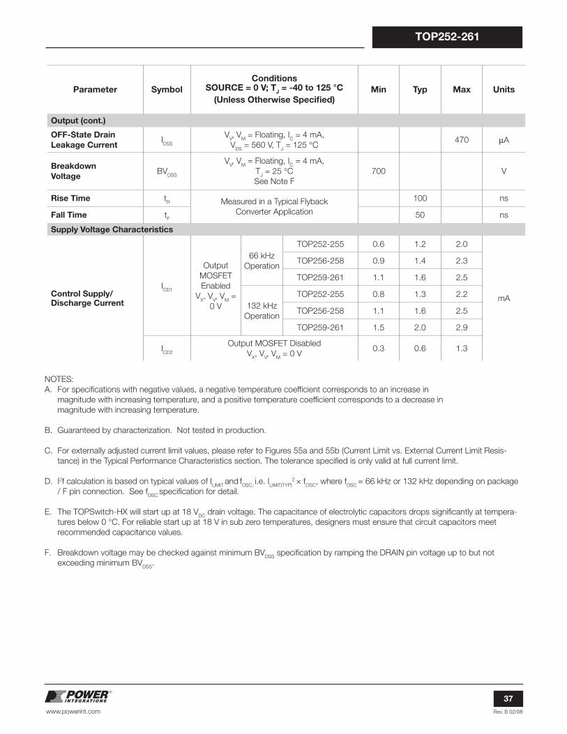
Rev. B 02/08
37
TOP252-261
www.powerint.com
NOTES:
For specifi cations with negative values, a negative temperature coeffi cient corresponds to an increase in
magnitude with increasing temperature, and a positive temperature coeffi cient corresponds to a decrease in
magnitude with increasing temperature.
Guaranteed by characterization. Not tested in production.
For externally adjusted current limit values, please refer to Figures 55a and 55b (Current Limit vs. External Current Limit Resis-
tance) in the Typical Performance Characteristics section. The tolerance specifi ed is only valid at full current limit.
I2f calculation is based on typical values of ILIMIT
and fOSC,
i.e. ILIMIT(TYP)
2 × fOSC
, where fOSC
= 66 kHz or 132 kHz depending on package
/ F pin connection. See fOSC
specifi cation for detail.
The TOPSwitch-HX will start up at 18 VDC
drain voltage. The capacitance of electrolytic capacitors drops signifi cantly at tempera-
tures below 0 °C. For reliable start up at 18 V in sub zero temperatures, designers must ensure that circuit capacitors meet
recommended capacitance values.
Breakdown voltage may be checked against minimum BVDSS
specifi cation by ramping the DRAIN pin voltage up to but not
exceeding minimum BVDSS
.
A.
B.
C.
D.
E.
F.
Parameter Symbol
ConditionsSOURCE = 0 V; T
J = -40 to 125 °C
(Unless Otherwise Specifi ed)
Min Typ Max Units
Output (cont.)
OFF-State Drain
Leakage CurrentIDSS
VV, V
M = Floating, I
C = 4 mA,
VDS
= 560 V, TJ = 125 °C 470 μA
Breakdown
VoltageBV
DSS
VV, V
M = Floating, I
C = 4 mA,
TJ = 25 °C
See Note F
700 V
Rise Time tR Measured in a Typical Flyback
Converter Application
100 ns
Fall Time tF
50 ns
Supply Voltage Characteristics
Control Supply/ Discharge Current
ICD1
Output
MOSFET
Enabled
VX, V
V, V
M =
0 V
66 kHz
Operation
TOP252-255 0.6 1.2 2.0
mA
TOP256-258 0.9 1.4 2.3
TOP259-261 1.1 1.6 2.5
132 kHz
Operation
TOP252-255 0.8 1.3 2.2
TOP256-258 1.1 1.6 2.5
TOP259-261 1.5 2.0 2.9
ICD2
Output MOSFET Disabled
VX, V
V, V
M = 0 V
0.3 0.6 1.3

Rev. B 02/08
38
TOP252-261
www.powerint.com
Figure 51. Duty Cycle Measurement.
Figure 52. CONTROL Pin I-V Characteristic. Figure 53. Drain Current Operating Envelope.
Figure 54. TOPSwitch-HX General Test Circuit.
PI-2039-033001
DRAINVOLTAGE
HV
0 V
90%
10%
90%
t2
t1
D = t1t2
120
100
80
40
20
60
05 6 7 8 9
CONTROL Pin Voltage (V)
CO
NT
RO
L P
in C
urr
ent
(mA
)
1Slope
DynamicImpedance
=
PI-
4737
-061
207
0.8
1.31.21.1
0.90.8
1.0
00 1 2 6 83
Time ( s)
DR
AIN
Cu
rren
t (n
orm
aliz
ed)
PI-
4758
-061
407
4 5 7
0.70.60.50.40.30.20.1
IINIT(MIN)
tLEB (Blanking Time)
PI-4738-020508
5-50 V
5-50 V
S4
40 V
0.1 μF47 μF
470 Ω5 W
TOP254-258 Y, E or M Packages (X and V Pins)
P or G Package (M Pin)
470 Ω
0-300 kΩ
0-60 kΩ
0-60 kΩ
0-300 kΩ
NOTES: 1. This test circuit is not applicable for current limit or output characteristic measurements. 2. For P, G and M packages, short all SOURCE pins together.
D
DSF X
C
V
M
CCONTROL
TOPSwitch-HX
S1 S5
S30-15 V
S2
SG X
CCONTROL
TOP259-261 Y (X and V Pins)
5-50 V
0-300 kΩ
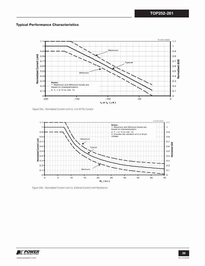
Rev. B 02/08
39
TOP252-261
www.powerint.com
Figure 55a. Normalized Current Limit vs. X or M Pin Current.
Figure 55b. Normalized Current Limit vs. External Current Limit Resistance.
PI-4754-120307
0
0.1
0.2
0.3
0.4
0.5
0.6
0.7
0.8
0.9
1
1.1
-200 -150 -100 -50 0
IX or IM ( μA )
0
0.1
0.2
0.3
0.4
0.5
0.6
0.7
0.8
0.9
1
1.1
Typical
Notes:1. Maximum and Minimum levels are based on characterization;
2. T J = 0 OC to 125 OC
Minimum
Maximum
Nor
mal
ized
Cur
rent
Lim
it
Nor
mal
ized
di/d
t
PI-4755-120307
0
0.1
0.2
0.3
0.4
0.5
0.6
0.7
0.8
0.9
1
1.1
0 5 10 15 20 25 30 35 40 45
RIL ( kΩ )
0
0.1
0.2
0.3
0.4
0.5
0.6
0.7
0.8
0.9
1
1.1Notes:1. Maximum and Minimum levels are based on characterization;
2. T J = 0 OC to 125 OC;3. Includes the variation of X or M pin voltage
Typical
Maximum
Minimum
Norm
aliz
ed C
urre
nt L
imit
Norm
aliz
ed d
i/dt
Typical Performance Characteristics

Rev. B 02/08
40
TOP252-261
www.powerint.com
Typical Performance Characteristics (cont.)
1.1
1.0
0.9-50 -25 0 25 50 75 100 125 150
Junction Temperature ( C)
Bre
akd
ow
n V
olt
age
(No
rmal
ized
to
25
C) PI-
176B
-033
001 1.2
1.0
0.8
0.6
0.4
0.2
0-50 -25 0 25 50 75 100 125 150
Junction Temperature ( C)
PI-
4759
-061
407
Ou
tpu
t F
req
uen
cy(N
orm
aliz
ed t
o 2
5 C
)
1.2
1.0
0.8
0.6
0.4
0.2
0-50 -25 0 25 50 75 100 125 150
Junction Temperature ( C)
PI-
4760
-061
407
Cu
rren
t L
imit
(No
rmal
ized
to
25
C)
1.2
1.0
0.8
0.6
0.4
0.2
0-50 -25 0 25 50 75 100 125 150
Junction Temperature (°C)
PI-
4739
-061
507
Cu
rren
t L
imit
(No
rmal
ized
to
25
°C)
1.2
1.0
0.8
0.6
0.4
0.2
0-50 -25 0 25 50 75 100 125 150
Junction Temperature ( C)
PI-
4761
-061
407
Ove
rvo
ltag
e T
hre
sho
ld(N
orm
aliz
ed t
o 2
5 C
)
1.2
1.0
0.8
0.6
0.4
0.2
0-50 -25 0 25 50 75 100 125 150
Junction Temperature ( C)
PI-
4762
-061
407
Un
der
-Vo
ltag
e T
hre
sho
ld(N
orm
aliz
ed t
o 2
5 C
)
Figure 56. Breakdown Voltage vs. Temperature. Figure 57. Frequency vs. Temperature.
Figure 58. Internal Current Limit vs. Temperature. Figure 59. External Current Limit vs. Temperature with RIL = 10.5 kΩ.
Figure 60. Overvoltage Threshold vs. Temperature. Figure 61. Undervoltage Threshold vs. Temperature.

Rev. B 02/08
41
TOP252-261
www.powerint.com
Typical Performance Characteristics (cont.)
6
4.5
5.5
5
20 100 200 500400300
VOLTAGE-MONITOR Pin Current ( A)
VO
LTA
GE
MO
NIT
OR
Pin
Vo
ltag
e (V
)
PI-
4740
-060
607
3
2.5
3.5
4
1.6
1.0
1.4
1.2
0-200 -150 -50-100 0
EXTERNAL CURRENT LIMIT Pin Current ( A)
EX
TE
RN
AL
CU
RR
EN
T L
IMIT
P
in V
olt
age
(V)
PI-
4741
-110
907
0.4
0.2
0.6
0.8
VX = 1.354 - 1147.5 × IX 1.759 × 10⁶ × (IX)2 with -180 A IX -25 A
6
5
4
3
2
1
0-200 -100 0 100 200 300 400 500
PI-
4742
-021
308
MU
LTI-
FU
NC
TIO
N P
in V
olt
age
(V)
MULTI-FUNCTION Pin Current ( A)
See expandedversion(Figure 63b)
1.2
1.4
1.6
0.4
0.6
0.2
0.8
1.0
0-200 -150 -50-100 0
MU
LTI-
FU
NC
TIO
N P
in V
olt
age
(V)
PI-
4743
-061
407
MULTI-FUNCTION Pin Current ( A)
VM = 1.354 - 1147.5 × IM 1.759 × 10⁶ × (IM)2 with -180 A IM -25 A
1.2
1.0
0.8
0.6
0.4
0.2
0-50 -25 0 25 50 75 100 125 150
Junction Temperature ( C)
PI-
4763
-021
408
CO
NT
RO
L C
urr
ent
(No
rmal
ized
to
25
C)
TOP261 1.62TOP260 1.42TOP259 1.17TOP258 1.00TOP257 0.85TOP256 0.61TOP255 0.42TOP254 0.32TOP253 0.20 TOP252 0.10
Scaling Factors:
1.2
1.0
0.8
0.6
0.4
0.2
0-50 -25 0 25 50 75 100 125 150
Junction Temperature ( C)
PI-
4764
-061
407
On
set
Th
resh
old
Cu
rren
t(N
orm
aliz
ed t
o 2
5 C
)
Figure 62a. LINE-SENSE Pin Voltage vs. Current. Figure 62b. EXTERNAL CURRENT LIMIT Pin Voltage vs. Current.
Figure 63a. MULTI-FUNCTION Pin Voltage vs. Current. Figure 63b. MULTI-FUNCTION Pin Voltage vs. Current (Expanded).
Figure 64. Control Current Out at 0% Duty Cycle vs. Temperature. Figure 65. Maximum Duty Cycle Reduction Onset Threshold
Current vs. Temperature.
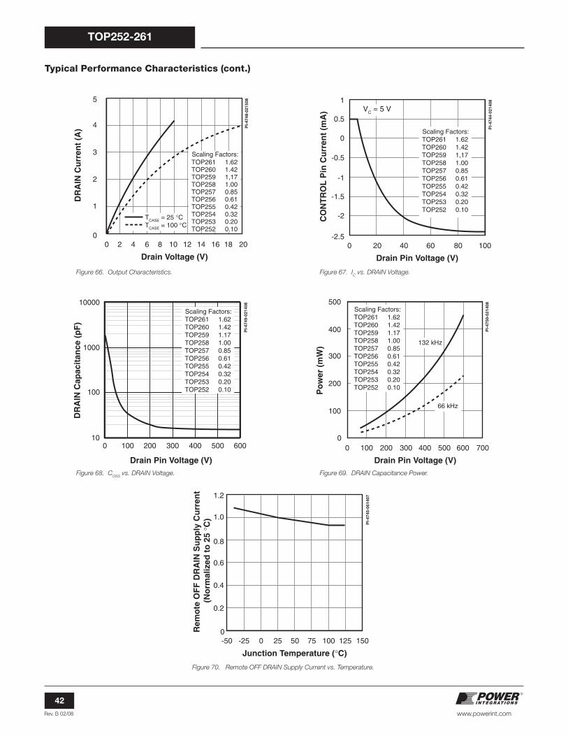
Rev. B 02/08
42
TOP252-261
www.powerint.com
Typical Performance Characteristics (cont.)
1
-0.5
0
0.5
-2.50 20 40 60 80 100
Drain Pin Voltage (V)
CO
NT
RO
L P
in C
urr
ent
(mA
)
PI-
4744
-021
408
-1.5
-2
-1
VC = 5 V
TOP261 1.62TOP260 1.42TOP259 1,17TOP258 1.00TOP257 0.85TOP256 0.61TOP255 0.42TOP254 0.32TOP253 0.20 TOP252 0.10
Scaling Factors:
Figure 66. Output Characteristics. Figure 67. IC vs. DRAIN Voltage.
Figure 68. COSS
vs. DRAIN Voltage. Figure 69. DRAIN Capacitance Power.
Figure 70. Remote OFF DRAIN Supply Current vs. Temperature.
5
00 2 4 6 8 10 12 14 16 18 20
Drain Voltage (V)
DR
AIN
Cu
rren
t (A
) PI-
4748
-021
508
2
1
TCASE = 25 CTCASE = 100 C
4
3TOP261 1.62TOP260 1.42TOP259 1,17TOP258 1.00TOP257 0.85TOP256 0.61TOP255 0.42TOP254 0.32TOP253 0.20 TOP252 0.10
Scaling Factors:
0 100 200 300 400 500 60010
100
1000
10000
PI-
4749
-021
408
Drain Pin Voltage (V)
DR
AIN
Cap
acit
ance
(p
F) TOP261 1.62
TOP260 1.42TOP259 1.17TOP258 1.00TOP257 0.85TOP256 0.61TOP255 0.42TOP254 0.32TOP253 0.20 TOP252 0.10
Scaling Factors:500
400
200
100
300
00 200100 400 500 600300 700
Drain Pin Voltage (V)
Po
wer
(m
W)
PI-
4750
-021
408
132 kHz
66 kHz
TOP261 1.62TOP260 1.42TOP259 1.17TOP258 1.00TOP257 0.85TOP256 0.61TOP255 0.42TOP254 0.32TOP253 0.20 TOP252 0.10
Scaling Factors:
1.2
0.8
1.0
0-50 0-25 5025 10075 125 150
Junction Temperature ( C)
Rem
ote
OF
F D
RA
IN S
up
ply
Cu
rren
t (
No
rmal
ized
to
25
C)
PI-
4745
-061
407
0.2
0.4
0.6

Rev. B 02/08
43
TOP252-261
www.powerint.com
PI-2644-122004
Notes:1. Controlling dimensions are inches. Millimeter dimensions are shown in parentheses. 2. Pin numbers start with Pin 1, and continue from left to right when viewed from the front.3. Dimensions do not include mold flash or other protrusions. Mold flash or protrusions shall not exceed .006 (.15mm) on any side.4. Minimum metal to metal spacing at the package body for omitted pin locations is .068 in. (1.73 mm).5. Position of terminals to be measured at a location .25 (6.35) below the package body.6. All terminals are solder plated.
Y07C
PIN 1 PIN 7
MOUNTING HOLE PATTERN
.050 (1.27)
.150 (3.81)
.050 (1.27)
.150 (3.81)
.050 (1.27)
.050 (1.27)
.100 (2.54)
.180 (4.58).200 (5.08)
PIN 1
+
.010 (.25) M
.461 (11.71)
.495 (12.57)
.390 (9.91).420 (10.67).146 (3.71)
.156 (3.96)
.860 (21.84)
.880 (22.35)
.024 (.61)
.034 (.86)
.068 (1.73) MIN
.050 (1.27) BSC
.150 (3.81) BSC
.108 (2.74) REF
PIN 1 & 7
7° TYP.
PIN 2 & 4
.040 (1.02)
.060 (1.52)
.190 (4.83)
.210 (5.33)
.012 (.30)
.024 (.61)
.080 (2.03)
.120 (3.05)
.234 (5.94)
.261 (6.63)
.165 (4.19)
.185 (4.70)
.040 (1.02)
.060 (1.52)
.045 (1.14)
.055 (1.40)
.670 (17.02) REF.
.570 (14.48) REF.
TO-220-7C

Rev. B 02/08
44
TOP252-261
www.powerint.com
Notes:1. Package dimensions conform to JEDEC specification MS-001-AB (Issue B 7/85) for standard dual-in-line (DIP) package with .300 inch row spacing.2. Controlling dimensions are inches. Millimeter sizes are shown in parentheses.3. Dimensions shown do not include mold flash or other protrusions. Mold flash or protrusions shall not exceed .006 (.15) on any side.4. Pin locations start with Pin 1, and continue counter-clock- wise to Pin 8 when viewed from the top. The notch and/or dimple are aids in locating Pin 1. Pin 3 is omitted.5. Minimum metal to metal spacing at the package body for the omitted lead location is .137 inch (3.48 mm).6. Lead width measured at package body. 7. Lead spacing measured with the leads constrained to be perpendicular to plane T.
.008 (.20)
.015 (.38)
.300 (7.62) BSC(NOTE 7)
.300 (7.62)
.390 (9.91)
.367 (9.32)
.387 (9.83)
.240 (6.10)
.260 (6.60)
.125 (3.18)
.145 (3.68)
.057 (1.45)
.068 (1.73)
.120 (3.05)
.140 (3.56)
.015 (.38)MINIMUM
.048 (1.22)
.053 (1.35).100 (2.54) BSC
.014 (.36)
.022 (.56)
-E-
Pin 1
SEATINGPLANE
-D-
-T-
P08C
DIP-8C
PI-3933-100504
D S .004 (.10)⊕
T E D S .010 (.25) M⊕
(NOTE 6)
.137 (3.48)MINIMUM
Notes:1. Package dimensions conform to JEDEC specification MS-019.2. Controlling dimensions are inches. Millimeter sizes are shown in parentheses.3. Dimensions shown do not include mold flash or other protrusions. Mold flash or protrusions shall not exceed .006 (.15) on any side.4. D, E and F are reference datums.5. Dimensioning and tolerancing conform to ASME Y14.5M-1994.
.008 (.20)
.015 (.38)
.300 (7.62)
.390 (9.91)
.240 (6.10)
.260 (6.60)
10 6
1 5
.200 (5.08) Max
.020 (.51) Min
.367 (9.32)
.387 (9.83)
.120 (3.05)
.140 (3.56)
.030 (.76).040 (1.02)
.070 (1.78) BSC .300 BSC
.300 (7.62).340 (8.64
.014 (.36)
.022 (.56)
.125 (3.18)
.145 (3.68)
-E-
SEATINGPLANE
-D-
P10C
SDIP-10C
PI-4648-041107
F D E.010 (.25) M⊕
-F-
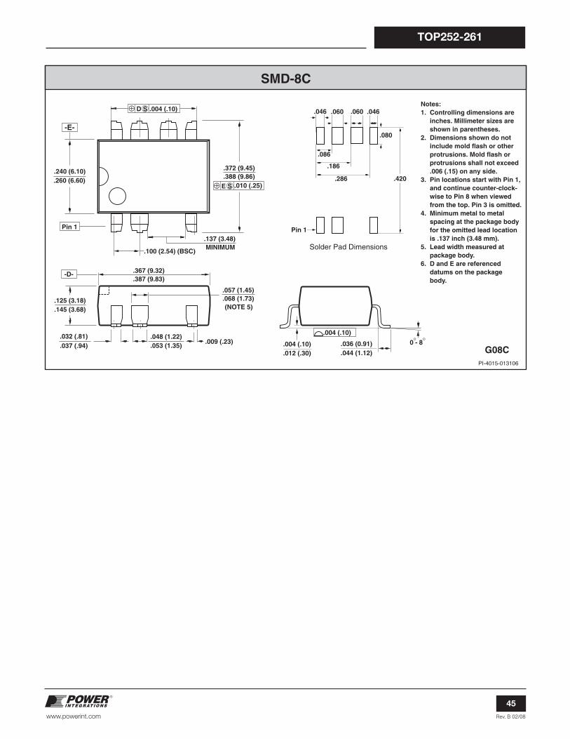
Rev. B 02/08
45
TOP252-261
www.powerint.com
SMD-8C
PI-4015-013106
.004 (.10)
.012 (.30) .036 (0.91) .044 (1.12)
.004 (.10)
0 - ° 8 °
.367 (9.32)
.387 (9.83)
.048 (1.22) .009 (.23)
.053 (1.35) .032 (.81) .037 (.94)
.125 (3.18)
.145 (3.68)
-D-
Notes: 1. Controlling dimensions are inches. Millimeter sizes are shown in parentheses. 2. Dimensions shown do not include mold flash or other protrusions. Mold flash or protrusions shall not exceed .006 (.15) on any side. 3. Pin locations start with Pin 1, and continue counter-clock- wise to Pin 8 when viewed from the top. Pin 3 is omitted. 4. Minimum metal to metal spacing at the package body for the omitted lead location is .137 inch (3.48 mm). 5. Lead width measured at package body. 6. D and E are referenced datums on the package body.
.057 (1.45)
.068 (1.73) (NOTE 5)
E S
.100 (2.54) (BSC)
.372 (9.45) .240 (6.10)
.388 (9.86) .260 (6.60)
.010 (.25)
-E-
Pin 1
D S .004 (.10) ⊕
⊕
G08C
.420
.046 .060 .060 .046
.080
Pin 1
.086
.186
.286
Solder Pad Dimensions
.137 (3.48) MINIMUM

Rev. B 02/08
46
TOP252-261
www.powerint.com
Part Ordering Information
• TOPSwitch Product Family
• HX Series Number
• Package Identifi er
P Plastic DIP-8C
G Plastic SMD-8C
M Plastic SDIP-10C
Y Plastic TO-220-7C
E Plastic eSIP-7C
• Pin Finish
N Pure Matte Tin (Pb-Free) (P, G, M, E and Y Packages)
• Tape & Reel and Other Options
Blank Standard Confi gurations
TL G Package (1000 min/mult.)TOP 258 P N - TL
PI-4917-123107
Notes:1. Dimensioning and tolerancing per ASME Y14.5M-1994. 2. Dimensions noted are determined at the outermost extremes of the plastic body exclusive of mold flash, tie bar burrs, gate burrs, and interlead flash, but including any mismatch between the top and bottom of the plastic body.3. Dimensions noted are inclusive of plating thickness.4. Does not include inter-lead flash or protrusions.5. Controlling dimensions in inches (mm).
0.403 (10.24)0.397 (10.08)
0.325 (8.25)0.320 (8.13)
0.050 (1.27)
FRONT VIEW
2
2
B
A
0.070 (1.78) Ref.
Pin #1I.D.
3
C
0.016 (0.41)Ref.
0.047 (1.19) 0.100 (2.54)
0.519 (13.18)Ref.
0.177 (4.50) Ref.
0.224 (5.69) Ref.
0.118 (3.00)
6× 6×
3A A
0.140 (3.56)0.120 (3.05)
0.021 (0.53)0.019 (0.48)
0.378 (9.60)Ref. 0.019 (0.48) Ref.
0.060 (1.52)Ref.
0.048 (1.22)0.046 (1.17)
0.081 (2.06)0.077 (1.96)
0.207 (5.26)0.187 (4.75)
0.033 (0.84)0.028 (0.71)
0.016 (0.41)0.011 (0.28)
eSIP-7C
10° Ref.All Around
0.020 M 0.51 M C 0.010 M 0.25 M C A B
SIDE VIEW
Section A–A END VIEW
BACK VIEW
0.030 (0.76) Ref.
0.012 (0.30) Ref.Base Metal
3
0.033 (0.84)0.028 (0.71)
0.016 (0.41)0.011 (0.28)
3 4
4

Rev. B 02/08
47
TOP252-261
www.powerint.com
Notes

Revision Notes Date
B Data Sheet Release 02/08
For the latest updates, visit our website: www.powerint.comPower Integrations reserves the right to make changes to its products at any time to improve reliability or manufacturability. Power
Integrations does not assume any liability arising from the use of any device or circuit described herein. POWER INTEGRATIONS MAKES
NO WARRANTY HEREIN AND SPECIFICALLY DISCLAIMS ALL WARRANTIES INCLUDING, WITHOUT LIMITATION, THE IMPLIED
WARRANTIES OF MERCHANTABILITY, FITNESS FOR A PARTICULAR PURPOSE, AND NON-INFRINGEMENT OF THIRD PARTY RIGHTS.
Patent Information
The products and applications illustrated herein (including transformer construction and circuits external to the products) may be covered
by one or more U.S. and foreign patents, or potentially by pending U.S. and foreign patent applications assigned to Power Integrations. A
complete list of Power Integrations patents may be found at www.powerint.com. Power Integrations grants its customers a license under
certain patent rights as set forth at http://www.powerint.com/ip.htm.
Life Support Policy
POWER INTEGRATIONS PRODUCTS ARE NOT AUTHORIZED FOR USE AS CRITICAL COMPONENTS IN LIFE SUPPORT DEVICES OR
SYSTEMS WITHOUT THE EXPRESS WRITTEN APPROVAL OF THE PRESIDENT OF POWER INTEGRATIONS. As used herein:
A Life support device or system is one which, (i) is intended for surgical implant into the body, or (ii) supports or sustains life, and (iii)
whose failure to perform, when properly used in accordance with instructions for use, can be reasonably expected to result in signifi cant
injury or death to the user.
A critical component is any component of a life support device or system whose failure to perform can be reasonably expected to cause
the failure of the life support device or system, or to affect its safety or effectiveness.
The PI logo, TOPSwitch, TinySwitch, LinkSwitch, DPA-Switch, PeakSwitch, EcoSmart, Clampless, E-Shield, Filterfuse, StakFET, PI Expert
and PI FACTS are trademarks of Power Integrations, Inc. Other trademarks are property of their respective companies.
©2008, Power Integrations, Inc.
1.
2.
Power Integrations Worldwide Sales Support Locations
World Headquarters5245 Hellyer Avenue
San Jose, CA 95138, USA.
Main: +1-408-414-9200
Customer Service:
Phone: +1-408-414-9665
Fax: +1-408-414-9765
e-mail: [email protected]
China (Shanghai)Rm 807-808A
Pacheer Commercial Centre,
555 Nanjing Rd. West
Shanghai, P.R.C. 200041
Phone: +86-21-6215-5548
Fax: +86-21-6215-2468
e-mail: [email protected]
China (Shenzhen)Rm A, B & C 4th Floor, Block C,
Electronics Science and
Technology Bldg., 2070
Shennan Zhong Rd,
Shenzhen, Guangdong,
China, 518031
Phone: +86-755-8379-3243
Fax: +86-755-8379-5828
e-mail: [email protected]
GermanyRueckertstrasse 3
D-80336, Munich
Germany
Phone: +49-89-5527-3910
Fax: +49-89-5527-3920
e-mail: [email protected]
India#1, 14th Main Road
Vasanthanagar
Bangalore-560052 India
Phone: +91-80-4113-8020
Fax: +91-80-4113-8023
e-mail: [email protected]
ItalyVia De Amicis 2
20091 Bresso MI
Italy
Phone: +39-028-928-6000
Fax: +39-028-928-6009
e-mail: [email protected]
JapanKosei Dai-3 Bldg.
2-12-11, Shin-Yokomana,
Kohoku-ku
Yokohama-shi Kanagwan
222-0033 Japan
Phone: +81-45-471-1021
Fax: +81-45-471-3717
e-mail: [email protected]
KoreaRM 602, 6FL
Korea City Air Terminal B/D, 159-6
Samsung-Dong, Kangnam-Gu,
Seoul, 135-728, Korea
Phone: +82-2-2016-6610
Fax: +82-2-2016-6630
e-mail: [email protected]
Singapore51 Newton Road
#15-08/10 Goldhill Plaza
Singapore, 308900
Phone: +65-6358-2160
Fax: +65-6358-2015
e-mail: [email protected]
Taiwan5F, No. 318, Nei Hu Rd., Sec. 1
Nei Hu Dist.
Taipei, Taiwan 114, R.O.C.
Phone: +886-2-2659-4570
Fax: +886-2-2659-4550
e-mail: [email protected]
Europe HQ1st Floor, St. James’s House
East Street, Farnham
Surrey GU9 7TJ
United Kingdom
Phone: +44 (0) 1252-730-141
Fax: +44 (0) 1252-727-689
e-mail: [email protected]
Applications HotlineWorld Wide +1-408-414-9660
Applications FaxWorld Wide +1-408-414-9760
..