towards quantitative electrostatic potential mapping of
TRANSCRIPT

General rights Copyright and moral rights for the publications made accessible in the public portal are retained by the authors and/or other copyright owners and it is a condition of accessing publications that users recognise and abide by the legal requirements associated with these rights.
Users may download and print one copy of any publication from the public portal for the purpose of private study or research.
You may not further distribute the material or use it for any profit-making activity or commercial gain
You may freely distribute the URL identifying the publication in the public portal If you believe that this document breaches copyright please contact us providing details, and we will remove access to the work immediately and investigate your claim.
Downloaded from orbit.dtu.dk on: May 08, 2019
Towards quantitative electrostatic potential mapping of working semiconductordevices using off-axis electron holography
Yazdi, Sadegh; Kasama, Takeshi; Beleggia, Marco; Samaie Yekta, Maryam; McComb, David W.;Twitchett-Harrison, Alison C.; Dunin-Borkowski, Rafal E.Published in:ULTRAMICROSCOPY
Link to article, DOI:10.1016/j.ultramic.2014.12.012
Publication date:2015
Document VersionPeer reviewed version
Link back to DTU Orbit
Citation (APA):Yazdi, S., Kasama, T., Beleggia, M., Samaie Yekta, M., McComb, D. W., Twitchett-Harrison, A. C., & Dunin-Borkowski, R. E. (2015). Towards quantitative electrostatic potential mapping of working semiconductor devicesusing off-axis electron holography. ULTRAMICROSCOPY, 152, 10-20.https://doi.org/10.1016/j.ultramic.2014.12.012
1
Towards quantitative electrostatic potential mapping of working 1
semiconductor devices using off-axis electron holography 2
Sadegh Yazdi1,2
, Takeshi Kasama2, Marco Beleggia
2, Maryam Samaie Yekta
2, David W. McComb
1,3, 3
Alison C. Twitchett-Harrison1 and Rafal E. Dunin-Borkowski
2,4 4
1Department of Materials, Imperial College London, London SW7 2AZ, United Kingdom 5
2Center for Electron Nanoscopy, Technical University of Denmark, DK 2800 Lyngby, Denmark 6
3Department of Materials Science and Engineering, The Ohio State University, Columbus, Ohio 7
43210, United States 8
4Ernst Ruska-Centre for Microscopy and Spectroscopy with Electrons and Peter Grünberg Institute, 9
Forschungszentrum Jülich, D-52425 Jülich, Germany 10
11
Abstract 12
Pronounced improvements in the understanding of semiconductor device performance are expected if 13
electrostatic potential distributions can be measured quantitatively and reliably under working 14
conditions with sufficient sensitivity and spatial resolution. Here, we employ off-axis electron 15
holography to characterize an electrically-biased Si p-n junction by measuring its electrostatic 16
potential, electric field and charge density distributions under working conditions. A comparison 17
between experimental electron holographic phase images and images obtained using three-18
dimensional electrostatic potential simulations highlights several remaining challenges to quantitative 19
analysis. Our results illustrate how the determination of reliable potential distributions from phase 20
images of electrically biased devices requires electrostatic fringing fields, surface charges, specimen 21
preparation damage and the effects of limited spatial resolution to be taken into account. 22

2
1) Introduction 23
As semiconductor devices continue to shrink, so variations in the placement of small numbers of 24
dopant atoms can drastically change electrostatic potential distributions in the devices’ active regions 25
and affect their electrical and optical properties1. Existing methods for introducing dopants are not yet 26
sufficiently controllable, while electrostatic potential measurement techniques are not yet precise 27
enough for the development and understanding of future device generations2. Comprehensive 28
feedback from a quantitative potential measurement technique is crucial for parameter optimization in 29
device modeling, ideally in three dimensions with high spatial resolution and high precision. 30
The technique of off-axis electron holography in the transmission electron microscope (TEM) 31
promises to achieve the required spatial resolution and precision for potential measurement in two 32
dimensions3 and can be combined with electron tomography for three-dimensional measurements
4. 33
Moreover, by carrying out electron holography on a semiconductor device that is electrically biased in 34
situ in the TEM, it is in principle possible to map the electrostatic potential distribution of a device 35
under working conditions, thereby providing additional information for the optimization of device 36
design and fabrication. 37
An off-axis electron hologram is an interference pattern created by overlapping part of the electron 38
wave that has passed unperturbed through vacuum (the “reference wave”) with another part of the 39
electron wave that has passed through the sample (the “object wave”). The resulting interference 40
pattern encodes the phase difference between the reference and object waves, which can then be 41
reconstructed, e.g., with a standard FFT-based algorithm5. Provided that the reference beam is not 42
perturbed by the presence of the specimen, that the specimen is not magnetic and that the effect of 43
dynamical diffraction on the phase shift is negligible, the reconstructed phase difference can be 44
written in the form: 45
𝜑(𝑥, 𝑦) = 𝐶𝐸 ∫ 𝑉(𝑥, 𝑦, 𝑧)𝑑𝑧+∞
−∞
(1)
where CE is a constant that depends on the energy of the electron beam (CE = 8.56 mrad V-1
nm-1
at 46
120 keV), V is the electrostatic potential and z is the electron beam direction. If the electrostatic 47
potential distribution is constant in the electron beam direction (i.e., it has no z-dependence) and 48

3
limited to the interior of the specimen (i.e., there are no fringing fields), then Eq. (1) can be simplified 49
to: 50
𝜑(𝑥, 𝑦) = 𝐶𝐸𝑉(𝑥, 𝑦)𝑡(𝑥, 𝑦), (2)
where 𝑡 is the specimen thickness. Therefore, if the specimen thickness 𝑡(𝑥, 𝑦) is known and the 51
phase shift 𝜑(𝑥, 𝑦) is measured using electron holography, then in principle the electrostatic potential 52
distribution across the specimen can be mapped. However, despite the fact that the phase shift can be 53
measured with high sensitivity (better than 1 mrad6) using electron holography, the interpretation of 54
phase images in terms of electrostatic potential distributions requires several factors to be taken into 55
account. 56
As the phase shift is highly sensitive to specimen thickness, any small thickness variations can be 57
misinterpreted as electrostatic potential variations. For example, a 3 nm step in thickness (e.g., due to 58
preferential milling) in a Si specimen of thickness 300 nm can be misinterpreted as a built-in potential 59
difference of 0.12 V (at 120 kV accelerating voltage). A possible workaround to bypass this problem 60
and to avoid possible misinterpretation is to electrically bias the specimen, since, to a first 61
approximation, the phase variation across a p-n junction changes with applied voltage, whereas the 62
contribution to the phase shift due to specimen thickness variations remains unchanged. 63
Changes in mean inner potential (MIP) across heterojunctions must also be taken into account. Steps 64
in phase across heterojunctions measured using electron holography depend on both the difference in 65
MIP and the dopant potential profile across each junction, as well as on any local redistribution of 66
charge that may be present at each interface in the sample. Differences in MIP can therefore be 67
misinterpreted as dopant potentials, or vice versa. Because MIPs are unchanged by external voltages, 68
it should again be possible to avoid such misinterpretation by measuring phase steps across 69
heterojunctions under different electrical biasing conditions. Similarly, the effects of diffraction 70
contrast on the phase shift can be misinterpreted as changes in dopant potential and can be removed 71
by electrical biasing, so long as the contribution to the phase from diffraction contrast is unaffected by 72
the applied electrical bias. 73

4
The measured potential may also be affected by electrical charging of the specimen in the presence of 74
electron beam irradiation due to the emission of secondary electrons and the generation of electron-75
hole pairs in the specimen. The presence of electrical contacts close to the region of interest is 76
expected to help to restore any charge imbalance resulting from secondary electron emission from the 77
specimen7. Electrical contacts can also be used to measure electron beam induced current (EBIC)
8 78
and, in this way, to provide information about electron-hole pair generation. 79
The fact that dopant potentials are, in general, much smaller than mean inner potentials, means that a 80
measurement with 0.1 V sensitivity in Si, which has a mean inner potential of ∼12 V, requires a 81
signal to background ratio of better than 1% (to measure a 0.1 V dopant potential on a 12 V 82
background). The ability of electron holography to detect variations in dopant potential can therefore 83
be improved by the application of an applied electrical bias. 84
For all of these reasons, in situ electrical biasing of semiconductor devices in the TEM is expected to 85
provide a valuable solution to many of the issues that need to be overcome when converting electron 86
holographic phase images into electrostatic potential maps, as well as providing an opportunity to 87
characterize semiconductor devices under working conditions. 88
Previous electron holography studies of electrically biased p-n junctions have shown only qualitative 89
agreement between experimental results and theory9–12
. For example, researchers at the University of 90
Bologna demonstrated electrical leakage fields (fringing fields) from an electrically biased p-n 91
junction into vacuum, as expected on the basis of electrostatics10
. They also showed that the fringing 92
fields increase in magnitude with applied reverse bias13
. Subsequently, scientists from Cambridge 93
demonstrated a linear increase of the step in phase across a Si p-n junction with applied reverse bias in 94
a focused ion beam (FIB) prepared specimen14
. 95
Despite qualitative agreement between experiment and theory, the quantitative interpretation of such 96
experimental results reveals large discrepancies. Measured fringing fields are considerably smaller 97
than expected15
, while electrostatic potentials, electric fields, charge densities and dopant 98
concentrations inferred from phase images are almost always significantly lower than predicted 99
values. In addition, measured charge densities across p-n junctions have been reported to depend on 100

5
applied bias, while theory predicts that their magnitude should remain constant, as the depletion layer 101
width increases with applied reverse bias16
. Although electron beam irradiation and specimen 102
preparation damage have been blamed for these discrepancies in the literature17,18
, their origin is not 103
yet fully understood. Here, we address these issues quantitatively by measuring the electrostatic 104
potential, electric field and charge density across a Si p-n junction from electron holograms acquired 105
under different electrical biasing conditions and by comparing the measurements with simulations. 106
2) Experiment 107
2.1) Experimental Details 108
An abrupt symmetrical Si p-n junction comprising a 4-µm-thick As-doped (n-type) layer grown 109
epitaxially onto a (100) oriented B-doped (p-type) substrate using molecular beam epitaxy was 110
provided by OKMETIC19
. The electrically active dopant concentration was determined using a four-111
point-probe measurement to be 6×10¹⁸
cm-3
on each side of the junction, which corresponds to an 112
expected built-in potential of 1.02 V across the junction. In order to electrically bias the p-n junction 113
in situ in the TEM, a 1.5 mm × 1.5 mm × 100 µm cleaved piece of the wafer was clamped between 114
two electrical contacts in a cartridge-based single tilt biasing holder20
. A parallel-sided electron 115
transparent membrane was then micromachined at one corner of the cleaved wedge using a 30 keV 116
focused ion beam (FIB)21
. The length of the electron transparent membrane was kept as short as 1 µm, 117
while the rest of the specimen was significantly thicker, to minimize charging during the holography 118
observation. At the final stage of specimen preparation, at a thickness of approximately 600 nm, low 119
keV cleaning was carried out using 2 keV FIB milling to reduce the effects of specimen surface 120
damage and Ga implantation. The crystalline thickness of the membrane was determined to be 121
550±10 nm using convergent beam electron diffraction (CBED) in a two beam condition. The 122
applied voltage across the junction was varied between 0 and 2 V reverse bias in intervals of 0.2 V. 123
At each voltage, both an object off-axis electron hologram and a vacuum reference electron hologram 124
were recorded. The holograms were acquired in an FEI Titan 80-300 TEM operated at 120 kV in 125
Lorentz mode. By setting the biprism voltage to 70 V and the magnification to 18600×, holograms 126

6
with a visible overlap region of ∽0.6×2 µm2 at 6 pixels per fringe could be acquired on a 2k×2k 127
charge-coupled device (CCD) camera, with a holographic interference fringe spacing of 4.6 nm and 128
fringe visibility of 20% for an acquisition time of 16 s. The p-n junction was oriented exactly edge-on 129
with respect to the electron beam by tilting the specimen to the central line of the 040 Kikuchi band, 130
at a specimen tilt angle of 5.2o from the <001> zone axis. 131
2.2) Experimental Results 132
Representative reconstructed phase and amplitude images, obtained by applying a mask of radius 1/14 133
nm-1
to the sideband in the Fourier transform of the hologram for 0 V applied bias, are shown in Figs. 134
1(a) and (b), respectively. The p- and n- regions are clearly visible in the phase image. No diffraction 135
contrast can be seen in the amplitude image at this specimen orientation, suggesting that dynamical 136
diffraction does not affect the phase step across the p-n junction significantly. 137
The step in phase across the junction (Fig. 1(c)) is plotted as a function of applied bias voltage in Fig. 138
1(d), showing the expected linear relationship between the step in potential and applied bias across the 139
junction for a reverse biased p-n junction. It is immediately apparent from this plot that the FIB-140
prepared p-n junction specimen responds to the applied voltage, with the potential step across the 141
junction increasing with applied reverse bias. Assuming that i) the electrically active specimen 142
thickness is the same on both the n- and the p- sides of the junction21
, ii) the phase shift due to the 143
junction is contained within the specimen and iii) the applied bias is dropped fully across the junction 144
and not elsewhere on the specimen or holder, then the slope and intercept of the graph shown in 145
Fig. 1(d) provide values for the electrically active specimen thickness and the built-in potential across 146
the junction of 500±10 nm and 0.9±0.1 V, respectively, by using the expressions 147
{
∆φ = 4.35Vapp + 3.92
∆φ = CEtVapp + CEtVbi
⟹ t = 500 ± 10 nm, Vbi = 0.9 ± 0.1 V
(3)
where Δφ, Vapp and Vbi are the phase step, applied reverse bias voltage and built-in potential across the 148
p-n junction, respectively. Fig. 1(e) shows representative potential, electric field and charge density 149

7
distributions extracted from the dashed box marked in Fig. 1(a) for different values of applied reverse 150
bias, assuming the full 550 nm crystalline thickness of the specimen (measured using CBED) when 151
converting the phase images into maps of electrostatic potential V, electric field E and charge density 152
ρ using the expressions: 153
𝑉(𝑥, 𝑦) = 𝜑(𝑥, 𝑦)/𝐶𝐸𝑡 (4)
𝐸(𝑥, 𝑦) = −∇. 𝑉(𝑥, 𝑦)
𝜌(𝑥, 𝑦) = −𝜀Siε0∇2𝑉(𝑥, 𝑦)
(5)
(6)
where εSi=11.7 and ε0= 8.85×10⁻¹² F/m. 154
The difference between the crystalline specimen thickness measured using CBED and the electrically 155
active specimen thickness inferred from the step in phase plotted as a function of applied voltage is 156
50±10 nm, suggesting that there is a 25±5 nm crystalline layer on each surface of the specimen that is 157
depleted due to a combination of electrical surface states (i.e., surface depletion) and FIB damage22
. 158
The thickness of the depleted and inactive crystalline surface layer has been widely assumed in the 159
literature to be the primary explanation for low values of steps in phase obtained from electron 160
holography results23–27
. 161
The measured built-in potential, 0.9±0.1 V, is just in agreement with the expected theoretical value of 162
1.02 V, while the slope of Fig. 1(d) can be explained by considering an electrically dead layer of 163
thickness 50±10 nm28
. However, there are other discrepancies in the experimental measurements, 164
which are not consistent with this explanation alone. In Fig. 2, experimental electric field and charge 165
density profiles obtained from Fig. 1(e) are compared with classical one-dimensional solutions of the 166
Poisson equation for an abrupt symmetrical Si p-n junction with the measured dopant concentration of 167
6×10¹⁸
cm-3
. Although the general trend in the experimental data is consistent with the simulations, 168
with the depletion width and maximum electric field increasing with applied reverse bias, there are 169
large differences between the magnitudes of the experimental and simulated values. The electric fields 170
measured using electron holography are only about 15% of the simulated values, whether or not the 171
thickness of the electrically inactive surface layer is taken into account, while the measured charge 172

8
densities are more than an order of magnitude lower than the expected value of 6×10¹⁸
cm-3
. In 173
addition, the experimentally measured depletion regions are asymmetrical in the plots of E and ρ and 174
approximately 5 to 10 times wider than the simulated widths, with the measured charge density 175
increasing with reverse bias voltage instead of remaining constant. In contrast to reports in the 176
literature that electrical biasing can reactivate some of the dopants that have been deactivated by 177
specimen preparation (due to Joule heating)12
, in the present study we measured the same charge 178
density at 0 V after many biasing cycles. 179
In contrast to previous reports29
, the surface of the present FIB-prepared specimen is not an 180
equipotential. The experimental phase images are shown in Fig. 3 in the form of eight-times-amplified 181
phase contours and illustrate the presence of fringing fields in the vacuum region outside the 182
specimen, which change with applied reverse bias. The phase shift in the vacuum region along the 183
specimen edge, within the field of view, is greater than 9 rad at 2 V reverse bias. It is important to 184
note that the position of the fringing field is not aligned with the junction position within the 185
specimen, but is shifted slightly towards the p-side of the junction. 186
The leakage of the electric field into the vacuum region has two consequences for off-axis electron 187
holography. First, the assumption that the reference wave is not influenced by the electrostatic 188
potential of the specimen is not strictly valid, and this perturbation needs to be taken into account in 189
the interpretation of the recorded phase images. Second, the presence of the fringing field above and 190
below the specimen needs to be considered. 191
In the following section, by means of numerical simulations, we investigate the role of i) finite spatial 192
resolution, ii) fringing fields, and iii) surface charge on the determination of charge density from 193
electron holographic phase images. 194

9
3) Simulations 195
3.1) Limited spatial resolution 196
One important factor that needs to be considered when calculating charge densities from electrostatic 197
potential maps that have been extracted from phase images is the smoothing of the potential 198
distribution as a result of the finite spatial resolution of the experimental measurements. The effect of 199
limited spatial resolution (14 nm, as dictated by the size of the mask used in reconstructing the phase 200
image) on the charge density distribution extracted from a phase image is illustrated in Fig. 4. In this 201
figure, the theoretical potential distribution across an abrupt Si p-n junction with a dopant 202
concentration of 6×10¹⁸
cm-3
is convoluted with a Gaussian point spread function (with a 14 nm 203
standard deviation) and the charge density is then calculated from its second derivative. Fig. 4(a) 204
shows calculated (theoretical) and smoothed potential profiles across the p-n junction for 0 and 2 V 205
reverse bias. The limited spatial resolution has no effect on the measurement of the magnitude of the 206
potential step across the junction if the measurement can be performed sufficiently far from the 207
position of the junction. However, the potential profile becomes smoother as a result of the limited 208
spatial resolution, resulting in a decrease in the charge density and an increase in the depletion width 209
inferred from the second derivative of the potential profile. For example, the apparent charge density 210
in Fig. 4(b) decreases from 6×10¹⁸
cm-3
to 1×10¹⁸
cm-3
at 0V bias, while the depletion width increases 211
from 20 to 70 nm. 212
The effect of limited spatial resolution on the inferred charge density is not the same for different 213
applied reverse bias voltages. For a larger reverse bias, the curvature of the potential profile is 214
influenced less strongly by the limited spatial resolution, resulting in an apparent increase in charge 215
density in Fig. 4(b), calculated from the second derivatives of the smoothed potential profiles, with 216
applied reverse bias. 217
3.2) Fringing fields 218
Three-dimensional (3D) simulations of electrostatic potentials within and around TEM specimens 219
containing p-n junctions were carried out using the commercially available device simulator ATLAS 220

10
by Silvaco30
. By solving Poissonʹs equation, the electrostatic potential was calculated inside a 500-221
nm-thick parallel-sided specimen containing an abrupt symmetrical Si p-n junction for a dopant 222
concentration of 6×10¹⁸
cm-3
, as well as in a 750-nm-thick vacuum region above and below the 223
specimen and in a 700-nm-thick vacuum region to the side of the specimen. A representative 224
simulated 3D potential distribution is shown in Fig. 5 (a) for an applied bias of 0 V. This figure shows 225
only half of the simulated volume, which continues along the z-axis on the opposite side of the xy 226
plane. The 750-nm-thick vacuum region above and below the specimen is large enough for the 227
electrostatic potential variation to reach a value close to zero at the edge of the simulated volume. In 228
order to apply an electrical bias in the simulations, electrical contacts were considered on the n- and p- 229
sides of the specimen at y = 0 and 1 µm in Fig. 5 (a), respectively. When solving Poissonʹs equation, 230
the difference between the normal components of the respective electric displacements was assumed 231
to be equal to surface charge densities (Neumann boundary conditions) at the positions of the planes 232
with no electrical contacts. At the electrical contacts, a fixed surface potential, fixed electron 233
concentrations and fixed hole concentrations (Dirichlet boundary conditions) were used as boundary 234
conditions. These boundary conditions for the electrical contacts were chosen because experimentally 235
the electrical contacts are over 1 mm away from the region of interest and therefore the drop in 236
voltage across the electrical contacts and its consequent fringing fields do not affect the holography 237
observation. The boundary condition used here for the electrical contacts result in no drop in the 238
electrostatic potential in the semiconductor close to the electrical contacts. In order to investigate the 239
effect of fringing fields on the projected potential, the specimen surface was assumed to have a 240
negligible surface state density in the simulations. The phase shift that the electron beam experiences 241
as it passes through the 3D potential distribution was calculated by integrating the electrostatic 242
potential along the electron beam direction (the z-axis in Fig. 5(a)) and then multiplying the projected 243
potential by the constant CE, according to Eq.1. The perturbation of the reference wave by the fringing 244
field was also considered when calculating the simulated phase images, using an overlap width of 245
500 nm (similar to that measured experimentally). The mean inner potential of Si (∼12 V) was not 246
included in the present simulations, but should have no effect on the calculated electric field and 247

11
charge density, since it simply adds a constant to the electrostatic potential inside the specimen 248
relative to that in vacuum. 249
A representative simulated phase image and corresponding eight-times-amplified phase contours are 250
shown before and after considering the perturbation of the reference wave for an applied reverse bias 251
of 0 V in Figs. 5(b) and (c), respectively. The profiles in Fig. 5(d) represent phase profiles across the 252
junction at 0 V (a, b and c) and 2 V (aʹ, bʹ and cʹ) reverse bias. In this figure, the profiles marked (a) 253
and (aʹ) show the phase change across the junction within the specimen without considering the 254
effects of fringing fields, those marked (b) and (bʹ) show the entire phase change across the junction, 255
including the fringing fields above and below the specimen, while those marked (c) and (cʹ) show the 256
phase profiles after including the effect of the perturbed reference wave. The difference between 257
profiles (cʹ) and (aʹ) shows how much the fringing fields and the perturbed reference wave are 258
predicted to contribute to the phase shift of the electron beam at 2 V reverse bias. The phase step 259
across the junction in this 500-nm-thick specimen is predicted to increase by approximately a factor of 260
three when the contributions to the phase shift from fringing fields above and below the specimen and 261
the perturbed reference wave are considered. Profiles (b) and (bʹ) show that the presence of fringing 262
fields above and below the specimen can introduce a difference in slope in the phase profiles between 263
the p- and n-side of the junction, as well as resulting in a larger phase difference between the p- and n-264
side further from the junction. This difference in slope increases with applied reverse bias. By taking 265
the perturbation of the reference wave into account (profiles (c) and (cʹ) in Fig. 5(d)), the phase step 266
across the junction decreases slightly. However, the profiles also become less flat and the slope of the 267
phase profile on the p- and n- side changes such that further from the junction the phase difference 268
between the p-side and n-side decreases, when compared to that measured close to the junction. 269
In Fig. 5(e), the calculated phase step across the junction is shown before considering the effects of 270
fringing fields and the perturbed reference wave (black triangles), after considering the contribution to 271
the phase shift due to fringing fields above and below the specimen but without considering the 272
perturbed reference wave (blue circles), and after taking the effect of the perturbed reference wave 273
into account (red squares), plotted as a function of applied reverse bias. It can be seen that the 274

12
presence of fringing fields does not affect the linear relationship between the phase step and the 275
applied reverse bias. Although the phase step increases linearly with applied reverse bias in all three 276
cases, the slope and intercept of the fitted lines (shown in the figure) are different. Without 277
considering fringing fields, the intercept of the fitted line represents the product of the specimen 278
thickness, the built-in potential and the constant CE (Eq. 3). After including the contribution to the 279
phase shift from fringing fields above and below the specimen, both the intercept and the slope of the 280
fitted line increase. The values then decrease only slightly when perturbation of the reference wave is 281
taken into account. An important point to note is that the fringing fields do not change the intercept-282
to-slope ratio, which provides a measure of the built-in potential across the junction. This means that 283
the built-in potential extracted from the plot of phase step versus applied reverse bias is not sensitive 284
to the presence of fringing fields. This conclusion can also be reached by analytical calculations31
. 285
In contrast to the experimental observations, when the effects of fringing fields are included in the 286
simulations, the inferred electric fields and charge densities increase significantly when compared to 287
calculations for no fringing fields. The same processing steps were applied to the simulations as to the 288
experimental phase images to obtain the difference electric field and charge density distributions 289
shown in Figs. 5(f) and (g) for different applied bias voltages. For example, the electric field profile 290
shown in Fig. 5(f) for a 2 V reverse bias is the difference between the electric fields calculated from 291
phase profiles (cʹ) and (aʹ). The electric fields and charge densities contributed by the fringing fields 292
show the same trend as the electric fields and charge densities across the p-n junction in response to 293
applied reverse bias, but their magnitudes are larger than those shown in Figs. 2(b) and (d). For 294
example, the maximum electric field at 2 V reverse bias determined from the simulated phase image 295
including the effects of fringing fields (profile (cʹ) in Fig. 5(d)) is 3800 kV/cm, which is the sum of 296
the electric field across the junction (1600 kV/cm) at this applied voltage and the contribution from 297
the presence of fringing fields (2200 kV/cm). 298
The simulations show that, if perfect surfaces with no surface states and damage are assumed for a p-n 299
junction specimen, then the contribution from fringing fields to the phase step across the junction is 300
predicted to be larger than that caused by the p-n junction within the specimen. In contrast, the 301

13
presence of fringing fields does not have a severe effect on the measurement of the depletion width, as 302
the depletion widths in Figs. 5(f) and (g) are approximately in agreement with those in Figs. 2(b) and 303
(d). The built-in potential extracted from the phase step versus applied voltage plot is also not 304
affected significantly by the fringing fields. 305
3.3) Positive surface charge 306
In an attempt to investigate the effect of surface states and secondary electron emission on the 307
measurement of electrostatic potentials using off-axis electron holography, the above 3D electrostatic 308
potential simulation was repeated for the same p-n junction specimen, in the same geometry, but 309
including a uniform positive surface charge on its surfaces. 310
The origin of surface states in a FIB-prepared TEM specimen could be a combination of surface 311
termination, ion beam damage and high-energy electron beam irradiation28,32
. Regardless of the 312
origin, the overall effect of surface states in the presence of electron beam irradiation is likely to result 313
in the presence of positive surface charge on the specimen surfaces. Since few primary electrons are 314
absorbed by a TEM specimen when compared with the number of emitted secondary electrons, it is 315
expected that in the absence of good electrical conductivity on the specimen surfaces they will charge 316
positively33,34
. It is difficult to measure the surface charge density independently. However, we 317
assume a positive surface charge density of 8×10¹²
e.c. (electron charges)/cm2 on all three surfaces of 318
the specimen (top, bottom and edges) in our simulation, based on a comparison between simulated 319
phase profiles in the vacuum region and our experimental electron holographic phase images. 320
Simulated phase profiles for different uniform surface charge densities between 1×10¹²
and 1×10¹³
321
e.c./cm2 in intervals of 1×10
12 e.c./cm
2 were compared with a corresponding phase profile taken along 322
the specimen edge in the vacuum region from the experimental phase image recorded at 0 V bias. The 323
closest match between the experimental and simulated phase profile in the vacuum region at 0 V bias 324
was obtained for a surface charge density of 8×10¹²
e.c./cm2. For higher surface charge densities, the 325
fringing fields disappeared completely, while for lower surface charge densities much stronger 326
fringing fields than those measured experimentally appeared in the vacuum region. As a result of 327

14
assuming a positive surface charge density of 8×10¹²
e.c./cm2, the specimen surfaces on the p-side 328
became inverted to have n-type character. Assuming the depletion approximation32
, such a charge 329
density would result in a surface depletion width of approximately 11 nm and a surface potential 330
difference of approximately 0.6 V on the p-side of the specimen, far from the junction. The strong 331
inversion on the p-side, when the electron concentration at the surface is equal to the dopant 332
concentration in the bulk32
, occurs in this specimen if a positive surface charge density of 333
approximately 1018
e.c./cm2 is assumed on the specimen surface, resulting in a maximum surface 334
depletion width of approximately 15 nm35
. For the purpose of the simulations, the surface charge was 335
considered to be embedded in a 2 nm oxide layer on the specimen surface. The 3D potential 336
distribution obtained from such a simulation is shown in Fig. 6(a). The phase image determined from 337
the simulated potential distribution, as well as corresponding eight-times-amplified phase contours, 338
are shown in Fig. 6(b), taking into account the perturbed reference wave. From Figs. 6(a) and 5(a), it 339
can be seen that the presence of positive surface charge decreases the leakage of electric fields into the 340
vacuum region, with the electrostatic potential variation in the vacuum region in Fig. 6(a) now limited 341
to the proximity of the specimen surfaces when compared to Fig. 5(a). The fringing fields are not only 342
weaker, as can be seen in the eight-times-amplified phase contours shown in Fig. 6(b), but they are 343
also not aligned with the junction position within the specimen in the presence of surface charge. 344
The calculated phase step across the junction in the presence of surface charge is plotted in Fig. 6(c) 345
as a function of applied reverse bias. The phase steps marked with red squares are calculated from the 346
entire simulated volume, whereas the phase steps marked with green diamonds and blue triangles 347
show the contributions from the fringing fields in the vacuum region and the potential variation within 348
the specimen, respectively. At 0 V bias, the calculated phase step associated with the potential 349
variation within the specimen is larger than that from the fringing fields, while at 2 V reverse bias the 350
opposite is the case. 351
Figs. 6(d) and (e) show electric fields and charge densities, respectively, calculated from the phase 352
shift caused only by fringing fields, as in Figs. 5(f) and (g). The electric fields and charge densities 353
calculated from the phase shift determined from the entire simulated volume are shown in Figs. 6(f) 354

15
and (g), respectively. The electric fields and charge densities caused by the fringing fields alone are 355
significantly smaller now that positive charge is included on the specimen surface. Both the electric 356
field and the charge density are asymmetrical in the presence of surface charge, with a lower inferred 357
charge density on the p-side than on the n-side. The inferred charge density increases with applied 358
reverse bias in the presence of surface charge, whereas it does not change with applied bias if no 359
surface charge is included (Fig. 5(g)). The depletion width is also wider in the presence of surface 360
charge. For example, in Fig. 6(g), the depletion width is approximately 80 nm at 2 V reverse bias, 361
whereas in the absence of surface charge it is below 50 nm (Figs. 2(b) and 5(g)). 362
4) Discussion and Summary 363
In the experimental section of this paper, it was shown that a Si p-n junction specimen prepared using 364
FIB milling responds to an applied electrical bias. In qualitative agreement with theory, the potential 365
step, electric field and depletion width across the junction, measured from electron holographic phase 366
images, increase with applied reverse bias. However, instead of remaining constant, the measured 367
charge density increases with applied reverse bias. In contrast to previous reports, but in agreement 368
with theory, fringing fields are observed in the vacuum region close to the specimen edge. The 369
fringing fields increase in magnitude with applied reverse bias. 370
Quantitative comparisons between the experimental results and classical one-dimensional solutions of 371
the Poisson equation for an abrupt Si p-n junction reveal more discrepancies than agreement. 372
Although the built-in potential determined from a plot of phase step versus applied reverse bias is 373
approximately in agreement with the value expected from theory, the electrically active specimen 374
thickness determined from this plot is 50 nm smaller than the crystalline thickness of the specimen 375
measured using CBED. Although one can explain this discrepancy by assuming an electrically 376
inactive crystalline layer on the top and bottom surfaces of the specimen, the presence of fringing 377
fields means that they need to be considered to interpret the measured phase step across the junction. 378
More significantly, the measured electric fields and charge densities are 85% and an order of 379
magnitude smaller than the expected values, respectively, while the measured depletion widths are too 380

16
high by ~300%, the measured charge density is asymmetrical and the fringing fields are not aligned 381
with the position of the junction within the specimen. These discrepancies cannot be explained by the 382
assumption of a simple electrically inactive layer on the top and bottom surfaces of the specimen. 383
In the simulation section, we investigated the effects of limited spatial resolution, fringing fields and 384
surface charge on the electron holography measurements. Simulations presented in this paper did not 385
account for all of the discrepancies, particularly the large depletion width measured experimentally. 386
Limited spatial resolution smooths the potential distribution and results in a lower electric field, a 387
lower charge density and a larger depletion width determined from the projected potential profile. As 388
the effect of limited spatial resolution on the potential step across a p-n junction is smaller for a larger 389
applied reverse bias, a larger charge density is then inferred. Limited spatial resolution is likely to be 390
part of the explanation for the low values of measured electric field and charge density and the large 391
values of depletion width, both in the present study and in other reports16
. However, neither the full 392
extent of the discrepancies nor the asymmetrical charge density profiles can be explained by limited 393
spatial resolution alone. For studying modern nanoscale devices, which was not the aim of this work, 394
a large field of view is not necessary and therefore spatial resolution is not a limiting factor. 395
If the specimen surfaces are assumed to be ideal, with negligible surface states and defects, then 396
electric fields are predicted to leak out from the p-n junction into vacuum and to generate strong 397
fringing fields that can affect the phase image significantly. Our simulations show that the phase shift 398
caused by fringing fields can then be about two times larger than that caused by the potential variation 399
inside a 500-nm-thick specimen containing a symmetrical abrupt Si p-n junction with a dopant 400
concentration of 6×10¹⁸
cm-3
. When calculating electric field and charge density distributions from 401
phase images, the contribution from the phase shift caused by the fringing fields can then be larger 402
than that originating from the interior of the specimen. However, the determination of the built-in 403
potential from the intercept to slope ratio of a plot of phase step versus applied reverse bias is not 404
affected significantly by the fringing fields in the absence of surface charges. When compared with 405
this simulation, significantly weaker fringing fields are observed experimentally, suggesting that the 406
surfaces of TEM specimens in the presence of electron irradiation cannot be assumed to have 407

17
negligible surface state concentrations. In modern devices, in which dopant concentrations can reach a 408
few percent, the fringing fields are expected to be stronger. 409
Simulations incorporating positively charged specimen surfaces were used to model the effects of 410
secondary electron emission during electron irradiation. In order to reproduce the phase shift in the 411
vacuum region close to the specimen edge measured experimentally at 0 V bias, a uniform positive 412
surface charge of 8×10¹²
e.c./cm2 had to be included on the specimen surfaces in the simulation. 413
When compared with simulations for ideal specimen surfaces, the presence of surface charges 414
resulted in weaker fringing fields, lower electric fields, smaller charge densities and wider depletion 415
widths. Moreover, the calculated electric fields and charge densities in the presence of surface charges 416
were asymmetrical, the inferred charge densities increased with applied reverse bias and the fringing 417
fields in vacuum close to the specimen edge were shifted slightly. These observations are all in 418
qualitative agreement with the experimental measurements, suggesting that the presence of positive 419
surface charge on the TEM specimen surface is one of the reasons behind the discrepancies seen 420
between our experimental results and initial simulations. 421
The quality of FIB-prepared surfaces directly affects the strength of fringing fields and is likely to be 422
the reason for the absence of fringing fields in previous studies. It is therefore necessary to develop a 423
standard FIB-based specimen preparation recipe that provides reproducible surfaces and a 424
corresponding electrostatic potential model that predicts the effect of such surface conditions on the 425
electrostatic potential distribution inside and outside the specimen. 426
In conclusion, the discrepancies between experiment and theory seen in electron holographic studies 427
of semiconductor devices are likely to have four different origins: 1) the failure of the dopant potential 428
model used for bulk samples in a thin specimen in which surface termination plays a role; 2) changes 429
in the potential distribution during specimen preparation associated with surface damage and 430
implantation, 3) alteration of the original potential distribution as a result of high-energy electron 431
beam irradiation, which results in secondary electron emission, electron-hole pair and point defect 432
generation and 4) other sources of error such as dynamical diffraction and limited spatial resolution. 433

18
Further studies are in progress in our group36
and by others17,37–40
to disentangle the role and 434
contribution of these parameters in electron holographic studies of semiconductor devices. Attempts 435
are also being made to electrically bias more complex device structures in situ in the TEM to measure 436
electrostatic potential distributions under working conditions41–46
. 437
Acknowledgements 438
We are grateful to C. B. Boothroyd, B. E. Kardynal, P. A. Midgley, R. S. Pennington and G. Pozzi for 439
valuable discussions. Financial support is gratefully acknowledged from the EPSRC through a 440
Science and Innovation award. 441

19
References 442
1 T. Shinada, S. Okamoto, T. Kobayashi, and I. Ohdomari, Nature 437, 1128 (2005). 443
2 International Technology Roadmap for Semiconductors, 444
http://www.itrs.net/links/2010ITRS/home2010.htm (2010). 445
3 D. Cooper, J.-L. Rouviere, A. Beche, S. Kadkhodazadeh, E.S. Semenova, K. Yvind, and R.E. 446
Dunin-Borkowski, Appl. Phys. Lett. 99, 261911 (2011). 447
4 A.C. Twitchett-Harrison, T.J. V Yates, R.E. Dunin-Borkowski, and P.A. Midgley, Ultramicroscopy 448
108, 1401 (2008). 449
5 H. Lichte and M. Lehmann, Rep. Prog. Phys. 71, 016102 (2008). 450
6 D. Cooper, R. Truche, P. Rivallin, J.-M. Hartmann, F. Laugier, F. Bertin, A. Chabli, and J.-L. 451
Rouviere, Appl. Phys. Lett. 91, 143501 (2007). 452
7 D. Cooper, A.C. Twitchett-Harrison, P.A. Midgley, and R.E. Dunin-Borkowski, J. Appl. Phys. 101, 453
094508 (2007). 454
8 M.-G. Han, Y. Zhu, K. Sasaki, T. Kato, C.A.J. Fisher, and T. Hirayama, Solid State Electron. 54, 455
777 (2010). 456
9 A.C. Twitchett-Harrison, Electron Holography of Semiconductor Devices, PhD thesis, University of 457
Cambridge, 2002. 458
10 S. Frabboni, G. Matteucci, G. Pozzi, and M. Vanzi, Phys. Rev. Lett. 55, (1985). 459
11 M.-G. Han, D.J. Smith, and M.R. McCartney, Appl. Phys. Lett. 92, 143502 (2008). 460
12 A.C. Twitchett-Harrison, R.E. Dunin-Borkowski, R.F. Broom, and P.A. Midgley, J. Phys. Condens. 461
Matter 16, S181 (2004). 462
13 S. Frabboni, G. Matteucci, and G. Pozzi, Ultramicroscopy 23, 29 (1987). 463
14 A.C. Twitchett-Harrison, R.E. Dunin-Borkowski, and P.A. Midgley, Phys. Rev. Lett. 88, 238302 464
(2002). 465
15 A.C. Twitchett-Harrison, R.E. Dunin-Borkowski, and P.A. Midgley, Scanning 30, 299 (2008). 466
16 A.C. Twitchett, R.E. Dunin-Borkowski, R.J. Hallifax, R.F. Broom, and P.A. Midgley, Microsc. 467
Microanal. 11, 1 (2005). 468
17 H. Lichte, F. Börrnert, A. Lenk, A. Lubk, F. Röder, J. Sickmann, S. Sturm, K. Vogel, and D. Wolf, 469
Ultramicroscopy 134, 126 (2013). 470
18 J.B. Park, T. Niermann, D. Berger, A. Knauer, I. Koslow, M. Weyers, M. Kneissl, and M. 471
Lehmann, Appl. Phys. Lett. 105, 094102 (2014). 472
19 http://www.okmetic.com. 473

20
20 T. Kasama, R.E. Dunin-Borkowski, L. Matsuya, R.F. Broom, A.C. Twitchett-Harrison, P.A. 474
Midgley, S.B. Newcomb, A.C. Robins, D.W. Smith, J.J. Gronsky, C.A. Thomas, and P.E. Fischione, 475 in Mater. Res. Soc. Symp. Proc. (2006), pp. 2–7. 476
21 A.C. Twitchett-Harrison, T.J. V. Yates, S.B. Newcomb, R.E. Dunin-Borkowski, and P.A. Midgley, 477
Nano Lett. 7, 2020 (2007). 478
22 D. Cooper, C. Ailliot, R. Truche, J.-P. Barnes, J.-M. Hartmann, and F. Bertin, J. Appl. Phys. 104, 479
064513 (2008). 480
23 W.D. Rau, P. Schwander, F.H. Baumann, W. Höppner, and A. Ourmazd, Phys. Rev. Lett. 82, 2614 481
(1999). 482
24 M.R. McCartney, M.A. Gribelyuk, J. Li, P. Ronsheim, J.S. McMurray, and D.J. Smith, Appl. Phys. 483
Lett. 80, 3213 (2002). 484
25 Z. Wang, T. Kato, N. Shibata, T. Hirayama, N. Kato, K. Sasaki, and H. Saka, Appl. Phys. Lett. 81, 485
478 (2002). 486
26 Z.H. Wu, M. Stevens, F.A. Ponce, W. Lee, J.H. Ryou, D. Yoo, and R.D. Dupuis, Appl. Phys. Lett. 487
90, 032101 (2007). 488
27 N. Ikarashi, H. Takeda, K. Yako, and M. Hane, Appl. Phys. Lett. 100, 143508 (2012). 489
28 D. Cooper, C. Ailliot, J. Barnes, J. Hartmann, P. Salles, G. Benassayag, and R.E. Dunin-Borkowski, 490
Ultramicroscopy 110, 383 (2010). 491
29 D. Cooper, P. Rivallin, J. Hartmann, A. Chabli, and R.E. Dunin-Borkowski, J. Appl. Phys. 106, 492
064506 (2009). 493
30 http://www.silvaco.com. 494
31 P.F. Fazzini, G. Pozzi, and M. Beleggia, Ultramicroscopy 104, 193 (2005). 495
32 S.M. Sze, Physics of Semiconductor Devices (John Wiley & Sons, 1981). 496
33 M. Beleggia, P.F. Fazzini, P.G. Merli, and G. Pozzi, Phys. Rev. B 67, 045328 (2003). 497
34 R.F. Egerton, P. Li, and M. Malac, Micron 35, 399 (2004). 498
35 P.K. Somodi, A.C. Twitchett-Harrison, P.A. Midgley, B.E. Kardynal, C.H.W. Barnes, and R.E. 499
Dunin-Borkowski, Ultramicroscopy 134, 160 (2013). 500
36 S. Yazdi, T. Kasama, R. Ciechonski, O. Kryliouk, and J.B. Wagner, J. Phys. Conf. Ser. 471, 012041 501
(2013). 502
37 D. Wolf, A. Lubk, F. Röder, and H. Lichte, Curr. Opin. Solid State Mater. Sci. 17, 126 (2013). 503
38 A. Lenk, U. Muehle, and H. Lichte, in Microsc. Semicond. Mater. (Springer, Berlin Heidelberg, 504
2005), pp. 213–216. 505
39 D. Cooper, P. Rivallin, G. Guegan, C. Plantier, E. Robin, F. Guyot, and I. Constant, Semicond. Sci. 506
Technol. 28, 125013 (2013). 507

21
40 A. Pantzer, A. Vakahy, Z. Eliyahou, G. Levi, D. Horvitz, and A. Kohn, Ultramicroscopy 138, 36 508
(2014). 509
41 S. Yazdi, T. Kasama, M. Beleggia, R. Ciechonski, O. Kryliouk, and J.B. Wagner, Microsc. 510
Microanal. 19, 1502 (2013). 511
42 S. Yazdi, T. Kasama, D.W. McComb, A.C. Harrison, and R.E. Dunin-Borkowski, Microsc. 512
Microanal. 19, 1358 (2013). 513
43 L.Z.-Y. Liu, C. McAleese, D. V. Sridhara Rao, M.J. Kappers, and C.J. Humphreys, Phys. Status 514
Solidi 9, 704 (2012). 515
44 G. Busatto, F. Iannuzzo, D.J. Smith, D.A. Cullen, L. Zhou, and M.R. McCartney, Microelectron. 516
Reliab. 50, 1514 (2010). 517
45 K. He and J. Cumings, Nano Lett. 13, 4815 (2013). 518
46 K. He, J.-H. Cho, Y. Jung, S.T. Picraux, and J. Cumings, Nanotechnology 24, 115703 (2013). 519
520

22
Figure 1. Representative a) unwrapped phase and b) amplitude images of the Si p-n junction studied
here at 0 V applied bias. c) Phase profile measured along the arrow shown in (a). d) Phase step across
the p-n junction plotted as a function of applied reverse bias. The dashed box in the phase image
shows the area from which e) the potential, electric field and charge density distributions were
generated. Only part of the field of view is shown in each frame. The 50-nm-wide box in (e) shows
the area from which the profiles in Figs. 2(a) and (c) were obtained.

23
Figure 2. Measured a) electric field and c) charge density profiles across the Si p-n junction studied
here, determined from the plots shown in Fig. 1(e) for different applied reverse bias voltages. b) and
d) show corresponding simulated electric field and charge density profiles, respectively, for an abrupt
symmetrical Si p-n junction with a dopant concentration of 6×10¹⁸
cm-3
, obtained using a one-
dimensional Poisson solver for the dopant species studied experimentally. The simulations are also
shown as a function of applied reverse bias voltage.
521
522

24
Figure 3. Eight-times-amplified phase contours shown as a function of reverse bias voltage for the Si
p-n junction studied here. The scale bar is 500 nm. The details of the phase contours within the
depletion region should be discounted, as they contain artefacts resulting from phase amplification. In
order to reduce the noise in the amplified phase contours, the phase images were smoothed.
523

25
Figure 4. Illustration of the effect of limited spatial resolution on the apparent charge density
determined from a potential profile for different applied reverse bias voltages, determined from
simulations for an abrupt symmetrical Si p-n junction with a dopant concentration of 6×10¹⁸
cm-3
. In
(a) the potential profiles across the junction at 0 V and 2 V reverse bias (blue solid curves) are
compared with corresponding potential profiles that were convoluted with a Gaussian point-spread-
function with a standard deviation of 14 nm (red dashed curves), showing the smoothing effect of
limited spatial resolution on a potential profile at two different biasing voltages. The purple dotted
curve in (b) shows the charge density determined from the potential profile at 0 V without considering
the effect of limited spatial resolution. The other curves correspond to charge densities determined
from potential profiles that have been convoluted with the Gaussian point-spread-function. Note the
increase in the apparent depletion width, the decrease in the apparent charge density and the variation
of maximum charge density with applied reverse bias, resulting from the effects of limited spatial
resolution alone.
524

26
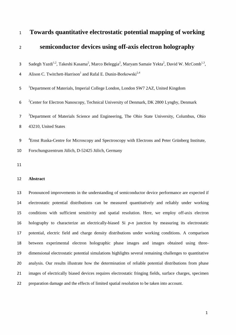
Figure 5. a) Representative 3D simulation of the electrostatic potential inside and around a 500-nm-
thick parallel-sided specimen containing an abrupt symmetrical Si p-n junction for an applied bias of
0 V. Only half of the simulated volume (cut at the xy plane) is shown, so that the potential variation
within and around the specimen can be seen. A corresponding phase image, limited to a volume of
27
x = 0.1 to x = 1.1 µm, y = 0.1 to y = 0.9 µm and z = -1 to 1 µm in (a), and its eight-times-amplified
phase contours calculated for an accelerating voltage of 120 kV at 0 V bias, are shown in b) and c).
The effect of the perturbed reference wave is taken into account in (c), but not in (b). The profiles in
(d) show the phase change across the junction at 0 V (a, b and c) and 2 V (aʹ, bʹ and cʹ) reverse bias.
The profiles marked (a) and (aʹ) show the phase change across the junction within the specimen
without considering the effects of fringing fields; those marked (b) and (bʹ) show the entire phase
change across the junction, including the effects of fringing fields above and below the specimen;
those marked (c) and (cʹ) include the effect of the perturbed reference wave. e) Contributions to the
measured phase step across the junction plotted as a function of applied reverse bias from the interior
of the specimen (black triangles), from the entire simulated volume without considering the perturbed
reference wave (blue circles) and from the entire simulated volume taking the perturbed reference
wave into account (red squares). f) and g) show electric field and charge density profiles for different
applied bias voltages determined from the contribution to the phase shift from fringing fields alone.
Similar to the experimental measurements shown in Fig. 1, all of the profiles are taken 300 nm away
from the sample edge.
525

28

29
Figure 6. a) Representative 3D simulation of the electrostatic potential inside and around a 500-nm-
thick parallel-sided specimen containing an abrupt symmetrical Si p-n junction, calculated for an
applied reverse bias of 0 V with a positive surface charge density of 8×10¹²
e.c./cm2 on all three
surfaces of the specimen (x = 0.5 µm, z = - 0.25 µm and z = 0.25 µm). b) Corresponding phase image
and its eight-times-amplified phase contours. c) Contributions to the phase step across the junction
measured only from the interior of the specimen (black triangles), from the entire simulated volume
(red squares) and only from the fringing fields above and below the specimen (green diamonds). d)
and e) show electric field and charge density profiles for different applied bias voltages determined
from the phase profiles corresponding solely to contributions from fringing fields. f) and g) show
electric field and charge density profiles for different applied bias voltages, determined from phase
profiles corresponding to the entire simulated potential volume. All profiles are taken 300 nm away
from the sample edge.
526