tpa6120a2rgy evaluation module - analog, … · the tpa6120a2rgy evm is designed to operate...
TRANSCRIPT

User's GuideSLOU394–July 2014
TPA6120A2RGY Evaluation Module
This user's guide describes the characteristics, operation, and use of the TPA6120A2RGY evaluationmodule (EVM). This user's guide includes EVM description, performance specifications, board layout, billof materials (BOM), and schematic diagram.
Contents1 Introduction ................................................................................................................... 2
1.1 Related Documentation from Texas Instruments............................................................... 21.2 Description........................................................................................................... 21.3 Performance Specifications ....................................................................................... 2
2 Getting Started ............................................................................................................... 23 Customizing the EVM ....................................................................................................... 4
3.1 Single-Ended Inverting Configuration ............................................................................ 43.2 Single-Ended Noninverting Configuration ....................................................................... 43.3 Special Note on Filtering and Capacitors C7 and C8 .......................................................... 43.4 Special Note on Gain and Input Configurations ................................................................ 43.5 Single Power Supply Configuration .............................................................................. 4
4 EVM Circuit and Layout..................................................................................................... 54.1 Layout Guidelines................................................................................................... 54.2 TPA6120A2RGY EVM PCB Layouts............................................................................. 54.3 Schematic............................................................................................................ 74.4 Bill of Materials ...................................................................................................... 7
List of Figures
1 TPA6120A2RGY EVM Top Layer ......................................................................................... 32 TPA6120A2RGY EVM Top Copper Layer................................................................................ 53 TPA6120A2RGY EVM Middle Layer 1 ................................................................................... 54 TPA6120A2RGY EVM Middle Layer 2.................................................................................... 55 TPA6120A2RGY EVM Bottom Layer ..................................................................................... 56 TPA6120A2RGY EVM Schematic......................................................................................... 7
List of Tables
1 TPA6120A2RGY EVM Specifications..................................................................................... 22 TPA6120A2RGY EVM Bill of Materials ................................................................................... 7
1SLOU394–July 2014 TPA6120A2RGY Evaluation ModuleSubmit Documentation Feedback
Copyright © 2014, Texas Instruments Incorporated
Introduction www.ti.com
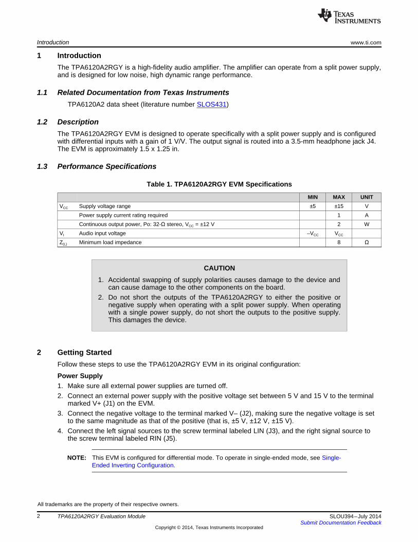
1 IntroductionThe TPA6120A2RGY is a high-fidelity audio amplifier. The amplifier can operate from a split power supply,and is designed for low noise, high dynamic range performance.
1.1 Related Documentation from Texas InstrumentsTPA6120A2 data sheet (literature number SLOS431)
1.2 DescriptionThe TPA6120A2RGY EVM is designed to operate specifically with a split power supply and is configuredwith differential inputs with a gain of 1 V/V. The output signal is routed into a 3.5-mm headphone jack J4.The EVM is approximately 1.5 x 1.25 in.
1.3 Performance Specifications
Table 1. TPA6120A2RGY EVM Specifications
MIN MAX UNITVCC Supply voltage range ±5 ±15 V
Power supply current rating required 1 AContinuous output power, Po: 32-Ω stereo, VCC = ±12 V 2 W
VI Audio input voltage –VCC VCC
Z(L) Minimum load impedance 8 Ω
CAUTION1. Accidental swapping of supply polarities causes damage to the device and
can cause damage to the other components on the board.2. Do not short the outputs of the TPA6120A2RGY to either the positive or
negative supply when operating with a split power supply. When operatingwith a single power supply, do not short the outputs to the positive supply.This damages the device.
2 Getting StartedFollow these steps to use the TPA6120A2RGY EVM in its original configuration:
Power Supply1. Make sure all external power supplies are turned off.2. Connect an external power supply with the positive voltage set between 5 V and 15 V to the terminal
marked V+ (J1) on the EVM.3. Connect the negative voltage to the terminal marked V– (J2), making sure the negative voltage is set
to the same magnitude as that of the positive (that is, ±5 V, ±12 V, ±15 V).4. Connect the left signal sources to the screw terminal labeled LIN (J3), and the right signal source to
the screw terminal labeled RIN (J5).
NOTE: This EVM is configured for differential mode. To operate in single-ended mode, see Single-Ended Inverting Configuration.
All trademarks are the property of their respective owners.
2 TPA6120A2RGY Evaluation Module SLOU394–July 2014Submit Documentation Feedback
Copyright © 2014, Texas Instruments Incorporated

www.ti.com Getting Started
Inputs and Outputs1. Ensure the signal source is turned off or set to a minimum.2. Connect the left signal source to the RCA jack labeled LIN+ (J5), and the right signal source to the
RCA jack labeled RIN+ (J6).3. Insert headphones into 3.5 mm headphone jack (J4).
Power Up1. Verify correct voltage polarity on the supplies.2. Turn on the power supply.3. Turn on the signal source.4. Adjust signal source level as needed.
Figure 1. TPA6120A2RGY EVM Top Layer
3SLOU394–July 2014 TPA6120A2RGY Evaluation ModuleSubmit Documentation Feedback
Copyright © 2014, Texas Instruments Incorporated

Customizing the EVM www.ti.com
3 Customizing the EVMThe TPA6120A2RGY EVM comes in a differential configuration with a gain of 1 V/V. However, the EVM isdesigned to be flexible, and can be converted to operate in single-ended inverting and noninvertingconfigurations. The TPA6120A2RGY EVM can also be operated in a single power supply configuration.
3.1 Single-Ended Inverting ConfigurationThe TPA6120A2RGY EVM can operate in a single-ended inverting gain configuration without modification.To operate in single-ended mode with the unmodified EVM, simply put the signal line into the invertingterminal (–) and the ground line into the noninverting terminal (+). This yields an inverting configurationwith a gain of –1 V/V.
The EVM can also be modified to operate in single-ended inverting only mode with a reduced BOM. To dothis, short resistors R1, R2, R9 (for the left channel) and short R10, R11, and R12 (for the right channel).Put the signal line on the inverting terminal and the ground line on the noninverting terminal. This yields aninverting configuration with a gain of –1 V/V.
3.2 Single-Ended Noninverting ConfigurationThe EVM can operate in a single-ended noninverting gain configuration without modification by applyingthe signal line to the noninverting input and the ground line to the inverting input. This yields a gain of +1V/V.
Another possible setup for noninverting configuration is to remove R9 (for the left channel) and R10 (forthe right channel). Apply the signal line to the noninverting input and the ground line to the inverting input.This yields a gain of +2 V/V.
3.3 Special Note on Filtering and Capacitors C7 and C8Capacitors C7 and C8 can be added into the EVM to form a low-pass filter into the amplifier. A typicalapplication for this is to block out the band noise caused by the output of a DAC. When selectingcapacitance values, the cut-off frequency of the filter becomes 1/(π × R × C) instead of 1/(2π × R × C)because the capacitor is connected differentially, which halves the required capacitance.
3.4 Special Note on Gain and Input ConfigurationsThe TPA6120A2RGY high-fidelity audio power amplifier has two separate channels, left and right. It is notnecessary to operate each channel in the same configuration. For test purposes, it may be desirable tooperate the left channel with a noninverting configuration, and the right channel with an invertingconfiguration. One channel may be configured to operate with differential inputs while the other channelwith single-ended inputs. The TPA6120A2RGY EVM allows for this flexibility. From a listening standpoint,the best audio performance is achieved when both channels are operated with the same configuration. Inthis case, there is no sound difference between the left and right channels for the human ear to detect.
3.5 Single Power Supply ConfigurationThe TPA6120A2RGY EVM was not optimized for single power supply operation. To operate in this mode,the V– terminal must be connected to GND. DC-blocking capacitors must be used at the outputs toprevent large amounts of dc current from flowing through the headphones due to the high midrail bias.Likewise, dc-blocking capacitors must be used at the input. R9 and R10 must be removed. The positiveinput nodes must be biased to midrail. Resistors R9 and R10 tie the positive node to ground.
4 TPA6120A2RGY Evaluation Module SLOU394–July 2014Submit Documentation Feedback
Copyright © 2014, Texas Instruments Incorporated

www.ti.com EVM Circuit and Layout
4 EVM Circuit and LayoutThe TPA6120A2RGY EVM layout was carefully planned to minimize the capacitance and inductancedetected by the output and input pins of the amplifier.
This chapter includes the EVM layout, the TPA6120A2RGY EVM component selection, schematic, andBOM.
4.1 Layout GuidelinesUse the following guidelines during layout:• Keep layout tight to minimize layout parasitics (that is, keep traces as short as possible and do not
cross signal lines, if possible)• Maintain symmetry in the layout to maximize common-mode rejection (CMR)• Maximize copper area connection to the PowerPad for best heat dissipation performance (if cutting the
ground plane, make cuts radially and not circularly)• Remove ground plane from inputs to minimize stray capacitance
4.2 TPA6120A2RGY EVM PCB LayoutsFigure 2 shows the top copper layer of the TPA6120A2RGY EVM. The RCA jacks at the inputs areconfigured to short to ground when no plug is inserted. The noninverting configuration of the EVM requiresthat RIN. and LIN. be at ground. Rather than have the signal go through the long signal trace to get to theinput jacks, 0-Ω resistors R11 and R12 are used to provide a connection to ground much closer to thedevice.
A star point for ground should be chosen. For the TPA6120A2RGY EVM, the ground terminal of the boardis (J7). Current paths to the star ground should be as direct as possible.
Figure 3 through Figure 5 illustrate other TPA6120A2RGY EVM copper layers.
Figure 2. TPA6120A2RGY EVM Top Copper Layer Figure 3. TPA6120A2RGY EVM Middle Layer 1
5SLOU394–July 2014 TPA6120A2RGY Evaluation ModuleSubmit Documentation Feedback
Copyright © 2014, Texas Instruments Incorporated

EVM Circuit and Layout www.ti.com
Figure 4. TPA6120A2RGY EVM Middle Layer 2 Figure 5. TPA6120A2RGY EVM Bottom Layer
6 TPA6120A2RGY Evaluation Module SLOU394–July 2014Submit Documentation Feedback
Copyright © 2014, Texas Instruments Incorporated

2
1
3
J4
SJ-3523-SMT
0.1µFC2
10µFC1
0.1µFC3
0.1µFC4
0.1µFC5
10µFC6
GND GND
GND GNDGND GND GND GND
1
2
J1
1
2
J3
1
2
J5
1000pFC8
DNP
DNP
1000pFC7
DNP
DNP
402
R1
402
R5
402
R7
402
R11
402
R2
402
R6
402
R8
402
R12GND
806R9
806R10
GND GND 806
R13
806
R14
39.2
R3
GND
39.2
R4
1
2
J2
LIN+1
LIN-2
NC3
NC4
NC5
RIN-6
RIN+7
RVCC+8
ROUT9
RVCC-10
NC11
LVCC-12
LOUT13
LVCC+14
PAD15
U1
TPA6120A2RGY
www.ti.com EVM Circuit and Layout
4.3 SchematicFigure 6 illustrates the TPA6120A2RGY EVM schematic.
Figure 6. TPA6120A2RGY EVM Schematic
4.4 Bill of MaterialsTable 2 list the BOM for this EVM.
Table 2. TPA6120A2RGY EVM Bill of Materials (1)
Designator Qty Value Description Package Part Number ManufacturerReference
!PCB 1 Printed Circuit Board AIP022 Any
C1 1 10uF CAP, CERM, 10uF, 25V, +/-20%, 0603 C1608X5R1E106M080AC TDK CorporationX5R, 0603
C2, C3, C4, 4 0.1uF CAP, CERM, 0.1uF, 25V, +/-10%, 0603 GRM188R71E104KA01D MuRataC5 X7R, 0603
C6 1 10uF CAP, CERM, 10uF, 25V, +/-20%, 0603 GRM188R61E106MA73 MuRataX5R, 0603
H1, H2, H3, 4 Bumpon, Hemisphere, 0.25 X 0.075, 75x250 mil SJ5382 3MH4 Clear
J1, J2, J3, J5 4 Terminal Block, 6A, 3.5mm Pitch, 2- 7.0x8.2x6.5mm ED555/2DS On-Shore TechnologyPos, TH
J4 1 Connector, Audio Jack, 3.5mm, Audio Jack SMD SJ-3523-SMT CUI Inc.Stereo, SMD
R1, R2, R5, 8 402 RES, 402 ohm, 1%, 0.1W, 0603 0603 RC0603FR-07402RL Yageo AmericaR6, R7, R8,R11, R12
R3, R4 2 39.2 RES, 39.2 ohm, 1%, 0.125W, 0805 0805 CRCW080539R2FKEA Vishay-Dale
R9, R10, 4 806 RES, 806 ohm, 1%, 0.1W, 0603 0603 CRCW0603806RFKEA Vishay-DaleR13, R14
U1 1 HIGH FIDELITY HEADPHONE RGY0014A TPA6120A2RGY Texas InstrumentsAMPLIFIER, RGY0014A
C7, C8 0 1000pF CAP, CERM, 1000pF, 25V, +/-5%, 0603 GRM1885C1E102JA01D MuRataC0G/NP0, 0603
FID1, FID2, 0 Fiducial mark. There is nothing to buy Fiducial N/A N/AFID3 or mount.
(1) Unless otherwise noted, all parts may be substituted with equivalents.
7SLOU394–July 2014 TPA6120A2RGY Evaluation ModuleSubmit Documentation Feedback
Copyright © 2014, Texas Instruments Incorporated

ADDITIONAL TERMS AND CONDITIONS, WARNINGS, RESTRICTIONS, AND DISCLAIMERS FOREVALUATION MODULES
Texas Instruments Incorporated (TI) markets, sells, and loans all evaluation boards, kits, and/or modules (EVMs) pursuant to, and userexpressly acknowledges, represents, and agrees, and takes sole responsibility and risk with respect to, the following:
1. User agrees and acknowledges that EVMs are intended to be handled and used for feasibility evaluation only in laboratory and/ordevelopment environments. Notwithstanding the foregoing, in certain instances, TI makes certain EVMs available to users that do nothandle and use EVMs solely for feasibility evaluation only in laboratory and/or development environments, but may use EVMs in ahobbyist environment. All EVMs made available to hobbyist users are FCC certified, as applicable. Hobbyist users acknowledge, agree,and shall comply with all applicable terms, conditions, warnings, and restrictions in this document and are subject to the disclaimer andindemnity provisions included in this document.
2. Unless otherwise indicated, EVMs are not finished products and not intended for consumer use. EVMs are intended solely for use bytechnically qualified electronics experts who are familiar with the dangers and application risks associated with handling electricalmechanical components, systems, and subsystems.
3. User agrees that EVMs shall not be used as, or incorporated into, all or any part of a finished product.4. User agrees and acknowledges that certain EVMs may not be designed or manufactured by TI.5. User must read the user's guide and all other documentation accompanying EVMs, including without limitation any warning or
restriction notices, prior to handling and/or using EVMs. Such notices contain important safety information related to, for example,temperatures and voltages. For additional information on TI's environmental and/or safety programs, please visit www.ti.com/esh orcontact TI.
6. User assumes all responsibility, obligation, and any corresponding liability for proper and safe handling and use of EVMs.7. Should any EVM not meet the specifications indicated in the user’s guide or other documentation accompanying such EVM, the EVM
may be returned to TI within 30 days from the date of delivery for a full refund. THE FOREGOING LIMITED WARRANTY IS THEEXCLUSIVE WARRANTY MADE BY TI TO USER AND IS IN LIEU OF ALL OTHER WARRANTIES, EXPRESSED, IMPLIED, ORSTATUTORY, INCLUDING ANY WARRANTY OF MERCHANTABILITY OR FITNESS FOR ANY PARTICULAR PURPOSE. TI SHALLNOT BE LIABLE TO USER FOR ANY INDIRECT, SPECIAL, INCIDENTAL, OR CONSEQUENTIAL DAMAGES RELATED TO THEHANDLING OR USE OF ANY EVM.
8. No license is granted under any patent right or other intellectual property right of TI covering or relating to any machine, process, orcombination in which EVMs might be or are used. TI currently deals with a variety of customers, and therefore TI’s arrangement withthe user is not exclusive. TI assumes no liability for applications assistance, customer product design, software performance, orinfringement of patents or services with respect to the handling or use of EVMs.
9. User assumes sole responsibility to determine whether EVMs may be subject to any applicable federal, state, or local laws andregulatory requirements (including but not limited to U.S. Food and Drug Administration regulations, if applicable) related to its handlingand use of EVMs and, if applicable, compliance in all respects with such laws and regulations.
10. User has sole responsibility to ensure the safety of any activities to be conducted by it and its employees, affiliates, contractors ordesignees, with respect to handling and using EVMs. Further, user is responsible to ensure that any interfaces (electronic and/ormechanical) between EVMs and any human body are designed with suitable isolation and means to safely limit accessible leakagecurrents to minimize the risk of electrical shock hazard.
11. User shall employ reasonable safeguards to ensure that user’s use of EVMs will not result in any property damage, injury or death,even if EVMs should fail to perform as described or expected.
12. User shall be solely responsible for proper disposal and recycling of EVMs consistent with all applicable federal, state, and localrequirements.
Certain Instructions. User shall operate EVMs within TI’s recommended specifications and environmental considerations per the user’sguide, accompanying documentation, and any other applicable requirements. Exceeding the specified ratings (including but not limited toinput and output voltage, current, power, and environmental ranges) for EVMs may cause property damage, personal injury or death. Ifthere are questions concerning these ratings, user should contact a TI field representative prior to connecting interface electronics includinginput power and intended loads. Any loads applied outside of the specified output range may result in unintended and/or inaccurateoperation and/or possible permanent damage to the EVM and/or interface electronics. Please consult the applicable EVM user's guide priorto connecting any load to the EVM output. If there is uncertainty as to the load specification, please contact a TI field representative. Duringnormal operation, some circuit components may have case temperatures greater than 60°C as long as the input and output are maintainedat a normal ambient operating temperature. These components include but are not limited to linear regulators, switching transistors, passtransistors, and current sense resistors which can be identified using EVMs’ schematics located in the applicable EVM user's guide. Whenplacing measurement probes near EVMs during normal operation, please be aware that EVMs may become very warm. As with allelectronic evaluation tools, only qualified personnel knowledgeable in electronic measurement and diagnostics normally found indevelopment environments should use EVMs.Agreement to Defend, Indemnify and Hold Harmless. User agrees to defend, indemnify, and hold TI, its directors, officers, employees,agents, representatives, affiliates, licensors and their representatives harmless from and against any and all claims, damages, losses,expenses, costs and liabilities (collectively, "Claims") arising out of, or in connection with, any handling and/or use of EVMs. User’sindemnity shall apply whether Claims arise under law of tort or contract or any other legal theory, and even if EVMs fail to perform asdescribed or expected.Safety-Critical or Life-Critical Applications. If user intends to use EVMs in evaluations of safety critical applications (such as life support),and a failure of a TI product considered for purchase by user for use in user’s product would reasonably be expected to cause severepersonal injury or death such as devices which are classified as FDA Class III or similar classification, then user must specifically notify TIof such intent and enter into a separate Assurance and Indemnity Agreement.

RADIO FREQUENCY REGULATORY COMPLIANCE INFORMATION FOR EVALUATION MODULESTexas Instruments Incorporated (TI) evaluation boards, kits, and/or modules (EVMs) and/or accompanying hardware that is marketed, sold,or loaned to users may or may not be subject to radio frequency regulations in specific countries.General Statement for EVMs Not Including a RadioFor EVMs not including a radio and not subject to the U.S. Federal Communications Commission (FCC) or Industry Canada (IC)regulations, TI intends EVMs to be used only for engineering development, demonstration, or evaluation purposes. EVMs are not finishedproducts typically fit for general consumer use. EVMs may nonetheless generate, use, or radiate radio frequency energy, but have not beentested for compliance with the limits of computing devices pursuant to part 15 of FCC or the ICES-003 rules. Operation of such EVMs maycause interference with radio communications, in which case the user at his own expense will be required to take whatever measures maybe required to correct this interference.General Statement for EVMs including a radioUser Power/Frequency Use Obligations: For EVMs including a radio, the radio included in such EVMs is intended for development and/orprofessional use only in legally allocated frequency and power limits. Any use of radio frequencies and/or power availability in such EVMsand their development application(s) must comply with local laws governing radio spectrum allocation and power limits for such EVMs. It isthe user’s sole responsibility to only operate this radio in legally acceptable frequency space and within legally mandated power limitations.Any exceptions to this are strictly prohibited and unauthorized by TI unless user has obtained appropriate experimental and/or developmentlicenses from local regulatory authorities, which is the sole responsibility of the user, including its acceptable authorization.
U.S. Federal Communications Commission Compliance
For EVMs Annotated as FCC – FEDERAL COMMUNICATIONS COMMISSION Part 15 Compliant
CautionThis device complies with part 15 of the FCC Rules. Operation is subject to the following two conditions: (1) This device may not causeharmful interference, and (2) this device must accept any interference received, including interference that may cause undesired operation.Changes or modifications could void the user's authority to operate the equipment.
FCC Interference Statement for Class A EVM devicesThis equipment has been tested and found to comply with the limits for a Class A digital device, pursuant to part 15 of the FCC Rules.These limits are designed to provide reasonable protection against harmful interference when the equipment is operated in a commercialenvironment. This equipment generates, uses, and can radiate radio frequency energy and, if not installed and used in accordance with theinstruction manual, may cause harmful interference to radio communications. Operation of this equipment in a residential area is likely tocause harmful interference in which case the user will be required to correct the interference at its own expense.
FCC Interference Statement for Class B EVM devicesThis equipment has been tested and found to comply with the limits for a Class B digital device, pursuant to part 15 of the FCC Rules.These limits are designed to provide reasonable protection against harmful interference in a residential installation. This equipmentgenerates, uses and can radiate radio frequency energy and, if not installed and used in accordance with the instructions, may causeharmful interference to radio communications. However, there is no guarantee that interference will not occur in a particular installation. Ifthis equipment does cause harmful interference to radio or television reception, which can be determined by turning the equipment off andon, the user is encouraged to try to correct the interference by one or more of the following measures:
• Reorient or relocate the receiving antenna.• Increase the separation between the equipment and receiver.• Connect the equipment into an outlet on a circuit different from that to which the receiver is connected.• Consult the dealer or an experienced radio/TV technician for help.
Industry Canada Compliance (English)For EVMs Annotated as IC – INDUSTRY CANADA Compliant:
This Class A or B digital apparatus complies with Canadian ICES-003.Changes or modifications not expressly approved by the party responsible for compliance could void the user’s authority to operate theequipment.
Concerning EVMs Including Radio TransmittersThis device complies with Industry Canada licence-exempt RSS standard(s). Operation is subject to the following two conditions: (1) thisdevice may not cause interference, and (2) this device must accept any interference, including interference that may cause undesiredoperation of the device.
Concerning EVMs Including Detachable AntennasUnder Industry Canada regulations, this radio transmitter may only operate using an antenna of a type and maximum (or lesser) gainapproved for the transmitter by Industry Canada. To reduce potential radio interference to other users, the antenna type and its gain shouldbe so chosen that the equivalent isotropically radiated power (e.i.r.p.) is not more than that necessary for successful communication.This radio transmitter has been approved by Industry Canada to operate with the antenna types listed in the user guide with the maximumpermissible gain and required antenna impedance for each antenna type indicated. Antenna types not included in this list, having a gaingreater than the maximum gain indicated for that type, are strictly prohibited for use with this device.

Canada Industry Canada Compliance (French)
Cet appareil numérique de la classe A ou B est conforme à la norme NMB-003 du Canada
Les changements ou les modifications pas expressément approuvés par la partie responsable de la conformité ont pu vider l’autorité del'utilisateur pour actionner l'équipement.
Concernant les EVMs avec appareils radio
Le présent appareil est conforme aux CNR d'Industrie Canada applicables aux appareils radio exempts de licence. L'exploitation estautorisée aux deux conditions suivantes : (1) l'appareil ne doit pas produire de brouillage, et (2) l'utilisateur de l'appareil doit accepter toutbrouillage radioélectrique subi, même si le brouillage est susceptible d'en compromettre le fonctionnement.
Concernant les EVMs avec antennes détachables
Conformément à la réglementation d'Industrie Canada, le présent émetteur radio peut fonctionner avec une antenne d'un type et d'un gainmaximal (ou inférieur) approuvé pour l'émetteur par Industrie Canada. Dans le but de réduire les risques de brouillage radioélectrique àl'intention des autres utilisateurs, il faut choisir le type d'antenne et son gain de sorte que la puissance isotrope rayonnée équivalente(p.i.r.e.) ne dépasse pas l'intensité nécessaire à l'établissement d'une communication satisfaisante.
Le présent émetteur radio a été approuvé par Industrie Canada pour fonctionner avec les types d'antenne énumérés dans le manueld’usage et ayant un gain admissible maximal et l'impédance requise pour chaque type d'antenne. Les types d'antenne non inclus danscette liste, ou dont le gain est supérieur au gain maximal indiqué, sont strictement interdits pour l'exploitation de l'émetteur.
Mailing Address: Texas Instruments, Post Office Box 655303, Dallas, Texas 75265Copyright © 2014, Texas Instruments Incorporated
spacer
Important Notice for Users of EVMs Considered “Radio Frequency Products” in JapanEVMs entering Japan are NOT certified by TI as conforming to Technical Regulations of Radio Law of Japan.
If user uses EVMs in Japan, user is required by Radio Law of Japan to follow the instructions below with respect to EVMs:1. Use EVMs in a shielded room or any other test facility as defined in the notification #173 issued by Ministry of Internal Affairs and
Communications on March 28, 2006, based on Sub-section 1.1 of Article 6 of the Ministry’s Rule for Enforcement of Radio Law ofJapan,
2. Use EVMs only after user obtains the license of Test Radio Station as provided in Radio Law of Japan with respect to EVMs, or3. Use of EVMs only after user obtains the Technical Regulations Conformity Certification as provided in Radio Law of Japan with respect
to EVMs. Also, do not transfer EVMs, unless user gives the same notice above to the transferee. Please note that if user does notfollow the instructions above, user will be subject to penalties of Radio Law of Japan.
http://www.tij.co.jp
【無線電波を送信する製品の開発キットをお使いになる際の注意事項】 本開発キットは技術基準適合証明を受けておりません。 本製品のご使用に際しては、電波法遵守のため、以下のいずれかの措置を取っていただく必要がありますのでご注意ください。
1. 電波法施行規則第6条第1項第1号に基づく平成18年3月28日総務省告示第173号で定められた電波暗室等の試験設備でご使用いただく。2. 実験局の免許を取得後ご使用いただく。3. 技術基準適合証明を取得後ご使用いただく。。
なお、本製品は、上記の「ご使用にあたっての注意」を譲渡先、移転先に通知しない限り、譲渡、移転できないものとします
上記を遵守頂けない場合は、電波法の罰則が適用される可能性があることをご留意ください。
日本テキサス・インスツルメンツ株式会社東京都新宿区西新宿6丁目24番1号西新宿三井ビルhttp://www.tij.co.jp
Texas Instruments Japan Limited(address) 24-1, Nishi-Shinjuku 6 chome, Shinjuku-ku, Tokyo, Japan

IMPORTANT NOTICETexas Instruments Incorporated and its subsidiaries (TI) reserve the right to make corrections, enhancements, improvements and otherchanges to its semiconductor products and services per JESD46, latest issue, and to discontinue any product or service per JESD48, latestissue. Buyers should obtain the latest relevant information before placing orders and should verify that such information is current andcomplete. All semiconductor products (also referred to herein as “components”) are sold subject to TI’s terms and conditions of salesupplied at the time of order acknowledgment.TI warrants performance of its components to the specifications applicable at the time of sale, in accordance with the warranty in TI’s termsand conditions of sale of semiconductor products. Testing and other quality control techniques are used to the extent TI deems necessaryto support this warranty. Except where mandated by applicable law, testing of all parameters of each component is not necessarilyperformed.TI assumes no liability for applications assistance or the design of Buyers’ products. Buyers are responsible for their products andapplications using TI components. To minimize the risks associated with Buyers’ products and applications, Buyers should provideadequate design and operating safeguards.TI does not warrant or represent that any license, either express or implied, is granted under any patent right, copyright, mask work right, orother intellectual property right relating to any combination, machine, or process in which TI components or services are used. Informationpublished by TI regarding third-party products or services does not constitute a license to use such products or services or a warranty orendorsement thereof. Use of such information may require a license from a third party under the patents or other intellectual property of thethird party, or a license from TI under the patents or other intellectual property of TI.Reproduction of significant portions of TI information in TI data books or data sheets is permissible only if reproduction is without alterationand is accompanied by all associated warranties, conditions, limitations, and notices. TI is not responsible or liable for such altereddocumentation. Information of third parties may be subject to additional restrictions.Resale of TI components or services with statements different from or beyond the parameters stated by TI for that component or servicevoids all express and any implied warranties for the associated TI component or service and is an unfair and deceptive business practice.TI is not responsible or liable for any such statements.Buyer acknowledges and agrees that it is solely responsible for compliance with all legal, regulatory and safety-related requirementsconcerning its products, and any use of TI components in its applications, notwithstanding any applications-related information or supportthat may be provided by TI. Buyer represents and agrees that it has all the necessary expertise to create and implement safeguards whichanticipate dangerous consequences of failures, monitor failures and their consequences, lessen the likelihood of failures that might causeharm and take appropriate remedial actions. Buyer will fully indemnify TI and its representatives against any damages arising out of the useof any TI components in safety-critical applications.In some cases, TI components may be promoted specifically to facilitate safety-related applications. With such components, TI’s goal is tohelp enable customers to design and create their own end-product solutions that meet applicable functional safety standards andrequirements. Nonetheless, such components are subject to these terms.No TI components are authorized for use in FDA Class III (or similar life-critical medical equipment) unless authorized officers of the partieshave executed a special agreement specifically governing such use.Only those TI components which TI has specifically designated as military grade or “enhanced plastic” are designed and intended for use inmilitary/aerospace applications or environments. Buyer acknowledges and agrees that any military or aerospace use of TI componentswhich have not been so designated is solely at the Buyer's risk, and that Buyer is solely responsible for compliance with all legal andregulatory requirements in connection with such use.TI has specifically designated certain components as meeting ISO/TS16949 requirements, mainly for automotive use. In any case of use ofnon-designated products, TI will not be responsible for any failure to meet ISO/TS16949.Products ApplicationsAudio www.ti.com/audio Automotive and Transportation www.ti.com/automotiveAmplifiers amplifier.ti.com Communications and Telecom www.ti.com/communicationsData Converters dataconverter.ti.com Computers and Peripherals www.ti.com/computersDLP® Products www.dlp.com Consumer Electronics www.ti.com/consumer-appsDSP dsp.ti.com Energy and Lighting www.ti.com/energyClocks and Timers www.ti.com/clocks Industrial www.ti.com/industrialInterface interface.ti.com Medical www.ti.com/medicalLogic logic.ti.com Security www.ti.com/securityPower Mgmt power.ti.com Space, Avionics and Defense www.ti.com/space-avionics-defenseMicrocontrollers microcontroller.ti.com Video and Imaging www.ti.com/videoRFID www.ti-rfid.comOMAP Applications Processors www.ti.com/omap TI E2E Community e2e.ti.comWireless Connectivity www.ti.com/wirelessconnectivity
Mailing Address: Texas Instruments, Post Office Box 655303, Dallas, Texas 75265Copyright © 2014, Texas Instruments Incorporated