tps389x single-channel, adjustable voltage monitor in ... · tps389 sbvs172b –july 2011–revised...
TRANSCRIPT

493
495
497
499
501
503
505
507
−40 −25 −10 5 20 35 50 65 80 95 110 125Temperature (°C)
VIT
+, V
IT+ −
VH
YS (
mV
)
VCC = 1.7 V, VIT+VCC = 3.3 V, VIT+VCC = 6.5 V, VIT+VCC = 1.7 V, VIT+ − VHYSVCC = 3.3 V, VIT+ − VHYSVCC = 6.5 V, VIT+ − VHYS
G004
Product
Folder
Sample &Buy
Technical
Documents
Tools &
Software
Support &Community
TPS389SBVS172B –JULY 2011–REVISED APRIL 2015
TPS389x Single-Channel, Adjustable Voltage Monitor in Ultra-Small Package1 Features 3 Description
The TPS3895, TPS3896, TPS3897, and TPS38981• Very Small USON (1.45 mm × 1.00 mm) Package
devices (TPS389x) are a family of very small• Adjustable Threshold Down to 500 mV supervisory circuits that monitor voltages greater than• Threshold Accuracy: 1% Over Temperature 500 mV with a 0.25% (typical) threshold accuracy
and offer adjustable delay time using external• Capacitor-Adjustable Delay Timecapacitors. The TPS389x family also has a logic• Low Quiescent Current: 6 µA (Typical) enable pin (ENABLE or ENABLE) to power on and off
• External Enable Input the output. With the TPS3895, for example, when theinput voltage pin (SENSE) rises above the threshold,• Open-Drain (Rated at 18 V) and Push-Pull Outputand the ENABLE pin is high, then the output pinOptions(SENSE_OUT) goes high after the capacitor-• Temperature Range: –40°C to 125°C adjustable delay time. When SENSE falls below the
• Pin-for-Pin Compatible With MAX6895/6/7/8 threshold or ENABLE is low, then SENSE_OUT goeslow. For truth tables, see Table 1 and Table 2.
2 ApplicationsFor TPS389xA versions, both SENSE and ENABLE
• DSPs, Microcontrollers, and Microprocessors have a capacitor-adjustable delay. The output assertsafter this capacitor-adjustable delay when both• Notebook and Desktop ComputersSENSE and ENABLE inputs are good. The• PDAs and Handheld ProductsTPS389xP devices have a small, 0.2-µs propagation
• Portable and Battery-Powered Products delay from when the enable pin asserts to when the• FPGAs and ASICs output pin asserts, provided SENSE is above the
threshold.
All devices operate from 1.7 V to 6.5 V and have atypical quiescent current of 6 µA with an open-drainoutput rated at 18 V. The TPS389x is available in anultra-small USON package and is fully specified overthe temperature range of TJ = –40°C to 125°C.
Device Information(1)
PART NUMBER PACKAGE BODY SIZE (NOM)TPS389x USON (6) 1.45 mm × 1.00 mm
(1) For all available packages, see the orderable addendum atthe end of the data sheet.
Sense Threshold Voltage vs Temperature
1
An IMPORTANT NOTICE at the end of this data sheet addresses availability, warranty, changes, use in safety-critical applications,intellectual property matters and other important disclaimers. PRODUCTION DATA.

TPS389SBVS172B –JULY 2011–REVISED APRIL 2015 www.ti.com
Table of Contents8.3 Feature Description................................................. 141 Features .................................................................. 18.4 Device Functional Modes........................................ 152 Applications ........................................................... 1
9 Applications and Implementation ...................... 163 Description ............................................................. 19.1 Application Information............................................ 164 Revision History..................................................... 29.2 Typical Applications ................................................ 165 Device Comparison Table ..................................... 3
10 Power Supply Recommendations ..................... 236 Pin Configuration and Functions ......................... 411 Layout................................................................... 237 Specifications......................................................... 5
11.1 Layout Guidelines ................................................. 237.1 Absolute Maximum Ratings ...................................... 511.2 Layout Example .................................................... 237.2 ESD Ratings ............................................................ 5
12 Device and Documentation Support ................. 247.3 Recommended Operating Conditions....................... 512.1 Device Support...................................................... 247.4 Thermal Information .................................................. 512.2 Documentation Support ........................................ 247.5 Electrical Characteristics........................................... 612.3 Trademarks ........................................................... 247.6 Timing Requirements ................................................ 712.4 Electrostatic Discharge Caution............................ 247.7 Typical Characteristics .............................................. 912.5 Glossary ................................................................ 248 Detailed Description ............................................ 12
13 Mechanical, Packaging, and Orderable8.1 Overview ................................................................. 12Information ........................................................... 248.2 Functional Block Diagram ....................................... 12
4 Revision History
Changes from Revision A (September 2011) to Revision B Page
• Added ESD Ratings table, Feature Description section, Device Functional Modes, Application and Implementationsection, Power Supply Recommendations section, Layout section, Device and Documentation Support section, andMechanical, Packaging, and Orderable Information section ................................................................................................. 1
• Changed paragraph 1 of Description section; revised for clarification .................................................................................. 1• Changed Pin Configuration and Functions section; updated table format, renamed pin packages to meet new
standards ............................................................................................................................................................................... 4
2 Submit Documentation Feedback Copyright © 2011–2015, Texas Instruments Incorporated
Product Folder Links: TPS389

TPS389www.ti.com SBVS172B –JULY 2011–REVISED APRIL 2015
5 Device Comparison Table
DEVICE ENABLE OUTPUT INPUT (SENSE) DELAY ENABLE DELAY
TPS3895A Active high Active high, push-pull Capacitor adjustable Capacitor adjustable
TPS3895P Active high Active high, push-pull Capacitor adjustable 0.2 µs
TPS3896A Active low Active low, push-pull Capacitor adjustable Capacitor adjustable
TPS3896P Active low Active low, push-pull Capacitor adjustable 0.2 µs
TPS3897A Active high Active high, open drain Capacitor adjustable Capacitor adjustable
TPS3897P Active high Active high, open drain Capacitor adjustable 0.2 µs
TPS3898A Active low Active low, open drain Capacitor adjustable Capacitor adjustable
TPS3898P Active low Active low, open drain Capacitor adjustable 0.2 µs
Copyright © 2011–2015, Texas Instruments Incorporated Submit Documentation Feedback 3
Product Folder Links: TPS389

ENABLE
GND
SENSE
VCC
CT
SENSE_OUT
1
2
3
6
5
4
ENABLE
GND
SENSE
VCC
CT
SENSE_OUT
1
2
3
6
5
4
TPS389SBVS172B –JULY 2011–REVISED APRIL 2015 www.ti.com
6 Pin Configuration and Functions
DRY Package: TPS3895, TPS38976-Pin USON
Top View
DRY Package: TPS3896, TPS38986-Pin USON
Top View
Pin FunctionsPIN
USON I/O DESCRIPTIONNAME TPS3895/ TPS3896/
TPS3897 TPS3898Capacitor-adjustable delay. The CT pin offers a user-adjustable delay time. Connectingthis pin to a ground referenced capacitor sets the delay time for SENSE rising above
CT 5 5 I 0.5 V to SENSE_OUT asserting (or ENABLE asserting to SENSE_OUT asserting for Aversion devices).tpd(r) (s) = [CCT (µF) × 4] + 40 µsActive high input. Driving ENABLE low immediately makes SENSE_OUT go low,independent of V(SENSE). With V(SENSE) already above VIT+, drive ENABLE high toENABLE 1 — I make SENSE_OUT go high after the capacitor-adjustable delay time (A version) or 0.2µs (P version).Active low input. Driving ENABLE high immediately makes SENSE_OUT go high,independent of V(SENSE). With V(SENSE) already above VIT+, drive ENABLE low to makeENABLE — 1 I SENSE_OUT go low after the capacitor-adjustable delay time (A version) or 0.2 µs (Pversion).
GND 2 2 — GroundThis pin is connected to the voltage that is monitored with the use of an externalresistor. The output asserts after the capacitor-adjustable delay time when V(SENSE)SENSE 3 3 I rises above 0.5 V and ENABLE is asserted. The output deasserts after a minimalpropagation delay (16 µs) when V(SENSE) falls below VIT+ – Vhys.SENSE_OUT is an open-drain and push-pull output that is immediately driven low afterV(SENSE) falls below (VIT+ – Vhys) or the ENABLE input is low. SENSE_OUT goes high
SENSE_OUT 4 — O after the capacitor-adjustable delay time when V(SENSE) is greater than VIT+ and theENABLE pin is high. Open-drain devices (TPS3897/8) can be pulled up to 18 Vindependent of VCC; pullup resistors are required for these devices.SENSE_OUT is an open-drain and push-pull output that is immediately driven highafter V(SENSE) falls below (VIT+ – Vhys) or the ENABLE input is high. SENSE_OUT goes
SENSE_OUT — 4 O low after the capacitor-adjustable delay time when V(SENSE) is greater than VIT+ and theENABLE pin is low. Open-drain devices (TPS3897/8) can be pulled up to 18 Vindependent of VCC; pullup resistors are required for these devices.Supply voltage input. Connect a 1.7-V to 6.5-V supply to VCC to power the device. It isVCC 6 6 I good analog design practice to place a 0.1-µF ceramic capacitor close to this pin.
4 Submit Documentation Feedback Copyright © 2011–2015, Texas Instruments Incorporated
Product Folder Links: TPS389

TPS389www.ti.com SBVS172B –JULY 2011–REVISED APRIL 2015
7 Specifications
7.1 Absolute Maximum RatingsOver operating free-air temperature range (unless otherwise noted). (1)
MIN MAX UNITVCC –0.3 7CT –0.3 VCC + 0.3
Voltage (2) ENABLE, SENSE, SENSE_OUT (push-pull) –0.3 7 VSENSE_OUT (open drain) –0.3 20SENSE_OUT (push-pull) –0.3 7
Current SENSE_OUT ±10 mAOperating junction, TJ –40 125
Temperature °CStorage, Tstg –65 150
(1) Stresses beyond those listed under Absolute Maximum Ratings may cause permanent damage to the device. These are stress ratingsonly, and functional operation of the device at these or any other conditions beyond those indicated under Recommended OperatingConditions is not implied. Exposure to absolute-maximum-rated conditions for extended periods my affect device reliability.
(2) All voltages are with respect to network ground terminal.
7.2 ESD RatingsVALUE UNIT
Human body model (HBM), per ANSI/ESDA/JEDEC JS-001, all pins (1) ±2000V(ESD) Electrostatic discharge VCharged device model (CDM), per JEDEC specification JESD22-C101, ±500all pins (2)
(1) JEDEC document JEP155 states that 500-V HBM allows safe manufacturing with a standard ESD control process.(2) JEDEC document JEP157 states that 250-V CDM allows safe manufacturing with a standard ESD control process.
7.3 Recommended Operating Conditionsover operating free-air temperature range (unless otherwise noted)
MIN NOM MAX UNITVCC Input supply voltage 1.7 6.5 VVENABLE, VENABLE ENABLE and ENABLE pin voltage 0 6.5 VVSENSE SENSE pin voltage 0 6.5 VVSENSE_OUT, VSENSE_OUT (open SENSE_OUT, SENSE_OUT pin voltage 0 18 Vdrain)
VSENSE_OUT, VSENSE_OUT SENSE_OUT, SENSE_OUT pin voltage 0 VCC V(push-pull)
ISENSE_OUT, ISENSE_OUT SENSE_OUT, SENSE_OUT pin current 0.0003 1 mA
7.4 Thermal InformationTPS389x
THERMAL METRIC (1) DRY (USON) UNIT6 PINS
RθJA Junction-to-ambient thermal resistance 293.8RθJC(top) Junction-to-case (top) thermal resistance 165.1RθJB Junction-to-board thermal resistance 160.8
°C/WψJT Junction-to-top characterization parameter 27.3ψJB Junction-to-board characterization parameter 65.8RθJC(bot) Junction-to-case (bottom) thermal resistance 65.8
(1) For more information about traditional and new thermal metrics, see the IC Package Thermal Metrics application report, SPRA953.
Copyright © 2011–2015, Texas Instruments Incorporated Submit Documentation Feedback 5
Product Folder Links: TPS389

TPS389SBVS172B –JULY 2011–REVISED APRIL 2015 www.ti.com
7.5 Electrical CharacteristicsOver the operating temperature range of TJ = –40°C to 125°C, and 1.7 V < VCC< 6.5 V, unless otherwise noted. Typicalvalues are at TJ = 25°C and VCC = 3.3 V.
PARAMETER TEST CONDITIONS MIN TYP MAX UNITTJ = –40°C to 125°C 1.7 6.5
VCC Supply voltage range VTJ = 0°C to 85°C 1.65 6.5
V(POR) Power-on reset voltage (1) VOL (max) = 0.2 V , I(SENSE_OUT) = 15 µA 0.8 VVCC = 3.3 V , no load 6 12
ICC Supply current (into VCC pin) µAVCC = 6.5 V , no load 7 12
VIT+ Positive-going input threshold voltage V(SENSE) rising 0.495 0.5 0.505 VVhys Hysteresis voltage V(SENSE) falling 5 mVI(SENSE) Input current (2) V(SENSE) = 0 V or VCC –15 15 nAI(CT) CT pin charge current 260 310 360 nAV(CT) CT pin comparator threshold voltage 1.18 1.238 1.299 VR(CT) CT pin pulldown resistance 200 ΩVIL Low-level input voltage (ENABLE pin) 0.4 VVIH High-level input voltage (ENABLE pin) 1.4 VUVLO Undervoltage lockout (3) VCC falling 1.3 1.7 VIlkg Leakage current ENABLE = VCC or GND –100 100 nA
VCC ≥ 1.2 V, ISINK = 90 µA (TPS3895/7 only) 0.3VOL Low-level output voltage VCC ≥ 2.25 V, ISINK = 0.5 mA 0.3 V
VCC ≥ 4.5 V, ISINK = 1 mA 0.4VCC ≥ 2.25 V, ISOURCE = 0.5 mA 0.8VCCVOH High-level output voltage (push-pull) VVCC ≥ 4.5 V, ISOURCE = 1 mA 0.8VCC
Ilkg(OD) Open-drain output leakage current V(SENSE_OUT) high impedance = 18 V 300 nA
(1) The lowest supply voltage (VCC) at which output is active (SENSE_OUT is low, SENSE_OUT is high); tr(VCC) > 15 µs/V. Below V(POR),the output cannot be determined.
(2) Specified by design.(3) When VCC falls below the UVLO threshold, the output deasserts (SENSE_OUT goes low, SENSE_OUT goes high). Below V(POR), the
output cannot be determined.
6 Submit Documentation Feedback Copyright © 2011–2015, Texas Instruments Incorporated
Product Folder Links: TPS389

V V-IT+ hys
VIT+
tpd(r)tpd(r)
VCC
SENSE
ENABLE
td(A)
V(POR)
tpd(f) td(OFF)
UVLO
SENSE_OUT
VIT+
TPS389www.ti.com SBVS172B –JULY 2011–REVISED APRIL 2015
7.6 Timing RequirementsMIN TYP MAX UNIT
V(SENSE) rising, C(CT) = 40 µsopentpd(r) SENSE (rising) to SENSE_OUT propagation delay
V(SENSE) rising, C(CT) = 190 ms0.047 µFtpd(f) SENSE (falling) to SENSE_OUT propagation delay V(SENSE) falling 16 µs
Start-up delay (1) 50 µstw ENABLE pin minimum pulse duration 1 µs
ENABLE pin glitch rejection 100 nsENABLE to SENSE_OUT delay time (output ENABLE deasserted totd(OFF) 200 nsdisabled) output deasserted
ENABLE asserted to outputtd(P) ENABLE to SENSE_OUT delay time (P version) asserted delay 200 ns
(P version)ENABLE asserted to outputasserted delay 20 µs(A version), C(CT) = open
td(A) ENABLE to SENSE_OUT delay time (A version) ENABLE asserted to outputasserted delay 190 ms(A version), C(CT) = 0.047µF
(1) During power on, VCC must exceed 1.7 V for at least 50 µs (plus propagation delay time, tpd(r)) before output is in the correct state.
Figure 1. TPS3895A and TPS3897A Timing
Copyright © 2011–2015, Texas Instruments Incorporated Submit Documentation Feedback 7
Product Folder Links: TPS389

V(POR)UVLO
tpd(r) td(OFF)tpd(f)
VIT+ VIT+
tpd(r) td(P)
V V-IT+ hys
VCC
SENSE
ENABLE
SENSE_OUT
VCC
SENSE
ENABLE
SENSE_OUT
V(POR)
VIT+ VIT+
V V-IT+ hys
tpd(r)tpd(r) td(A)tpd(f) td(OFF)
V V-IT+ hys
VIT+
tpd(r)tpd(r)
VCC
SENSE
ENABLE
td(P)
V(POR)
tpd(f) td(OFF)
SENSE_OUT
VIT+
TPS389SBVS172B –JULY 2011–REVISED APRIL 2015 www.ti.com
Figure 2. TPS3895P and TPS3897P Timing
Figure 3. TPS3896A and TPS3898A Timing
Figure 4. TPS3896P and TPS3898P Timing
8 Submit Documentation Feedback Copyright © 2011–2015, Texas Instruments Incorporated
Product Folder Links: TPS389

1
10
100
350
1 10 100Overdrive (%)
SE
NS
E P
ulse
Dur
atio
n (µ
s)
G005
0
50
100
150
200
250
300
350
400
450
0.1 0.2 0.3 0.4 0.5 0.6 0.7 0.8 0.9 1
VCC = 1.7 V
VCC = 3.3 V
VCC = 6.5 V
Output Sink Current (mA)
VO
L (m
V)
G006
186
187
188
189
190
191
192
193
194
195
196
−40 −25 −10 5 20 35 50 65 80 95 110 125
VCC = 1.7 V
VCC = 3.3 V
VCC = 6.5 V
Temperature (°C)
SE
NS
E_O
UT
Del
ay (
ms)
G003
493
495
497
499
501
503
505
507
−40 −25 −10 5 20 35 50 65 80 95 110 125Temperature (°C)
VIT
+, V
IT+ −
VH
YS (
mV
)
VCC = 1.7 V, VIT+VCC = 3.3 V, VIT+VCC = 6.5 V, VIT+VCC = 1.7 V, VIT+ − VHYSVCC = 3.3 V, VIT+ − VHYSVCC = 6.5 V, VIT+ − VHYS
G004
0
1
2
3
4
5
6
7
8
9
10
0 1 2 3 4 5 6 7VCC (V)
I CC (
µA)
−40°C0°C25°C85°C105°C125°C
G001
0
2
4
6
8
10
12
0 0.5 1 1.5 2 2.5 3CCT (µF)
SE
NS
E_O
UT
Del
ay (
s)
G002
TPS389www.ti.com SBVS172B –JULY 2011–REVISED APRIL 2015
7.7 Typical CharacteristicsAt TA = 25°C, and VCC = 3.3 V, unless otherwise noted.
Figure 5. Supply Current vs Supply Voltage Figure 6. SENSE_OUT Time-Out Period vs CCT
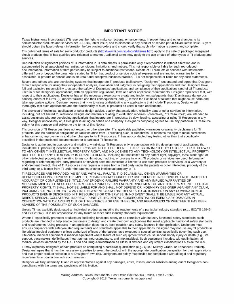
Figure 7. SENSE_OUT Time-Out Period vs Temperature Figure 8. SENSE Threshold Voltage vs Temperature(CCT = 47 nF)
Figure 9. SENSE Minimum Pulse Duration vs SENSE Figure 10. Output Voltage Low vs Output Current (0 mA toThreshold Overdrive Voltage 1 mA)
Copyright © 2011–2015, Texas Instruments Incorporated Submit Documentation Feedback 9
Product Folder Links: TPS389

0
1
2
3
4
5
6
7
0.5 1 1.5 2 2.5 3 3.5 4 4.5 5 5.5 6
VCC = 1.7 V
VCC = 3.3 V
VCC = 6.5 V
Output Source Current (mA)
VO
H (
V)
G011
Time (50 s/div)m
V
2V/divENABLE
V
2V/divSENSE_OUT
C = openCT
0
100
200
300
400
500
600
−40 −25 −10 5 20 35 50 65 80 95 110 125
VCC = 1.7 V
VCC = 3.3 V VCC = 6.5 V
Temperature (°C)
VC
C −
VO
H (
mV
)
G009
0
0.2
0.4
0.6
0.8
1
1.2
1.4
1.6
0.5 1 1.5 2 2.5 3 3.5 4 4.5 5 5.5 6
VCC = 1.7 V
VCC = 3.3 V
VCC = 6.5 V
Output Sink Current (mA)
VO
L (V
)
G010
0
50
100
150
200
250
300
350
400
450
0.1 0.2 0.3 0.4 0.5 0.6 0.7 0.8 0.9 1
VCC = 1.7 V
VCC = 3.3 V VCC = 6.5 V
Output Source Current (mA)
VC
C −
VO
H (
mV
)
G007
100
200
300
400
500
600
−40 −25 −10 5 20 35 50 65 80 95 110 125
VCC = 1.7 V
VCC = 3.3 V
VCC = 6.5 V
Temperature (°C)
VO
L (m
V)
G008
TPS389SBVS172B –JULY 2011–REVISED APRIL 2015 www.ti.com
Typical Characteristics (continued)At TA = 25°C, and VCC = 3.3 V, unless otherwise noted.
Figure 11. Output Voltage High vs Output Current Figure 12. Output Voltage Low at 1 mA vs Temperature(0 mA to 1 mA)
Figure 13. Output Voltage High at 1 mA vs Temperature Figure 14. Output Voltage Low vs Output Current
Figure 15. Output Voltage High vs Output Current Figure 16. Enable Power On and Power Off Delay(TPS3895A)
10 Submit Documentation Feedback Copyright © 2011–2015, Texas Instruments Incorporated
Product Folder Links: TPS389

Time (200ns/div)
V
2V/divENABLE
V
2V/divSENSE_OUT
TPS389www.ti.com SBVS172B –JULY 2011–REVISED APRIL 2015
Typical Characteristics (continued)At TA = 25°C, and VCC = 3.3 V, unless otherwise noted.
Figure 17. Enable Power On and Power Off Delay (TPS3895P)
Copyright © 2011–2015, Texas Instruments Incorporated Submit Documentation Feedback 11
Product Folder Links: TPS389

Delay
500 mV
VCC
SENSE
CT
GND
ENABLE
SENSE_OUT
TPS389SBVS172B –JULY 2011–REVISED APRIL 2015 www.ti.com
8 Detailed Description
8.1 OverviewThe TPS3895, TPS3896, TPS3897, and TPS3898 devices (TPS389x) are a family of ultra-small supervisorycircuits. The TPS389x is designed to assert the SENSE_OUT or SENSE_OUT signal, as shown in Table 1 andTable 2. When the SENSE pin rises above 0.5 V and the enable input is asserted (ENABLE = high or ENABLE =low) , the output asserts (SENSE_OUT goes high or SENSE_OUT goes low) after the capacitor-adjustable delaytime. The SENSE pin can be set to any voltage threshold above 0.5 V using an external resistor divider. A broadrange of output delay times and voltage thresholds can be supported, allowing these devices to be used in widearray of applications.
Table 1. TPS3895/7 Truth TableCONDITIONS OUTPUT STATUS
ENABLE = high SENSE < VIT+ SENSE_OUT = low Output not assertedENABLE = low SENSE < VIT+ SENSE_OUT = low Output not assertedENABLE = low SENSE > VIT+ SENSE_OUT = low Output not assertedENABLE = high SENSE > VIT+ SENSE_OUT = high Output asserted after delay
Table 2. TPS3896/8 Truth TableCONDITIONS OUTPUT STATUS
ENABLE = low SENSE < VIT+ SENSE_OUT = high Output not assertedENABLE = high SENSE < VIT+ SENSE_OUT = high Output not assertedENABLE = high SENSE > VIT+ SENSE_OUT = high Output not assertedENABLE = low SENSE > VIT+ SENSE_OUT = low Output asserted after delay
8.2 Functional Block Diagram
Figure 18. TPS3895A Block Diagram
12 Submit Documentation Feedback Copyright © 2011–2015, Texas Instruments Incorporated
Product Folder Links: TPS389

Delay
500 mV
VCC
SENSE
SENSE_OUT
CT
GND
ENABLE
Delay
500 mV
VCC
SENSE
CT
GND
ENABLE
SENSE_OUT
Delay
500 mV
VCC
SENSE
CT
GND
ENABLE
SENSE_OUT
TPS389www.ti.com SBVS172B –JULY 2011–REVISED APRIL 2015
Functional Block Diagram (continued)
Figure 19. TPS3897A Block Diagram
Figure 20. TPS3895P Block Diagram
Figure 21. TPS3897P Block Diagram
Copyright © 2011–2015, Texas Instruments Incorporated Submit Documentation Feedback 13
Product Folder Links: TPS389

GND
VCC
ENABLE
SENSE
SENSE_OUT GPIO
GND
TPS3897
DSP,
CPU,
or
FPGA
VCC1
R1
R2
VIN
CT
RP
0.1 Fm
TPS389SBVS172B –JULY 2011–REVISED APRIL 2015 www.ti.com
8.3 Feature Description
8.3.1 Input Pin (SENSE)The SENSE input pin allows any system voltage above 0.5 V to be monitored. If the voltage at the SENSE pinexceeds VIT+, and provided that the enable pin is asserted (ENABLE = high or ENABLE = low), then the output isasserted after the capacitor-adjustable delay time elapses. When the voltage at the SENSE pin drops below(VIT+ – Vhys), then the output is deasserted. The comparator has a built-in hysteresis to ensure smooth outputassertions and deassertions. Although not required in most cases, for extremely noisy applications, it is goodanalog design practice to place a 1-nF to 10-nF bypass capacitor at the SENSE input in order to reducesensitivity to transients and layout parasitics.
The TPS389x family monitor the voltage at SENSE with the use of external resistor divider, as shown inFigure 22.
Figure 22. Using TPS3897 to Monitor User-Defined Threshold Voltage
The target threshold voltage can be calculated by using Equation 1:VTARGET = (1+R1/R2) × 0.5 (V) (1)
When the input voltage (VIN) shown in Figure 22 is greater than VTARGET, then the output is asserted, providedthat the enable pin is asserted (ENABLE = high or ENABLE = low). R1 and R2 can have high values (> 100 kΩ)to minimize current consumption as a result of a low SENSE input current without adding significant error to theresistive divider. Refer to application note SLVA450 to learn more about sizing sense-point resistors.
8.3.2 Enable Pin (ENABLE)The enable input allows an external logic signal from other processors, logic circuits, and/or discrete sensors toturn on or turn off the output. The TPS3895 and TPS3897 offer an active-high enable input (ENABLE). TheTPS3896 and TPS3898 offer an active-low enable input (ENABLE). Driving ENABLE low (or ENABLE high)forces SENSE_OUT to go low (or SENSE_OUT to go high). The 0.4-V (maximum) low and 1.4-V (minimum) highallow ENABLE to be driven with a 1.5-V or greater system supply.
The TPS389x family is available in two versions: the TPS389xA and TPS389xP. For TPS389xA devices withVSENSE > VIT+, driving ENABLE high (or ENABLE = low) makes SENSE_OUT go high (or SENSE_OUT go low)after the capacitor-adjustable delay time. For the TPS389xP versions with VSENSE > VIT+, driving ENABLE high(or ENABLE low) makes SENSE_OUT go high (or SENSE_OUT go low) after a 0.2-µs delay.
8.3.3 Output Pin (SENSE_OUT)In a typical TPS389x application, the SENSE_OUT or SENSE_OUT outputs are connected to a reset/enableinput of the processor (DSP, CPU, FPGA, ASIC, and so on) or connected to the enable input of a voltageregulator.
14 Submit Documentation Feedback Copyright © 2011–2015, Texas Instruments Incorporated
Product Folder Links: TPS389

TPS389www.ti.com SBVS172B –JULY 2011–REVISED APRIL 2015
Feature Description (continued)The TPS3897 and TPS3898 provide open-drain outputs. Pullup resistors must be used to hold these lines highwhen SENSE_OUT is asserted or SENSE_OUT is not asserted. By connecting the pullup resistors to the propervoltage rails, SENSE_OUT or SENSE_OUT can be connected to other devices at the correct interface voltagelevels. The outputs can be pulled up to 18 V independent of the supply voltage (VCC). To ensure proper voltagelevels, some thought should be given to choosing the correct pullup resistor values. The ability to sink current isdetermined by the supply voltage; therefore, if VCC = 5 V and the desired output pullup is 18 V, then to obtain asink current of 1 mA or less (as mentioned in the Electrical Characteristics), the pullup resistor value should begreater than 18 kΩ. By using wired-OR logic, any combination of SENSE_OUT can be merged into one logicsignal.
The TPS3895 and TPS3896 provide push-pull outputs. The logic high level of the outputs is determined by theVCC pin voltage. With this configuration, pullup resistors are not required and some board area can be saved.However, all the interface logic levels must be examined. All the SENSE_OUT and SENSE_OUT connectionsmust be compatible with the VCC pin logic level.
The SENSE_OUT or SENSE_OUT outputs are defined for a VCC voltage higher than 0.8 V. Table 1 and Table 2are truth tables that describe how the outputs are asserted or deasserted. When the conditions are met, thedevice changes state from deasserted to asserted after a preconfigured delay time. However, the transitions fromasserted to deasserted are performed almost immediately with minimal propagation delay of 16 µs (typical).Figure 1 to Figure 4 show the timing diagrams and describe the relationship between the threshold voltages (VIT+and Vhys), enable inputs, and respective outputs.
8.3.4 Output Delay Time Pin (CT)To program a user-defined, adjustable delay time, an external capacitor must be connected between the CT pinand GND. If the CT pin is left open, there will be a delay of 40 µs. The adjustable delay time can be calculatedthrough Equation 2:
tpd(r) (s) = [CCT (µF) × 4] + 40 µs (2)
The reset delay time is determined by the time it takes an on-chip, precision 310-nA current source to charge theexternal capacitor to 1.24 V. When SENSE > VIT+ and with ENABLE high (or ENABLE low), the internal currentsources are enabled and begin to charge the external capacitors. When the CTn voltage on a capacitor reaches1.24 V, the corresponding SENSE_OUT or SENSE_OUT is asserted. Note that a low-leakage type capacitor(such as ceramic) should be used, and that stray capacitance around this pin may cause errors in the reset delaytime.
8.3.5 Immunity To Sense Pin Voltage TransientsThe TPS389x is relatively immune to short negative transients on the SENSE pin. Sensitivity to transientsdepends on threshold overdrive, as shown in the typical characteristic graph Minimum Pulse Duration vsThreshold Overdrive Voltage (Figure 9).
8.4 Device Functional Modes
8.4.1 Normal Operation (VDD > VDD(min))When the voltage on VDD is greater than VDD(min), the output corresponds to the voltages on the VDD andENABLE pins relative to VIT–.
8.4.2 Below VDD(min) (V(POR) < VDD < VDD(min))When the voltage on VDD is less than VDD(min) but greater than the power-on reset voltage (V(POR)), the output isdeasserted (VSENSE_OUT is low and VSENSE_OUT is high.
8.4.3 Below Power-On Reset (VDD < V(POR))When the voltage on VDD is lower than the power-on reset voltage (V(POR)), the output is undefined. Do not relyon the output for proper device function under this condition.
Copyright © 2011–2015, Texas Instruments Incorporated Submit Documentation Feedback 15
Product Folder Links: TPS389

GND
VCC
ENABLE(1)
SENSE
SENSE_OUT ENABLE
GND
TPS3895ADSP,
CPU,
or
FPGA
VCC
R1
R2
3.3 V
CT
0.1 Fm
SeeNote(2)
MicroprocessorI/O
TPS389SBVS172B –JULY 2011–REVISED APRIL 2015 www.ti.com
9 Applications and Implementation
NOTEInformation in the following applications sections is not part of the TI componentspecification, and TI does not warrant its accuracy or completeness. TI’s customers areresponsible for determining suitability of components for their purposes. Customers shouldvalidate and test their design implementation to confirm system functionality.
9.1 Application InformationThe TPS389x family of devices are very small supervisory circuits that monitor voltages greater than 500 mV andoffer an adjustable delay time using external capacitors. The TPS389x family operates from 1.7 V to 6.5 V andalso has an enable pin to power on/off the output. Orderable options include versions with either push-pull oropen-drain outputs as well as versions that use active-high or active-low logic for the output and enable signals.
9.2 Typical Applications
9.2.1 Single-Rail MonitoringThe TPS3895P can be used to monitor the supply rail for devices such as digital signal processors (DSPs),central processing units (CPUs), or field-programmable gate arrays (FPGAs). The downstream device is enabledby the TPS3895P once the voltage on the SENSE pin (VSENSE) is above the threshold voltage (VIT+) set by theresistor divider. The downstream device is disabled by the TPS3895P when VSENSE is falls below the thresholdvoltage minus the hysteresis voltage (VIT+ – Vhys).
If active low inputs or outputs are needed, replace the TPS3895P devices with TPS3896P devices. Figure 23shows the TPS3895P in a typical application.
(1) ENABLE can also be driven with a separate 1.5-V or greater power supply.(2) Capacitor is optional. If a capacitor is not used, leave the CT pin open for a 40-µs delay.
Figure 23. TPS3895 Typical Application
9.2.1.1 Design RequirementsThe TPS3895P must drive the enable pin of devices using a logic-high signal to signify that the supply voltage isabove the minimum operating voltage of the device.
9.2.1.2 Detailed Design ProcedureSelect R1 and R2 so the voltage at SENSE (VSENSE) is above the positive-going threshold voltage (VIT+) at thesupply voltage required for proper device operation (that is, proper operation of the DSP, CPU, FPGA, and soon). Also, ensure that the current that flows from the supply voltage to ground through the resistor divider is atleast 100 times larger than the input current (ISENSE).
16 Submit Documentation Feedback Copyright © 2011–2015, Texas Instruments Incorporated
Product Folder Links: TPS389

GND
VCC
ENABLE
SENSE
SENSE_OUT GPIO
GND
TPS3895A
DSP,
CPU,
or
FPGA
VCC2
1.2 V
CT
GND
VCC
ENABLE
SENSE
SENSE_OUT
TPS3895A
3.3 V
CT
VCC1
Time (200ns/div)
V
2V/divENABLE
V
2V/divSENSE_OUT
TPS389www.ti.com SBVS172B –JULY 2011–REVISED APRIL 2015
Typical Applications (continued)If an output delay time is required, connect a capacitor from CT to GND; see the Output Delay Time Pin (CT)section for more information. If no CT cap is connected, the delay time is 40 µs.
9.2.1.3 Application Curve
Figure 24. Enable Power On and Power Off Delay (TPS3895P)
9.2.2 Multiple Voltage Monitoring Sequential DelayMultiple TPS3895As can be used to monitor multiple supply rails with a single output signifying whether or not allrails are above the respective thresholds. Some applications may need a minimum total delay time that is thesum of all the delay times of the supply monitor. To achieve this configuration, connect the output of oneTPS3895A to the ENABLE pin of the next TPS3895A, and repeat until the last TPS3895A is connected to thedevice that receives the final Wired-AND signal. The downstream device receives a signal from the lastTPS3895A once VSENSE on all SENSE pins is above the VIT+ set by the resistor dividers. The downstream deviceis disabled by the last TPS3895A if the voltage on any SENSE pin in the chain falls below (VIT+ – Vhys).
Figure 25 shows an example of a configuration for dual-supply monitoring; this concept can be expanded for asmany rails as a given application requires.
If active low inputs or outputs are needed, replace the TPS3895A devices with TPS3896A devices.
Figure 25. Multiple Voltage Monitoring Using ENABLE Pin
9.2.2.1 Design RequirementsTwo rails must be monitored to ensure that both are above the respective minimum operating voltage for properoperation pf the device. The TPS3895As must drive a GPIO pin of the final downstream device, and use a logic-high signal to signify that the supply voltages are above the minimum operating voltage of the given device.
Copyright © 2011–2015, Texas Instruments Incorporated Submit Documentation Feedback 17
Product Folder Links: TPS389

Time (50 s/div)m
V
2V/divENABLE
V
2V/divSENSE_OUT
C = openCT
TPS389SBVS172B –JULY 2011–REVISED APRIL 2015 www.ti.com
Typical Applications (continued)9.2.2.2 Detailed Design ProcedureSelect the resistor divider of each TPS3895A so the voltage at SENSE (VSENSE) is above the positive-goingthreshold voltage (VIT+) at the point where the monitored voltage is required for proper device operation (that is,proper operation of the DSP, CPU, FPGA, and so on). Also, ensure that the currents that flow from the monitoredvoltage to ground through the resistor dividers are at least 100 times larger than the input current (ISENSE).
If an output delay time is required for any of the TPS3895As, connect a capacitor from the CT pin of thatTPS3895A to GND; see the Output Delay Time Pin (CT) section for more information. If no CT caps areconnected, the delay time is 40 µs for each TPS3895A in the chain. Because each of the ENABLE pins is tied tothe TPS3895A preceding it (other than the first), at a minimum the total delay time is the sum of all the delaytimes set by the CT pins in the design.
9.2.2.3 Application Curve
Figure 26. Enable Power On and Power Off Delay (TPS3895A)
9.2.3 Multiple Voltage Monitoring Minimum DelayMultiple TPS3897Ps can be used to monitor multiple supply rails with a single output that signals if all rails areabove the respective thresholds. Some applications may need a minimum total delay time that is equal to thedelay time of only the final supply monitor to power up. To achieve this configuration, connect the outputs of allthe TPS3897Ps to the device that must receive the final Wired-AND signal and connect that same node to theappropriate logic-high voltage via a resistor. The downstream device receives a signal once VSENSE on allSENSE pins are above the VIT+ set by the resistor dividers. The downstream device is disabled if the voltage onany SENSE pin falls below (VIT+ – Vhys).
See Figure 27 for an example of a configuration for dual-supply monitoring. This concept can be expanded for asmany rails as a given application requires.
If active low inputs/outputs are required, replace the TPS3897P devices with TPS3898P devices.
18 Submit Documentation Feedback Copyright © 2011–2015, Texas Instruments Incorporated
Product Folder Links: TPS389

GND
VCC
ENABLE
SENSE
SENSE_OUT GPIO
GND
TPS3897P
DSP,
ASIC,
or
FPGA
VCC1
5 V
CT
RP
GND
VCC
ENABLE
SENSE
SENSE_OUT
TPS3897P
3.3 V
CT
VCC1
3.3 V
TPS389www.ti.com SBVS172B –JULY 2011–REVISED APRIL 2015
Typical Applications (continued)
Figure 27. Multiple Voltage Monitoring Using Wired-OR Logic at SENSE_OUT
9.2.3.1 Design RequirementsTwo rails must be monitored to ensure that both rails are above the respective minimum operating voltage forproper operation of the device. The TPS3897Ps must drive a GPIO pin of the final downstream device and use alogic-high signal to signify that the supply voltages are above the minimum operating voltage of the device.
9.2.3.2 Detailed Design ProcedureSelect the resistor divider of each TPS3897P so the voltage at SENSE (VSENSE) is above the positive-goingthreshold voltage (VIT+) at the point where the monitored voltage is required for proper device operation (that is,proper operation of the DSP, CPU, FPGA, and so on). Also, ensure that the currents that flow from the monitoredvoltage to ground through the resistor dividers are at least 100 times larger than the input current (ISENSE).
If an output delay time is required for any of the TPS3897Ps, connect a capacitor from the CT pin of thatTPS3897P to GND; see the Output Delay Time Pin (CT) section for more information. If no CT caps areconnected, the delay time is 40 µs.
Determine the logic-high voltage by selecting the voltage that the pullup resistor (denoted RP in Figure 29) isconnected to. Select RP so that current that flows to ground allows for a low-level output voltage that is lowenough for the specific application. See the Output Pin (SENSE_OUT) section for more information.
Copyright © 2011–2015, Texas Instruments Incorporated Submit Documentation Feedback 19
Product Folder Links: TPS389

0
0.2
0.4
0.6
0.8
1
1.2
1.4
1.6
0.5 1 1.5 2 2.5 3 3.5 4 4.5 5 5.5 6
VCC = 1.7 V
VCC = 3.3 V
VCC = 6.5 V
Output Sink Current (mA)
VO
L (V
)
G010
TPS389SBVS172B –JULY 2011–REVISED APRIL 2015 www.ti.com
Typical Applications (continued)9.2.3.3 Application Curves
Figure 28. Output Voltage Low vs Output Current
9.2.4 Voltage SequencingTPS3895As can be used to implement voltage rail sequencing by connecting a resistor divider and the SENSEpin of a TPS3895A to the first rail to be monitored, and then feeding the output from the first TPS3895A to theENABLE pin of the next voltage rail. The downstream voltage rail is enabled by the TPS3895A once the voltageon the SENSE pin (VSENSE) is above the threshold voltage (VIT+) set by the resistor divider. This process can berepeated for as many rails as the application requires. The downstream voltage rail is disabled by the TPS3895Awhen VSENSE falls below the threshold voltage minus the hysteresis voltage (VIT+ – Vhys).
If active low inputs/outputs are required, replace the TPS3895A devices with TPS3896A devices.
See Figure 29 for an example for a system with four voltage rails that must sequence the three LDOs.
20 Submit Documentation Feedback Copyright © 2011–2015, Texas Instruments Incorporated
Product Folder Links: TPS389

SENSE_OUT
VCC
SENSE
GND
ENABLE3.3 V
LDO
TPS3895A
OUT
MicroprocessorI/O
CT
IN
SENSE_OUT
VCC
SENSE
GND
ENABLE3.0 V
LDO
1.8 V
LDO
TPS3895A
OUT
OUT
CT
IN
IN
5 V
5 V
EN 3.3 V
EN 3.0 V
EN 1.8 V
TPS389www.ti.com SBVS172B –JULY 2011–REVISED APRIL 2015
Typical Applications (continued)
Figure 29. Voltage Sequencing (5 V → 3.3 V → 3 V → 1.8 V)
9.2.4.1 Design RequirementsThree rails must be sequenced to ensure proper start-up sequencing. The TPS3895As must drive the ENABLEpins of each LDO, and use a logic-high signal to signify that the supply preceding it is above the desiredoperating voltage for that rail. The ENABLE pin of the TPS3895As must be controlled by a microprocessor toallow it to be shut down even when the rails are above the threshold.
9.2.4.2 Detailed Design ProcedureSelect the resistor divider of each TPS3895A so the voltage at SENSE (VSENSE) is above the positive-goingthreshold voltage (VIT+) at the point where the monitored voltage is required for proper device operation (that is,proper operation of the DSP, CPU, FPGA, and so on). Also, ensure that the currents that flow from the monitoredvoltage to ground through the resistor dividers are at least 100 times larger than the input current (ISENSE).
If an output delay time is required for any of the TPS3895As, connect a capacitor from the CT pin of thatTPS3895A to GND; see the Output Delay Time Pin (CT) section for more information. If no CT caps areconnected, the delay time is 40 µs for each TPS3895A in the chain. Because each of the ENABLE pins is tied tothe TPS3895A that precedes it (other than the first device in the chain), at a minimum the total delay time is thesum of all the delay times set by the CT pins.
Copyright © 2011–2015, Texas Instruments Incorporated Submit Documentation Feedback 21
Product Folder Links: TPS389

186
187
188
189
190
191
192
193
194
195
196
−40 −25 −10 5 20 35 50 65 80 95 110 125
VCC = 1.7 V
VCC = 3.3 V
VCC = 6.5 V
Temperature (°C)
SE
NS
E_O
UT
Del
ay (
ms)
G003
TPS389SBVS172B –JULY 2011–REVISED APRIL 2015 www.ti.com
Typical Applications (continued)9.2.4.3 Application Curve
Figure 30. SENSE_OUT Time-out Period vs Temperature (CCT = 47 nF)
22 Submit Documentation Feedback Copyright © 2011–2015, Texas Instruments Incorporated
Product Folder Links: TPS389

InputSupply
EnableSignal
1
2
3 4
5
6
CVCC
CCT
R1
R2
MonitoredSupply
TPS3897P
RP
PullupVoltage
SENSE_OUTFlag
TPS389www.ti.com SBVS172B –JULY 2011–REVISED APRIL 2015
10 Power Supply RecommendationsThese devices are designed to operate from an input supply with a voltage range from 1.7 V to 6.5 V. Thoughnot required, it is good analog design practice to place a 0.1-μF ceramic capacitor close to the VCC pin.
11 Layout
11.1 Layout GuidelinesFollow these guidelines to lay out the printed-circuit-board (PCB) that is used for the TPS389x family of devices.• Place the VCC decoupling capacitor close to the device.• Avoid using long traces for the VCC supply node. The VCC capacitor (CVCC), along with parasitic inductance
from the supply to the capacitor, can form an LC tank and create ringing with peak voltages above themaximum VCC voltage.
11.2 Layout Example
Figure 31. TPS3897P Layout Example (DRY Package)
Copyright © 2011–2015, Texas Instruments Incorporated Submit Documentation Feedback 23
Product Folder Links: TPS389

TPS389SBVS172B –JULY 2011–REVISED APRIL 2015 www.ti.com
12 Device and Documentation Support
12.1 Device Support
12.1.1 Development Support
12.1.1.1 Evaluation ModulesAn evaluation module (EVM) is available to assist in the initial circuit performance evaluation using the TPS389x.The TPS3897A-6P-EVM047 evaluation module (and related user guide) can be requested at the TI websitethrough the product folders or purchased directly from the TI eStore.
12.1.1.2 Spice ModelsComputer simulation of circuit performance using SPICE is often useful when analyzing the performance ofanalog circuits and systems. SPICE models for the TPS389x are available through the respective device productfolders under Tools & Software.
12.1.2 Device Nomenclature
Table 3. Device NomenclaturePRODUCT DESCRIPTION
w is output configuration (see Device Comparison Table)x is different delay from enable pin (see Device Comparison Table)TPS389wxyyyz yyy is package designatorz is package quantity
12.2 Documentation Support
12.2.1 Related Documentation• Choosing an Appropriate Pullup/Pulldown Resistor for Open Drain Outputs, SLVA485• TPS3897A-6P-EVM047 User's Guide, SLVU524
12.3 TrademarksAll trademarks are the property of their respective owners.
12.4 Electrostatic Discharge CautionThese devices have limited built-in ESD protection. The leads should be shorted together or the device placed in conductive foamduring storage or handling to prevent electrostatic damage to the MOS gates.
12.5 GlossarySLYZ022 — TI Glossary.
This glossary lists and explains terms, acronyms, and definitions.
13 Mechanical, Packaging, and Orderable InformationThe following pages include mechanical, packaging, and orderable information. This information is the mostcurrent data available for the designated devices. This data is subject to change without notice and revision ofthis document. For browser-based versions of this data sheet, refer to the left-hand navigation.
24 Submit Documentation Feedback Copyright © 2011–2015, Texas Instruments Incorporated
Product Folder Links: TPS389

PACKAGE OPTION ADDENDUM
www.ti.com 8-Apr-2018
Addendum-Page 1
PACKAGING INFORMATION
Orderable Device Status(1)
Package Type PackageDrawing
Pins PackageQty
Eco Plan(2)
Lead/Ball Finish(6)
MSL Peak Temp(3)
Op Temp (°C) Device Marking(4/5)
Samples
TPS3895ADRYR ACTIVE SON DRY 6 5000 Green (RoHS& no Sb/Br)
CU NIPDAU | Call TI Level-1-260C-UNLIM -40 to 125 UN
TPS3895ADRYT ACTIVE SON DRY 6 250 Green (RoHS& no Sb/Br)
CU NIPDAU | Call TI Level-1-260C-UNLIM -40 to 125 UN
TPS3895PDRYR ACTIVE SON DRY 6 5000 Green (RoHS& no Sb/Br)
CU NIPDAU Level-1-260C-UNLIM -40 to 125 UO
TPS3895PDRYT ACTIVE SON DRY 6 250 Green (RoHS& no Sb/Br)
CU NIPDAU Level-1-260C-UNLIM -40 to 125 UO
TPS3896ADRYR ACTIVE SON DRY 6 5000 Green (RoHS& no Sb/Br)
CU NIPDAU Level-1-260C-UNLIM -40 to 125 UJ
TPS3896ADRYT ACTIVE SON DRY 6 250 Green (RoHS& no Sb/Br)
CU NIPDAU Level-1-260C-UNLIM -40 to 125 UJ
TPS3896PDRYR ACTIVE SON DRY 6 5000 Green (RoHS& no Sb/Br)
CU NIPDAU Level-1-260C-UNLIM -40 to 125 UK
TPS3896PDRYT ACTIVE SON DRY 6 250 Green (RoHS& no Sb/Br)
CU NIPDAU Level-1-260C-UNLIM -40 to 125 UK
TPS3897ADRYR ACTIVE SON DRY 6 5000 Green (RoHS& no Sb/Br)
CU NIPDAU Level-1-260C-UNLIM -40 to 125 UL
TPS3897ADRYT ACTIVE SON DRY 6 250 Green (RoHS& no Sb/Br)
CU NIPDAU Level-1-260C-UNLIM -40 to 125 UL
TPS3897PDRYR ACTIVE SON DRY 6 5000 Green (RoHS& no Sb/Br)
CU NIPDAU | Call TI Level-1-260C-UNLIM -40 to 125 UM
TPS3897PDRYT ACTIVE SON DRY 6 250 Green (RoHS& no Sb/Br)
CU NIPDAU | Call TI Level-1-260C-UNLIM -40 to 125 UM
TPS3898ADRYR ACTIVE SON DRY 6 5000 Green (RoHS& no Sb/Br)
CU NIPDAU Level-1-260C-UNLIM -40 to 125 UH
TPS3898ADRYT ACTIVE SON DRY 6 250 Green (RoHS& no Sb/Br)
CU NIPDAU Level-1-260C-UNLIM -40 to 125 UH
TPS3898PDRYR ACTIVE SON DRY 6 5000 Green (RoHS& no Sb/Br)
CU NIPDAU Level-1-260C-UNLIM -40 to 125 UI
TPS3898PDRYT ACTIVE SON DRY 6 250 Green (RoHS& no Sb/Br)
CU NIPDAU Level-1-260C-UNLIM -40 to 125 UI
(1) The marketing status values are defined as follows:ACTIVE: Product device recommended for new designs.

PACKAGE OPTION ADDENDUM
www.ti.com 8-Apr-2018
Addendum-Page 2
LIFEBUY: TI has announced that the device will be discontinued, and a lifetime-buy period is in effect.NRND: Not recommended for new designs. Device is in production to support existing customers, but TI does not recommend using this part in a new design.PREVIEW: Device has been announced but is not in production. Samples may or may not be available.OBSOLETE: TI has discontinued the production of the device.
(2) RoHS: TI defines "RoHS" to mean semiconductor products that are compliant with the current EU RoHS requirements for all 10 RoHS substances, including the requirement that RoHS substancedo not exceed 0.1% by weight in homogeneous materials. Where designed to be soldered at high temperatures, "RoHS" products are suitable for use in specified lead-free processes. TI mayreference these types of products as "Pb-Free".RoHS Exempt: TI defines "RoHS Exempt" to mean products that contain lead but are compliant with EU RoHS pursuant to a specific EU RoHS exemption.Green: TI defines "Green" to mean the content of Chlorine (Cl) and Bromine (Br) based flame retardants meet JS709B low halogen requirements of <=1000ppm threshold. Antimony trioxide basedflame retardants must also meet the <=1000ppm threshold requirement.
(3) MSL, Peak Temp. - The Moisture Sensitivity Level rating according to the JEDEC industry standard classifications, and peak solder temperature.
(4) There may be additional marking, which relates to the logo, the lot trace code information, or the environmental category on the device.
(5) Multiple Device Markings will be inside parentheses. Only one Device Marking contained in parentheses and separated by a "~" will appear on a device. If a line is indented then it is a continuationof the previous line and the two combined represent the entire Device Marking for that device.
(6) Lead/Ball Finish - Orderable Devices may have multiple material finish options. Finish options are separated by a vertical ruled line. Lead/Ball Finish values may wrap to two lines if the finishvalue exceeds the maximum column width.
Important Information and Disclaimer:The information provided on this page represents TI's knowledge and belief as of the date that it is provided. TI bases its knowledge and belief on informationprovided by third parties, and makes no representation or warranty as to the accuracy of such information. Efforts are underway to better integrate information from third parties. TI has taken andcontinues to take reasonable steps to provide representative and accurate information but may not have conducted destructive testing or chemical analysis on incoming materials and chemicals.TI and TI suppliers consider certain information to be proprietary, and thus CAS numbers and other limited information may not be available for release.
In no event shall TI's liability arising out of such information exceed the total purchase price of the TI part(s) at issue in this document sold by TI to Customer on an annual basis.

TAPE AND REEL INFORMATION
*All dimensions are nominal
Device PackageType
PackageDrawing
Pins SPQ ReelDiameter
(mm)
ReelWidth
W1 (mm)
A0(mm)
B0(mm)
K0(mm)
P1(mm)
W(mm)
Pin1Quadrant
TPS3895ADRYR SON DRY 6 5000 179.0 8.4 1.2 1.65 0.7 4.0 8.0 Q1
TPS3895ADRYT SON DRY 6 250 179.0 8.4 1.2 1.65 0.7 4.0 8.0 Q1
TPS3895PDRYR SON DRY 6 5000 179.0 8.4 1.2 1.65 0.7 4.0 8.0 Q1
TPS3895PDRYT SON DRY 6 250 179.0 8.4 1.2 1.65 0.7 4.0 8.0 Q1
TPS3896ADRYR SON DRY 6 5000 179.0 8.4 1.2 1.65 0.7 4.0 8.0 Q1
TPS3896ADRYT SON DRY 6 250 179.0 8.4 1.2 1.65 0.7 4.0 8.0 Q1
TPS3896PDRYR SON DRY 6 5000 179.0 8.4 1.2 1.65 0.7 4.0 8.0 Q1
TPS3896PDRYT SON DRY 6 250 179.0 8.4 1.2 1.65 0.7 4.0 8.0 Q1
TPS3897ADRYR SON DRY 6 5000 179.0 8.4 1.2 1.65 0.7 4.0 8.0 Q1
TPS3897ADRYT SON DRY 6 250 179.0 8.4 1.2 1.65 0.7 4.0 8.0 Q1
TPS3897PDRYR SON DRY 6 5000 179.0 8.4 1.2 1.65 0.7 4.0 8.0 Q1
TPS3897PDRYT SON DRY 6 250 179.0 8.4 1.2 1.65 0.7 4.0 8.0 Q1
TPS3898ADRYR SON DRY 6 5000 179.0 8.4 1.2 1.65 0.7 4.0 8.0 Q1
TPS3898ADRYT SON DRY 6 250 179.0 8.4 1.2 1.65 0.7 4.0 8.0 Q1
TPS3898PDRYR SON DRY 6 5000 179.0 8.4 1.2 1.65 0.7 4.0 8.0 Q1
TPS3898PDRYT SON DRY 6 250 179.0 8.4 1.2 1.65 0.7 4.0 8.0 Q1
PACKAGE MATERIALS INFORMATION
www.ti.com 3-Aug-2017
Pack Materials-Page 1

*All dimensions are nominal
Device Package Type Package Drawing Pins SPQ Length (mm) Width (mm) Height (mm)
TPS3895ADRYR SON DRY 6 5000 203.0 203.0 35.0
TPS3895ADRYT SON DRY 6 250 203.0 203.0 35.0
TPS3895PDRYR SON DRY 6 5000 203.0 203.0 35.0
TPS3895PDRYT SON DRY 6 250 203.0 203.0 35.0
TPS3896ADRYR SON DRY 6 5000 203.0 203.0 35.0
TPS3896ADRYT SON DRY 6 250 203.0 203.0 35.0
TPS3896PDRYR SON DRY 6 5000 203.0 203.0 35.0
TPS3896PDRYT SON DRY 6 250 203.0 203.0 35.0
TPS3897ADRYR SON DRY 6 5000 203.0 203.0 35.0
TPS3897ADRYT SON DRY 6 250 203.0 203.0 35.0
TPS3897PDRYR SON DRY 6 5000 203.0 203.0 35.0
TPS3897PDRYT SON DRY 6 250 203.0 203.0 35.0
TPS3898ADRYR SON DRY 6 5000 203.0 203.0 35.0
TPS3898ADRYT SON DRY 6 250 203.0 203.0 35.0
TPS3898PDRYR SON DRY 6 5000 203.0 203.0 35.0
TPS3898PDRYT SON DRY 6 250 203.0 203.0 35.0
PACKAGE MATERIALS INFORMATION
www.ti.com 3-Aug-2017
Pack Materials-Page 2

GENERIC PACKAGE VIEW
Images above are just a representation of the package family, actual package may vary.Refer to the product data sheet for package details.
DRY 6 USON - 0.6 mm max heightPLASTIC SMALL OUTLINE - NO LEAD
4207181/G

www.ti.com
PACKAGE OUTLINE
C
6X 0.250.15
4X0.5
5X 0.350.25
2X1
0.6 MAX
0.050.00
3X 0.6
0.40.3
B 1.050.95
A
1.51.4
(0.05) TYP (0.127) TYP
4222894/A 01/2018
USON - 0.6 mm max heightDRY0006APLASTIC SMALL OUTLINE - NO LEAD
PIN 1 INDEX AREA
SEATING PLANE
0.08 C
1
34
6
(OPTIONAL)PIN 1 ID
0.1 C A B0.05 C
SYMM
SYMM
NOTES: 1. All linear dimensions are in millimeters. Any dimensions in parenthesis are for reference only. Dimensioning and tolerancing per ASME Y14.5M.2. This drawing is subject to change without notice.
SCALE 8.500

www.ti.com
EXAMPLE BOARD LAYOUT
0.05 MINALL AROUND
0.05 MAXALL AROUND
5X (0.3)
6X (0.2)
4X (0.5)
(0.6)(R0.05) TYP
(0.35)
4222894/A 01/2018
USON - 0.6 mm max heightDRY0006APLASTIC SMALL OUTLINE - NO LEAD
SYMM
1
34
6
SYMM
LAND PATTERN EXAMPLE1:1 RATIO WITH PKG SOLDER PADS
EXPOSED METAL SHOWNSCALE:40X
NOTES: (continued) 3. For more information, see QFN/SON PCB application report in literature No. SLUA271 (www.ti.com/lit/slua271).
METALSOLDER MASKOPENING
SOLDER MASK DETAILS
NON SOLDER MASKDEFINED
EXPOSEDMETAL
SOLDER MASKOPENING
METAL UNDERSOLDER MASK
SOLDER MASKDEFINED
(PREFERRED)
EXPOSEDMETAL

www.ti.com
EXAMPLE STENCIL DESIGN
5X (0.3)
6X (0.2)
4X (0.5)
(0.6)(R0.05) TYP
(0.35)
4222894/A 01/2018
USON - 0.6 mm max heightDRY0006APLASTIC SMALL OUTLINE - NO LEAD
NOTES: (continued) 4. Laser cutting apertures with trapezoidal walls and rounded corners may offer better paste release. IPC-7525 may have alternate design recommendations.
SOLDER PASTE EXAMPLEBASED ON 0.075 - 0.1 mm THICK STENCIL
SCALE:40X
SYMM
1
3 4
6
SYMM
IMPORTANT NOTICE
Texas Instruments Incorporated (TI) reserves the right to make corrections, enhancements, improvements and other changes to itssemiconductor products and services per JESD46, latest issue, and to discontinue any product or service per JESD48, latest issue. Buyersshould obtain the latest relevant information before placing orders and should verify that such information is current and complete.TI’s published terms of sale for semiconductor products (http://www.ti.com/sc/docs/stdterms.htm) apply to the sale of packaged integratedcircuit products that TI has qualified and released to market. Additional terms may apply to the use or sale of other types of TI products andservices.Reproduction of significant portions of TI information in TI data sheets is permissible only if reproduction is without alteration and isaccompanied by all associated warranties, conditions, limitations, and notices. TI is not responsible or liable for such reproduceddocumentation. Information of third parties may be subject to additional restrictions. Resale of TI products or services with statementsdifferent from or beyond the parameters stated by TI for that product or service voids all express and any implied warranties for theassociated TI product or service and is an unfair and deceptive business practice. TI is not responsible or liable for any such statements.Buyers and others who are developing systems that incorporate TI products (collectively, “Designers”) understand and agree that Designersremain responsible for using their independent analysis, evaluation and judgment in designing their applications and that Designers havefull and exclusive responsibility to assure the safety of Designers' applications and compliance of their applications (and of all TI productsused in or for Designers’ applications) with all applicable regulations, laws and other applicable requirements. Designer represents that, withrespect to their applications, Designer has all the necessary expertise to create and implement safeguards that (1) anticipate dangerousconsequences of failures, (2) monitor failures and their consequences, and (3) lessen the likelihood of failures that might cause harm andtake appropriate actions. Designer agrees that prior to using or distributing any applications that include TI products, Designer willthoroughly test such applications and the functionality of such TI products as used in such applications.TI’s provision of technical, application or other design advice, quality characterization, reliability data or other services or information,including, but not limited to, reference designs and materials relating to evaluation modules, (collectively, “TI Resources”) are intended toassist designers who are developing applications that incorporate TI products; by downloading, accessing or using TI Resources in anyway, Designer (individually or, if Designer is acting on behalf of a company, Designer’s company) agrees to use any particular TI Resourcesolely for this purpose and subject to the terms of this Notice.TI’s provision of TI Resources does not expand or otherwise alter TI’s applicable published warranties or warranty disclaimers for TIproducts, and no additional obligations or liabilities arise from TI providing such TI Resources. TI reserves the right to make corrections,enhancements, improvements and other changes to its TI Resources. TI has not conducted any testing other than that specificallydescribed in the published documentation for a particular TI Resource.Designer is authorized to use, copy and modify any individual TI Resource only in connection with the development of applications thatinclude the TI product(s) identified in such TI Resource. NO OTHER LICENSE, EXPRESS OR IMPLIED, BY ESTOPPEL OR OTHERWISETO ANY OTHER TI INTELLECTUAL PROPERTY RIGHT, AND NO LICENSE TO ANY TECHNOLOGY OR INTELLECTUAL PROPERTYRIGHT OF TI OR ANY THIRD PARTY IS GRANTED HEREIN, including but not limited to any patent right, copyright, mask work right, orother intellectual property right relating to any combination, machine, or process in which TI products or services are used. Informationregarding or referencing third-party products or services does not constitute a license to use such products or services, or a warranty orendorsement thereof. Use of TI Resources may require a license from a third party under the patents or other intellectual property of thethird party, or a license from TI under the patents or other intellectual property of TI.TI RESOURCES ARE PROVIDED “AS IS” AND WITH ALL FAULTS. TI DISCLAIMS ALL OTHER WARRANTIES ORREPRESENTATIONS, EXPRESS OR IMPLIED, REGARDING RESOURCES OR USE THEREOF, INCLUDING BUT NOT LIMITED TOACCURACY OR COMPLETENESS, TITLE, ANY EPIDEMIC FAILURE WARRANTY AND ANY IMPLIED WARRANTIES OFMERCHANTABILITY, FITNESS FOR A PARTICULAR PURPOSE, AND NON-INFRINGEMENT OF ANY THIRD PARTY INTELLECTUALPROPERTY RIGHTS. TI SHALL NOT BE LIABLE FOR AND SHALL NOT DEFEND OR INDEMNIFY DESIGNER AGAINST ANY CLAIM,INCLUDING BUT NOT LIMITED TO ANY INFRINGEMENT CLAIM THAT RELATES TO OR IS BASED ON ANY COMBINATION OFPRODUCTS EVEN IF DESCRIBED IN TI RESOURCES OR OTHERWISE. IN NO EVENT SHALL TI BE LIABLE FOR ANY ACTUAL,DIRECT, SPECIAL, COLLATERAL, INDIRECT, PUNITIVE, INCIDENTAL, CONSEQUENTIAL OR EXEMPLARY DAMAGES INCONNECTION WITH OR ARISING OUT OF TI RESOURCES OR USE THEREOF, AND REGARDLESS OF WHETHER TI HAS BEENADVISED OF THE POSSIBILITY OF SUCH DAMAGES.Unless TI has explicitly designated an individual product as meeting the requirements of a particular industry standard (e.g., ISO/TS 16949and ISO 26262), TI is not responsible for any failure to meet such industry standard requirements.Where TI specifically promotes products as facilitating functional safety or as compliant with industry functional safety standards, suchproducts are intended to help enable customers to design and create their own applications that meet applicable functional safety standardsand requirements. Using products in an application does not by itself establish any safety features in the application. Designers mustensure compliance with safety-related requirements and standards applicable to their applications. Designer may not use any TI products inlife-critical medical equipment unless authorized officers of the parties have executed a special contract specifically governing such use.Life-critical medical equipment is medical equipment where failure of such equipment would cause serious bodily injury or death (e.g., lifesupport, pacemakers, defibrillators, heart pumps, neurostimulators, and implantables). Such equipment includes, without limitation, allmedical devices identified by the U.S. Food and Drug Administration as Class III devices and equivalent classifications outside the U.S.TI may expressly designate certain products as completing a particular qualification (e.g., Q100, Military Grade, or Enhanced Product).Designers agree that it has the necessary expertise to select the product with the appropriate qualification designation for their applicationsand that proper product selection is at Designers’ own risk. Designers are solely responsible for compliance with all legal and regulatoryrequirements in connection with such selection.Designer will fully indemnify TI and its representatives against any damages, costs, losses, and/or liabilities arising out of Designer’s non-compliance with the terms and provisions of this Notice.
Mailing Address: Texas Instruments, Post Office Box 655303, Dallas, Texas 75265Copyright © 2018, Texas Instruments Incorporated