tps650864xx configurable multirail pmu for xilinx mpsocs ... · pdf file– i2c dvs...
TRANSCRIPT
Product
Folder
Order
Now
Technical
Documents
Tools &
Software
Support &Community
An IMPORTANT NOTICE at the end of this data sheet addresses availability, warranty, changes, use in safety-critical applications,intellectual property matters and other important disclaimers. PRODUCTION DATA.
TPS650864SWCS138B –FEBRUARY 2017–REVISED DECEMBER 2017
TPS650864xx Configurable Multirail PMU for Xilinx® MPSoCs and FPGAs
1 Device Overview
1
1.1 Features1
• Wide VIN Range From 5.6 V to 21 V• Three Variable-Output Voltage Synchronous
Step-Down Controllers With D-CAP2™ Topology– Scalable Output Current Using External FETs
With Selectable Current Limit– I2C DVS Control From 0.41 V to 1.67 V in
10-mV Steps or 1 V to 3.575 V in 25-mV Steps• Three Variable-Output Voltage Synchronous Step-
Down Converters With DCS-Control Topology– VIN Range From 3 V to 5.5 V– Up to 3 A of Output Current– I2C DVS Control From 0.41 V to 1.67 V in
10-mV Steps or 0.425 V to 3.575 V in 25-mVSteps
• Three LDO Regulators With Adjustable OutputVoltage– LDOA1: I2C-Selectable Output Voltage From
1.35 V to 3.3 V for up to 200 mA of OutputCurrent
– LDOA2 and LDOA3: I2C-Selectable OutputVoltage From 0.7 V to 1.5 V for up to 600 mA ofOutput Current
• VTT LDO for DDR Memory Termination• Three Load Switches With Slew Rate Control
– Up to 300 mA of Output Current With VoltageDrop Less Than 1.5% of Nominal Input Voltage
– RDSON < 96 mΩ at Input Voltage of 1.8 V• 5-V Fixed-Output Voltage LDO (LDO5)
– Power Supply for Gate Drivers of SMPS and forLDOA1
– Automatic Switch to External 5-V Buck forHigher Efficiency
• Built-in Flexibility and Configurability by FactoryOTP Programming– Six GPI Pins Configurable to Enable (CTL1 to
CTL6) or Sleep Mode Entry (CTL3 and CTL6) ofAny Selected Rails
– Four GPO Pins Configurable to Power Good ofAny Selected Rails
– Open-Drain Interrupt Output Pin• I2C Interface Supports:
– Standard Mode (100 kHz)– Fast Mode (400 kHz)– Fast Mode Plus (1 MHz)
1.2 Applications• Programmable Logic Controller• Machine Vision Camera• Video Surveillance• Test and Measurement
• Embedded PCs• Motion Control• Portable Ultrasound
1.3 DescriptionThe TPS650864xx device is a single-chip power-management IC (PMIC) designed for Xilinx Zynq®
multiprocessor system-on-chip (MPSoCs) and field programmable gate array (FPGA) families. TheTPS650864xx offers an input range of 5.6 V to 21 V, enabling a wide range of applications. The device istargeted for wall-powered applications or 2S, 3S, or 4S Li-Ion battery packs (NVDC or non-NVDC powerarchitectures). See the Typical Application section for 5-V input supplies. The D-CAP2™ and DCS-Controlhigh-frequency voltage regulators use small inductors and capacitors to achieve a small solution size. TheD-CAP2 and DCS-Control topologies have excellent transient response performance, which is great forprocessor core and system memory rails that have fast load switching. An I2C interface allows simplecontrol either by an embedded controller (EC) or by an SoC. The PMIC comes in an 8-mm × 8-mm,single-row VQFN package with thermal pad for good thermal dissipation and ease of board routing.
(1) For more information, see the Mechanical, Packaging, and Orderable Information section.
Device Information (1)
PART NUMBER PACKAGE BODY SIZE (NOM)TPS650864xx VQFN (64) 8.00 mm × 8.00 mm
VIN
V1
IRQB
ControlOutputs
REGISTERS
Digital Core
INT
ER
RU
PT
_CT
L
ThermalMonitoring
Thermal Shutdown
OTP
TEST CTL
I2C CTL
GPO1
GPO4
GPO2
GPO3
InternalInterrupt Events
BUCK30.425 � 3.575 V0.41 ± 1.67 V
(DVS)3 A
LDOA20.7 � 1.5 V
600 mA
ControlInputs
LOAD SWB2
VPULL
BOOT1
DRVH1
SW1
DRVL1
FBVOUT1
PGNDSNS1
ILIM1
BUCK21 � 3.575 V
0.41 ± 1.67 V (DVS)
BOOT2
DRVH2
SW2
DRVL2
FBVOUT2
PGNDSNS2
ILIM2
PVIN3
LX3
FB3
3.3V ± 5V
PVIN4
LX4
FB4
<PGND_BUCK5>
PVIN5
LX5
FB5
3.3V ± 5V
VIN
BOOT6
DRVH6
SW6
DRVL6
FBVOUT6
PGNDSNS6
ILIM6
VDDQ
VTT
PVIN_VTT
VTT
VTTFB
DR
V5V
_1_6
DR
V5V
_2_A
1
LDO
A1
CLK
DATA
LOAD SWB1LOAD SWA1LDOA3
0.7 � 1.5 V600 mA
SW
B2
PV
INS
WB
1_B
2
SW
B1
SW
A1
LDO
A3
PV
INLD
OA
2_A
3
LDO
A2
LDO
2
LDO
3
V3
V4
V5
FBGND2
VSET
EN
VSET
EN
VSET
EN
VSET
EN
VSET
EN
VSET
EN
VS
ET
EN
VS
ET
EN
EN
EN
EN
EN
EN
LDO1
LDO5V
3.3V ± 5V
CTL4
CTL1
CTL2
CTL3/SLPENB1
CTL5
CTL6/SLPENB2
VPULL
VIN
LDO
VIN
G1
VIN
G2
VG
3
VG
1
VG
2
VTT_LDOVDDQ/2
BUCK61 � 3.575 V
0.41 ± 1.67 V(DVS)
VREF
VSYS
LDO3P3
AGND
LDO5P0LDO5P0
VSET
BUCK11 � 3.575 V
0.41 ± 1.67 V (DVS)
SoC&
System
5.6V±21V
LDO3P3
4.7V
Bandgap
LDO5VSTDBY
LDO3P3
REFSYS
3.3V ± 5VV5ANA
±
+
PV
INS
WA
1
LDOA11.35 ± 3.3 V
200 mA
<PGND_BUCK4>
<PGND_BUCK3>
BUCK50.425 � 3.575 V0.41 ± 1.67 V
(DVS) 3 A
BUCK40.425 � 3.575 V0.41 ± 1.67 V
(DVS) 3 A
VIN
V2
Copyright © 2017, Texas Instruments Incorporated
2
TPS650864SWCS138B –FEBRUARY 2017–REVISED DECEMBER 2017 www.ti.com
Submit Documentation FeedbackProduct Folder Links: TPS650864
Device Overview Copyright © 2017, Texas Instruments Incorporated
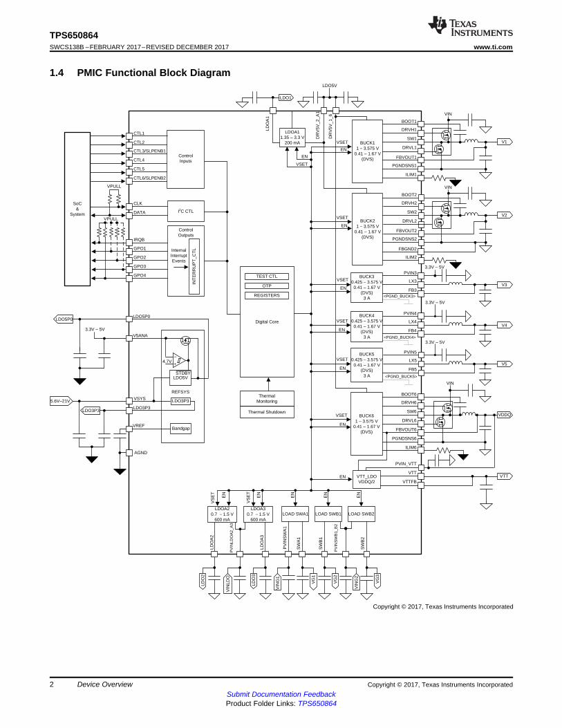
1.4 PMIC Functional Block Diagram

3
TPS650864www.ti.com SWCS138B –FEBRUARY 2017–REVISED DECEMBER 2017
Submit Documentation FeedbackProduct Folder Links: TPS650864
Revision HistoryCopyright © 2017, Texas Instruments Incorporated
Table of Contents1 Device Overview ......................................... 1
1.1 Features .............................................. 11.2 Applications........................................... 11.3 Description............................................ 11.4 PMIC Functional Block Diagram ..................... 2
2 Revision History ......................................... 33 Device Comparison Table.............................. 54 Pin Configuration and Functions..................... 6
4.1 Pin Functions ......................................... 65 Specifications ............................................ 9
5.1 Absolute Maximum Ratings .......................... 95.2 ESD Ratings.......................................... 95.3 Recommended Operating Conditions............... 105.4 Thermal Information................................. 105.5 Electrical Characteristics: Total Current
Consumption ........................................ 105.6 Electrical Characteristics: Reference and Monitoring
System .............................................. 115.7 Electrical Characteristics: Buck Controllers ......... 125.8 Electrical Characteristics: Synchronous Buck
Converters........................................... 135.9 Electrical Characteristics: LDOs .................... 145.10 Electrical Characteristics: Load Switches ........... 165.11 Digital Signals: I2C Interface ........................ 175.12 Digital Input Signals (CTLx) ......................... 175.13 Digital Output Signals (IRQB, GPOx) ............... 175.14 Timing Requirements ............................... 175.15 Switching Characteristics ........................... 18
5.16 Typical Characteristics .............................. 196 Detailed Description ................................... 21
6.1 Overview ............................................ 216.2 Functional Block Diagram........................... 226.3 TPS65086401 Design and Settings................. 246.4 TPS65086470 Design and Settings................. 286.5 SMPS Voltage Regulators .......................... 326.6 LDOs and Load Switches ........................... 396.7 Power Goods (PGOOD or PG) and GPOs ......... 406.8 Power Sequencing and VR Control ................. 426.9 Device Functional Modes ........................... 476.10 I2C Interface ......................................... 476.11 Register Maps ....................................... 51
7 Applications, Implementation, and Layout........ 937.1 Application Information.............................. 937.2 Typical Application .................................. 937.3 Power Supply Coupling and Bulk Capacitors...... 1047.4 Do's and Don'ts ................................... 104
8 Device and Documentation Support .............. 1058.1 Device Support .................................... 1058.2 Documentation Support............................ 1058.3 Receiving Notification of Documentation Updates. 1058.4 Community Resources............................. 1058.5 Trademarks ........................................ 1058.6 Electrostatic Discharge Caution ................... 1068.7 Glossary............................................ 106
9 Mechanical, Packaging, and OrderableInformation ............................................. 106
2 Revision HistoryNOTE: Page numbers for previous revisions may differ from page numbers in the current version.
Changes from Revision A (November 2017) to Revision B Page
• Changed TPS65086401 from preview to production data ...................................................................... 5
Changes from Original (February 2017) to Revision A Page
• Added pin connection when unused ............................................................................................... 7• Changed the TPS65086401 Power Map Example in the TPS65086401 Design and Settings section ................. 24• Fixed SWB1 and SWB2 current to 0.4A from 0.3A ............................................................................ 28• Changed typo from TPS6508470 to TPS65086470 ............................................................................ 31• Changed description to Sleep State from Connected Standby for consistency in the Sleep State Entry and Exit
section ................................................................................................................................ 46• Changed the description of all PGOODs in the note in the Sleep State Entry and Exit section from stay to can
stay because the behavior can vary based on the part-number specific settings .......................................... 46• Added failure to reach power good within 10 ms as emergency shutdown condition to the Emergency Shutdown
section ................................................................................................................................ 46• Changed bit 0 in the BUCK3VID Register register to Read only (R) ........................................................ 57• Changed the PG_DELAY2: 2nd Power Good Delay Register description from GPO3 to GPO1, GPO2, and GPO4 . 70• Fixed a typo which showed the '000' option resulting in 2.5 ms instead of 0 ms in the PG_DELAY2 Register
Descriptions table ................................................................................................................... 70• Fixed a typo which showed the '000' option resulting in 2.5 ms instead of 0 ms in the PG_DELAY2 Register

4
TPS650864SWCS138B –FEBRUARY 2017–REVISED DECEMBER 2017 www.ti.com
Submit Documentation FeedbackProduct Folder Links: TPS650864
Revision History Copyright © 2017, Texas Instruments Incorporated
Descriptions table ................................................................................................................... 70

5
TPS650864www.ti.com SWCS138B –FEBRUARY 2017–REVISED DECEMBER 2017
Submit Documentation FeedbackProduct Folder Links: TPS650864
Pin Configuration and FunctionsCopyright © 2017, Texas Instruments Incorporated
(1) Indicates the original intent of the part number. Parts can be used for alternate applications.
3 Device Comparison Table
Table 3-1 lists a brief summary of the default values for each part number stored in one-timeprogrammable (OTP) memory. A full summary of each part number can be found in the applicationssection linked in the SECTION column. The step size is indicated by the values in parenthesis. If alternatevoltages are available through pin-strapping, they are separated with a comma.
Table 3-1. Default Values
PART NUMBER APPLICATION (1) BUCK1 BUCK2 BUCK3 BUCK4 BUCK5 BUCK6 LDOA1 LDOA2 LDOA3 SECTION
TPS65086401 Xilinx ZynqUltrascale+
1.8 V(25 mV)
0.85 V(10 mV)
0.85 V(25 mV)
3.3 V(25 mV)
3.3 V(25 mV)
1.5 V, 1.2 V,1.1 V
(10 mV)1.8 V 1.2 V 1.2 V Section 6.3
TPS65086470 XilinxArtix 7
1 V(10 mV)
1.8 V(25 mV)
1.2 V(25 mV)
2.5 V(25 mV)
3.3 V(25 mV)
1.35 V, 1.5 V(25 mV) 1.8 V 0.7 V 0.7 V Section 6.4

64IL
IM2
17S
WB
1
1FBGND2 48 VTTFB
63C
TL5
18P
VIN
SW
B1_
B2
2FBVOUT2 47 VTT
62C
TL4
19S
WB
2
3DRVH2 46 PVINVTT
61C
TL3
/SLP
EN
B1
20LX
5
4SW2 45 ILIM6
60C
TL2
21P
VIN
5
5BOOT2 44 FBVOUT6
59D
AT
A22
FB
5
6PGNDSNS2 43 DRVH6
58C
LK23
FB
4
7DRVL2 42 SW6
57V
5AN
A24
PV
IN4
8DRV5V_2_A1 41 BOOT6
56LD
O5P
025
LX4
9LDOA1 40 PGNDSNS6
55V
SY
S26
GP
O2
10LX3 39 DRVL6
54LD
O3P
327
GP
O3
11PVIN3 38 DRV5V_1_6
53V
RE
F28
GP
O4
12FB3 37 DRVL1
52A
GN
D29
FB
VO
UT
1
13CTL1 36 PGNDSNS1
51LD
OA
230
ILIM
1
14CTL6/SLPENB2 35 BOOT1
50P
VIN
LDO
A2_
A3
31S
WA
1
15IRQB 34 SW1
49LD
OA
332
PV
INS
WA
1
16GPO1 33 DRVH1
Not to scale
Thermal
Pad
6
TPS650864SWCS138B –FEBRUARY 2017–REVISED DECEMBER 2017 www.ti.com
Submit Documentation FeedbackProduct Folder Links: TPS650864
Pin Configuration and Functions Copyright © 2017, Texas Instruments Incorporated
4 Pin Configuration and Functions
Figure 4-1 shows the 64-pin RSK Plastic Quad Flatpack No-Lead package.
NOTE: The thermal pad must be connected to the system power ground plane.
Figure 4-1. 64-Pin RSK VQFN With Exposed Thermal Pad (Top View)
4.1 Pin Functions
Pin FunctionsPIN
I/O DESCRIPTIONNO. NAME
SMPS REGULATORS
1 FBGND2 I Remote negative feedback sense for BUCK2 controller. Connect to negative terminal of output capacitor. Connect toground when not in use.

7
TPS650864www.ti.com SWCS138B –FEBRUARY 2017–REVISED DECEMBER 2017
Submit Documentation FeedbackProduct Folder Links: TPS650864
Pin Configuration and FunctionsCopyright © 2017, Texas Instruments Incorporated
Pin Functions (continued)PIN
I/O DESCRIPTIONNO. NAME
2 FBVOUT2 I Remote positive feedback sense for BUCK2 controller. Connect to positive terminal of output capacitor. Connect toground when not in use.
3 DRVH2 O High-side gate driver output for BUCK2 controller. Leave floating when not in use.
4 SW2 I Switch node connection for BUCK2 controller. Connect to ground when not in use.
5 BOOT2 I Bootstrap pin for BUCK2 controller. Connect a 100-nF ceramic capacitor between this pin and SW2 pin. Leave floatingwhen not in use.
6 PGNDSNS2 I Power GND connection for BUCK2. Connect to ground terminal of external low-side FET. Connect to ground when notin use.
7 DRVL2 O Low-side gate driver output for BUCK2 controller. Leave floating when not in use.
8 DRV5V_2_A1 I 5-V supply to BUCK2 gate driver and LDOA1. Bypass to ground with a 2.2-µF (typical) ceramic capacitor. Shorted onboard to LDO5P0 pin typically. Bypass not required if BUCK2 and LDOA1 are not in use.
10 LX3 O Switch node connection for BUCK3 converter. Connect to ground when not in use.
11 PVIN3 I Power input to BUCK3 converter. Bypass to ground with a 10-µF (typical) ceramic capacitor. Bypass not required ifBUCK3 is not in use.
12 FB3 I Remote feedback sense for BUCK3 converter. Connect to positive terminal of output capacitor. Connect to groundwhen not in use.
20 LX5 O Switch node connection for BUCK5 converter. Leave floating when not in use.
21 PVIN5 I Power input to BUCK5 converter. Bypass to ground with a 10-µF (typical) ceramic capacitor. Bypass not required ifBUCK5 is not in use.
22 FB5 I Remote feedback sense for BUCK5 converter. Connect to positive terminal of output capacitor. Connect to groundwhen not in use.
23 FB4 I Remote feedback sense for BUCK4 converter. Connect to positive terminal of output capacitor. Connect to groundwhen not in use.
24 PVIN4 I Power input to BUCK4 converter. Bypass to ground with a 10-µF (typical) ceramic capacitor. Bypass not required ifBUCK4 is not in use.
25 LX4 O Switch node connection for BUCK4 converter. Leave floating when not in use.
29 FBVOUT1 I Remote feedback sense for BUCK1 controller. Connect to positive terminal of output capacitor. Connect to groundwhen not in use.
30 ILIM1 I Current limit set pin for BUCK1 controller. Fit a resistor from this pin to ground to set current limit of external low-sideFET. Connect to ground when BUCK1 not in use.
33 DRVH1 O High-side gate driver output for BUCK1 controller. Leave floating when not in use.
34 SW1 I Switch node connection for BUCK1 controller. Connect to ground when not in use.
35 BOOT1 I Bootstrap pin for BUCK1 controller. Connect a 100-nF ceramic capacitor between this pin and SW1 pin. Leave floatingwhen not in use.
36 PGNDSNS1 I Power GND connection for BUCK1. Connect to ground terminal of external low-side FET. Connect to ground when notin use.
37 DRVL1 O Low-side gate driver output for BUCK1 controller. Leave floating when not in use.
38 DRV5V_1_6 I 5-V supply to BUCK1 and BUCK6 gate drivers. Bypass to ground with a 2.2-µF (typical) ceramic capacitor. Shorted onboard to LDO5P0 pin typically. Bypass not required if BUCK1 and BUCK6 are not in use.
39 DRVL6 O Low-side gate driver output for BUCK6 controller. Leave floating when not in use.
40 PGNDSNS6 I Power GND connection for BUCK6. Connect to ground terminal of external low-side FET. Connect to ground when notin use.
41 BOOT6 I Bootstrap pin for BUCK6 controller. Connect a 100-nF ceramic capacitor between this pin and SW6 pin. Leave floatingwhen not in use.
42 SW6 I Switch node connection for BUCK6 controller. Connect to ground when not in use.
43 DRVH6 O High-side gate driver output for BUCK6 controller. Leave floating when not in use.
44 FBVOUT6 I Remote feedback sense for BUCK6 controller and reference voltage for VTT LDO regulation. Connect to positiveterminal of output capacitor. Connect to ground when not in use.
45 ILIM6 I Current limit set pin for BUCK6 controller. Fit a resistor from this pin to ground to set current limit of external low-sideFET. Connect to ground when BUCK6 not in use.
64 ILIM2 I Current limit set pin for BUCK2 controller. Fit a resistor from this pin to ground to set current limit of external low-sideFET. Connect to ground when BUCK2 not in use.
LDO AND LOAD SWITCHES
9 LDOA1 O LDOA1 output. Bypass to ground with a 4.7-µF (typical) ceramic capacitor. Leave floating when not in use.
17 SWB1 O Output of load switch B1. Bypass to ground with a 0.1-µF (typical) ceramic capacitor. Leave floating when not in use.
18 PVINSWB1_B2 I Power supply to load switch B1 and B2. Bypass to ground with a 1-µF (typical) ceramic capacitor to improve transientperformance. Connect to ground when not in use.

8
TPS650864SWCS138B –FEBRUARY 2017–REVISED DECEMBER 2017 www.ti.com
Submit Documentation FeedbackProduct Folder Links: TPS650864
Pin Configuration and Functions Copyright © 2017, Texas Instruments Incorporated
Pin Functions (continued)PIN
I/O DESCRIPTIONNO. NAME
19 SWB2 O Output of load switch B2. Bypass to ground with a 0.1-µF (typical) ceramic capacitor. Leave floating when not in use.
31 SWA1 O Output of load switch A1. Bypass to ground with a 0.1-µF (typical) ceramic capacitor. Leave floating when not in use.
32 PVINSWA1 I Power supply to load switch A1. Bypass to ground with a 1-µF (typical) ceramic capacitor to improve transientperformance. Connect to ground when not in use.
46 PVINVTT I Power supply to VTT LDO. Bypass to ground with a 10-µF (minimum) ceramic capacitor. Bypass not required if VTTLDO is not in use.
47 VTT O Output of load VTT LDO. Bypass to ground with 2× 22-µF (minimum) ceramic capacitors. Leave floating when not inuse.
48 VTTFB I Remote feedback sense for VTT LDO. Connect to positive terminal of output capacitor. Connect to ground when not inuse.
49 LDOA3 O Output of LDOA3. Bypass to ground with a 4.7-µF (typical) ceramic capacitor. Leave floating when not in use.
50 PVINLDOA2_A3 I Power supply to LDOA2 and LDOA3. Bypass to ground with a 4.7-µF (typical) ceramic capacitor. Connect to groundwhen not in use.
51 LDOA2 O Output of LDOA2. Bypass to ground with a 4.7-µF (typical) ceramic capacitor. Leave floating when not in use.
54 LDO3P3 O Output of 3.3-V internal LDO. Bypass to ground with a 4.7-µF (typical) ceramic capacitor.
56 LDO5P0 O Output of 5-V internal LDO or an internal switch that connects this pin to V5ANA. Bypass to ground with a 4.7-µF(typical) ceramic capacitor.
57 V5ANA IBias used by converters (BUCK3, BUCK4, and BUCK5) for regulation. Must be same supply as PVINx. Also has aninternal load switch that connects this pin to LDO5P0 pin if 5-V is used. Bypass this pin with an optional ceramiccapacitor to improve transient performance.
INTERFACE
13 CTL1 I Active-high VR enable pin. A group of VRs can be assigned to be enabled at assertion or disabled at deassertion ofthis pin.
14 CTL6/SLPENB2 IActive-high VR enable pin. A group of VRs can be assigned to be enabled at assertion or disabled at deassertion ofthis pin. Alternatively, when configured to active-low sleep enable, a group of VRs chosen can be entered into (L) or outof (H) sleep state where their output voltages may be different from those in normal state.
15 IRQB O Open-drain output interrupt pin. Refer to Section 6.11.4, IRQ: PMIC Interrupt Register, for definitions.
16 GPO1 OGeneral purpose output that can be configured to either open-drain or push-pull arrangement. Regardless of theconfiguration, the pin can be programmed either to reflect Power Good status of VRs of any choice or to be controlledby an I2C register bit by the user, which then can be used as an enable signal to an external VR.
26 GPO2 OGeneral purpose output that can be configured to either open-drain or push-pull arrangement. Regardless of theconfiguration, the pin can be programmed either to reflect Power Good status of VRs of any choice or to be controlledby an I2C register bit by the user, which then can be used as an enable signal to an external VR.
27 GPO3 OGeneral purpose output that can be configured to either open-drain or push-pull arrangement. Regardless of theconfiguration, the pin can be programmed either to reflect Power Good status of VRs of any choice or to be controlledby an I2C register bit by the user, which then can be used as an enable signal to an external VR.
28 GPO4 O Open-drain output that can be configured to reflect Power Good status of VRs of any choice or to be controlled by anI2C register bit by the user, which then can be used as an enable signal to an external VR.
58 CLK I I2C clock
59 DATA I/O I2C data
60 CTL2 I Active-high VR enable pin. A group of VRs can be assigned to be enabled at assertion or disabled at deassertion ofthis pin.
61 CTL3/SLPENB1 IActive-high VR enable pin. A group of VRs can be assigned to be enabled at assertion or disabled at deassertion ofthis pin. Alternatively, when configured to active-low sleep enable, a group of VRs chosen can be entered into (L) or outof (H) sleep state where their output voltages may be different from those in normal state.
62 CTL4 I Active-high VR enable pin. A group of VRs can be assigned to be enabled at assertion or disabled at deassertion ofthis pin.
63 CTL5 I Active-high VR enable pin. A group of VRs can be assigned to be enabled at assertion or disabled at deassertion ofthis pin.
REFERENCE
52 AGND — Analog ground. Do not connect to the thermal pad ground on top layer. Connect to ground of VREF capacitor.
53 VREF O Band-gap reference output. Stabilize it by connecting a 100-nF (typical) ceramic capacitor between this pin and quietground.
55 VSYS I System voltage detection and input to internal LDOs (3.3 V and 5 V). Bypass to ground with a 1-µF (typical) ceramiccapacitor.
THERMAL PAD
— Thermal pad(PGND) — Connect to PCB ground plane using multiple vias for good thermal and electrical performance.

9
TPS650864www.ti.com SWCS138B –FEBRUARY 2017–REVISED DECEMBER 2017
Submit Documentation FeedbackProduct Folder Links: TPS650864
SpecificationsCopyright © 2017, Texas Instruments Incorporated
(1) Stresses beyond those listed under Absolute Maximum Ratings may cause permanent damage to the device. These are stress ratingsonly, and functional operation of the device at these or any other conditions beyond those indicated under Recommended OperatingConditions is not implied. Exposure to absolute-maximum-rated conditions for extended periods may affect device reliability.
(2) Transient for less than 5 ns(3) Transient for less than 20 ns
5 Specifications
5.1 Absolute Maximum Ratingsover operating free-air temperature range (unless otherwise noted) (1)
MIN MAX UNITANALOGInput voltage from battery, VSYS –0.3 28 VPVIN3, PVIN4, PVIN5, LDO5P0, DRV5V_1_6, DRV5V_2_A1, DRVL1, DRVL2, DRVL6 –0.3 7 VV5ANA –0.3 6 VPGNDSNS1, PGNDSNS2, PGNDSNS6, AGND, FBGND2 –0.3 0.3 VDRVH1, DRVH2, DRVH6, BOOT1, BOOT2, BOOT6 –0.3 34 VSW1, SW2, SW6 –5 (2) 28 VLX3, LX4, LX5 –2 (3) 8 VDifferential voltage, BOOTx to SWx –0.3 5.5 VVREF, LDO3P3, FBVOUT1, FBVOUT2, FBVOUT6, FB3, FB4, FB5, ILIM1, ILIM2, ILIM6,PVINVTT, VTT, VTTFB, PVINSWA1, SWA1, PVINSWB1_B2, SWB1, SWB2, LDOA1 –0.3 3.6 V
PVINLDOA2_A3, LDOA2, LDOA3 –0.3 3.3 VDIGITAL IODATA, CLK, GPO1-GPO3 –0.3 3.6 VCTL1-CTL6, GPO4, IRQB –0.3 7 VStorage temperature, Tstg –40 150 °C
(1) JEDEC document JEP155 states that 500-V HBM allows safe manufacturing with a standard ESD control process.(2) JEDEC document JEP157 states that 250-V CDM allows safe manufacturing with a standard ESD control process.
5.2 ESD RatingsVALUE UNIT
VESD Electrostatic dischargeHuman Body Model (HBM), per ANSI/ESDA/JEDEC JS001 (1) ±1000
VCharged Device Model (CDM), per JESD22-C101 (2) ±250

10
TPS650864SWCS138B –FEBRUARY 2017–REVISED DECEMBER 2017 www.ti.com
Submit Documentation FeedbackProduct Folder Links: TPS650864
Specifications Copyright © 2017, Texas Instruments Incorporated
5.3 Recommended Operating Conditionsover operating free-air temperature range (unless otherwise noted)
MIN NOM MAX UNITANALOGVSYS 5.6 13 21 VVREF –0.3 1.3 VPVIN3, PVIN4, PVIN5, LDO5P0, V5ANA, DRV5V_1_6, DRV5V_2_A1 –0.3 5.5 VPGNDSNS1, PGNDSNS2, PGNDSNS6, AGND, FBGND2 –0.3 0.3 VDRVH1, DRVH2, DRVH6, BOOT1, BOOT2, BOOT6 –0.3 26.5 vDRVL1, DRVL2, DRVL6 –0.3 5.5 VSW1, SW2, SW6 –1 21 VLX3, LX4, LX5 –1 5.5 VFBVOUT1, FBVOUT2, FBVOUT6, FB3, FB4, FB5 –0.3 3.6 VLDO3P3, ILIM1, ILIM2, ILIM6, LDOA1 –0.3 3.3 VPVINVTT –0.3 BUCK6 FBVOUT6 V
VTT, VTTFB –0.3 0.5 ×FBVOUT6 V
PVINSWA1, SWA1, PVINSWB1_B2, SWB1, SWB2 –0.3 3.6 VPVINLDOA2_A3 –0.3 1.8 VLDOA2, LDOA3 –0.3 1.5 VDIGITAL IODATA, CLK, CTL1–CTL6, GPO1–GPO4, IRQB –0.3 3.3 VCHIPOperating ambient temperature, TA –40 27 85 °COperating junction temperature, TJ –40 27 125 °C
(1) For more information about traditional and new thermal metrics, see Semiconductor and IC Package Thermal Metrics application report.
5.4 Thermal Information
THERMAL METRIC (1)TPS650864xx
UNITRSK (VQFN)64 PINS
RθJA Junction-to-ambient thermal resistance 25.8 °C/WRθJC(top) Junction-to-case (top) thermal resistance 11.3 °C/WRθJB Junction-to-board thermal resistance 4.4 °C/WψJT Junction-to-top characterization parameter 0.2 °C/WψJB Junction-to-board characterization parameter 4.4 °C/WRθJC(bot) Junction-to-case (bottom) thermal resistance 0.7 °C/W
5.5 Electrical Characteristics: Total Current Consumptionover recommended free-air temperature range and over recommended input voltage range (typical values are at TA = 25°C)(unless otherwise noted)
PARAMETER TEST CONDITIONS MIN TYP MAX UNIT
ISDPMIC shutdown current that includes IQ forreferences, LDO5, LDO3P3, and digital core
VSYS = 13 V, all functional output railsare disabled 65 µA

11
TPS650864www.ti.com SWCS138B –FEBRUARY 2017–REVISED DECEMBER 2017
Submit Documentation FeedbackProduct Folder Links: TPS650864
SpecificationsCopyright © 2017, Texas Instruments Incorporated
5.6 Electrical Characteristics: Reference and Monitoring Systemover recommended free-air temperature range and over recommended input voltage range (typical values are at TA = 25°C)(unless otherwise noted)
PARAMETER TEST CONDITIONS MIN TYP MAX UNITREFERENCE
VREFBand-gap reference voltage 1.25 VAccuracy –0.5% 0.5%
CVREF Band-gap output capacitor 0.047 0.1 0.22 µFVSYS_UVLO_5V VSYS UVLO threshold for LDO5 VSYS falling 5.24 5.4 5.56 V
VSYS_UVLO_5V_HYSVSYS UVLO threshold hysteresis forLDO5
VSYS rising aboveVSYS_UVLO_5V
200 mV
VSYS_UVLO_3V VSYS UVLO threshold for LDO3P3 VSYS falling 3.45 3.6 3.75 V
VSYS_UVLO_3V_HYSVSYS UVLO threshold hysteresis forLDO3P3
VSYS rising aboveVSYS_UVLO_3V
150 mV
TCRIT Critical threshold of die temperature TJ rising 130 145 160 °CTCRIT_HYS Hysteresis of TCRIT TJ falling 10 °CTHOT Hot threshold of die temperature TJ rising 110 115 120 °CTHOT_HYS Hysteresis of THOT TJ falling 10 °CLDO5VIN Input voltage at VSYS pin 5.6 13 21 VVOUT DC output voltage IOUT = 10 mA 4.9 5 5.1 VIOUT DC output current 100 180 mA
IOCP Overcurrent protection Measured with output shorted toground 200 mA
VTH_PGPower Good assertion threshold inpercentage of target VOUT
VOUT rising 94%
VTH_PG_HYS Power Good deassertion hysteresis VOUT rising or falling 4%IQ Quiescent current VIN = 13 V, IOUT = 0 A 20 µACOUT External output capacitance 2.7 4.7 10 µFV5ANA-to-LDO5P0 LOAD SWITCH
RDSON On resistanceVIN = 5 V, measured fromV5ANA pin to LDO5P0 pin atIOUT = 200 mA
1 Ω
VTH_PGPower Good threshold for external 5-V supply VV5ANA rising 4.7 V
VTH_HYS_PGPower Good threshold hysteresis forexternal 5-V supply VV5ANA falling 100 mV
ILKG Leakage current Switch disabled,VV5ANA = 5 V, VLDO5 = 0 V 10 µA
LDO3P3VIN Input voltage at VSYS pin 5.6 13 21 V
VOUT
DC output voltage IOUT = 10 mA 3.3 V
Accuracy VIN = 13 V,IOUT = 10 mA –3% 3%
IOUT DC output current 40 mA
IOCP Overcurrent protection Measured with output shorted toground 70 mA
VTH_PGPower Good assertion threshold inpercentage of target VOUT
VOUT rising 92%
VTH_PG_HYS Power Good deassertion hysteresis VOUT falling 3%
IQ Quiescent current VIN = 13 V,IOUT = 0 A 20 µA
COUT External output capacitance 2.2 4.7 10 µF

12
TPS650864SWCS138B –FEBRUARY 2017–REVISED DECEMBER 2017 www.ti.com
Submit Documentation FeedbackProduct Folder Links: TPS650864
Specifications Copyright © 2017, Texas Instruments Incorporated
(1) BUCKx_VID[6:0] = 0000001 – 0011000
5.7 Electrical Characteristics: Buck Controllersover recommended input voltage range, TA = –40°C to +85°C and TA = 25°C for typical values (unless otherwise noted)
PARAMETER TEST CONDITIONS MIN TYP MAX UNITBUCK1, BUCK2, BUCK6
VINPower input voltage forexternal HSD FET 5.6 13 21 V
VOUT
DC output voltage VIDrange and options
VID step size = 10 mV, BUCKx_VID[6:0]progresses from 0000001 to 1111111 0.41 See
Section 3 1.67 V
VID step size = 25 mV, BUCKx_VID[6:0]progresses from 0000001 to 1111111 1 (1) See
Section 3 3.575 V
DC output voltageaccuracy
VOUT = 1, 1.2, 1.35, 1.5, 1.8, 2.5, 3.3 V,IOUT = 100 mA to 7 A –2% 2%
Total output voltageaccuracy (DC + ripple) inDCM
IOUT = 10 mA, VOUT ≤ 1 V –30 40 mV
VFB_EXT_BUCK1Feedback regulationvoltage
Applies only to the Buck1 Controller if configuredfor external feedback voltage adjustability 384 400 416 mV
IFB_LKG_BUCK1Feedback pin leakagecurrent
Applies only to the Buck1 Controller if configuredfor external feedback voltage adjustability 65 nA
SR(VOUT) Output DVS slew rateVID step size = 10 mV 2.5 3.125
mV/µsVID step size = 25 mV 3.125 4
ILIM_LSD
Low-side output valleycurrent limit accuracy(programmed by externalresistor RLIM)
–15% 15%
ILIMREFSource current out ofILIM1 pin T = 25°C 45 50 55 µA
VLIM Voltage at ILIM1 pin VLIM = RLIM × ILIMREF 0.2 2.25 V
ΔVOUT/ΔVIN Line regulation VOUT = 1, 1.2, 1.35, 1.5, 1.8, 2.5, 3.3 V,IOUT = 7 A –0.5% 0.5%
ΔVOUT/ΔIOUT Load regulationVIN = 13 V, VOUT = 1, 1.2, 1.35, 1.5, 1.8, 2.5,3.3 V, IOUT = 0 A to 7 A,referenced to VOUT at IOUT = IOUT_MAX
0% 1%
VTH_PG
Power Good deassertionthreshold in percentageof target VOUT
VOUT rising 105.5% 108% 110.5%
VOUT falling 89.5% 92% 94.5%
RDSON_DRVH Driver DRVH resistanceSource, IDRVH = –50 mA 3 Ω
Sink, IDRVH = 50 mA 2 Ω
RDSON_DRVL Driver DRVL resistanceSource, IDRVL = –50 mA 3 Ω
Sink, IDRVL = 50 mA 0.4 Ω
RDISOutput auto-dischargeresistance
BUCKx_DISCHG[1:0] = 01 100 Ω
BUCKx_DISCHG[1:0] = 10 200 Ω
BUCKx_DISCHG[1:0] = 11 500 Ω
CBOOT Bootstrap capacitance 100 nF
RON_BOOTBootstrap switch ONresistance 20 Ω

13
TPS650864www.ti.com SWCS138B –FEBRUARY 2017–REVISED DECEMBER 2017
Submit Documentation FeedbackProduct Folder Links: TPS650864
SpecificationsCopyright © 2017, Texas Instruments Incorporated
5.8 Electrical Characteristics: Synchronous Buck Convertersover recommended input voltage range, TA = –40°C to +85°C and TA = 25°C for typical values (unless otherwise noted)
PARAMETER TEST CONDITIONS MIN TYP MAX UNITBUCK3, BUCK4, BUCK5VIN Power input voltage 3.0 5.5 V
VOUT
DC output voltage VID rangeand options
VID step size = 10 mV,BUCKx_VID[6:0] progresses from0000001 to 1111111
0.41 SeeSection 3 1.67
VVID step size = 25 mV,BUCKx_VID[6:0] progresses from0000001 to 1111111
0.425 SeeSection 3 3.575
DC output voltage accuracy
VIN = 5.0V, VOUT = 1, 1.2, 1.35, 1.5,1.8, 2.5, 3.3 V,IOUT = 1.5 A
–2% 2%
VIN = 3.3V, VOUT = 1, 1.2, 1.35, 1.5,1.8 V,IOUT = 1.5 A
–2% 2%
VIN = 5.0V, VOUT = 1, 1.2, 1.35, 1.5,1.8 V, 2.5, 3.3 V,IOUT = 100 mA
–2.5% 2.5%
%VIN = 3.3V, VOUT = 1, 1.2, 1.35, 1.5,1.8 V,IOUT = 100 mA
–2.5% 2.5%
Total output voltage accuracy(DC + ripple) in DCM
VIN = 5.0V, IOUT = 10 mA, VOUT ≤ 1V –30 40 mV
SR(VOUT) Output DVS slew rateVID step size = 10 mV 2.5 3.125
mV/µsVID step size = 25 mV 3.125 4
IOUT Continuous DC output current 3 AIIND_LIM HSD FET current limit 4.3 7 AIQ Quiescent current VIN = 5 V, VOUT = 1 V 35 µA
ΔVOUT/ΔVIN Line regulation VOUT = 1, 1.2, 1.35, 1.5, 1.8,2.5, 3.3 V, IOUT = 1.5 A –0.5% 0.5%
ΔVOUT/ΔIOUT Load regulation
VIN = 5 V, VOUT = 1, 1.2, 1.35, 1.5,1.8, 2.5, 3.3 V,IOUT = 0 A to 3 A, referenced toVOUT at IOUT = 1.5 A
–0.2% 2%
VTH_PG
Power Good deassertionthreshold in percentage oftarget VOUT
VOUT rising 108%
VOUT falling 92%
VTH_HYS_PG
Power Good reassertionhysteresis entering back intoVTH_PG
VOUT rising or falling 3%
RDISOutput auto-dischargeresistance
BUCKx_DISCHG[1:0] = 01 100ΩBUCKx_DISCHG[1:0] = 10 200
BUCKx_DISCHG[1:0] = 11 500

14
TPS650864SWCS138B –FEBRUARY 2017–REVISED DECEMBER 2017 www.ti.com
Submit Documentation FeedbackProduct Folder Links: TPS650864
Specifications Copyright © 2017, Texas Instruments Incorporated
(1) The minimum value must be equal to or greater than 1.62 V.
5.9 Electrical Characteristics: LDOsover recommended input voltage range, TA = –40°C to +85°C and TA = 25°C for typical values (unless otherwise noted)
PARAMETER TEST CONDITIONS MIN TYP MAX UNITLDOA1VIN Input voltage 4.5 5 5.5 V
VOUTDC output voltage Set by LDOA1_VID[3:0] 1.35 See
Section 3 3.3 V
Accuracy IOUT = 0 to 200 mA –2% 2% VIOUT DC output current 200 mAΔVOUT/ΔVIN Line regulation IOUT = 40 mA –0.5% 0.5%ΔVOUT/ΔIOUT Load regulation IOUT = 10 mA to 200 mA –2% 2%
IOCP Overcurrent protection VIN = 5 V, Measured with outputshorted to ground 500 mA
VTH_PG
Power Good deassertionthreshold in percentage oftarget VOUT
VOUT rising 108%
VOUT falling 92%
tSTARTUP Start-up timeMeasured from EN = H to reach 95%of final value,COUT = 4.7 µF
500 µs
IQ Quiescent current IOUT = 0 A 23 µA
COUTExternal output capacitance 2.7 4.7 10 µFESR 100 mΩ
RDISOutput auto-dischargeresistance
LDOA1_DISCHG[1:0] = 01 100 Ω
LDOA1_DISCHG[1:0] = 10 190 Ω
LDOA1_DISCHG[1:0] = 11 450 Ω
LDOA2 and LDOA3VIN Power input voltage VOUT + VDROP
(1) 1.8 1.98 V
VOUT
LDOA2 DC output voltage Set by LDOA2_VID[3:0] 0.7 SeeSection 3 1.5 V
LDOA3 DC output voltage Set by LDOA3_VID[3:0] 0.7 SeeSection 3 1.5 V
DC output voltage accuracy IOUT = 0 to 600 mA –2% 3%IOUT DC output current 600 mA
VDROP Dropout voltage VOUT = 0.99 × VOUT_NOM,IOUT = 600 mA 350 mV
ΔVOUT/ΔVIN Line regulation IOUT = 300 mA –0.5% 0.5%ΔVOUT/ΔIOUT Load regulation IOUT = 10 mA to 600 mA –2% 2%
IOCP Overcurrent protection Measured with output shorted toground 0.65 1.25 A
VTH_PG
Power Good assertionthreshold in percentage oftarget VOUT
VOUT rising 108%
VOUT falling 92%
tSTARTUP Start-up time Measured from EN = H to reach 95%of final value, COUT = 4.7 µF 500 µs
IQ Quiescent current IOUT = 0 A 20 µA
PSRR Power supply rejection ratio
f = 1 kHz, VIN = 1.8 V, VOUT = 1.2 V,IOUT = 300 mA,COUT = 2.2 µF – 4.7 µF
48 dB
f = 10 kHz, VIN = 1.8 V, VOUT = 1.2 V,IOUT = 300 mA,COUT = 2.2 µF – 4.7 µF
30 dB
COUTExternal output capacitance 2.2 4.7 10 µFESR 100 mΩ

15
TPS650864www.ti.com SWCS138B –FEBRUARY 2017–REVISED DECEMBER 2017
Submit Documentation FeedbackProduct Folder Links: TPS650864
SpecificationsCopyright © 2017, Texas Instruments Incorporated
Electrical Characteristics: LDOs (continued)over recommended input voltage range, TA = –40°C to +85°C and TA = 25°C for typical values (unless otherwise noted)
PARAMETER TEST CONDITIONS MIN TYP MAX UNIT
RDISOutput auto-dischargeresistance
LDOA[2,3]_DISCHG[1:0] = 01 80ΩLDOA[2,3]_DISCHG[1:0] = 10 180
LDOA[2,3]_DISCHG[1:0] = 11 475VTT LDOVIN Power input voltage 1.2 3.3 V
VOUT
DC output voltage VIN = 1.2 V, Measured at VTTFB pin VIN / 2 V
DC output voltage accuracy
Relative to VIN / 2, IOUT ≤ 10 mA,1.1 V ≤ VIN ≤ 1.35 V –10 10
mVRelative to VIN / 2, IOUT ≤ 500 mA,1.1 V ≤ VIN ≤ 1.35 V –25 25
IOUT
DC Output Current (RMSValue Over Operation) 1.1 V ≤ VIN ≤ 1.5 V –500 0 500 mA
Pulsed Current (Duty CycleLimited to Remain Below DCRMS Specification)
source(+) and sink(–): IOCP = 0.95 A,1.1 V ≤ VIN ≤ 1.5 V –500 500
mAsource(+) and sink(–): IOCP = 1.8 A,1.1 V ≤ VIN ≤ 1.5 V –1800 1800
ΔVOUT/ΔIOUT Load regulation
Relative to VIN / 2, IOUT ≤ 10 mA,1.1 V ≤ VIN ≤ 1.5 V –10 10
mV
Relative to VIN / 2, IOUT ≤ 500 mA,1.1 V ≤ VIN ≤ 1.5 V –20 20
Relative to VIN / 2, IOUT ≤ 1200 mA,1.1 V ≤ VIN ≤ 1.5 V –30 30
Relative to VIN / 2, IOUT ≤ 1800 mA,1.1 V ≤ VIN ≤ 1.5 V –40 40
ΔVOUT_TR Load transient regulation
DC + AC at sense point, 1.1 V ≤ VIN≤ 1.5 V,(IOUT = 0 to 350 mA and 350 mA to0) AND(0 to –350 mA and –350 mA to 0)with 1 µs of rise and fall timeCOUT = 40 µF
–5% 5%
IOCP Overcurrent protection
Measured with output shorted toground: OTPs with VTT ILIM = 0.95 A 0.95
AMeasured with output shorted toground: OTPs with VTT ILIM = 1.8 A 1.8
VTH_PG
Power Good deassertionthreshold in percentage oftarget VOUT
VOUT rising 110%
VOUT falling 95%
VTH_HYS_PG
Power Good reassertionhysteresis entering back intoVTH_PG
5%
IQ Total ground current VIN = 1.2 V, IOUT = 0 A 240 µAILKG OFF leakage current VIN = 1.2 V, disabled 1 µACIN External input capacitance 10 µFCOUT External output capacitance 35 µF
RDISOutput auto-dischargeresistance
VTT_DISCHG = 0 1000 kΩVTT_DISCHG = 1 60 80 100 Ω
16
TPS650864SWCS138B –FEBRUARY 2017–REVISED DECEMBER 2017 www.ti.com
Submit Documentation FeedbackProduct Folder Links: TPS650864
Specifications Copyright © 2017, Texas Instruments Incorporated
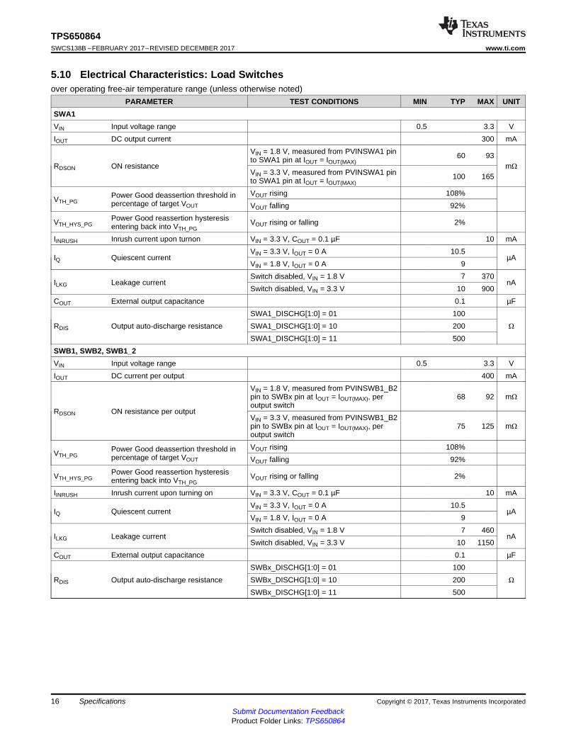
5.10 Electrical Characteristics: Load Switchesover operating free-air temperature range (unless otherwise noted)
PARAMETER TEST CONDITIONS MIN TYP MAX UNITSWA1VIN Input voltage range 0.5 3.3 VIOUT DC output current 300 mA
RDSON ON resistance
VIN = 1.8 V, measured from PVINSWA1 pinto SWA1 pin at IOUT = IOUT(MAX)
60 93mΩ
VIN = 3.3 V, measured from PVINSWA1 pinto SWA1 pin at IOUT = IOUT(MAX)
100 165
VTH_PGPower Good deassertion threshold inpercentage of target VOUT
VOUT rising 108%VOUT falling 92%
VTH_HYS_PGPower Good reassertion hysteresisentering back into VTH_PG
VOUT rising or falling 2%
IINRUSH Inrush current upon turnon VIN = 3.3 V, COUT = 0.1 µF 10 mA
IQ Quiescent currentVIN = 3.3 V, IOUT = 0 A 10.5
µAVIN = 1.8 V, IOUT = 0 A 9
ILKG Leakage currentSwitch disabled, VIN = 1.8 V 7 370
nASwitch disabled, VIN = 3.3 V 10 900
COUT External output capacitance 0.1 µF
RDIS Output auto-discharge resistanceSWA1_DISCHG[1:0] = 01 100
ΩSWA1_DISCHG[1:0] = 10 200SWA1_DISCHG[1:0] = 11 500
SWB1, SWB2, SWB1_2VIN Input voltage range 0.5 3.3 VIOUT DC current per output 400 mA
RDSON ON resistance per output
VIN = 1.8 V, measured from PVINSWB1_B2pin to SWBx pin at IOUT = IOUT(MAX), peroutput switch
68 92 mΩ
VIN = 3.3 V, measured from PVINSWB1_B2pin to SWBx pin at IOUT = IOUT(MAX), peroutput switch
75 125 mΩ
VTH_PGPower Good deassertion threshold inpercentage of target VOUT
VOUT rising 108%VOUT falling 92%
VTH_HYS_PGPower Good reassertion hysteresisentering back into VTH_PG
VOUT rising or falling 2%
IINRUSH Inrush current upon turning on VIN = 3.3 V, COUT = 0.1 µF 10 mA
IQ Quiescent currentVIN = 3.3 V, IOUT = 0 A 10.5
µAVIN = 1.8 V, IOUT = 0 A 9
ILKG Leakage currentSwitch disabled, VIN = 1.8 V 7 460
nASwitch disabled, VIN = 3.3 V 10 1150
COUT External output capacitance 0.1 µF
RDIS Output auto-discharge resistanceSWBx_DISCHG[1:0] = 01 100
ΩSWBx_DISCHG[1:0] = 10 200SWBx_DISCHG[1:0] = 11 500
17
TPS650864www.ti.com SWCS138B –FEBRUARY 2017–REVISED DECEMBER 2017
Submit Documentation FeedbackProduct Folder Links: TPS650864
SpecificationsCopyright © 2017, Texas Instruments Incorporated
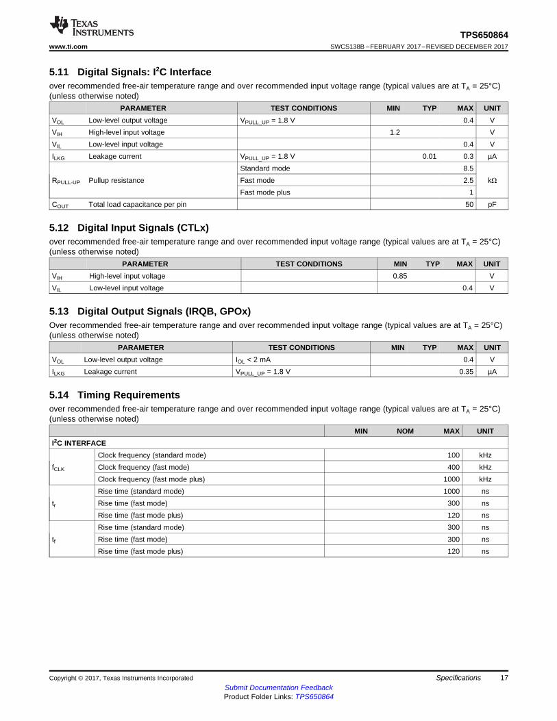
5.11 Digital Signals: I2C Interfaceover recommended free-air temperature range and over recommended input voltage range (typical values are at TA = 25°C)(unless otherwise noted)
PARAMETER TEST CONDITIONS MIN TYP MAX UNITVOL Low-level output voltage VPULL_UP = 1.8 V 0.4 VVIH High-level input voltage 1.2 VVIL Low-level input voltage 0.4 VILKG Leakage current VPULL_UP = 1.8 V 0.01 0.3 µA
RPULL-UP Pullup resistanceStandard mode 8.5
kΩFast mode 2.5Fast mode plus 1
COUT Total load capacitance per pin 50 pF
5.12 Digital Input Signals (CTLx)over recommended free-air temperature range and over recommended input voltage range (typical values are at TA = 25°C)(unless otherwise noted)
PARAMETER TEST CONDITIONS MIN TYP MAX UNITVIH High-level input voltage 0.85 VVIL Low-level input voltage 0.4 V
5.13 Digital Output Signals (IRQB, GPOx)Over recommended free-air temperature range and over recommended input voltage range (typical values are at TA = 25°C)(unless otherwise noted)
PARAMETER TEST CONDITIONS MIN TYP MAX UNITVOL Low-level output voltage IOL < 2 mA 0.4 VILKG Leakage current VPULL_UP = 1.8 V 0.35 µA
5.14 Timing Requirementsover recommended free-air temperature range and over recommended input voltage range (typical values are at TA = 25°C)(unless otherwise noted)
MIN NOM MAX UNITI2C INTERFACE
fCLK
Clock frequency (standard mode) 100 kHzClock frequency (fast mode) 400 kHzClock frequency (fast mode plus) 1000 kHz
tr
Rise time (standard mode) 1000 nsRise time (fast mode) 300 nsRise time (fast mode plus) 120 ns
tf
Rise time (standard mode) 300 nsRise time (fast mode) 300 nsRise time (fast mode plus) 120 ns

18
TPS650864SWCS138B –FEBRUARY 2017–REVISED DECEMBER 2017 www.ti.com
Submit Documentation FeedbackProduct Folder Links: TPS650864
Specifications Copyright © 2017, Texas Instruments Incorporated
5.15 Switching Characteristicsover operating free-air temperature range and over recommended input voltage range (typical values are at TA = 25°C)(unless otherwise noted)
PARAMETER TEST CONDITIONS MIN TYP MAX UNITBUCK CONTROLLERS
tPG Total turnon time Measured from enable going high to when output reaches90% of target value. 550 850 µs
TON,MINMinimum on-time ofDRVH 50 ns
TDEAD Driver dead-timeDRVH off to DRVL on 15 nsDRVL off to DRVH on 30 ns
fSW Switching frequency Continuous-conduction mode,VIN = 13 V, VOUT ≥ 1 V 1000 kHz
BUCK CONVERTERS
tPG Total turnon time Measured from enable going high to when output reaches90% of target value. 250 1000 µs
fSW Switching frequency Continuous-conduction mode See Figure 5-9 MHzLDOAx
tSTARTUP Start-up timeMeasured from enable going high to when output reaches95% of final value,VOUT = 1.2 V, COUT = 4.7 µF
180 µs
VTT LDO
tSTARTUP Start-up time Measured from enable going high to PG assertion,VOUT = 0.675 V, COUT = 40 µF 22 µs
SWA1
tTURN-ON Turnon time
Measured from enable going high to reach 95% of finalvalue,VIN = 3.3 V, COUT = 0.1 µF
0.85 ms
Measured from enable going high to reach 95% of finalvalue,VIN = 1.8 V, COUT = 0.1 µF
0.63 ms
SWB1_2
tTURN-ON Turnon time
Measured from enable going high to reach 95% of finalvalue,VIN = 3.3 V, COUT = 0.1 µF
1.1 ms
Measured from enable going high to reach 95% of finalvalue,VIN = 1.8 V, COUT = 0.1 µF
0.82 ms

Load Current (A)
Effi
cien
cy (
%)
0.1 0.2 0.3 0.4 0.5 0.7 1 2 350%
55%
60%
65%
70%
75%
80%
85%
90%
95%
100%
D013
VOUT = 1 VVOUT = 1.5 VVOUT = 1.8 VVOUT = 2.5 V
Iout (A)
Effi
cien
cy (
%)
0.1 0.2 0.3 0.4 0.5 0.7 1 2 350%
55%
60%
65%
70%
75%
80%
85%
90%
95%
100%
D009
Vout = 1 VVout = 1.8 VVout = 2.5 VVout = 3.3 V
Iout (A)
Effi
cien
cy (
%)
0.1 0.2 0.3 0.40.5 0.7 1 2 3 4 5 6 750%
55%
60%
65%
70%
75%
80%
85%
90%
95%
100%
D011
Vout = 1 VVout = 1.8 VVout = 2.5 VVout = 3.3 V
Iout (A)
Effi
cien
cy (
%)
0.1 0.2 0.3 0.40.5 0.7 1 2 3 4 5 6 750%
55%
60%
65%
70%
75%
80%
85%
90%
95%
100%
D012
Vout = 1 VVout = 1.8 VVout = 2.5 VVout = 3.3 V
19
TPS650864www.ti.com SWCS138B –FEBRUARY 2017–REVISED DECEMBER 2017
Submit Documentation FeedbackProduct Folder Links: TPS650864
SpecificationsCopyright © 2017, Texas Instruments Incorporated
5.16 Typical CharacteristicsMeasurements are taken at 25°C.
FET = CSD87588N L = PIMB061H-R22MSCOUT = 2 × 150 µF + 1 × 22 µF
Figure 5-1. Example BUCK2 Controller Start-Up
L = PIFE32251B-R47MSCOUT = 4 × 22 µF
Figure 5-2. Example BUCK3 Converter Start-Up
FET = CSD87381P L = PIMB061H-R47MS
Figure 5-3. Example BUCK1 Efficiency at VIN = 13 V
FET = CSD87381P L = PIMB061H-R47MS
Figure 5-4. Example BUCK1 Efficiency at VIN = 18 V
L = PIFE32251B-R47MS
Figure 5-5. Example BUCK3 Efficiency at VIN = 5 V
L = PIFE32251B-R47MS
Figure 5-6. Example BUCK3 Efficiency at VIN = 3.3 V

Output Voltage Setting (V)
Sw
itchi
ng F
requ
ency
(M
Hz)
0.4 0.6 0.8 1 1.2 1.4 1.6 1.80
0.5
1
1.5
2
2.5
3
3.5
D016
VIN = 5 VVIN = 3.3 V
Output Voltage Setting (V)
Sw
itchi
ng F
requ
ency
(M
Hz)
0.4 0.8 1.2 1.6 2 2.4 2.8 3.2 3.60
0.5
1
1.5
2
2.5
3
3.5
D017
VIN = 5 VVIN = 3.3 V
Load Current (A)
Mea
sure
d O
utpu
t Vol
tage
(V
)
0 1 2 3 41.5
1.7
1.9
2.1
2.3
2.5
2.7
2.9
D014
VOUT = 1.8 VVOUT = 2.5 VVOUT = 2.8 V
Load Current (A)
Out
put V
olta
ge (
mV
)
-2 -1.5 -1 -0.5 0 0.5 1 1.5 2630
640
650
660
670
680
690
700
710
D015
�40qC25qC85qC
20
TPS650864SWCS138B –FEBRUARY 2017–REVISED DECEMBER 2017 www.ti.com
Submit Documentation FeedbackProduct Folder Links: TPS650864
Specifications Copyright © 2017, Texas Instruments Incorporated
Typical Characteristics (continued)Measurements are taken at 25°C.
L = PIFE32251B-R47MS
Figure 5-7. Converter Load Current Limitations with VIN = 3.3 V
FBVOUT6 = PVINVTT = 1.35 V
Figure 5-8. VTT LDO Regulation
L = PIFE32251B-R47MS
Figure 5-9. Converter Switching Frequency (10-mV Step Size)
L = PIFE32251B-R47MS
Figure 5-10. Converter Switching Frequency (25-mV Step Size)

21
TPS650864www.ti.com SWCS138B –FEBRUARY 2017–REVISED DECEMBER 2017
Submit Documentation FeedbackProduct Folder Links: TPS650864
Detailed DescriptionCopyright © 2017, Texas Instruments Incorporated
(1) When powered from a 5-V supply through the DRV5V_2_A1 pin. Otherwise, max current is limited by max IOUT of LDO5.
6 Detailed Description
6.1 OverviewThe TPS650864xx power-management integrated circuit (PMIC) provides a highly flexible andconfigurable power solution that can power a wide array of processors along with DDR3/DDR4 memoryand other peripherals. Integrated in the PMIC are three step-down controllers (BUCK1, BUCK2, andBUCK6), three step-down converters (BUCK3, BUCK4, and BUCK5), a sink or source LDO (VTT LDO),three low-voltage VIN LDOs (LDOA1–LDOA3), and three load switches (SWA1, SWB1, and SWB2). Withon-chip one-time programmable (OTP) memory, configuration of each rail for default output value, power-up sequence, fault handling, and Power Good mapping into a GPO pin are all conveniently flexible. AllVRs have a built-in discharge resistor, and the value can be changed using theDISCHCNT1–DISCHCNT3 and LDOA1_SWB2_CTRL registers. When enabling a VR, the PMICautomatically disconnects the discharge resistor for that rail without any I2C command. Table 6-1 lists thekey characteristics of the voltage rails.
Table 6-1. Summary of Voltage Regulators
RAIL TYPEINPUT VOLTAGE (V) OUTPUT VOLTAGE RANGE (V)
CURRENT (mA)MIN MAX MIN TYP MAX
BUCK1 Step-down controller 4.5 21 0.41 OTP-programmable 3.575 scalable
BUCK2 Step-down controller 4.5 21 0.41 OTP-programmable 3.575 scalable
BUCK3 Step-down converter 3 5.5 0.41 OTP-programmable 3.575 3000
BUCK4 Step-down Converter 3 5.5 0.41 OTP-programmable 3.575 3000
BUCK5 Step-down converter 3 5.5 0.41 OTP-programmable 3.575 3000
BUCK6 Step-down controller 4.5 21 0.41 OTP-programmable 3.575 scalable
LDOA1 LDO 4.5 5.5 1.35 OTP-programmable 3.3 200 (1)
LDOA2 LDO 1.62 1.98 0.7 OTP-programmable 1.5 600
LDOA3 LDO 1.62 1.98 0.7 OTP-programmable 1.5 600
SWA1 Load switch 0.5 3.3 300
SWB1/SWB2 Load switch 0.5 3.3 400
VTT Sink and source LDO 1.1 1.8 FBVOUT6 / 2 OTP-programmable

VIN
V1
IRQB
ControlOutputs
REGISTERS
Digital Core
INT
ER
RU
PT
_CT
L
ThermalMonitoring
Thermal Shutdown
OTP
TEST CTL
I2C CTL
GPO1
GPO4
GPO2
GPO3
InternalInterrupt Events
BUCK30.425 � 3.575 V0.41 ± 1.67 V
(DVS)3 A
LDOA20.7 � 1.5 V
600 mA
ControlInputs
LOAD SWB2
VPULL
BOOT1
DRVH1
SW1
DRVL1
FBVOUT1
PGNDSNS1
ILIM1
BUCK21 � 3.575 V
0.41 ± 1.67 V (DVS)
BOOT2
DRVH2
SW2
DRVL2
FBVOUT2
PGNDSNS2
ILIM2
PVIN3
LX3
FB3
3.3V ± 5V
PVIN4
LX4
FB4
<PGND_BUCK5>
PVIN5
LX5
FB5
3.3V ± 5V
VIN
BOOT6
DRVH6
SW6
DRVL6
FBVOUT6
PGNDSNS6
ILIM6
VDDQ
VTT
PVIN_VTT
VTT
VTTFB
DR
V5V
_1_6
DR
V5V
_2_A
1
LDO
A1
CLK
DATA
LOAD SWB1LOAD SWA1LDOA3
0.7 � 1.5 V600 mA
SW
B2
PV
INS
WB
1_B
2
SW
B1
SW
A1
LDO
A3
PV
INLD
OA
2_A
3
LDO
A2
LDO
2
LDO
3
V3
V4
V5
FBGND2
VSET
EN
VSET
EN
VSET
EN
VSET
EN
VSET
EN
VSET
EN
VS
ET
EN
VS
ET
EN
EN
EN
EN
EN
EN
LDO1
LDO5V
3.3V ± 5V
CTL4
CTL1
CTL2
CTL3/SLPENB1
CTL5
CTL6/SLPENB2
VPULL
VIN
LDO
VIN
G1
VIN
G2
VG
3
VG
1
VG
2
VTT_LDOVDDQ/2
BUCK61 � 3.575 V
0.41 ± 1.67 V(DVS)
VREF
VSYS
LDO3P3
AGND
LDO5P0LDO5P0
VSET
BUCK11 � 3.575 V
0.41 ± 1.67 V (DVS)
SoC&
System
5.6V±21V
LDO3P3
4.7V
Bandgap
LDO5VSTDBY
LDO3P3
REFSYS
3.3V ± 5VV5ANA
±
+
PV
INS
WA
1
LDOA11.35 ± 3.3 V
200 mA
<PGND_BUCK4>
<PGND_BUCK3>
BUCK50.425 � 3.575 V0.41 ± 1.67 V
(DVS) 3 A
BUCK40.425 � 3.575 V0.41 ± 1.67 V
(DVS) 3 A
VIN
V2
Copyright © 2017, Texas Instruments Incorporated
22
TPS650864SWCS138B –FEBRUARY 2017–REVISED DECEMBER 2017 www.ti.com
Submit Documentation FeedbackProduct Folder Links: TPS650864
Detailed Description Copyright © 2017, Texas Instruments Incorporated
6.2 Functional Block Diagram
Figure 6-1. PMIC Functional Block Diagram

DDR
BUCK1
BUCK2
BUCK3 3A
BUCK4 3A
BUCK5 3A
BUCK6
VTT LDO ±0.5A
LDOA2 0.6A
LDOA3 0.6A
SWA1 0.3A
SWB1 0.3A
SWB2 0.3A
LDO5
LDO3P3
PG_5V
EXT FET
EXT FET
EXT FET
VCORE
VGPU
VCCIO
VCPU1
VCPU2
VDDQ, VDD1&2
VREF, VTT
VSUPP2
VSUPP3
VSUPP4
VSUPP5
PMIC Example SoC PLATFORMVIN
LDO5V
1.8V
5V Supply
VSYS
IRQB
SCL
SDA
GPO1 ± GPO4
VSUPP6
CTL1 ± CTL6
LDOA1 0.2A VSUPP1
Input up to 3.3V
Input up to 3.3V
5V Supply
VIN
VIN
DDR
VDDQ, VDD1&2
VREF, VTT
Note: An LDO or Buck Can Supply the VPP Rail if Needed for DDR.
LDO5V or 5V Supply
VIN
Copyright © 2017, Texas Instruments Incorporated
23
TPS650864www.ti.com SWCS138B –FEBRUARY 2017–REVISED DECEMBER 2017
Submit Documentation FeedbackProduct Folder Links: TPS650864
Detailed DescriptionCopyright © 2017, Texas Instruments Incorporated
Figure 6-2. Power Map Example

DDR
BUCK1
BUCK2
BUCK3 3 A
BUCK4 3 A
BUCK5 3 A
BUCK6
VTT LDO ±0.5 A
LDOA2 0.6 A
LDOA3 0.6 A
SWA1 0.3 A
SWB1 0.4 A
SWB2 0.4 A
LDOA1 0.2 A
LDO5
CTL1 (Main Sequence)
IRQB
SCLKDATA
EXT FET
EXT FET
EXT FET
DDR
PMIC SoC
VIN
VIN
BUCK5 V
VIN < 21 V
LDO5V
LDO5V1.8 V
VIN
VING1 up to 3.3 V
VING2 up to 3.3 V
0.85 V
0.85 V
1.1 V, 1.2 V, or 1.5 V
0.55 V, 0.6 V, or 0.75 V
1.8 V
1.2 V
1.2 V
BUCK1
PLATFORM
Peripherals
Peripherals
3.3 V
3.3 V
CTL2 (DDR_SEL1)CTL3 (DDR_SEL2)
CTL4 (Secondary Sequence)CTL5 (SWA1_EN)
CTL6 (BUCK4_VTT_EN)
GPO1 (CTL1 Seq PG)GPO2 (CTL4 Seq PG)GPO3 (CTL1 Seq PG + 5 ms)GPO4 (SWA1_PG)
Peripherals
+
PG_5VREF±
Copyright © 2017, Texas Instruments Incorporated
Peripherals
Peripherals
VDDQ, VDD1, VDD2
VTT
1.8 V
VCC_PSAUX, VCCO_PSIO, VCC_PSDDR_PLL, VTT_PSMGTRA
(1)
VCC_PSINTFP, VCC_PSINTLP, VCC_PSINTFP_DDR, VCC_PSMGTRA
(1)
VCCINT (PL), VCCINT_IO (PL), VCCBRAM (PL)
VCCO_PSDDR
VCCO_PSIO
VCCO (PL)
VCC_PSPLL, VCC_ADC (PL)
VCC_PSADC
VCCAUX (PL), VCC_AUX_IO
24
TPS650864SWCS138B –FEBRUARY 2017–REVISED DECEMBER 2017 www.ti.com
Submit Documentation FeedbackProduct Folder Links: TPS650864
Detailed Description Copyright © 2017, Texas Instruments Incorporated
6.3 TPS65086401 Design and SettingsThe TPS65086401 OTP is intended to power the lower range of the Xilinx Zynq Ultrascale+ platform. Anexample block diagram for this system can be seen in Figure 6-3.
(1) VTT_PSMGTRA and VCC_PSMGTRA require filtering.
Figure 6-3. TPS65086401 Power Map Example
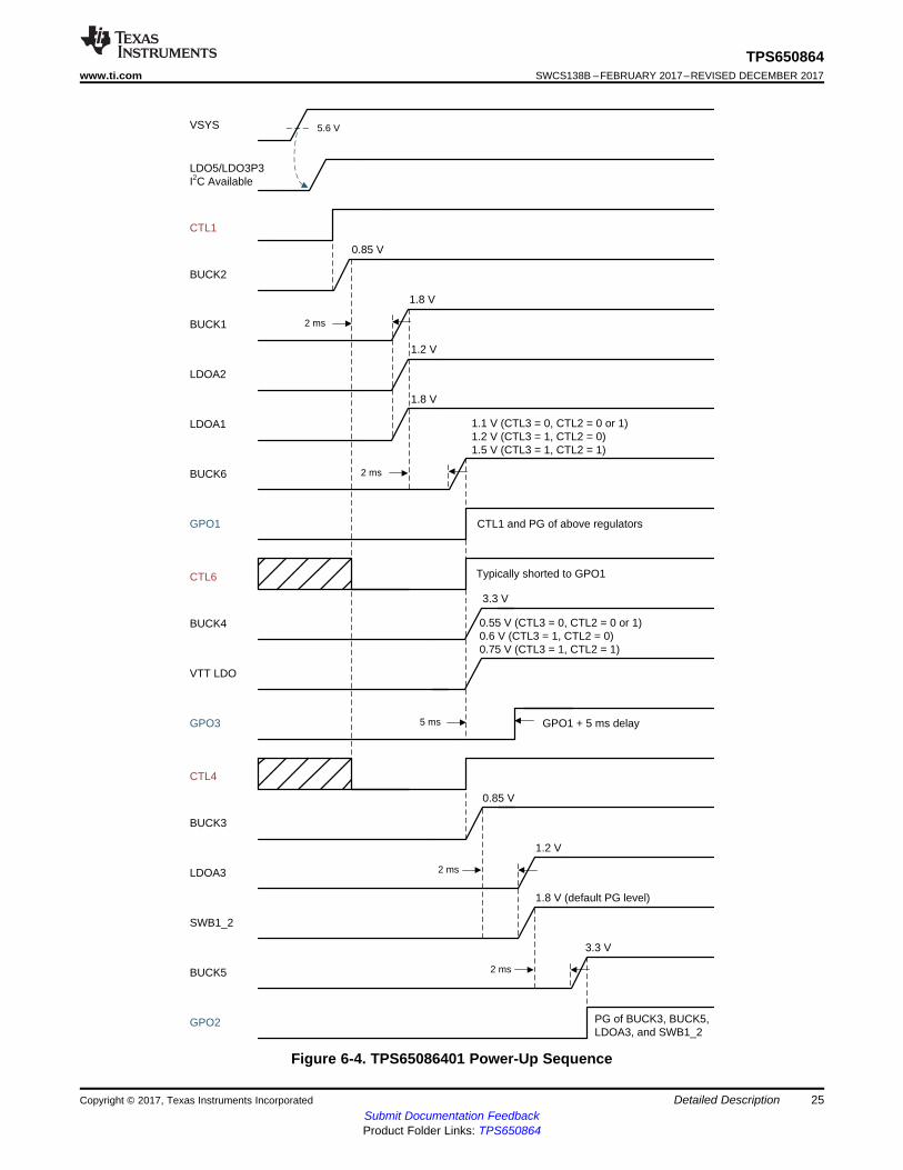
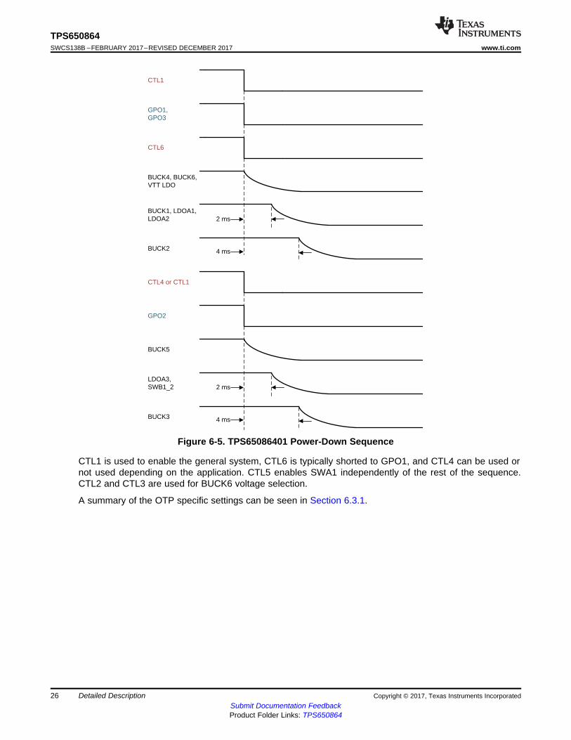
The power up and power down sequences can be seen in Figure 6-4 and Figure 6-5. Regulators andGPOs are enabled by combination of CTL pins and regulator power good signals.
CTL1
LDOA2
BUCK2
BUCK3
BUCK5
BUCK6
LDOA1
GPO1
BUCK1
BUCK4
VTT LDO
VSYS
LDO5/LDO3P3I2C Available
5.6 V
0.85 V
1.2 V
1.1 V (CTL3 = 0, CTL2 = 0 or 1)1.2 V (CTL3 = 1, CTL2 = 0)1.5 V (CTL3 = 1, CTL2 = 1)
1.8 V
1.8 V
3.3 V
0.85 V
3.3 V
CTL1 and PG of above regulators
2 ms
CTL6
2 ms
0.55 V (CTL3 = 0, CTL2 = 0 or 1)0.6 V (CTL3 = 1, CTL2 = 0)0.75 V (CTL3 = 1, CTL2 = 1)
CTL4
LDOA3
1.2 V
SWB1_2
1.8 V (default PG level)
GPO3 GPO1 + 5 ms delay5 ms
2 ms
2 ms
GPO2 PG of BUCK3, BUCK5,LDOA3, and SWB1_2
Typically shorted to GPO1
25
TPS650864www.ti.com SWCS138B –FEBRUARY 2017–REVISED DECEMBER 2017
Submit Documentation FeedbackProduct Folder Links: TPS650864
Detailed DescriptionCopyright © 2017, Texas Instruments Incorporated
Figure 6-4. TPS65086401 Power-Up Sequence
CTL1
BUCK2
BUCK4, BUCK6, VTT LDO
BUCK1, LDOA1,LDOA2
GPO1,GPO3
2 ms
4 ms
CTL4 or CTL1
BUCK3
BUCK5
LDOA3,SWB1_2
GPO2
2 ms
4 ms
CTL6
26
TPS650864SWCS138B –FEBRUARY 2017–REVISED DECEMBER 2017 www.ti.com
Submit Documentation FeedbackProduct Folder Links: TPS650864
Detailed Description Copyright © 2017, Texas Instruments Incorporated
Figure 6-5. TPS65086401 Power-Down Sequence
CTL1 is used to enable the general system, CTL6 is typically shorted to GPO1, and CTL4 can be used ornot used depending on the application. CTL5 enables SWA1 independently of the rest of the sequence.CTL2 and CTL3 are used for BUCK6 voltage selection.
A summary of the OTP specific settings can be seen in Section 6.3.1.
27
TPS650864www.ti.com SWCS138B –FEBRUARY 2017–REVISED DECEMBER 2017
Submit Documentation FeedbackProduct Folder Links: TPS650864
Detailed DescriptionCopyright © 2017, Texas Instruments Incorporated
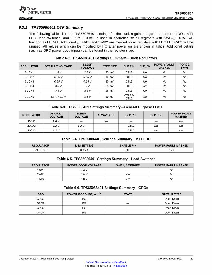
6.3.1 TPS65086401 OTP SummaryThe following tables list the TPS65086401 settings for the buck regulators, general purpose LDOs, VTTLDO, load switches, and GPOs. LDOA1 is used in sequence so all registers with SWB2_LDOA1 willfunction as LDOA1. Additionally, SWB1 and SWB2 are merged so all registers with LDOA1_SWB2 will beunused. All values which can be modified by I2C after power on are shown in italics. Additional details(such as GPO power good inputs) can be found in the register map.
Table 6-2. TPS65086401 Settings Summary—Buck Regulators
REGULATOR DEFAULT VOLTAGE SLEEPVOLTAGE STEP SIZE SLP PIN SLP_EN POWER FAULT
MASKEDFORCEPWM
BUCK1 1.8 V 1.8 V 25 mV CTL3 No No NoBUCK2 0.85 V 0.85 V 10 mV CTL3 No No NoBUCK3 0.85 V 0.85 V 25 mV CTL3 No No NoBUCK4 3.3 V 0 V 25 mV CTL6 Yes No NoBUCK5 3.3 V 3.3 V 25 mV CTL3 No No No
BUCK6 1.5 V / 1.2 V 1.1 V 10 mV CTL2 &CTL3 Yes No No
Table 6-3. TPS65086401 Settings Summary—General Purpose LDOs
REGULATOR DEFAULTVOLTAGE
SLEEPVOLTAGE ALWAYS ON SLP PIN SLP_EN POWER FAULT
MASKEDLDOA1 1.8 V — No — — NoLDOA2 1.2 V 1.2 V — CTL3 No NoLDOA3 1.2 V 1.2 V — CTL3 No No
Table 6-4. TPS65086401 Settings Summary—VTT LDO
REGULATOR ILIM SETTING ENABLE PIN POWER FAULT MASKEDVTT LDO 0.95 A CTL6 Yes
Table 6-5. TPS65086401 Settings Summary—Load Switches
REGULATOR POWER GOOD VOLTAGE SWB1_2 MERGED POWER FAULT MASKEDSWA1 3.3 V — NoSWB1 1.8 V Yes NoSWB2 1.8 V Yes No
Table 6-6. TPS65086401 Settings Summary—GPOs
GPO POWER GOOD (PG) or I2C STATE OUTPUT TYPEGPO1 PG — Open DrainGPO2 PG — Open DrainGPO3 PG — Open DrainGPO4 PG — Open Drain
BUCK1
BUCK2
BUCK3 3A
BUCK4 3A
BUCK5 3A
BUCK6
VTT LDO ±0.5A
LDOA2 0.6A
LDOA3 0.6A
SWA1 0.3A
SWB1 0.4A
SWB2 0.4A
LDOA1 0.2A
LDO5
CTL1 (Main Sequence)
IRQB
SCLK
DATA
EXT FET
EXT FET
EXT FET
VCCINT & VCCBRAM
VCC_AUX
VMGTAVTT
VCCOa
VCCOb
DDR3 / DDR3L
VDDQ
PMIC SoC
VIN
VIN
BUCK5V
VIN < 21 V
LDO5V
LDO5V1.0 V
VIN
VTT
VING1 up to 3.3V
VING2 up to 3.3V
1.8 V
1.2 V
1.35 V / 1.5 V
0.675 V / 0.75 V
1.8 V
0.7 V - 1.5 V
0.7 V - 1.5 V
VINLDO up to 2V
PLATFORM
VSUPP1
VSUPP2
VSUPP3
VSUPP4
VSUPP5
VSUPP6
2.5 V
3.3 V
CTL2 (Main Sequence)
CTL3 (VTT_EN)
CTL4 (SWA1_SWB1_EN)
CTL5 (SWB2_EN)
CTL6 (DDR_SEL)
GPO1 (BUCK1/2 PG)
GPO2 (System PG)
GPO3 (I2C controlled)
GPO4 (I2C controlled)PG_5V
+
REF±
Copyright © 2017, Texas Instruments Incorporated
28
TPS650864SWCS138B –FEBRUARY 2017–REVISED DECEMBER 2017 www.ti.com
Submit Documentation FeedbackProduct Folder Links: TPS650864
Detailed Description Copyright © 2017, Texas Instruments Incorporated
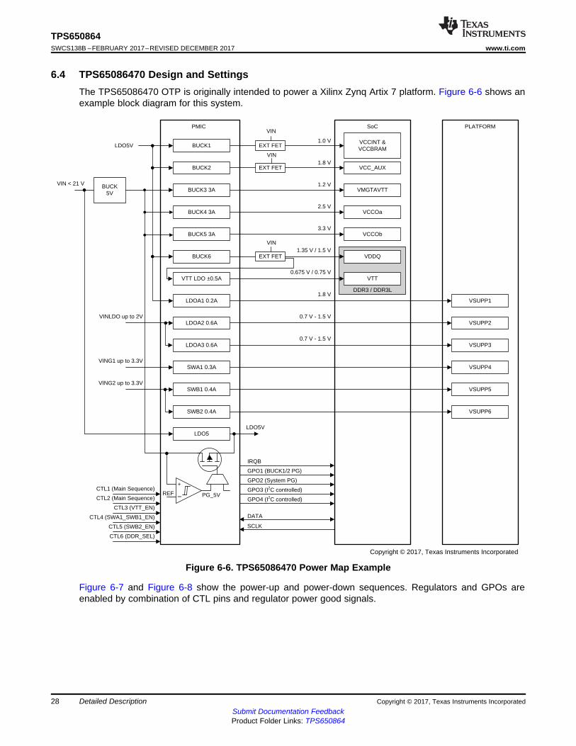
6.4 TPS65086470 Design and SettingsThe TPS65086470 OTP is originally intended to power a Xilinx Zynq Artix 7 platform. Figure 6-6 shows anexample block diagram for this system.
Figure 6-6. TPS65086470 Power Map Example
Figure 6-7 and Figure 6-8 show the power-up and power-down sequences. Regulators and GPOs areenabled by combination of CTL pins and regulator power good signals.

VSYS
LDO5/LDO3P3I2C Available
CTL1
BUCK1(VCC_INT)
BUCK2(VCC_AUX)
GPO1(BUCK1/2 PG)
BUCK3(VMGTAVTT)
BUCK4(VCCOa)
CTL2
BUCK5(VCCOb)
BUCK6 (VCCO_DDR)
GPO2(System PG)
VTT LDO
5.6 V
1.5 V if CTL6 = µ0¶1.35 V if CTL6 = µ1¶
1 V
1.8 V
1.2 V
2.5 V
3.3 V
Disabled if CTL3 = µ0¶0.75 V if CTL6 = µ0¶�& CTL3 = µ1¶0.675 V if CTL6 = µ1¶�& CTL3 = µ1¶
PG of all BUCKs + VTT LDO
2.5 ms
29
TPS650864www.ti.com SWCS138B –FEBRUARY 2017–REVISED DECEMBER 2017
Submit Documentation FeedbackProduct Folder Links: TPS650864
Detailed DescriptionCopyright © 2017, Texas Instruments Incorporated
Figure 6-7. TPS65086470 Power-Up Sequence
CTL2
GPO2(System PG)
BUCK6(VCCO_DDR)
BUCK5(VCCOb)
VTT LDO
BUCK4(VCCOa)
BUCK3(VMGTAVTT)
4 ms
CTL1
GPO1(BUCK1/2 PG)
BUCK2(VCC_AUX)
BUCK1(VCC_INT)
4 ms
30
TPS650864SWCS138B –FEBRUARY 2017–REVISED DECEMBER 2017 www.ti.com
Submit Documentation FeedbackProduct Folder Links: TPS650864
Detailed Description Copyright © 2017, Texas Instruments Incorporated
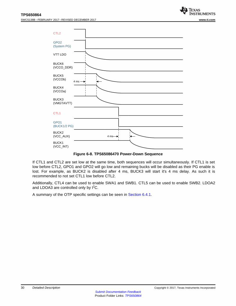
Figure 6-8. TPS65086470 Power-Down Sequence
If CTL1 and CTL2 are set low at the same time, both sequences will occur simultaneously. If CTL1 is setlow before CTL2, GPO1 and GPO2 will go low and remaining bucks will be disabled as their PG enable islost. For example, as BUCK2 is disabled after 4 ms, BUCK3 will start it's 4 ms delay. As such it isrecommended to not set CTL1 low before CTL2.
Additionally, CTL4 can be used to enable SWA1 and SWB1. CTL5 can be used to enable SWB2. LDOA2and LDOA3 are controlled only by I2C.
A summary of the OTP specific settings can be seen in Section 6.4.1.

31
TPS650864www.ti.com SWCS138B –FEBRUARY 2017–REVISED DECEMBER 2017
Submit Documentation FeedbackProduct Folder Links: TPS650864
Detailed DescriptionCopyright © 2017, Texas Instruments Incorporated
6.4.1 TPS65086470 OTP SummaryThe following tables list the TPS65086470 settings for the buck regulators (Table 6-7), general purposeLDOs (Table 6-8), VTT LDO (Table 6-9), load switches (Table 6-10), and GPOs (Table 6-11). LDOA1 isnot used in sequence so all registers with LDOA1_SWB2 will function as LDOA1. Additionally, SWB1 andSWB2 are not merged so all registers with SWB2_LDOA1 will function as SWB2. All values which can bemodified by I2C after power on are shown in italics. Additional details (such as GPO power good inputs)can be found in the register map.
Table 6-7. TPS65086470 Settings Summary—Buck Regulators
REGULATOR DEFAULT VOLTAGE SLEEPVOLTAGE STEP SIZE SLP PIN SLP_EN POWER FAULT
MASKEDFORCEPWM
BUCK1 1 V 1 V 10 mV CTL6 No No NoBUCK2 1.8 V 1.8 V 25 mV CTL6 No No NoBUCK3 1.2 V 1.2 V 25 mV CTL6 No No NoBUCK4 2.5 V 2.5 V 25 mV CTL6 No No NoBUCK5 3.3 V 3.3 V 25 mV CTL6 No No NoBUCK6 1.5 V 1.35 V 25 mV CTL6 Yes No No
Table 6-8. TPS65086470 Settings Summary—General Purpose LDOs
REGULATOR DEFAULTVOLTAGE
SLEEPVOLTAGE ALWAYS ON SLP PIN SLP_EN POWER FAULT
MASKEDLDOA1 1.8 V — No — — YesLDOA2 0.7 V 0.7 V — CTL6 No YesLDOA3 0.7 V 0.7 V — CTL6 No Yes
Table 6-9. TPS65086470 Settings Summary—VTT LDO
REGULATOR ILIM SETTING ENABLE PIN POWER FAULT MASKEDVTT LDO 0.95 A CTL3 No
Table 6-10. TPS65086470 Settings Summary—Load Switches
REGULATOR POWER GOOD VOLTAGE SWB1_2 MERGED POWER FAULT MASKEDSWA1 3.3 V — YesSWB1 1.8 V No YesSWB2 1.8 V No Yes
Table 6-11. TPS65086470 Settings Summary—GPOs
GPO POWER GOOD (PG) OR I2C STATE OUTPUT TYPEGPO1 PG — Open drainGPO2 PG — Open drainGPO3 I2C Low Open drainGPO4 I2C Low Open drain

32
TPS650864SWCS138B –FEBRUARY 2017–REVISED DECEMBER 2017 www.ti.com
Submit Documentation FeedbackProduct Folder Links: TPS650864
Detailed Description Copyright © 2017, Texas Instruments Incorporated
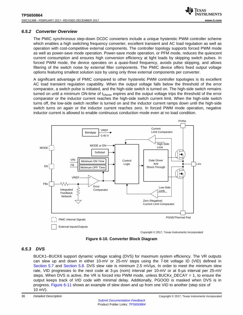
6.5 SMPS Voltage RegulatorsThe buck controllers integrate gate drivers for external power stages with programmable current limit (setby an external resistor at ILIMx pin), which allows for optimal selection of external passive componentsbased on the desired system load. The buck converters include integrated power stage and require aminimum number of pins for power input, inductor, and output voltage feedback input. Combined withhigh-frequency switching, all these features allow use of inductors in small form factor, thus reducing total-system cost and size.
BUCK1–BUCK6 have selectable auto- and forced-pulse width modulation (PWM) mode through theBUCKx_MODE bit in the BUCKxCTRL register. In default auto mode, the VR automatically switchesbetween PWM and pulsed frequency modulation (PFM) depending on the output load to maximizeefficiency.
All controllers and converters can be set to default VOUT or dynamically voltage changing at any time. Thismeans that the rails can be programmed for any VOUT by the factory, so the device starts up with thedefault voltage, or during operation the rail can be programmed to another operating VOUT while the rail isenable or disabled. There are two step sizes or ranges available for VOUT selection: 10-mV and 25-mVsteps. The step-size range must be selected prior to use and must be programmed by the factory. It is notsubject to programming or change during operation.
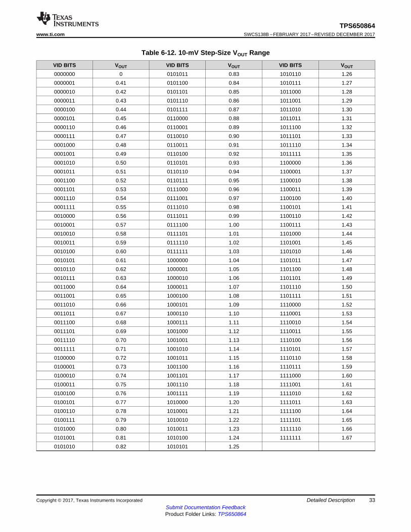
For the 10-mV step-size range VOUT options, see Table 6-12. For the 25-mV step-size range VOUT options,see Table 6-13.
33
TPS650864www.ti.com SWCS138B –FEBRUARY 2017–REVISED DECEMBER 2017
Submit Documentation FeedbackProduct Folder Links: TPS650864
Detailed DescriptionCopyright © 2017, Texas Instruments Incorporated
Table 6-12. 10-mV Step-Size VOUT Range
VID BITS VOUT VID BITS VOUT VID BITS VOUT
0000000 0 0101011 0.83 1010110 1.260000001 0.41 0101100 0.84 1010111 1.270000010 0.42 0101101 0.85 1011000 1.280000011 0.43 0101110 0.86 1011001 1.290000100 0.44 0101111 0.87 1011010 1.300000101 0.45 0110000 0.88 1011011 1.310000110 0.46 0110001 0.89 1011100 1.320000111 0.47 0110010 0.90 1011101 1.330001000 0.48 0110011 0.91 1011110 1.340001001 0.49 0110100 0.92 1011111 1.350001010 0.50 0110101 0.93 1100000 1.360001011 0.51 0110110 0.94 1100001 1.370001100 0.52 0110111 0.95 1100010 1.380001101 0.53 0111000 0.96 1100011 1.390001110 0.54 0111001 0.97 1100100 1.400001111 0.55 0111010 0.98 1100101 1.410010000 0.56 0111011 0.99 1100110 1.420010001 0.57 0111100 1.00 1100111 1.430010010 0.58 0111101 1.01 1101000 1.440010011 0.59 0111110 1.02 1101001 1.450010100 0.60 0111111 1.03 1101010 1.460010101 0.61 1000000 1.04 1101011 1.470010110 0.62 1000001 1.05 1101100 1.480010111 0.63 1000010 1.06 1101101 1.490011000 0.64 1000011 1.07 1101110 1.500011001 0.65 1000100 1.08 1101111 1.510011010 0.66 1000101 1.09 1110000 1.520011011 0.67 1000110 1.10 1110001 1.530011100 0.68 1000111 1.11 1110010 1.540011101 0.69 1001000 1.12 1110011 1.550011110 0.70 1001001 1.13 1110100 1.560011111 0.71 1001010 1.14 1110101 1.570100000 0.72 1001011 1.15 1110110 1.580100001 0.73 1001100 1.16 1110111 1.590100010 0.74 1001101 1.17 1111000 1.600100011 0.75 1001110 1.18 1111001 1.610100100 0.76 1001111 1.19 1111010 1.620100101 0.77 1010000 1.20 1111011 1.630100110 0.78 1010001 1.21 1111100 1.640100111 0.79 1010010 1.22 1111101 1.650101000 0.80 1010011 1.23 1111110 1.660101001 0.81 1010100 1.24 1111111 1.670101010 0.82 1010101 1.25

34
TPS650864SWCS138B –FEBRUARY 2017–REVISED DECEMBER 2017 www.ti.com
Submit Documentation FeedbackProduct Folder Links: TPS650864
Detailed Description Copyright © 2017, Texas Instruments Incorporated
Table 6-13. 25-mV Step-Size VOUT Range
VID BITS VOUT(Converters)
VOUT(Controllers) VID BITS VOUT VID BITS VOUT
0000000 0 0 0101011 1.475 1010110 2.5500000001 0.425 1.000 0101100 1.500 1010111 2.5750000010 0.450 1.000 0101101 1.525 1011000 2.6000000011 0.475 1.000 0101110 1.550 1011001 2.6250000100 0.500 1.000 0101111 1.575 1011010 2.6500000101 0.525 1.000 0110000 1.600 1011011 2.6750000110 0.550 1.000 0110001 1.625 1011100 2.7000000111 0.575 1.000 0110010 1.650 1011101 2.7250001000 0.600 1.000 0110011 1.675 1011110 2.7500001001 0.625 1.000 0110100 1.700 1011111 2.7750001010 0.650 1.000 0110101 1.725 1100000 2.8000001011 0.675 1.000 0110110 1.750 1100001 2.8250001100 0.700 1.000 0110111 1.775 1100010 2.8500001101 0.725 1.000 0111000 1.800 1100011 2.8750001110 0.750 1.000 0111001 1.825 1100100 2.9000001111 0.775 1.000 0111010 1.850 1100101 2.9250010000 0.800 1.000 0111011 1.875 1100110 2.9500010001 0.825 1.000 0111100 1.900 1100111 2.9750010010 0.850 1.000 0111101 1.925 1101000 3.0000010011 0.875 1.000 0111110 1.950 1101001 3.0250010100 0.900 1.000 0111111 1.975 1101010 3.0500010101 0.925 1.000 1000000 2.000 1101011 3.0750010110 0.950 1.000 1000001 2.025 1101100 3.1000010111 0.975 1.000 1000010 2.050 1101101 3.1250011000 1.000 1.000 1000011 2.075 1101110 3.1500011001 1.025 1.025 1000100 2.100 1101111 3.1750011010 1.050 1.050 1000101 2.125 1110000 3.2000011011 1.075 1.075 1000110 2.150 1110001 3.2250011100 1.100 1.100 1000111 2.175 1110010 3.2500011101 1.125 1.125 1001000 2.200 1110011 3.2750011110 1.150 1.150 1001001 2.225 1110100 3.3000011111 1.175 1.175 1001010 2.250 1110101 3.3250100000 1.200 1.200 1001011 2.275 1110110 3.3500100001 1.225 1.225 1001100 2.300 1110111 3.3750100010 1.250 1.250 1001101 2.325 1111000 3.4000100011 1.275 1.275 1001110 2.350 1111001 3.4250100100 1.300 1.300 1001111 2.375 1111010 3.4500100101 1.325 1.325 1010000 2.400 1111011 3.4750100110 1.350 1.350 1010001 2.425 1111100 3.5000100111 1.375 1.375 1010010 2.450 1111101 3.5250101000 1.400 1.400 1010011 2.475 1111110 3.5500101001 1.425 1.425 1010100 2.500 1111111 3.5750101010 1.450 1.450 1010101 2.525
+
PGOOD
DCHG
SWx
NOC
ZC
XCON
DRVLx
PWM
Control Logic
+
+
UV
VSYS
GND
REF
One-Shot
50 µA
BOOTx
DRVHx
FAULT
PGOOD
ILIM
+
VFB
OC+
+
SS Ramp Comp
EN
VDD
HS
LS
DRV5V_x_x
PGNDSNSx
VREF ± VTH_PG
++
Ramp Generator
PMIC Internal Signals External Inputs/Outputs
±
±
±
±
VREF + VTH_PG
±
+
±
OV+
±
Copyright © 2017, Texas Instruments Incorporated
35
TPS650864www.ti.com SWCS138B –FEBRUARY 2017–REVISED DECEMBER 2017
Submit Documentation FeedbackProduct Folder Links: TPS650864
Detailed DescriptionCopyright © 2017, Texas Instruments Incorporated
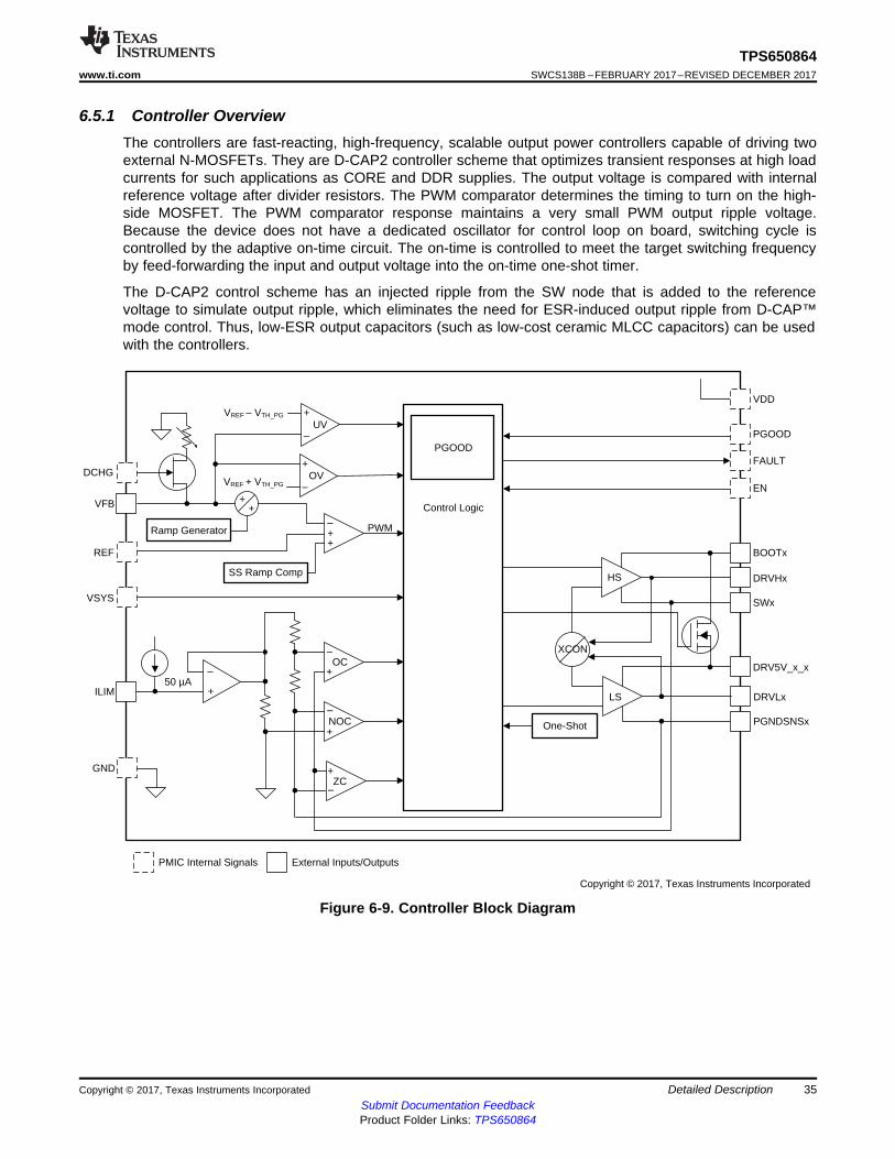
6.5.1 Controller OverviewThe controllers are fast-reacting, high-frequency, scalable output power controllers capable of driving twoexternal N-MOSFETs. They are D-CAP2 controller scheme that optimizes transient responses at high loadcurrents for such applications as CORE and DDR supplies. The output voltage is compared with internalreference voltage after divider resistors. The PWM comparator determines the timing to turn on the high-side MOSFET. The PWM comparator response maintains a very small PWM output ripple voltage.Because the device does not have a dedicated oscillator for control loop on board, switching cycle iscontrolled by the adaptive on-time circuit. The on-time is controlled to meet the target switching frequencyby feed-forwarding the input and output voltage into the on-time one-shot timer.
The D-CAP2 control scheme has an injected ripple from the SW node that is added to the referencevoltage to simulate output ripple, which eliminates the need for ESR-induced output ripple from D-CAP™mode control. Thus, low-ESR output capacitors (such as low-cost ceramic MLCC capacitors) can be usedwith the controllers.
Figure 6-9. Controller Block Diagram
Bandgap
Minimum ON Time
Minimum OFF Time
Gate DriverAnti
Shoot-Through
CurrentLimit Comparator
LXx
FBx
EN
MODE
PVINx
PGND/Thermal Pad
VIN
VREF
FB
ErrorComparator
Zero (Negative)Current Limit Comparator
ControlLogic
MODE or EN
VREF
0.40 V
Softstart
PMIC Internal Signals
External Inputs/Outputs
IntegratedFeedbackNetwork
High-SideLimit
+
±
Low-SideLimit
Copyright © 2017, Texas Instruments Incorporated
36
TPS650864SWCS138B –FEBRUARY 2017–REVISED DECEMBER 2017 www.ti.com
Submit Documentation FeedbackProduct Folder Links: TPS650864
Detailed Description Copyright © 2017, Texas Instruments Incorporated
6.5.2 Converter OverviewThe PMIC synchronous step-down DCDC converters include a unique hysteretic PWM controller schemewhich enables a high switching frequency converter, excellent transient and AC load regulation as well asoperation with cost-competitive external components. The controller topology supports forced PWM modeas well as power-save mode operation. Power-save mode operation, or PFM mode, reduces the quiescentcurrent consumption and ensures high conversion efficiency at light loads by skipping switch pulses. Inforced PWM mode, the device operates on a quasi-fixed frequency, avoids pulse skipping, and allowsfiltering of the switch noise by external filter components. The PMIC device offers fixed output voltageoptions featuring smallest solution size by using only three external components per converter.
A significant advantage of PMIC compared to other hysteretic PWM controller topologies is its excellentAC load transient regulation capability. When the output voltage falls below the threshold of the errorcomparator, a switch pulse is initiated, and the high-side switch is turned on. The high-side switch remainsturned on until a minimum ON-time of tONmin expires and the output voltage trips the threshold of the errorcomparator or the inductor current reaches the high-side switch current limit. When the high-side switchturns off, the low-side switch rectifier is turned on and the inductor current ramps down until the high-sideswitch turns on again or the inductor current reaches zero. In forced PWM mode operation, negativeinductor current is allowed to enable continuous conduction mode even at no load condition.
Figure 6-10. Converter Block Diagram
6.5.3 DVSBUCK1–BUCK6 support dynamic voltage scaling (DVS) for maximum system efficiency. The VR outputscan slew up and down in either 10-mV or 25-mV steps using the 7-bit voltage ID (VID) defined inSection 5.7 and Section 5.8. DVS slew rate is minimum 2.5 mV/µs. In order to meet the minimum slewrate, VID progresses to the next code at 3-µs (nom) interval per 10-mV or at 6-µs interval per 25-mVsteps. When DVS is active, the VR is forced into PWM mode, unless BUCKx_DECAY = 1, to ensure theoutput keeps track of VID code with minimal delay. Additionally, PGOOD is masked when DVS is inprogress. Figure 6-11 shows an example of slew down and up from one VID to another (step size of10 mV).

VID
Number of Steps × 3 µsVOUT
200 µsLoad and Time Dependent
VID
Number of Steps × 3 µs
VOUT
37
TPS650864www.ti.com SWCS138B –FEBRUARY 2017–REVISED DECEMBER 2017
Submit Documentation FeedbackProduct Folder Links: TPS650864
Detailed DescriptionCopyright © 2017, Texas Instruments Incorporated
Figure 6-11. DVS Timing Diagram I (BUCKx_DECAY = 0)
As shown in Figure 6-12, if a BUCKx_VID[6:0] is set to 7b000 0000, its output voltage will slew down to0.5 V first, and then will drift down to 0 V as the SMPS stops switching. Subsequently, if aBUCKx_VID[6:0] is set to a value (neither 7b000 0000 nor 7b000 0001) when its output voltage is lessthan 0.5 V, the VR will ramp up to 0.5 V first with soft-start kicking in, then will slew up to target voltage inthe slew rate aforementioned. It must be noted that a fixed 200 µs of soft-start time is reserved for VOUT toreach 0.5 V. In this case, however, the SMPS is not forced into PWM mode as it otherwise could causeVOUT to droop momentarily if VOUT might have been drifting above 0.5 V for any reason.
Figure 6-12. DVS Timing Diagram II (BUCKx_DECAY = 0)
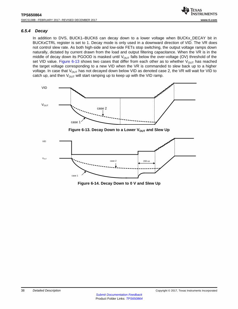
VID
VOUT
case 2
case 1
200 us
VID
VOUT
case 2
case 1
38
TPS650864SWCS138B –FEBRUARY 2017–REVISED DECEMBER 2017 www.ti.com
Submit Documentation FeedbackProduct Folder Links: TPS650864
Detailed Description Copyright © 2017, Texas Instruments Incorporated
6.5.4 DecayIn addition to DVS, BUCK1–BUCK6 can decay down to a lower voltage when BUCKx_DECAY bit inBUCKxCTRL register is set to 1. Decay mode is only used in a downward direction of VID. The VR doesnot control slew rate. As both high-side and low-side FETs stop switching, the output voltage ramps downnaturally, dictated by current drawn from the load and output filtering capacitance. When the VR is in themiddle of decay down its PGOOD is masked until VOUT falls below the over-voltage (OV) threshold of theset VID value. Figure 6-13 shows two cases that differ from each other as to whether VOUT has reachedthe target voltage corresponding to a new VID when the VR is commanded to slew back up to a highervoltage. In case that VOUT has not decayed down below VID as denoted case 2, the VR will wait for VID tocatch up, and then VOUT will start ramping up to keep up with the VID ramp.
Figure 6-13. Decay Down to a Lower VOUT and Slew Up
Figure 6-14. Decay Down to 0 V and Slew Up
OUT IN(MIN) OUTripple(min)
max IN(MIN) sw(max)
V (V V )I
L V f
�
u u
ripple(min)DSON LIM
ILIMLIMREF
IR 8 1.3 I
2R
I
§ ·u u u �¨ ¸
© ¹
39
TPS650864www.ti.com SWCS138B –FEBRUARY 2017–REVISED DECEMBER 2017
Submit Documentation FeedbackProduct Folder Links: TPS650864
Detailed DescriptionCopyright © 2017, Texas Instruments Incorporated
6.5.5 Current LimitThe buck controllers (BUCK1, BUCK2, and BUCK6) have inductor-valley current-limit architecture and thecurrent limit is programmable by an external resistor at the ILIMx pin. Equation 1 shows the calculation fora desired resistor value, depending on specific application conditions. ILIMREF is the current source out ofthe ILIMx pin that is typically 50 µA, and RDSON is the maximum channel resistance of the low-side FET.The scaling factor is 1.3 to take into account all errors and temperature variations of RDSON, ILIMREF, andRILIM. Finally, 8 is another scaling factor associated with ILIMREF.
where• ILIM is the target current limit. An appropriate margin must be allowed when determining ILIM from
maximum output DC load current.• Iripple(min) is the minimum peak-to-peak inductor ripple current for a given VOUT. (1)
where• Lmax is maximum inductance• fsw(max) is maximum switching frequency• VIN(MIN) minimum input voltage to the external power stage (2)
The buck converter limit inductor peak current cycle-by-cycle to IIND_LIM is specified in Section 5.8.
6.6 LDOs and Load Switches
6.6.1 VTT LDOTypically powered from the BUCK6 output, the VTT LDO tracks FBVOUT6 and regulates it's output toFBVOUT6 / 2. The LDO current limit is OTP dependent, and it is designed specifically to power DDRmemory. The LDO core is a transconductance amplifier with large gain, and it drives a current outputstage that either sources or sinks current depending on the deviation of the VTTFB pin voltage from thetarget regulation voltage.
6.6.2 LDOA1–LDOA3The TPS650864xx device integrates three general purpose LDOs. LDOA1 is powered from a 5-V supplythrough the DRV5V_2_A1 pin and it can be factory configured to be an Always-On rail (stay on even incase of emergency shutdown) as long as a valid power supply is available at VSYS. See Table 6-14 forLDOA1 output voltage options. LDOA2 and LDOA3 share a power input pin (PVINLDOA2_A3). The outputregulation voltages are set by writing to LDOAx_VID[3:0] bits (Reg 0x9A, 0x9B, and 0xAE). See Table 6-15 for LDOA2 and LDOA3 output voltage options. LDOA1 is controlled by the LDOA1_SWB2_CTRLregister.
Table 6-14. LDOA1 Output Voltage Options
VID BITS VOUT VID BITS VOUT VID BITS VOUT VID BITS VOUT
0000 1.35 0100 1.8 1000 2.3 1100 2.850001 1.5 0101 1.9 1001 2.4 1101 3.00010 1.6 0110 2.0 1010 2.5 1110 3.30011 1.7 0111 2.1 1011 2.6 1111 Not Used

40
TPS650864SWCS138B –FEBRUARY 2017–REVISED DECEMBER 2017 www.ti.com
Submit Documentation FeedbackProduct Folder Links: TPS650864
Detailed Description Copyright © 2017, Texas Instruments Incorporated
Table 6-15. LDOA2 and LDOA3 Output Voltage Options
VID BITS VOUT VID BITS VOUT VID BITS VOUT VID BITS VOUT
0000 0.70 0100 0.90 1000 1.10 1100 1.300001 0.75 0101 0.95 1001 1.15 1101 1.350010 0.80 0110 1.00 1010 1.20 1110 1.400011 0.85 0111 1.05 1011 1.25 1111 1.50
6.6.3 Load SwitchesThe PMIC features three general-purpose load switches. SWA1 has its own power input pin (PVINSWA1),while SWB1 and SWB2 share one power input pin (PVINSWB1_B2). All switches have built-in slew ratecontrol during start-up to limit the inrush current.
6.7 Power Goods (PGOOD or PG) and GPOsThe device provides information on status of VRs through four GPO pins along with Power Good Statusregisters defined in Section 6.11.50 and Section 6.11.51. Power Good information of any individual VRand load switch can be assigned to be part of the PGOOD tree as defined from Section 6.11.40 toSection 6.11.47. PGOOD assertion delays are programmable from 0 ms to 15 ms for GPO1, 5 ms to 100ms for GPO3, and 0 ms to 100 ms for GPO2 and GPO4, respectively, as are defined in Section 6.11.21and Section 6.11.34.

BUCK1_PG
BUCK1_MSK (bit)
BUCK2_PG
BUCK2_MSK (bit)
BUCK3_PG
BUCK3_MSK (bit)
BUCK4_PG
BUCK4_MSK (bit)
BUCK5_PG
BUCK5_MSK (bit)
BUCK6_PG
BUCK6_MSK (bit)
SWA1_PG
SWA1_MSK (bit)
LDOA2_PG
LDOA2_MSK (bit)
LDOA3_PG
LDOA3_MSK (bit)
SWB1_PG
SWB1_MSK (bit)
SWB2_LDOA1_PG
SWB2_LDOA1_MSK (bit)
VTT_PG
VTT_MSK (bit)
CTL1
CTL2
CTL2_MSK (bit)
CTL3/SLPENB1
CTL3_MSK (bit)
CTL4
CTL4_MSK (bit)
CTL5
CTL5_MSK (bit)
SelectableRisingEdgeDelay
GPO_PG
CTL6/SLPENB2
CTL6_MSK (bit)
CTL1_MSK (bit)
41
TPS650864www.ti.com SWCS138B –FEBRUARY 2017–REVISED DECEMBER 2017
Submit Documentation FeedbackProduct Folder Links: TPS650864
Detailed DescriptionCopyright © 2017, Texas Instruments Incorporated
Figure 6-15. Power Good Tree
Alternatively, the GPOs can be used as general purpose outputs controlled by the user through I2C. Referto the Section 6.11.37 for details on controlling the GPOs in I2C control mode.

42
TPS650864SWCS138B –FEBRUARY 2017–REVISED DECEMBER 2017 www.ti.com
Submit Documentation FeedbackProduct Folder Links: TPS650864
Detailed Description Copyright © 2017, Texas Instruments Incorporated
6.8 Power Sequencing and VR ControlThe device has three different ways of sequencing the rails during power up and power down:• Rail enabled by CTLx pin• Rail enabled by Power Good (PG) of previously enabled rail• Rail enabled by I2C software command
A delay can be added from any CTLx pin or PG to the enable of the subjected enabled rail. This creates avery flexible device capable of many sequence options. If a rail cannot be sequenced automatically, anyrail can be enabled or disabled through an I2C command.
6.8.1 CTLx SequencingThe device has six control-input pins (CTL1–CTL6) to control six SMPS regulators, three LDO regulators,and three load switches. This allows the user to define up to six distinctive groups, to which each VR canbe assigned for highly flexible power sequencing. Of the six CTLx pins, CTL3 and CTL6 can be configuredalternatively to active-low sleep enable pins. For instance, if a system level SLEEP state is defined suchthat BUCK1 output regulation voltage is lower than in the normal mode, then BUCK1 SLEEP state can beassigned to CTL3 or CTL6. By being pulled low, either CTL3 or CTL6 can be used to put BUCK1 intoSLEEP state, and BUCK1 will regulate its output at a voltage defined by BUCK1_SLP_VID[6:0] inSection 6.11.23. For a demonstration of this feature, Figure 6-16 shows how BUCK1 is enabled from theCTL1 pin.
6.8.2 PG SequencingAny rail can be sequenced by the Power Good of a prior rail. This can be combined with the CTLx methodto allow for further sequence control and create more distinctive groups of enables than the six from CTLx.This also allows some of the CTLx pins to be freed up for other purposes such as logic input gates. For ademonstration of this feature, Figure 6-16 shows how the BUCK5 is enabled from the BUCK4 PG.

VSYS
LDO5/LDO3P3LDOA1/GPO1I2C Available
CTL1
BUCK1
BUCK2
2 ms
BUCK6
4 ms
BUCK3
BUCK4
CTL2
BUCK5
GPO4
CTL5
SWA1
LDOA2
CTL4
SWB2
5.6 V
LDOA3
GPO3
SWB1
16 ms
PG of all BUCKs
PG of BUCKs and LDOs
CTL6
VTT
2 ms
8 ms
43
TPS650864www.ti.com SWCS138B –FEBRUARY 2017–REVISED DECEMBER 2017
Submit Documentation FeedbackProduct Folder Links: TPS650864
Detailed DescriptionCopyright © 2017, Texas Instruments Incorporated
Figure 6-16. Generic Power-Up Sequence Example
6.8.3 Enable DelayA delay can be added to the enable of any rail after the desired CTLx and PGs are met. This allows forthe option to create additional timing groups from either CTLx pins or internal PGs. For a demonstration ofthis feature, Figure 6-16 shows how BUCK2 and BUCK6 are enabled after BUCK1 is enabled from CTL1pin.
44
TPS650864SWCS138B –FEBRUARY 2017–REVISED DECEMBER 2017 www.ti.com
Submit Documentation FeedbackProduct Folder Links: TPS650864
Detailed Description Copyright © 2017, Texas Instruments Incorporated
6.8.4 Power-Up SequenceWhen a valid power supply is detected at the VSYS pin as VSYS crosses above VSYS_UVLO_5V +VSYS_UVLO+5V_HYS, the power-up sequence is initiated by driving one of the control input pins high, followedby the rest of pins in order. Figure 6-16 is an example where CTL1–CTL4 are defined to control fourgroups of VRs, while GPO3 and GPO4 are defined to provide a PGOOD status of two groups. The controlinput pins do not necessarily have to be pulled up in a staggered manner. For instance, if CTL2 is pulledup from the preceding group of VRs before PGOOD has been asserted at GPO1, the BUCK4 enable willbe delayed until the PGOOD is asserted.
For the specific sequencing of a TPS650864xx device, see Table 3-1.
6.8.5 Power-Down SequenceThe power-down sequence can follow the CTLx pins, or be controlled with the I2C commands. If theinternal PGs are used for sequencing or if some rails need to ramp down before others a delay can beadded to the deassertion low of the internal enable of the subjected rail. This delay can be independent ofthe power-up delay option. Thus, power-up and power-down sequences can be different or similar tomatch the specific application sequences required.
Refer to Figure 6-17 for an example of a power-down sequence demonstrating the delay disable ofBUCK1 and BUCK2.
For the specific sequencing of a TPS650864xx device, see Table 3-1.

CTL6
2 ms
VTT
SWA1
CTL5
CTL2
CTL1
BUCK6
BUCK2
BUCK1
4 ms
SWB1
SWB2
CTL4
LDOA2
LDOA3
BUCK6
BUCK5
BUCK4
GPO3
GPO4
45
TPS650864www.ti.com SWCS138B –FEBRUARY 2017–REVISED DECEMBER 2017
Submit Documentation FeedbackProduct Folder Links: TPS650864
Detailed DescriptionCopyright © 2017, Texas Instruments Incorporated
Figure 6-17. Generic Power-Down Sequence Example

VSYS
GPOx
BUCKx
LDOAx
SWx
VTT
444 ns (nominal with ± 1 ± % variation)
5.4 V
Normal State
CTL6
BUCK1
GPO1-GPO4
Sleep StateNormal State
CTL1-CTL4
1.8V
1.8 V
BUCK1_VID
BUCK1_SLP_VID
BUCK1_VID
1.8 V
0 V
BUCK1_DECAY = 1
BUCK1_DECAY = 0
46
TPS650864SWCS138B –FEBRUARY 2017–REVISED DECEMBER 2017 www.ti.com
Submit Documentation FeedbackProduct Folder Links: TPS650864
Detailed Description Copyright © 2017, Texas Instruments Incorporated
6.8.6 Sleep State Entry and Exit
Figure 6-18. Sleep State Entry and Exit Sequence Example
Figure 6-18 shows an example where BUCK1 is defined to enter Sleep State in response to CTL6 goinglow.
NOTEAll PGOODs from GPO1–GPO4 can stay asserted during the entry and the exit. Dependingon status of the BUCK1_DECAY bit defined in the BUCK1CTRL register, BUCK1 output willeither decay or slew down to a new voltage defined in BUCK1_SLP_VID[6:0].
6.8.7 Emergency Shutdown
Figure 6-19. Emergency Shutdown Sequence
When VSYS crosses below VSYS_UVLO_5V, all Power Good pins will be deasserted, and after 444 ns (nom) ofdelay all VRs will shut down. Upon shutdown, all internal discharge resistors are set to 100 Ω to ensuretimely decay of all VR outputs. Other conditions that will cause emergency shutdown are the dietemperature rising above the critical temperature threshold (TCRIT), deassertion of Power Good of any rail(configurable), or failure of any rail to reach power good within 10 ms of being enabled (configurable). IfPMIC was shutdown by UVLO, it will wait until VSYS rises above VSYS_UVLO_5V + VSYS_UVLO_5V_HYS beforereloading the default OTP and checking the state of the CTLx pins. If PMIC was shutdown by temperature,it will wait until temperature drops below TCRIT – TCRIT_HYS before reloading OTP and checking the state ofthe CTLx pins. If the PMIC was shutdown by power fault, it will reload OTP after disabling all rails andcheck the state of the CTLx pins once OTP has finished reloading.

47
TPS650864www.ti.com SWCS138B –FEBRUARY 2017–REVISED DECEMBER 2017
Submit Documentation FeedbackProduct Folder Links: TPS650864
Detailed DescriptionCopyright © 2017, Texas Instruments Incorporated
6.9 Device Functional Modes
6.9.1 Off ModeWhen power supply at the VSYS pin is less than VSYS_UVLO_5V (5.4-V nominal) + VSYS_UVLO_5V_HYS (0.2-Vnominal), the device is in off mode, where all output rails are disabled. If the supply voltage is greater thanVSYS_UVLO_3V (3.6-V nominal) + VSYS_UVLO_3V_HYS (0.15-V nominal) while it is still less than VSYS_UVLO_5V +VSYS_UVLO_5V_HYS, then the internal band-gap reference (VREF pin) along with LDO3P3 are enabled andregulated at target values.
6.9.2 Standby ModeWhen power supply at the VSYS pin rises above VSYS_UVLO_5V + VSYS_UVLO_5V_HYS, the device entersstandby mode, where all internal reference and regulators (LDO3P3 and LDO5) are up and running, andI2C interface and CTL pins are ready to respond. All default registers defined in Section 6.11 should haveby now been loaded from one-time programmable (OTP) memory. Quiescent current consumption instandby mode is specified in Section 5.5.
6.9.3 Active ModeThe device proceeds to active mode when any output rail is enabled either via an input pin as discussedin Section 6.8 or by writing to EN bits through I2C. Output regulation voltage can also be changed bywriting to VID bits defined in Section 6.11.
6.10 I2C InterfaceThe I2C interface is a 2-wire serial interface developed by NXP™ (formerly Philips Semiconductor) (seeI2C-Bus Specification and user manual, Rev 4, 13 February 2012). The bus consists of a data line (SDA)and a clock line (SCL) with pullup structures. When the bus is idle, both SDA and SCL lines are pulledhigh. All the I2C compatible devices connect to the I2C bus through open drain I/O pins, DATA and CLK. Amaster device, usually a microcontroller or a digital signal processor, controls the bus. The master isresponsible for generating the SCL signal and device addresses. The master also generates specificconditions that indicate the START and STOP of data transfer. A slave device receives and/or transmitsdata on the bus under control of the master device.
The TPS650864xx device works as a slave and supports the following data transfer modes, as defined inthe I2C-Bus Specification: standard mode (100 kbps), fast mode (400 kbps), and high-speed mode(1 Mbps). The interface adds flexibility to the power supply solution, enabling most functions to beprogrammed to new values depending on the instantaneous application requirements. Register contentsare loaded when VSYS higher than VSYS_UVLO_5V is applied to the TPS650864xx device. The I2C interface isrunning from an internal oscillator that is automatically enabled when there is an access to the interface.
The data transfer protocol for standard and fast modes are exactly the same, therefore, they are referredto as F/S-mode in this document. The protocol for high-speed mode is different from the F/S-mode, and itis referred to as H/S-mode.
The TPS650864xx device supports 7-bit addressing; however, 10-bit addressing and general call addressare not supported. The default device address is 0x5E.

SDA
SCL
Data Valid
Change of Data Allowed
SDA
SCL
S P
START Condition
STOPCondition
48
TPS650864SWCS138B –FEBRUARY 2017–REVISED DECEMBER 2017 www.ti.com
Submit Documentation FeedbackProduct Folder Links: TPS650864
Detailed Description Copyright © 2017, Texas Instruments Incorporated
6.10.1 F/S-Mode ProtocolThe master initiates data transfer by generating a start condition. The start condition is when a high-to-lowtransition occurs on the SDA line while SCL is high (see Figure 6-20). All I2C-compatible devices shouldrecognize a start condition.
The master then generates the SCL pulses, and transmits the 7-bit address and the read/write direction bitR/W on the SDA line. During all transmissions, the master ensures that data is valid. A valid datacondition requires the SDA line to be stable during the entire high period of the clock pulse (seeFigure 6-21). All devices recognize the address sent by the master and compare it to their internal fixedaddresses. Only the slave device with a matching address generates an acknowledge (see Figure 6-22),by pulling the SDA line low during the entire high period of the ninth SCL cycle. Upon detecting thisacknowledge, the master knows that the communication link with a slave has been established.
The master generates further SCL cycles to either transmit data to the slave (R/W bit = 0) or receive datafrom the slave (R/W bit = 1). In either case, the receiver needs to acknowledge the data sent by thetransmitter. An acknowledge signal can either be generated by the master or by the slave, depending onwhich one is the receiver. 9-bit valid data sequences consisting of 8-bit data and 1-bit acknowledge cancontinue as long as necessary.
To signal the end of the data transfer, the master generates a stop condition by pulling the SDA line fromlow to high while the SCL line is high (see Figure 6-20). This releases the bus and stops thecommunication link with the addressed slave. All I2C-compatible devices must recognize the stopcondition. Upon the receipt of a stop condition, all devices know that the bus is released, and they wait fora start condition followed by a matching address.
Figure 6-20. START and STOP Conditions
Figure 6-21. Bit Transfer on the I2C Bus

MSB
SDA
ACK Signal From Slave
Generate ACK Signal
SCL1 2 7 8 9 1 2 3-8 9
Address
ACK ACK
Byte Complete, Interrupt Within Slave
Clock Line Held Low While Interrupts Are ServicedS or Sr
START or Repeated START Condition
P or Sr
STOP or Repeated START Condition
R/W
Data Output at Transmitter
Data Output at Receiver
SCL from Master 1 2 8 9
S
START Condition
Not ACK
ACK
Clock pulse for ACK
49
TPS650864www.ti.com SWCS138B –FEBRUARY 2017–REVISED DECEMBER 2017
Submit Documentation FeedbackProduct Folder Links: TPS650864
Detailed DescriptionCopyright © 2017, Texas Instruments Incorporated
Figure 6-22. Acknowledge on the I2C Bus
Figure 6-23. I2C Bus Protocol
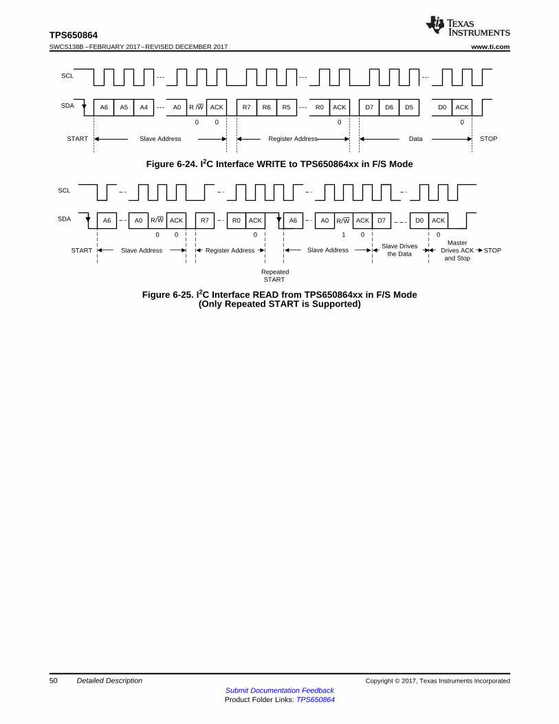
ACKA0 R7 R0 ACK A6 A0 ACK D7 D0 ACKA6
SCL
SDA
Slave Address Register Address Slave AddressSlave Drives
the Data
Master Drives ACK
and StopSTOPSTART
Repeated START
0 0 0 010
WR/WR/
A6 A5 A4 A0 ACK R7 R6 R5 R0 ACK D7 D6 D5 D0 ACK
SCL
SDA
Slave Address
0 0 0 0
Register Address DataSTART STOP
R /W
50
TPS650864SWCS138B –FEBRUARY 2017–REVISED DECEMBER 2017 www.ti.com
Submit Documentation FeedbackProduct Folder Links: TPS650864
Detailed Description Copyright © 2017, Texas Instruments Incorporated
Figure 6-24. I2C Interface WRITE to TPS650864xx in F/S Mode
Figure 6-25. I2C Interface READ from TPS650864xx in F/S Mode(Only Repeated START is Supported)
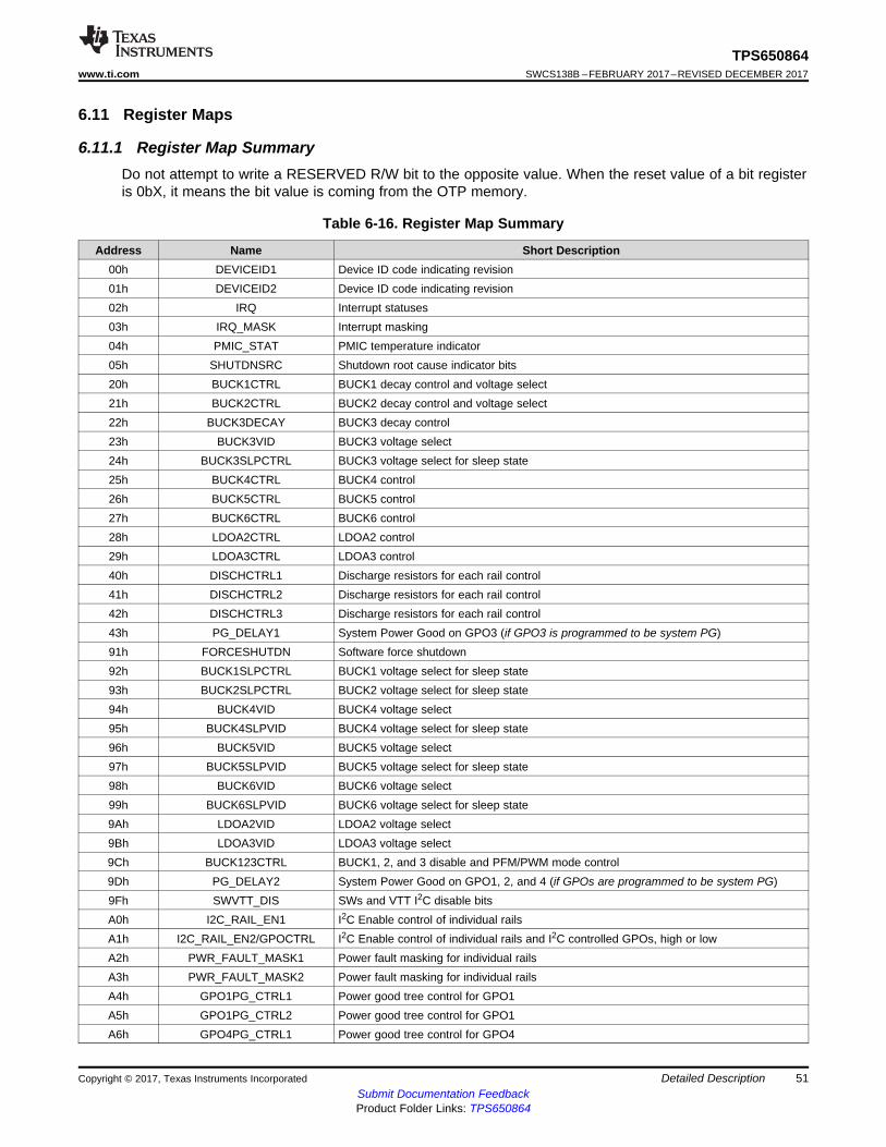
51
TPS650864www.ti.com SWCS138B –FEBRUARY 2017–REVISED DECEMBER 2017
Submit Documentation FeedbackProduct Folder Links: TPS650864
Detailed DescriptionCopyright © 2017, Texas Instruments Incorporated
6.11 Register Maps
6.11.1 Register Map SummaryDo not attempt to write a RESERVED R/W bit to the opposite value. When the reset value of a bit registeris 0bX, it means the bit value is coming from the OTP memory.
Table 6-16. Register Map Summary
Address Name Short Description00h DEVICEID1 Device ID code indicating revision01h DEVICEID2 Device ID code indicating revision02h IRQ Interrupt statuses03h IRQ_MASK Interrupt masking04h PMIC_STAT PMIC temperature indicator05h SHUTDNSRC Shutdown root cause indicator bits20h BUCK1CTRL BUCK1 decay control and voltage select21h BUCK2CTRL BUCK2 decay control and voltage select22h BUCK3DECAY BUCK3 decay control23h BUCK3VID BUCK3 voltage select24h BUCK3SLPCTRL BUCK3 voltage select for sleep state25h BUCK4CTRL BUCK4 control26h BUCK5CTRL BUCK5 control27h BUCK6CTRL BUCK6 control28h LDOA2CTRL LDOA2 control29h LDOA3CTRL LDOA3 control40h DISCHCTRL1 Discharge resistors for each rail control41h DISCHCTRL2 Discharge resistors for each rail control42h DISCHCTRL3 Discharge resistors for each rail control43h PG_DELAY1 System Power Good on GPO3 (if GPO3 is programmed to be system PG)91h FORCESHUTDN Software force shutdown92h BUCK1SLPCTRL BUCK1 voltage select for sleep state93h BUCK2SLPCTRL BUCK2 voltage select for sleep state94h BUCK4VID BUCK4 voltage select95h BUCK4SLPVID BUCK4 voltage select for sleep state96h BUCK5VID BUCK5 voltage select97h BUCK5SLPVID BUCK5 voltage select for sleep state98h BUCK6VID BUCK6 voltage select99h BUCK6SLPVID BUCK6 voltage select for sleep state9Ah LDOA2VID LDOA2 voltage select9Bh LDOA3VID LDOA3 voltage select9Ch BUCK123CTRL BUCK1, 2, and 3 disable and PFM/PWM mode control9Dh PG_DELAY2 System Power Good on GPO1, 2, and 4 (if GPOs are programmed to be system PG)9Fh SWVTT_DIS SWs and VTT I2C disable bitsA0h I2C_RAIL_EN1 I2C Enable control of individual railsA1h I2C_RAIL_EN2/GPOCTRL I2C Enable control of individual rails and I2C controlled GPOs, high or lowA2h PWR_FAULT_MASK1 Power fault masking for individual railsA3h PWR_FAULT_MASK2 Power fault masking for individual railsA4h GPO1PG_CTRL1 Power good tree control for GPO1A5h GPO1PG_CTRL2 Power good tree control for GPO1A6h GPO4PG_CTRL1 Power good tree control for GPO4

52
TPS650864SWCS138B –FEBRUARY 2017–REVISED DECEMBER 2017 www.ti.com
Submit Documentation FeedbackProduct Folder Links: TPS650864
Detailed Description Copyright © 2017, Texas Instruments Incorporated
Table 6-16. Register Map Summary (continued)Address Name Short Description
A7h GPO4PG_CTRL2 Power good tree control for GPO4A8h GPO2PG_CTRL1 Power good tree control for GPO2A9h GPO2PG_CTRL2 Power good tree control for GPO2AAh GPO3PG_CTRL1 Power good tree control for GPO3ABh GPO3PG_CTRL2 Power good tree control for GPO3ACh MISCSYSPG Power good tree control with CTL3 and CTL6 for GPOADh VTT_DISCH_CTRL Discharge resistor setting for VTT LDOAEh LDOA1_SWB2_CTRL LDOA1 and SWB2 control for discharge, voltage selection, and enableB0h PG_STATUS1 Power good statuses for individual railsB1h PG_STATUS2 Power good statuses for individual railsB2h PWR_FAULT_STATUS1 Power fault statuses for individual railsB3h PWR_FAULT_STATUS2 Power fault statuses for individual railsB4h TEMPCRIT Critical temperature indicatorsB5h TEMPHOT Hot temperature indicators
Complex bit access types are encoded to fit into small table cells. Table 6-17 shows the codes that areused for access types in this section.
Table 6-17. Access Type Codes
Access Type Code DescriptionRead TypeR R ReadWrite TypeW W Write
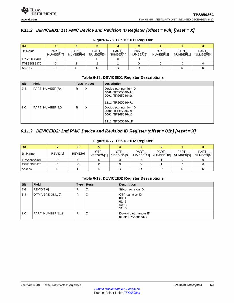
53
TPS650864www.ti.com SWCS138B –FEBRUARY 2017–REVISED DECEMBER 2017
Submit Documentation FeedbackProduct Folder Links: TPS650864
Detailed DescriptionCopyright © 2017, Texas Instruments Incorporated
6.11.2 DEVICEID1: 1st PMIC Device and Revision ID Register (offset = 00h) [reset = X]
Figure 6-26. DEVICEID1 RegisterBit 7 6 5 4 3 2 1 0Bit Name PART_
NUMBER[7]PART_
NUMBER[6]PART_
NUMBER[5]PART_
NUMBER[4]PART_
NUMBER[3]PART_
NUMBER[2]PART_
NUMBER[1]PART_
NUMBER[0]TPS65086401 0 0 0 0 0 0 0 1TPS65086470 0 1 1 1 0 0 0 0Access R R R R R R R R
Table 6-18. DEVICEID1 Register DescriptionsBit Field Type Reset Description7:4 PART_NUMBER[7:4] R X Device part number ID
0000: TPS65086x0x0001: TPS65086x1x...1111: TPS65086xFx
3:0 PART_NUMBER[3:0] R X Device part number ID0000: TPS65086xx00001: TPS65086xx1...1111: TPS65086xxF
6.11.3 DEVICEID2: 2nd PMIC Device and Revision ID Register (offset = 01h) [reset = X]
Figure 6-27. DEVICEID2 RegisterBit 7 6 5 4 3 2 1 0
Bit Name REVID[1] REVID[0] OTP_VERSION[1]
OTP_VERSION[0]
PART_NUMBER[11]
PART_NUMBER[10]
PART_NUMBER[9]
PART_NUMBER[8]
TPS65086401 0 0 0 0 0 1 0 0TPS65086470 0 0 0 0 0 1 0 0Access R R R R R R R R
Table 6-19. DEVICEID2 Register DescriptionsBit Field Type Reset Description7:6 REVID[1:0] R X Silicon revision ID5:4 OTP_VERSION[1:0] R X OTP variation ID
00: A01: B10: C11: D
3:0 PART_NUMBER[11:8] R X Device part number ID0100: TPS650864xx

54
TPS650864SWCS138B –FEBRUARY 2017–REVISED DECEMBER 2017 www.ti.com
Submit Documentation FeedbackProduct Folder Links: TPS650864
Detailed Description Copyright © 2017, Texas Instruments Incorporated
6.11.4 IRQ: PMIC Interrupt Register (offset = 02h) [reset = 0000 0000]
Figure 6-28. IRQ RegisterBit 7 6 5 4 3 2 1 0Bit Name FAULT RESERVED RESERVED RESERVED SHUTDN RESERVED RESERVED DIETEMPTPS650864xx 0 0 0 0 0 0 0 0Access R/W R R R R/W R R R/W
Table 6-20. IRQ Register DescriptionsBit Field Type Reset Description7 FAULT R/W 0 Fault interrupt. Asserted when either condition occurs: power fault of any rail, or
die temperature crosses over the critical temperature threshold (TCRIT). Theuser can read Reg. 0xB2–0xB6 to determine what has caused the interrupt.0: Not asserted1: Asserted. Host to write 1 to clear.
3 SHUTDN R/W 0 Asserted when PMIC shuts down. To clear indicator, SHUTDNSRC must becleared first, see Section 6.11.70: Not asserted.1: Asserted. Host to write 1 to clear.
0 DIETEMP R/W 0 Die temp interrupt. Asserted when PMIC die temperature crosses above the hottemperature threshold (THOT).0: Not asserted.1: Asserted. Host to write 1 to clear.
6.11.5 IRQ_MASK: PMIC Interrupt Mask Register (offset = 03h) [reset = 1111 1111]
Figure 6-29. IRQ_MASK RegisterBit 7 6 5 4 3 2 1 0Bit Name MFAULT RESERVED RESERVED RESERVED MSHUTDN RESERVED RESERVED MDIETEMPTPS650864xx 1 1 1 1 1 1 1 1Access R/W R R R R/W R R R/W
Table 6-21. IRQ_MASK Register DescriptionsBit Field Type Reset Description7 MFAULT R/W 1 FAULT interrupt mask.
0: Not masked.1: Masked.
3 MSHUTDN R/W 1 PMIC shutdown event interrupt mask0: Not masked.1: Masked.
0 MDIETEMP R/W 1 Die temp interrupt mask.0: Not masked.1: Masked.
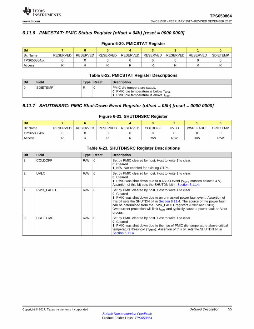
55
TPS650864www.ti.com SWCS138B –FEBRUARY 2017–REVISED DECEMBER 2017
Submit Documentation FeedbackProduct Folder Links: TPS650864
Detailed DescriptionCopyright © 2017, Texas Instruments Incorporated
6.11.6 PMICSTAT: PMIC Status Register (offset = 04h) [reset = 0000 0000]
Figure 6-30. PMICSTAT RegisterBit 7 6 5 4 3 2 1 0Bit Name RESERVED RESERVED RESERVED RESERVED RESERVED RESERVED RESERVED SDIETEMPTPS650864xx 0 0 0 0 0 0 0 0Access R R R R R R R R
Table 6-22. PMICSTAT Register DescriptionsBit Field Type Reset Description0 SDIETEMP R 0 PMIC die temperature status.
0: PMIC die temperature is below THOT.1: PMIC die temperature is above THOT.
6.11.7 SHUTDNSRC: PMIC Shut-Down Event Register (offset = 05h) [reset = 0000 0000]
Figure 6-31. SHUTDNSRC RegisterBit 7 6 5 4 3 2 1 0Bit Name RESERVED RESERVED RESERVED RESERVED COLDOFF UVLO PWR_FAULT CRITTEMPTPS650864xx 0 0 0 0 0 0 0 0Access R R R R R/W R/W R/W R/W
Table 6-23. SHUTDNSRC Register DescriptionsBit Field Type Reset Description3 COLDOFF R/W 0 Set by PMIC cleared by host. Host to write 1 to clear.
0: Cleared1: N/A. Not enabled for existing OTPs.
2 UVLO R/W 0 Set by PMIC cleared by host. Host to write 1 to clear.0: Cleared1: PMIC was shut down due to a UVLO event (VSYS crosses below 5.4 V).Assertion of this bit sets the SHUTDN bit in Section 6.11.4.
1 PWR_FAULT R/W 0 Set by PMIC cleared by host. Host to write 1 to clear.0: Cleared1: PMIC was shut down due to an unmasked power fault event. Assertion ofthis bit sets the SHUTDN bit in Section 6.11.4. The source of the power faultcan be determined from the PWR_FAULT registers (0xB2 and 0xB3).Overcurrent protection will limit IOUT and typically cause a power fault as Voutdroops.
0 CRITTEMP R/W 0 Set by PMIC cleared by host. Host to write 1 to clear.0: Cleared1: PMIC was shut down due to the rise of PMIC die temperature above criticaltemperature threshold (TCRIT). Assertion of this bit sets the SHUTDN bit inSection 6.11.4.

56
TPS650864SWCS138B –FEBRUARY 2017–REVISED DECEMBER 2017 www.ti.com
Submit Documentation FeedbackProduct Folder Links: TPS650864
Detailed Description Copyright © 2017, Texas Instruments Incorporated
6.11.8 BUCK1CTRL: BUCK1 Control Register (offset = 20h) [reset = X]
Figure 6-32. BUCK1CTRL RegisterBit 7 6 5 4 3 2 1 0
Bit Name BUCK1_VID[6]
BUCK1_VID[5]
BUCK1_VID[4]
BUCK1_VID[3]
BUCK1_VID[2]
BUCK1_VID[1]
BUCK1_VID[0]
BUCK1_DECAY
TPS65086401 0 1 1 1 0 0 0 0TPS65086470 0 1 1 1 1 0 0 0Access R/W R/W R/W R/W R/W R/W R/W R/W
Table 6-24. BUCK1CTRL Register DescriptionsBit Field Type Reset Description7:1 BUCK1_VID[6:0] R/W X This field sets the BUCK1 regulator output regulation voltage in
normal mode.See Table 6-12 and Table 6-13 for 10-mV and 25-mV step rangesfor VOUT options.
0 BUCK1_DECAY R/W X Decay Bit0: The output slews down to a lower voltage set by the VID bits.1: The output decays down to a lower voltage set by the VID bits.Decay rate depends on total capacitance and load present at theoutput.
6.11.9 BUCK2CTRL: BUCK2 Control Register (offset = 21h) [reset = X]
Figure 6-33. BUCK2CTRL RegisterBit 7 6 5 4 3 2 1 0
Bit Name BUCK2_VID[6]
BUCK2_VID[5]
BUCK2_VID[4]
BUCK2_VID[3]
BUCK2_VID[2]
BUCK2_VID[1]
BUCK2_VID[0]
BUCK2_DECAY
TPS65086401 0 1 0 1 1 0 1 0TPS65086470 0 1 1 1 0 0 0 0Access R/W R/W R/W R/W R/W R/W R/W R/W
Table 6-25. BUCK2CTRL Register DescriptionsBit Field Type Reset Description7:1 BUCK2_VID[6:0] R/W X This field sets the BUCK2 regulator output regulation voltage in
normal mode.See Table 6-12 and Table 6-13 for 10-mV and 25-mV step rangesfor VOUT options.
0 BUCK2_DECAY R/W X Decay Bit0: The output slews down to a lower voltage set by the VID bits.1: The output decays down to a lower voltage set by the VID bits.Decay rate depends on total capacitance and load present at theoutput.

57
TPS650864www.ti.com SWCS138B –FEBRUARY 2017–REVISED DECEMBER 2017
Submit Documentation FeedbackProduct Folder Links: TPS650864
Detailed DescriptionCopyright © 2017, Texas Instruments Incorporated
6.11.10 BUCK3DECAY: BUCK3 Decay Control Register (offset = 22h) [reset = X]
Figure 6-34. BUCK3DECAY RegisterBit 7 6 5 4 3 2 1 0
Bit Name SPARE SPARE SPARE SPARE SPARE SPARE SPARE BUCK3_DECAY
TPS65086401 0 0 1 0 0 1 0 0TPS65086470 0 1 0 0 0 0 0 0Access R/W R/W R/W R/W R/W R/W R/W R/W
Table 6-26. BUCK3DECAY Register DescriptionsBit Field Type Reset Description7:1 SPARE R/W X Unused. Typically mirror BUCK3_VID by default in OTP.0 BUCK3_DECAY R/W X Decay Bit
0: The output slews down to a lower voltage set by the VID bits.1: The output decays down to a lower voltage set by the VID bits.Decay rate depends on total capacitance and load present at theoutput.
6.11.11 BUCK3VID: BUCK3 VID Register (offset = 23h) [reset = X]
Figure 6-35. BUCK3VID RegisterBit 7 6 5 4 3 2 1 0
Bit Name BUCK3_VID[6]
BUCK3_VID[5]
BUCK3_VID[4]
BUCK3_VID[3]
BUCK3_VID[2]
BUCK3_VID[1]
BUCK3_VID[0] RESERVED
TPS65086401 0 0 1 0 0 1 0 0TPS65086470 0 1 0 0 0 0 0 0Access R/W R/W R/W R/W R/W R/W R/W R
Table 6-27. BUCK3VID Register DescriptionsBit Field Type Reset Description7:1 BUCK3_VID[6:0] R/W X This field sets the BUCK3 regulator output regulation voltage in
normal mode.See Table 6-12 and Table 6-13 for 10-mV and 25-mV step rangesfor VOUT options.
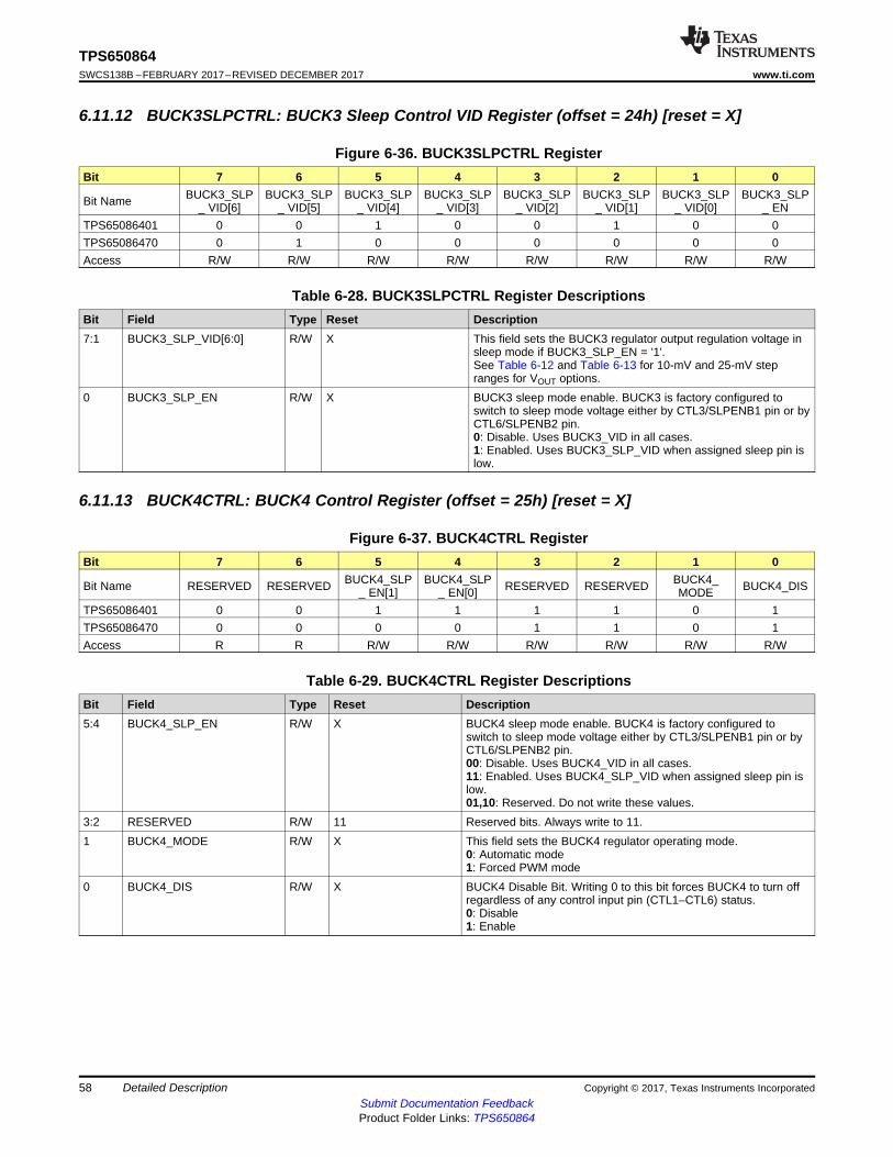
58
TPS650864SWCS138B –FEBRUARY 2017–REVISED DECEMBER 2017 www.ti.com
Submit Documentation FeedbackProduct Folder Links: TPS650864
Detailed Description Copyright © 2017, Texas Instruments Incorporated
6.11.12 BUCK3SLPCTRL: BUCK3 Sleep Control VID Register (offset = 24h) [reset = X]
Figure 6-36. BUCK3SLPCTRL RegisterBit 7 6 5 4 3 2 1 0
Bit Name BUCK3_SLP_ VID[6]
BUCK3_SLP_ VID[5]
BUCK3_SLP_ VID[4]
BUCK3_SLP_ VID[3]
BUCK3_SLP_ VID[2]
BUCK3_SLP_ VID[1]
BUCK3_SLP_ VID[0]
BUCK3_SLP_ EN
TPS65086401 0 0 1 0 0 1 0 0TPS65086470 0 1 0 0 0 0 0 0Access R/W R/W R/W R/W R/W R/W R/W R/W
Table 6-28. BUCK3SLPCTRL Register DescriptionsBit Field Type Reset Description7:1 BUCK3_SLP_VID[6:0] R/W X This field sets the BUCK3 regulator output regulation voltage in
sleep mode if BUCK3_SLP_EN = '1'.See Table 6-12 and Table 6-13 for 10-mV and 25-mV stepranges for VOUT options.
0 BUCK3_SLP_EN R/W X BUCK3 sleep mode enable. BUCK3 is factory configured toswitch to sleep mode voltage either by CTL3/SLPENB1 pin or byCTL6/SLPENB2 pin.0: Disable. Uses BUCK3_VID in all cases.1: Enabled. Uses BUCK3_SLP_VID when assigned sleep pin islow.
6.11.13 BUCK4CTRL: BUCK4 Control Register (offset = 25h) [reset = X]
Figure 6-37. BUCK4CTRL RegisterBit 7 6 5 4 3 2 1 0
Bit Name RESERVED RESERVED BUCK4_SLP_ EN[1]
BUCK4_SLP_ EN[0] RESERVED RESERVED BUCK4_
MODE BUCK4_DIS
TPS65086401 0 0 1 1 1 1 0 1TPS65086470 0 0 0 0 1 1 0 1Access R R R/W R/W R/W R/W R/W R/W
Table 6-29. BUCK4CTRL Register DescriptionsBit Field Type Reset Description5:4 BUCK4_SLP_EN R/W X BUCK4 sleep mode enable. BUCK4 is factory configured to
switch to sleep mode voltage either by CTL3/SLPENB1 pin or byCTL6/SLPENB2 pin.00: Disable. Uses BUCK4_VID in all cases.11: Enabled. Uses BUCK4_SLP_VID when assigned sleep pin islow.01,10: Reserved. Do not write these values.
3:2 RESERVED R/W 11 Reserved bits. Always write to 11.1 BUCK4_MODE R/W X This field sets the BUCK4 regulator operating mode.
0: Automatic mode1: Forced PWM mode
0 BUCK4_DIS R/W X BUCK4 Disable Bit. Writing 0 to this bit forces BUCK4 to turn offregardless of any control input pin (CTL1–CTL6) status.0: Disable1: Enable
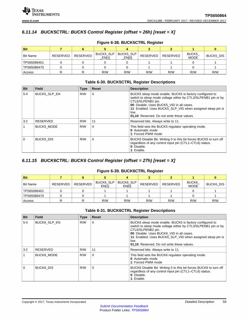
59
TPS650864www.ti.com SWCS138B –FEBRUARY 2017–REVISED DECEMBER 2017
Submit Documentation FeedbackProduct Folder Links: TPS650864
Detailed DescriptionCopyright © 2017, Texas Instruments Incorporated
6.11.14 BUCK5CTRL: BUCK5 Control Register (offset = 26h) [reset = X]
Figure 6-38. BUCK5CTRL RegisterBit 7 6 5 4 3 2 1 0
Bit Name RESERVED RESERVED BUCK5_SLP_EN[1]
BUCK5_SLP_EN[0] RESERVED RESERVED BUCK5_
MODE BUCK5_DIS
TPS65086401 0 0 0 0 1 1 0 1TPS65086470 0 0 0 0 1 1 0 1Access R R R/W R/W R/W R/W R/W R/W
Table 6-30. BUCK5CTRL Register DescriptionsBit Field Type Reset Description5:4 BUCK5_SLP_EN R/W X BUCK5 sleep mode enable. BUCK5 is factory configured to
switch to sleep mode voltage either by CTL3/SLPENB1 pin or byCTL6/SLPENB2 pin.00: Disable. Uses BUCK5_VID in all cases.11: Enabled. Uses BUCK5_SLP_VID when assigned sleep pin islow.01,10: Reserved. Do not write these values.
3:2 RESERVED R/W 11 Reserved bits. Always write to 11.1 BUCK5_MODE R/W X This field sets the BUCK5 regulator operating mode.
0: Automatic mode1: Forced PWM mode
0 BUCK5_DIS R/W X BUCK5 Disable Bit. Writing 0 to this bit forces BUCK5 to turn offregardless of any control input pin (CTL1–CTL6) status.0: Disable.1: Enable.
6.11.15 BUCK6CTRL: BUCK6 Control Register (offset = 27h) [reset = X]
Figure 6-39. BUCK6CTRL RegisterBit 7 6 5 4 3 2 1 0
Bit Name RESERVED RESERVED BUCK6_SLPEN[1]
BUCK6_SLPEN[0] RESERVED RESERVED BUCK6_
MODE BUCK6_DIS
TPS65086401 0 0 1 1 1 1 0 1TPS65086470 0 0 1 1 1 1 0 1Access R R R/W R/W R/W R/W R/W R/W
Table 6-31. BUCK6CTRL Register DescriptionsBit Field Type Reset Description5:4 BUCK6_SLP_EN R/W X BUCK6 sleep mode enable. BUCK6 is factory configured to
switch to sleep mode voltage either by CTL3/SLPENB1 pin or byCTL6/SLPENB2 pin.00: Disable. Uses BUCK6_VID in all cases.11: Enabled. Uses BUCK6_SLP_VID when assigned sleep pin islow.01,10: Reserved. Do not write these values.
3:2 RESERVED R/W 11 Reserved bits. Always write to 11.1 BUCK6_MODE R/W X This field sets the BUCK6 regulator operating mode.
0: Automatic mode1: Forced PWM mode
0 BUCK6_DIS R/W X BUCK6 Disable Bit. Writing 0 to this bit forces BUCK6 to turn offregardless of any control input pin (CTL1–CTL6) status.0: Disable.1: Enable.
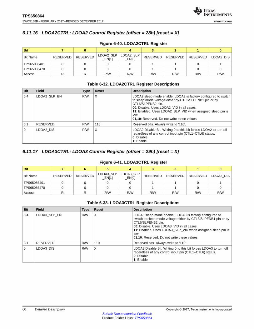
60
TPS650864SWCS138B –FEBRUARY 2017–REVISED DECEMBER 2017 www.ti.com
Submit Documentation FeedbackProduct Folder Links: TPS650864
Detailed Description Copyright © 2017, Texas Instruments Incorporated
6.11.16 LDOA2CTRL: LDOA2 Control Register (offset = 28h) [reset = X]
Figure 6-40. LDOA2CTRL RegisterBit 7 6 5 4 3 2 1 0
Bit Name RESERVED RESERVED LDOA2_SLP_EN[1]
LDOA2_SLP_EN[0] RESERVED RESERVED RESERVED LDOA2_DIS
TPS65086401 0 0 0 0 1 1 0 1TPS65086470 0 0 0 0 1 1 0 0Access R R R/W R/W R/W R/W R/W R/W
Table 6-32. LDOA2CTRL Register DescriptionsBit Field Type Reset Description5:4 LDOA2_SLP_EN R/W X LDOA2 sleep mode enable. LDOA2 is factory configured to switch
to sleep mode voltage either by CTL3/SLPENB1 pin or byCTL6/SLPENB2 pin.00: Disable. Uses LDOA2_VID in all cases.11: Enabled. Uses LDOA2_SLP_VID when assigned sleep pin islow.01,10: Reserved. Do not write these values.
3:1 RESERVED R/W 110 Reserved bits. Always write to '110'.0 LDOA2_DIS R/W X LDOA2 Disable Bit. Writing 0 to this bit forces LDOA2 to turn off
regardless of any control input pin (CTL1–CTL6) status.0: Disable.1: Enable.
6.11.17 LDOA3CTRL: LDOA3 Control Register (offset = 29h) [reset = X]
Figure 6-41. LDOA3CTRL RegisterBit 7 6 5 4 3 2 1 0
Bit Name RESERVED RESERVED LDOA3_SLP_EN[1]
LDOA3_SLP_EN[0] RESERVED RESERVED RESERVED LDOA3_DIS
TPS65086401 0 0 0 0 1 1 0 1TPS65086470 0 0 0 0 1 1 0 0Access R R R/W R/W R/W R/W R/W R/W
Table 6-33. LDOA3CTRL Register DescriptionsBit Field Type Reset Description5:4 LDOA3_SLP_EN R/W X LDOA3 sleep mode enable. LDOA3 is factory configured to
switch to sleep mode voltage either by CTL3/SLPENB1 pin or byCTL6/SLPENB2 pin.00: Disable. Uses LDOA3_VID in all cases.11: Enabled. Uses LDOA3_SLP_VID when assigned sleep pin islow.01,10: Reserved. Do not write these values.
3:1 RESERVED R/W 110 Reserved bits. Always write to '110'.0 LDOA3_DIS R/W X LDOA3 Disable Bit. Writing 0 to this bit forces LDOA3 to turn off
regardless of any control input pin (CTL1–CTL6) status.0: Disable1: Enable

61
TPS650864www.ti.com SWCS138B –FEBRUARY 2017–REVISED DECEMBER 2017
Submit Documentation FeedbackProduct Folder Links: TPS650864
Detailed DescriptionCopyright © 2017, Texas Instruments Incorporated
6.11.18 DISCHCTRL1: 1st Discharge Control Register (offset = 40h) [reset = X]All xx_DISCHG[1:0] bits internally set to 00 whenever the corresponding VR is enabled.
Figure 6-42. DISCHCTRL1 RegisterBit 7 6 5 4 3 2 1 0
Bit Name BUCK4_DISCHG[1]
BUCK4_DISCHG[0]
BUCK3_DISCHG[1]
BUCK3_DISCHG[0]
BUCK2_DISCHG[1]
BUCK2_DISCHG[0]
BUCK1_DISCHG[1]
BUCK1_DISCHG[0]
TPS65086401 0 1 0 1 0 1 0 1TPS65086470 0 1 0 1 0 1 0 1Access R/W R/W R/W R/W R/W R/W R/W R/W
Table 6-34. DISCHCTRL1 Register DescriptionsBit Field Type Reset Description7:6 BUCK4_DISCHG[1:0] R/W X BUCK4 discharge resistance
00: no discharge01: 100 Ω10: 200 Ω11: 500 Ω
5:4 BUCK3_DISCHG[1:0] R/W X BUCK3 discharge resistance00: no discharge01: 100 Ω10: 200 Ω11: 500 Ω
3:2 BUCK2_DISCHG[1:0] R/W X BUCK2 discharge resistance00: no discharge01: 100 Ω10: 200 Ω11: 500 Ω
1:0 BUCK1_DISCHG[1:0] R/W X BUCK1 discharge resistance00: no discharge01: 100 Ω10: 200 Ω11: 500 Ω

62
TPS650864SWCS138B –FEBRUARY 2017–REVISED DECEMBER 2017 www.ti.com
Submit Documentation FeedbackProduct Folder Links: TPS650864
Detailed Description Copyright © 2017, Texas Instruments Incorporated
6.11.19 DISCHCTRL2: 2nd Discharge Control Register (offset = 41h) [reset = X]All xx_DISCHG[1:0] bits internally set to 00 whenever the corresponding VR is enabled.
Figure 6-43. DISCHCTRL2 RegisterBit 7 6 5 4 3 2 1 0
Bit Name LDOA2_DISCHG[1]
LDOA2_DISCHG[0]
SWA1_DISCHG[1]
SWA1_DISCHG[0]
BUCK6_DISCHG[1]
BUCK6_DISCHG[0]
BUCK5_DISCHG[1]
BUCK5_DISCHG[0]
TPS65086401 0 1 0 1 0 1 0 1TPS65086470 0 1 0 0 0 1 0 1Access R/W R/W R/W R/W R/W R/W R/W R/W
Table 6-35. DISCHCTRL2 Register DescriptionsBit Field Type Reset Description7:6 LDOA2_DISCHG[1:0] R/W X LDOA2 discharge resistance
00: no discharge01: 100 Ω10: 200 Ω11: 500 Ω
5:4 SWA1_DISCHG[1:0] R/W X SWA1 discharge resistance00: no discharge01: 100 Ω10: 200 Ω11: 500 Ω
3:2 BUCK6_DISCHG[1:0] R/W X BUCK6 discharge resistance00: no discharge01: 100 Ω10: 200 Ω11: 500 Ω
1:0 BUCK5_DISCHG[1:0] R/W X BUCK5 discharge resistance00: no discharge01: 100 Ω10: 200 Ω11: 500 Ω

63
TPS650864www.ti.com SWCS138B –FEBRUARY 2017–REVISED DECEMBER 2017
Submit Documentation FeedbackProduct Folder Links: TPS650864
Detailed DescriptionCopyright © 2017, Texas Instruments Incorporated
6.11.20 DISCHCTRL3: 3rd Discharge Control Register (offset = 42h) [reset = X]All xx_DISCHG[1:0] bits internally set to 00 whenever the corresponding VR is enabled.
Figure 6-44. DISCHCTRL3 RegisterBit 7 6 5 4 3 2 1 0
Bit Name RESERVED RESERVED SWB2_DISCHG[1]
SWB2_DISCHG[0]
SWB1_DISCHG[1]
SWB1_DISCHG[0]
LDOA3_DISCHG[1]
LDOA3_DISCHG[0]
TPS65086401 0 0 0 1 0 1 0 1TPS65086470 0 0 0 0 0 0 0 1Access R R R/W R/W R/W R/W R/W R/W
Table 6-36. DISCHCTRL3 Register DescriptionsBit Field Type Reset Description5:4 SWB2_DISCHG[1:0] R/W X SWB2 discharge resistance
00: no discharge01: 100 Ω10: 200 Ω11: 500 Ω
3:2 SWB1_DISCHG[1:0] R/W X SWB1 discharge resistance00: no discharge01: 100 Ω10: 200 Ω11: 500 Ω
1:0 LDOA3_DISCHG[1:0] R/W X LDOA3 discharge resistance00: no discharge01: 100 Ω10: 200 Ω11: 500 Ω
6.11.21 PG_DELAY1: 1st Power Good Delay Register (offset = 43h) [reset = X]Programmable Power Good delay for GPO3 pin, measured from the moment when all VRs assigned toGPO3 pin reach their regulation range to Power Good assertion. This is an optional register as the PMICcan be programmed for system PG, level shifter or I2C controller GPO.
Figure 6-45. PG_DELAY1 RegisterBit 7 6 5 4 3 2 1 0
Bit Name RESERVED RESERVED RESERVED RESERVED RESERVED GPO3_PG_DELAY[2]
GPO3_PG_DELAY[1]
GPO3_PG_DELAY[0]
TPS65086401 0 0 0 0 0 0 0 1TPS65086470 0 0 0 0 0 0 0 0Access R R R R R R/W R/W R/W
Table 6-37. PG_DELAY1 Register DescriptionsBit Field Type Reset Description2:0 GPO3_PG_DELAY[2:0] R/W X Programmable delay Power Good or level shifter for GPO3 pin.
Measured from the moment when all rails grouped to this pinreach their regulation range. All values have ±10% variation.000: 2.5 ms001: 5.0 ms010: 10 ms011: 15 ms100: 20 ms101: 50 ms110: 75 ms111: 100 msXXX: Bits not used. If GPO3 is controlled by I2C rather than PGand is not used internally for VTT LDO enable, these bits have noimpact. Default is set to '0'.

64
TPS650864SWCS138B –FEBRUARY 2017–REVISED DECEMBER 2017 www.ti.com
Submit Documentation FeedbackProduct Folder Links: TPS650864
Detailed Description Copyright © 2017, Texas Instruments Incorporated
6.11.22 FORCESHUTDN: Force Emergency Shutdown Control Register(offset = 91h) [reset = 0000 0000]
Figure 6-46. FORCESHUTDN RegisterBit 7 6 5 4 3 2 1 0Bit Name RESERVED RESERVED RESERVED RESERVED RESERVED RESERVED RESERVED SDWNTPS650864xx 0 0 0 0 0 0 0 0Access R R R R R R R R/W
Table 6-38. FORCESHUTDN Register DescriptionsBit Field Type Reset Description0 SDWN R/W 0 Forces reset of the PMIC and reset of all registers. The bit is self-clearing.
PMIC does not generate I2C ACK for this command because it goes intoemergency shutdown.0: No action.1: PMIC initiates emergency shutdown.
6.11.23 BUCK1SLPCTRL: BUCK1 Sleep Control Register (offset = 92h) [reset = X]
Figure 6-47. BUCK1SLPCTRL RegisterBit 7 6 5 4 3 2 1 0
Bit Name BUCK1_SLP_ VID[6]
BUCK1_SLP_ VID[5]
BUCK1_SLP_ VID[4]
BUCK1_SLP_ VID[3]
BUCK1_SLP_ VID[2]
BUCK1_SLP_ VID[1]
BUCK1_SLP_ VID[0]
BUCK1_SLP_ EN
TPS65086401 0 1 1 1 0 0 0 0TPS65086470 0 1 1 1 1 0 0 0Access R/W R/W R/W R/W R/W R/W R/W R/W
Table 6-39. BUCK1SLPCTRL Register DescriptionsBit Field Type Reset Description7:1 BUCK1_SLP_VID[6:0] R/W X This field sets the BUCK1 regulator output regulation voltage in
sleep mode. Mapping between bits and output voltage is definedas in Section 6.11.8.
0 BUCK1_SLP_EN R/W X BUCK1 sleep mode enable. BUCK1 is factory configured toswitch to sleep mode voltage either by CTL3/SLPENB1 pin or byCTL6/SLPENB2 pin.0: Disable. Uses BUCK1_VID in all cases.1: Enabled. Uses BUCK1_SLP_VID when assigned sleep pin islow.

65
TPS650864www.ti.com SWCS138B –FEBRUARY 2017–REVISED DECEMBER 2017
Submit Documentation FeedbackProduct Folder Links: TPS650864
Detailed DescriptionCopyright © 2017, Texas Instruments Incorporated
6.11.24 BUCK2SLPCTRL: BUCK2 Sleep Control Register (offset = 93h) [reset = X]
Figure 6-48. BUCK2SLPCTRL RegisterBit 7 6 5 4 3 2 1 0
Bit Name BUCK2_SLP_ VID[6]
BUCK2_SLP_ VID[5]
BUCK2_SLP_ VID[4]
BUCK2_SLP_ VID[3]
BUCK2_SLP_ VID[2]
BUCK2_SLP_ VID[1]
BUCK2_SLP_ VID[0]
BUCK2_SLP_ EN
TPS65086401 0 1 0 1 1 0 1 0TPS65086470 0 1 1 1 0 0 0 0Access R/W R/W R/W R/W R/W R/W R/W R/W
Table 6-40. BUCK2SLPCTRL Register DescriptionsBit Field Type Reset Description7:1 BUCK2_SLP_VID[6:0] R/W X This field sets the BUCK2 regulator output regulation voltage in
sleep mode. Mapping between bits and output voltage is definedas in Section 6.11.9.
0 BUCK2_SLP_EN R/W X BUCK2 sleep mode enable. BUCK2 is factory configured toswitch to sleep mode voltage either by CTL3/SLPENB1 pin or byCTL6/SLPENB2 pin.0: Disable. Uses BUCK2_VID in all cases.1: Enabled. Uses BUCK2_SLP_VID when assigned sleep pin islow.
6.11.25 BUCK4VID: BUCK4 VID Register (offset = 94h) [reset = X]
Figure 6-49. BUCK4VID RegisterBit 7 6 5 4 3 2 1 0
Bit Name BUCK4_VID[6]
BUCK4_VID[5]
BUCK4_VID[4]
BUCK4_VID[3]
BUCK4_VID[2]
BUCK4_VID[1]
BUCK4_VID[0]
BUCK4_DECAY
TPS65086401 1 1 1 0 1 0 0 0TPS65086470 1 0 1 0 1 0 0 0Access R/W R/W R/W R/W R/W R/W R/W R/W
Table 6-41. BUCK4VID Register DescriptionsBit Field Type Reset Description7:1 BUCK4_VID[6:0] R/W X This field sets the BUCK4 regulator output regulation voltage in
normal mode.See Table 6-12 and Table 6-13 for 10-mV and 25-mV step rangesfor VOUT options.
0 BUCK4_DECAY R/W X Decay Bit0: The output slews down to a lower voltage set by the VID bits.1: The output decays down to a lower voltage set by the VID bits.Decay rate depends on total capacitance and load present at theoutput.
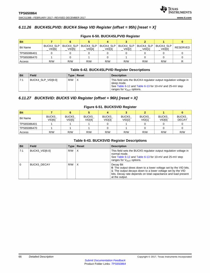
66
TPS650864SWCS138B –FEBRUARY 2017–REVISED DECEMBER 2017 www.ti.com
Submit Documentation FeedbackProduct Folder Links: TPS650864
Detailed Description Copyright © 2017, Texas Instruments Incorporated
6.11.26 BUCK4SLPVID: BUCK4 Sleep VID Register (offset = 95h) [reset = X]
Figure 6-50. BUCK4SLPVID RegisterBit 7 6 5 4 3 2 1 0
Bit Name BUCK4_SLP_ VID[6]
BUCK4_SLP_ VID[5]
BUCK4_SLP_ VID[4]
BUCK4_SLP_ VID[3]
BUCK4_SLP_ VID[2]
BUCK4_SLP_ VID[1]
BUCK4_SLP_ VID[0] RESERVED
TPS65086401 0 0 0 0 0 0 0 0TPS65086470 1 0 1 0 1 0 0 0Access R/W R/W R/W R/W R/W R/W R/W R
Table 6-42. BUCK4SLPVID Register DescriptionsBit Field Type Reset Description7:1 BUCK4_SLP_VID[6:0] R/W X This field sets the BUCK4 regulator output regulation voltage in
sleep mode.See Table 6-12 and Table 6-13 for 10-mV and 25-mV stepranges for VOUT options.
6.11.27 BUCK5VID: BUCK5 VID Register (offset = 96h) [reset = X]
Figure 6-51. BUCK5VID RegisterBit 7 6 5 4 3 2 1 0
Bit Name BUCK5_VID[6]
BUCK5_VID[5]
BUCK5_VID[4]
BUCK5_VID[3]
BUCK5_VID[2]
BUCK5_VID[1]
BUCK5_VID[0]
BUCK5_DECAY
TPS65086401 1 1 1 0 1 0 0 0TPS65086470 1 1 1 0 1 0 0 0Access R/W R/W R/W R/W R/W R/W R/W R/W
Table 6-43. BUCK5VID Register DescriptionsBit Field Type Reset Description7:1 BUCK5_VID[6:0] R/W X This field sets the BUCK5 regulator output regulation voltage in
normal mode.See Table 6-12 and Table 6-13 for 10-mV and 25-mV stepranges for VOUT options.
0 BUCK5_DECAY R/W X Decay Bit0: The output slews down to a lower voltage set by the VID bits.1: The output decays down to a lower voltage set by the VIDbits. Decay rate depends on total capacitance and load presentat the output.

67
TPS650864www.ti.com SWCS138B –FEBRUARY 2017–REVISED DECEMBER 2017
Submit Documentation FeedbackProduct Folder Links: TPS650864
Detailed DescriptionCopyright © 2017, Texas Instruments Incorporated
6.11.28 BUCK5SLPVID: BUCK5 Sleep VID Register (offset = 97h) [reset = X]
Figure 6-52. BUCK5SLPVID RegisterBit 7 6 5 4 3 2 1 0
Bit Name BUCK5_SLP_ VID[6]
BUCK5_SLP_ VID[5]
BUCK5_SLP_ VID[4]
BUCK5_SLP_ VID[3]
BUCK5_SLP_ VID[2]
BUCK5_SLP_ VID[1]
BUCK5_SLP_ VID[0] RESERVED
TPS65086401 1 1 1 0 1 0 0 0TPS65086470 1 1 1 0 1 0 0 0Access R/W R/W R/W R/W R/W R/W R/W R
Table 6-44. BUCK5SLPVID Register DescriptionsBit Field Type Reset Description7:1 BUCK5_SLP_VID[6:0] R/W X This field sets the BUCK5 regulator output regulation voltage in
sleep mode.See Table 6-12 and Table 6-13 for 10-mV and 25-mV stepranges for VOUT options.
6.11.29 BUCK6VID: BUCK6 VID Register (offset = 98h) [reset = X]
Figure 6-53. BUCK6VID RegisterBit 7 6 5 4 3 2 1 0
Bit Name BUCK6_VID[6]
BUCK6_VID[5]
BUCK6_VID[4]
BUCK6_VID[3]
BUCK6_VID[2]
BUCK6_VID[1]
BUCK6_VID[0]
BUCK6_DECAY
TPS65086401 1 1 0 1 1 1 0 0TPS65086470 0 1 0 1 1 0 0 0Access R/W R/W R/W R/W R/W R/W R/W R/W
Table 6-45. BUCK6VID Register DescriptionsBit Field Type Reset Description7:1 BUCK6_VID[6:0] R/W X This field sets the BUCK6 regulator output regulation voltage in
normal mode.See Table 6-12 and Table 6-13 for 10-mV and 25-mV step rangesfor VOUT options.
0 BUCK6_DECAY R/W X Decay Bit0: The output slews down to a lower voltage set by the VID bits.1: The output decays down to a lower voltage set by the VID bits.Decay rate depends on total capacitance and load present at theoutput.

68
TPS650864SWCS138B –FEBRUARY 2017–REVISED DECEMBER 2017 www.ti.com
Submit Documentation FeedbackProduct Folder Links: TPS650864
Detailed Description Copyright © 2017, Texas Instruments Incorporated
6.11.30 BUCK6SLPVID: BUCK6 Sleep VID Register (offset = 99h) [reset = X]
Figure 6-54. BUCK6SLPVID RegisterBit 7 6 5 4 3 2 1 0
Bit Name BUCK6_SLP_ VID[6]
BUCK6_SLP_ VID[5]
BUCK6_SLP_ VID[4]
BUCK6_SLP_ VID[3]
BUCK6_SLP_ VID[2]
BUCK6_SLP_ VID[1]
BUCK6_SLP_ VID[0] RESERVED
TPS65086401 1 0 0 0 1 1 0 0TPS65086470 0 1 0 0 1 1 0 0Access R/W R/W R/W R/W R/W R/W R/W R
Table 6-46. BUCK6SLPVID Register DescriptionsBit Field Type Reset Description7:1 BUCK6_SLP_VID[6:0] R/W X This field sets the BUCK6 regulator output regulation voltage in
normal mode.See Table 6-12 and Table 6-13 for 10-mV and 25-mV stepranges for VOUT options.
6.11.31 LDOA2VID: LDOA2 VID Register (offset = 9Ah) [reset = X]
Figure 6-55. LDOA2VID RegisterBit 7 6 5 4 3 2 1 0
Bit Name LDOA2_SLP_VID[3]
LDOA2_SLP_VID[2]
LDOA2_SLP_VID[1]
LDOA2_SLP_VID[0]
LDOA2_VID[3]
LDOA2_VID[3]
LDOA2_VID[1]
LDOA2_VID[0]
TPS65086401 1 0 1 0 1 0 1 0TPS65086470 0 0 0 0 0 0 0 0Access R/W R/W R/W R/W R/W R/W R/W R/W
Table 6-47. LDOA2VID Register DescriptionsBit Field Type Reset Description7:4 LDOA2_SLP_VID[3:0] R/W X This field sets the LDOA2 regulator output regulation voltage in
sleep mode.See Table 6-15 for Vout options.
3:0 LDOA2_VID[3:0] R/W X This field sets the LDOA2 regulator output regulation voltage innormal mode.See Table 6-15 for Vout options.
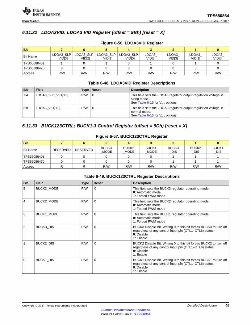
69
TPS650864www.ti.com SWCS138B –FEBRUARY 2017–REVISED DECEMBER 2017
Submit Documentation FeedbackProduct Folder Links: TPS650864
Detailed DescriptionCopyright © 2017, Texas Instruments Incorporated
6.11.32 LDOA3VID: LDOA3 VID Register (offset = 9Bh) [reset = X]
Figure 6-56. LDOA3VID RegisterBit 7 6 5 4 3 2 1 0
Bit Name LDOA3_SLP_ VID[3]
LDOA3_SLP_ VID[2]
LDOA3_SLP_ VID[1]
LDOA3_SLP_ VID[0]
LDOA3_VID[3]
LDOA3_VID[3]
LDOA3_VID[1]
LDOA3_VID[0]
TPS65086401 1 0 1 0 1 0 1 0TPS65086470 0 0 0 0 0 0 0 0Access R/W R/W R/W R/W R/W R/W R/W R/W
Table 6-48. LDOA3VID Register DescriptionsBit Field Type Reset Description7:4 LDOA3_SLP_VID[3:0] R/W X This field sets the LDOA3 regulator output regulation voltage in
sleep mode.See Table 6-15 for Vout options.
3:0 LDOA3_VID[3:0] R/W X This field sets the LDOA3 regulator output regulation voltage innormal mode.See Table 6-15 for Vout options.
6.11.33 BUCK123CTRL: BUCK1-3 Control Register (offset = 9Ch) [reset = X]
Figure 6-57. BUCK123CTRL RegisterBit 7 6 5 4 3 2 1 0
Bit Name RESERVED RESERVED BUCK3_MODE
BUCK2_MODE
BUCK1_MODE
BUCK3_DIS
BUCK2_DIS
BUCK1_DIS
TPS65086401 0 0 0 0 0 1 1 1TPS65086470 0 0 0 0 0 1 1 1Access R R R/W R/W R/W R/W R/W R/W
Table 6-49. BUCK123CTRL Register DescriptionsBit Field Type Reset Description5 BUCK3_MODE R/W X This field sets the BUCK3 regulator operating mode.
0: Automatic mode1: Forced PWM mode
4 BUCK2_MODE R/W X This field sets the BUCK2 regulator operating mode.0: Automatic mode1: Forced PWM mode
3 BUCK1_MODE R/W X This field sets the BUCK1 regulator operating mode.0: Automatic mode1: Forced PWM mode
2 BUCK3_DIS R/W X BUCK3 Disable Bit. Writing 0 to this bit forces BUCK3 to turn offregardless of any control input pin (CTL1–CTL6) status.0: Disable1: Enable
1 BUCK2_DIS R/W X BUCK2 Disable Bit. Writing 0 to this bit forces BUCK2 to turn offregardless of any control input pin (CTL1–CTL6) status.0: Disable1: Enable
0 BUCK1_DIS R/W X BUCK1 Disable Bit. Writing 0 to this bit forces BUCK1 to turn offregardless of any control input pin (CTL1–CTL6) status.0: Disable1: Enable

70
TPS650864SWCS138B –FEBRUARY 2017–REVISED DECEMBER 2017 www.ti.com
Submit Documentation FeedbackProduct Folder Links: TPS650864
Detailed Description Copyright © 2017, Texas Instruments Incorporated
6.11.34 PG_DELAY2: 2nd Power Good Delay Register (offset = 9Dh) [reset = X]Programmable Power Good delay for GPO1, GPO2, and GPO4 pins, measured from the moment whenall VRs assigned to respective GPO reach their regulation range to Power Good assertion. This is anoptional register as the PMIC can be programmed for system PG, level shifter or I2C controller GPO.
Figure 6-58. PG_DELAY2 RegisterBit 7 6 5 4 3 2 1 0
Bit Name GPO2_PG_DELAY[2]
GPO2_PG_DELAY[1]
GPO2_PG_DELAY[0]
GPO4_PG_DELAY[2]
GPO4_PG_DELAY[1]
GPO4_PG_DELAY[0]
GPO1_PG_DELAY[1]
GPO1_PG_DELAY[0]
TPS65086401 0 0 0 0 0 0 0 0TPS65086470 0 0 0 X X X 0 0Access R/W R/W R/W R/W R/W R/W R/W R/W
Table 6-50. PG_DELAY2 Register DescriptionsBit Field Type Reset Description7:5 GPO2_PG_DELAY[2:0] R/W X Programmable delay Power Good or level shifter for GPO2 pin.
Measured from the moment when all rails grouped to this pinreach their regulation range. All values have ±10% variation.000: 0 ms
001: 5.0 ms010: 10 ms011: 15 ms100: 20 ms101: 50 ms110: 75 ms111: 100 msXXX: Bits not used. If GPO2 is controlled by I2C rather than PGand is not used internally for VTT LDO enable, these bits have noimpact. Default is set to '0'.
4:2 GPO4_PG_DELAY[2:0] R/W X Programmable delay Power Good or level shifter for GPO4 pin.Measured from the moment when all rails grouped to this pinreach their regulation range. All values have ±10% variation.000: 0 ms
001: 5.0 ms010: 10 ms011: 15 ms100: 20 ms101: 50 ms110: 75 ms111: 100 msXXX: Bits not used. If GPO4 is controlled by I2C rather than PG,these bits have no impact. Default is set to '0'.
1:0 GPO1_PG_DELAY[1:0] R/W X Programmable delay Power Good or level shifter for GPO1 pin.Measured from the moment when all rails grouped to this pinreach their regulation range. All values have ±10% variation.00: 0 ms01: 5.0 ms10: 10 ms11: 15 msXX: Bits not used. If GPO1 is controlled by I2C rather than PG,these bits have no impact. Default is set to '0'.
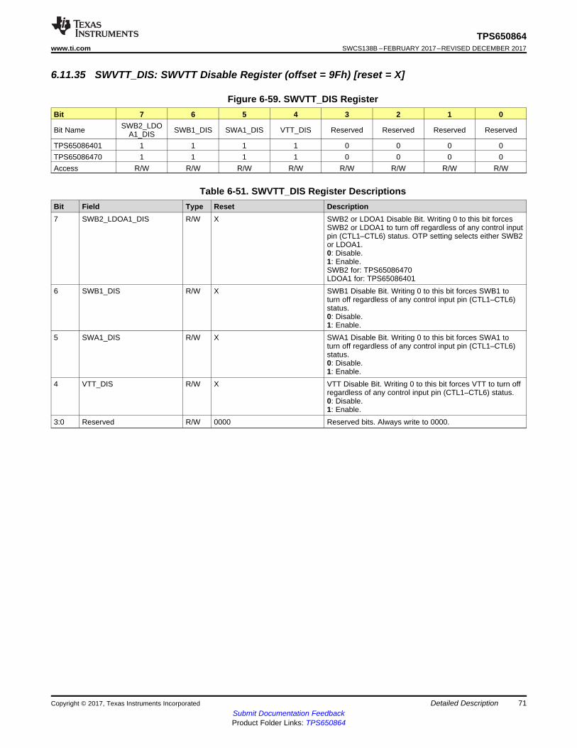
71
TPS650864www.ti.com SWCS138B –FEBRUARY 2017–REVISED DECEMBER 2017
Submit Documentation FeedbackProduct Folder Links: TPS650864
Detailed DescriptionCopyright © 2017, Texas Instruments Incorporated
6.11.35 SWVTT_DIS: SWVTT Disable Register (offset = 9Fh) [reset = X]
Figure 6-59. SWVTT_DIS RegisterBit 7 6 5 4 3 2 1 0
Bit Name SWB2_LDOA1_DIS SWB1_DIS SWA1_DIS VTT_DIS Reserved Reserved Reserved Reserved
TPS65086401 1 1 1 1 0 0 0 0TPS65086470 1 1 1 1 0 0 0 0Access R/W R/W R/W R/W R/W R/W R/W R/W
Table 6-51. SWVTT_DIS Register DescriptionsBit Field Type Reset Description7 SWB2_LDOA1_DIS R/W X SWB2 or LDOA1 Disable Bit. Writing 0 to this bit forces
SWB2 or LDOA1 to turn off regardless of any control inputpin (CTL1–CTL6) status. OTP setting selects either SWB2or LDOA1.0: Disable.1: Enable.SWB2 for: TPS65086470LDOA1 for: TPS65086401
6 SWB1_DIS R/W X SWB1 Disable Bit. Writing 0 to this bit forces SWB1 toturn off regardless of any control input pin (CTL1–CTL6)status.0: Disable.1: Enable.
5 SWA1_DIS R/W X SWA1 Disable Bit. Writing 0 to this bit forces SWA1 toturn off regardless of any control input pin (CTL1–CTL6)status.0: Disable.1: Enable.
4 VTT_DIS R/W X VTT Disable Bit. Writing 0 to this bit forces VTT to turn offregardless of any control input pin (CTL1–CTL6) status.0: Disable.1: Enable.
3:0 Reserved R/W 0000 Reserved bits. Always write to 0000.
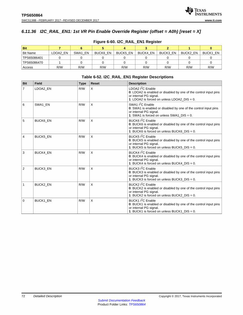
72
TPS650864SWCS138B –FEBRUARY 2017–REVISED DECEMBER 2017 www.ti.com
Submit Documentation FeedbackProduct Folder Links: TPS650864
Detailed Description Copyright © 2017, Texas Instruments Incorporated
6.11.36 I2C_RAIL_EN1: 1st VR Pin Enable Override Register (offset = A0h) [reset = X]
Figure 6-60. I2C_RAIL_EN1 RegisterBit 7 6 5 4 3 2 1 0Bit Name LDOA2_EN SWA1_EN BUCK6_EN BUCK5_EN BUCK4_EN BUCK3_EN BUCK2_EN BUCK1_ENTPS65086401 0 0 0 0 0 0 0 0TPS65086470 1 0 0 0 0 0 0 0Access R/W R/W R/W R/W R/W R/W R/W R/W
Table 6-52. I2C_RAIL_EN1 Register DescriptionsBit Field Type Reset Description7 LDOA2_EN R/W X LDOA2 I2C Enable
0: LDOA2 is enabled or disabled by one of the control input pinsor internal PG signal.1: LDOA2 is forced on unless LDOA2_DIS = 0.
6 SWA1_EN R/W X SWA1 I2C Enable0: SWA1 is enabled or disabled by one of the control input pinsor internal PG signal.1: SWA1 is forced on unless SWA1_DIS = 0.
5 BUCK6_EN R/W X BUCK6 I2C Enable0: BUCK6 is enabled or disabled by one of the control input pinsor internal PG signal.1: BUCK6 is forced on unless BUCK6_DIS = 0.
4 BUCK5_EN R/W X BUCK5 I2C Enable0: BUCK5 is enabled or disabled by one of the control input pinsor internal PG signal.1: BUCK5 is forced on unless BUCK5_DIS = 0.
3 BUCK4_EN R/W X BUCK4 I2C Enable0: BUCK4 is enabled or disabled by one of the control input pinsor internal PG signal.1: BUCK4 is forced on unless BUCK4_DIS = 0.
2 BUCK3_EN R/W X BUCK3 I2C Enable0: BUCK3 is enabled or disabled by one of the control input pinsor internal PG signal.1: BUCK3 is forced on unless BUCK3_DIS = 0.
1 BUCK2_EN R/W X BUCK2 I2C Enable0: BUCK2 is enabled or disabled by one of the control input pinsor internal PG signal.1: BUCK2 is forced on unless BUCK2_DIS = 0.
0 BUCK1_EN R/W X BUCK1 I2C Enable0: BUCK1 is enabled or disabled by one of the control input pinsor internal PG signal.1: BUCK1 is forced on unless BUCK1_DIS = 0.
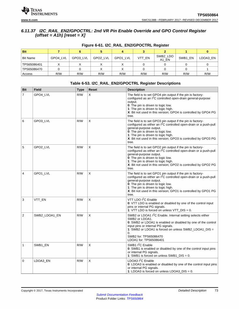
73
TPS650864www.ti.com SWCS138B –FEBRUARY 2017–REVISED DECEMBER 2017
Submit Documentation FeedbackProduct Folder Links: TPS650864
Detailed DescriptionCopyright © 2017, Texas Instruments Incorporated
6.11.37 I2C_RAIL_EN2/GPOCTRL: 2nd VR Pin Enable Override and GPO Control Register(offset = A1h) [reset = X]
Figure 6-61. I2C_RAIL_EN2/GPOCTRL RegisterBit 7 6 5 4 3 2 1 0
Bit Name GPO4_LVL GPO3_LVL GPO2_LVL GPO1_LVL VTT_EN SWB2_LDOA1_EN SWB1_EN LDOA3_EN
TPS65086401 X X X X 0 0 0 0TPS65086470 0 0 X X 0 0 0 1Access R/W R/W R/W R/W R/W R/W R/W R/W
Table 6-53. I2C_RAIL_EN2/GPOCTRL Register DescriptionsBit Field Type Reset Description7 GPO4_LVL R/W X The field is to set GPO4 pin output if the pin is factory-
configured as an I2C controlled open-drain general-purposeoutput.0: The pin is driven to logic low.1: The pin is driven to logic high.X: Bit not used in this version; GPO4 is controlled by GPO4 PGtree.
6 GPO3_LVL R/W X The field is to set GPO3 pin output if the pin is factory-configured as either an I2C controlled open-drain or a push-pullgeneral-purpose output.0: The pin is driven to logic low.1: The pin is driven to logic high.X: Bit not used in this version; GPO3 is controlled by GPO3 PGtree.
5 GPO2_LVL R/W X The field is to set GPO2 pin output if the pin is factory-configured as either an I2C controlled open-drain or a push-pullgeneral-purpose output.0: The pin is driven to logic low.1: The pin is driven to logic high.X: Bit not used in this version; GPO2 is controlled by GPO2 PGtree.
4 GPO1_LVL R/W X The field is to set GPO1 pin output if the pin is factory-configured as either an I2C controlled open-drain or a push-pullgeneral-purpose output.0: The pin is driven to logic low.1: The pin is driven to logic high.X: Bit not used in this version; GPO1 is controlled by GPO1 PGtree.
3 VTT_EN R/W X VTT LDO I2C Enable0: VTT LDO is enabled or disabled by one of the control inputpins or internal PG signals.1: VTT LDO is forced on unless VTT_DIS = 0.
2 SWB2_LDOA1_EN R/W X SWB2 or LDOA1 I2C Enable. Internal setting selects eitherSWB2 or LDOA1.0: SWB2 or LDOA1 is enabled or disabled by one of the controlinput pins or internal PG signals.1: SWB2 or LDOA1 is forced on unless SWB2_LDOA1_DIS =0.SWB2 for: TPS65086470LDOA1 for: TPS65086401
1 SWB1_EN R/W X SWB1 I2C Enable0: SWB1 is enabled or disabled by one of the control input pinsor internal PG signals.1: SWB1 is forced on unless SWB1_DIS = 0.
0 LDOA3_EN R/W X LDOA3 I2C Enable0: LDOA3 is enabled or disabled by one of the control input pinsor internal PG signals.1: LDOA3 is forced on unless LDOA3_DIS = 0.

74
TPS650864SWCS138B –FEBRUARY 2017–REVISED DECEMBER 2017 www.ti.com
Submit Documentation FeedbackProduct Folder Links: TPS650864
Detailed Description Copyright © 2017, Texas Instruments Incorporated
6.11.38 PWR_FAULT_MASK1: 1st VR Power Fault Mask Register (offset = A2h) [reset = X]
Figure 6-62. PWR_FAULT_MASK1 RegisterBit 7 6 5 4 3 2 1 0
Bit Name LDOA2_FLTMSK
SWA1_FLTMSK
BUCK6_FLTMSK
BUCK5_FLTMSK
BUCK4_FLTMSK
BUCK3_FLTMSK
BUCK2_FLTMSK
BUCK1_FLTMSK
TPS65086401 0 0 0 0 0 0 0 0TPS65086470 1 1 0 0 0 0 0 0Access R/W R/W R/W R/W R/W R/W R/W R/W
Table 6-54. PWR_FAULT_MASK1 Register DescriptionsBit Field Type Reset Description7 LDOA2_FLTMSK R/W X LDOA2 Power Fault Mask. When masked, power fault from
LDOA2 does not cause PMIC to shutdown.0: Not Masked1: Masked
6 SWA1_FLTMSK R/W X SWA1 Power Fault Mask. When masked, power fault from SWA1does not cause PMIC to shutdown.0: Not Masked1: Masked
5 BUCK6_FLTMSK R/W X BUCK6 Power Fault Mask. When masked, power fault fromBUCK6 does not cause PMIC to shutdown.0: Not Masked1: Masked
4 BUCK5_FLTMSK R/W X BUCK5 Power Fault Mask. When masked, power fault fromBUCK5 does not cause PMIC to shutdown.0: Not Masked1: Masked
3 BUCK4_FLTMSK R/W X BUCK4 Power Fault Mask. When masked, power fault fromBUCK4 does not cause PMIC to shutdown.0: Not Masked1: Masked
2 BUCK3_FLTMSK R/W X BUCK3 Power Fault Mask. When masked, power fault fromBUCK3 does not cause PMIC to shutdown.0: Not Masked1: Masked
1 BUCK2_FLTMSK R/W X BUCK2 Power Fault Mask. When masked, power fault fromBUCK2 does not cause PMIC to shutdown.0: Not Masked1: Masked
0 BUCK1_FLTMSK R/W X BUCK1 Power Fault Mask. When masked, power fault fromBUCK1 does not cause PMIC to shutdown.0: Not Masked1: Masked

75
TPS650864www.ti.com SWCS138B –FEBRUARY 2017–REVISED DECEMBER 2017
Submit Documentation FeedbackProduct Folder Links: TPS650864
Detailed DescriptionCopyright © 2017, Texas Instruments Incorporated
6.11.39 PWR_FAULT_MASK2: 2nd VR Power Fault Mask Register (offset = A3h) [reset = X]
Figure 6-63. PWR_FAULT_MASK2 RegisterBit 7 6 5 4 3 2 1 0
Bit Name RESERVED RESERVED RESERVED LDOA1_FLTMSK
VTT_FLTMSK
SWB2_FLTMSK
SWB1_FLTMSK
LDOA3_FLTMSK
TPS65086401 0 0 1 0 1 0 0 0TPS65086470 0 0 1 1 0 1 1 1Access R R/W R/W R/W R/W R/W R/W R/W
Table 6-55. PWR_FAULT_MASK2 Register DescriptionsBit Field Type Reset Description6 RESERVED R/W 0 Reserved bit. Always write to '0'.5 RESERVED R/W 1 Reserved bit. Always write to '1'.4 LDOA1_FLTMSK R/W X LDOA1 Power Fault Mask. When masked, power fault from
LDOA1 does not cause PMIC to shutdown.0: Not Masked1: Masked
3 VTT_FLTMSK R/W X VTT LDO Power Fault Mask. When masked, power fault fromVTT LDO does not cause PMIC to shutdown.0: Not Masked1: Masked
2 SWB2_FLTMSK R/W X SWB2 Power Fault Mask. When masked, power fault fromSWB2 does not cause PMIC to shutdown.0: Not Masked1: Masked
1 SWB1_FLTMSK R/W X SWB1 Power Fault Mask. When masked, power fault fromSWB1 does not cause PMIC to shutdown.0: Not Masked1: Masked
0 LDOA3_FLTMSK R/W X LDOA3 Power Fault Mask. When masked, power fault fromLDOA3 does not cause PMIC to shutdown.0: Not Masked1: Masked

76
TPS650864SWCS138B –FEBRUARY 2017–REVISED DECEMBER 2017 www.ti.com
Submit Documentation FeedbackProduct Folder Links: TPS650864
Detailed Description Copyright © 2017, Texas Instruments Incorporated
6.11.40 GPO1PG_CTRL1: 1st GPO1 PG Control Register (offset = A4h) [reset = X]
Figure 6-64. GPO1PG_CTRL1 RegisterBit 7 6 5 4 3 2 1 0
Bit Name LDOA2_MSK
SWA1_MSK
BUCK6_MSK
BUCK5_MSK
BUCK4_MSK
BUCK3_MSK
BUCK2_MSK
BUCK1_MSK
TPS65086401 0 1 0 1 1 1 0 0TPS65086470 1 1 1 1 1 1 0 0Access R/W R/W R/W R/W R/W R/W R/W R/W
Table 6-56. GPO1PG_CTRL1 Register DescriptionsBit Field Type Reset Description7 LDOA2_MSK R/W X 0: LDOA2 PG is part of Power Good tree of GPO1 pin.
1: LDOA2 PG is NOT part of Power Good tree of GPO1 pin andis ignored.
6 SWA1_MSK R/W X 0: SWA1 PG is part of Power Good tree of GPO1 pin.1: SWA1 PG is NOT part of Power Good tree of GPO1 pin andis ignored.
5 BUCK6_MSK R/W X 0: BUCK6 PG is part of Power Good tree of GPO1 pin.1: BUCK6 PG is NOT part of Power Good tree of GPO1 pin andis ignored.
4 BUCK5_MSK R/W X 0: BUCK5 PG is part of Power Good tree of GPO1 pin.1: BUCK5 PG is NOT part of Power Good tree of GPO1 pin andis ignored.
3 BUCK4_MSK R/W X 0: BUCK4 PG is part of Power Good tree of GPO1 pin.1: BUCK4 PG is NOT part of Power Good tree of GPO1 pin andis ignored.
2 BUCK3_MSK R/W X 0: BUCK3 PG is part of Power Good tree of GPO1 pin.1: BUCK3 PG is NOT part of Power Good tree of GPO1 pin andis ignored.
1 BUCK2_MSK R/W X 0: BUCK2 PG is part of Power Good tree of GPO1 pin.1: BUCK2 PG is NOT part of Power Good tree of GPO1 pin andis ignored.
0 BUCK1_MSK R/W X 0: BUCK1 PG is part of Power Good tree of GPO1 pin.1: BUCK1 PG is NOT part of Power Good tree of GPO1 pin andis ignored.

77
TPS650864www.ti.com SWCS138B –FEBRUARY 2017–REVISED DECEMBER 2017
Submit Documentation FeedbackProduct Folder Links: TPS650864
Detailed DescriptionCopyright © 2017, Texas Instruments Incorporated
6.11.41 GPO1PG_CTRL2: 2nd GPO1 PG Control Register (offset = A5h) [reset = X]
Figure 6-65. GPO1PG_CTRL2 RegisterBit 7 6 5 4 3 2 1 0
Bit Name CTL5_MSK CTL4_MSK CTL2_MSK CTL1_MSK VTT_MSK SWB2_LDOA1_MSK SWB1_MSK LDOA3_MSK
TPS65086401 1 1 1 0 1 0 1 1TPS65086470 1 1 1 0 1 1 1 1Access R/W R/W R/W R/W R/W R/W R/W R/W
Table 6-57. GPO1PG_CTRL2 Register DescriptionsBit Field Type Reset Description7 CTL5_MSK R/W X 0: CTL5 pin status is part of Power Good tree of GPO1 pin.
1: CTL5 pin status is NOT part of Power Good tree of GPO1 pinand is ignored.
6 CTL4_MSK R/W X 0: CTL4 pin status is part of Power Good tree of GPO1 pin.1: CTL4 pin status is NOT part of Power Good tree of GPO1 pinand is ignored.
5 CTL2_MSK R/W X 0: CTL2 pin status is part of Power Good tree of GPO1 pin.1: CTL2 pin status is NOT part of Power Good tree of GPO1 pinand is ignored.
4 CTL1_MSK R/W X 0: CTL1 pin status is part of Power Good tree of GPO1 pin.1: CTL1 pin status is NOT part of Power Good tree of GPO1 pinand is ignored.
3 VTT_MSK R/W X 0: VTT LDO PG is part of Power Good tree of GPO1 pin.1: VTT LDO PG is NOT part of Power Good tree of GPO1 pinand is ignored.
2 SWB2_LDOA1_MSK R/W X 0: SWB2_LDOA1 PG is part of Power Good tree of GPO1 pin.1: SWB2_LDOA1 PG is NOT part of Power Good tree of GPO1pin and is ignored.SWB2 for: TPS65086470LDOA1 for:TPS65086401
1 SWB1_MSK R/W X 0: SWB1 PG is part of Power Good tree of GPO1 pin.1: SWB1 PG is NOT part of Power Good tree of GPO1 pin andis ignored.
0 LDOA3_MSK R/W X 0: LDOA3 PG is part of Power Good tree of GPO1 pin.1: LDOA3 PG is NOT part of Power Good tree of GPO1 pin andis ignored.
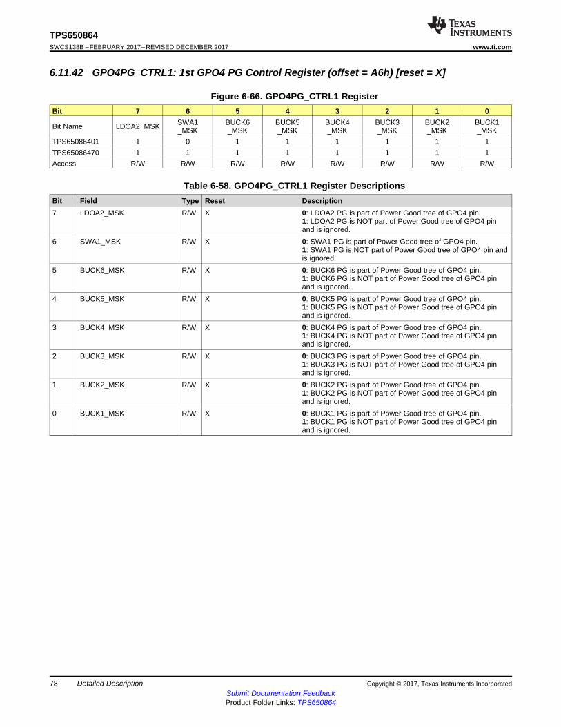
78
TPS650864SWCS138B –FEBRUARY 2017–REVISED DECEMBER 2017 www.ti.com
Submit Documentation FeedbackProduct Folder Links: TPS650864
Detailed Description Copyright © 2017, Texas Instruments Incorporated
6.11.42 GPO4PG_CTRL1: 1st GPO4 PG Control Register (offset = A6h) [reset = X]
Figure 6-66. GPO4PG_CTRL1 RegisterBit 7 6 5 4 3 2 1 0
Bit Name LDOA2_MSK SWA1_MSK
BUCK6_MSK
BUCK5_MSK
BUCK4_MSK
BUCK3_MSK
BUCK2_MSK
BUCK1_MSK
TPS65086401 1 0 1 1 1 1 1 1TPS65086470 1 1 1 1 1 1 1 1Access R/W R/W R/W R/W R/W R/W R/W R/W
Table 6-58. GPO4PG_CTRL1 Register DescriptionsBit Field Type Reset Description7 LDOA2_MSK R/W X 0: LDOA2 PG is part of Power Good tree of GPO4 pin.
1: LDOA2 PG is NOT part of Power Good tree of GPO4 pinand is ignored.
6 SWA1_MSK R/W X 0: SWA1 PG is part of Power Good tree of GPO4 pin.1: SWA1 PG is NOT part of Power Good tree of GPO4 pin andis ignored.
5 BUCK6_MSK R/W X 0: BUCK6 PG is part of Power Good tree of GPO4 pin.1: BUCK6 PG is NOT part of Power Good tree of GPO4 pinand is ignored.
4 BUCK5_MSK R/W X 0: BUCK5 PG is part of Power Good tree of GPO4 pin.1: BUCK5 PG is NOT part of Power Good tree of GPO4 pinand is ignored.
3 BUCK4_MSK R/W X 0: BUCK4 PG is part of Power Good tree of GPO4 pin.1: BUCK4 PG is NOT part of Power Good tree of GPO4 pinand is ignored.
2 BUCK3_MSK R/W X 0: BUCK3 PG is part of Power Good tree of GPO4 pin.1: BUCK3 PG is NOT part of Power Good tree of GPO4 pinand is ignored.
1 BUCK2_MSK R/W X 0: BUCK2 PG is part of Power Good tree of GPO4 pin.1: BUCK2 PG is NOT part of Power Good tree of GPO4 pinand is ignored.
0 BUCK1_MSK R/W X 0: BUCK1 PG is part of Power Good tree of GPO4 pin.1: BUCK1 PG is NOT part of Power Good tree of GPO4 pinand is ignored.

79
TPS650864www.ti.com SWCS138B –FEBRUARY 2017–REVISED DECEMBER 2017
Submit Documentation FeedbackProduct Folder Links: TPS650864
Detailed DescriptionCopyright © 2017, Texas Instruments Incorporated
6.11.43 GPO4PG_CTRL2: 2nd GPO4 PG Control Register (offset = A7h) [reset = X]
Figure 6-67. GPO4PG_CTRL2 RegisterBit 7 6 5 4 3 2 1 0
Bit Name CTL5_MSK CTL4_MSK CTL2_MSK CTL1_MSK VTT_MSK SWB2_LDOA1_MSK SWB1_MSK LDOA3_MSK
TPS65086401 1 1 1 1 1 1 1 1TPS65086470 1 1 1 1 1 1 1 1Access R/W R/W R/W R/W R/W R/W R/W R/W
Table 6-59. GPO4PG_CTRL2 Register DescriptionsrBit Field Type Reset Description7 CTL5_MSK R/W X 0: CTL5 pin status is part of Power Good tree of GPO4 pin.
1: CTL5 pin status is NOT part of Power Good tree of GPO4 pinand is ignored.
6 CTL4_MSK R/W X 0: CTL4 pin status is part of Power Good tree of GPO4 pin.1: CTL4 pin status is NOT part of Power Good tree of GPO4 pinand is ignored.
5 CTL2_MSK R/W X 0: CTL2 pin status is part of Power Good tree of GPO4 pin.1: CTL2 pin status is NOT part of Power Good tree of GPO4 pinand is ignored.
4 CTL1_MSK R/W X 0: CTL1 pin status is part of Power Good tree of GPO4 pin.1: CTL1 pin status is NOT part of Power Good tree of GPO4 pinand is ignored.
3 VTT_MSK R/W X 0: VTT LDO PG is part of Power Good tree of GPO4 pin.1: VTT LDO PG is NOT part of Power Good tree of GPO4 pinand is ignored.
2 SWB2_LDOA1_MSK R/W X 0: SWB2_LDOA1 PG is part of Power Good tree of GPO4 pin.1: SWB2_LDOA1 PG is NOT part of Power Good tree of GPO4pin and is ignored.SWB2 for: TPS65086470LDOA1 for: TPS65086401
1 SWB1_MSK R/W X 0: SWB1 PG is part of Power Good tree of GPO4 pin.1: SWB1 PG is NOT part of Power Good tree of GPO4 pin andis ignored.
0 LDOA3_MSK R/W X 0: LDOA3 PG is part of Power Good tree of GPO4 pin.1: LDOA3 PG is NOT part of Power Good tree of GPO4 pin andis ignored.

80
TPS650864SWCS138B –FEBRUARY 2017–REVISED DECEMBER 2017 www.ti.com
Submit Documentation FeedbackProduct Folder Links: TPS650864
Detailed Description Copyright © 2017, Texas Instruments Incorporated
6.11.44 GPO2PG_CTRL1: 1st GPO2 PG Control Register (offset = A8h) [reset = X]
Figure 6-68. GPO2PG_CTRL1 RegisterBit 7 6 5 4 3 2 1 0
Bit Name LDOA2_MSK SWA1_MSK
BUCK6_MSK
BUCK5_MSK
BUCK4_MSK
BUCK3_MSK
BUCK2_MSK
BUCK1_MSK
TPS65086401 1 1 1 0 1 0 1 1TPS65086470 1 1 0 0 0 0 0 0Access R/W R/W R/W R/W R/W R/W R/W R/W
Table 6-60. GPO2PG_CTRL1 Register DescriptionsBit Field Type Reset Description7 LDOA2_MSK R/W X 0: LDOA2 PG is part of Power Good tree of GPO2 pin.
1: LDOA2 PG is NOT part of Power Good tree of GPO2 pinand is ignored.
6 SWA1_MSK R/W X 0: SWA1 PG is part of Power Good tree of GPO2 pin.1: SWA1 PG is NOT part of Power Good tree of GPO2 pinand is ignored.
5 BUCK6_MSK R/W X 0: BUCK6 PG is part of Power Good tree of GPO2 pin.1: BUCK6 PG is NOT part of Power Good tree of GPO2 pinand is ignored.
4 BUCK5_MSK R/W X 0: BUCK5 PG is part of Power Good tree of GPO2 pin.1: BUCK5 PG is NOT part of Power Good tree of GPO2 pinand is ignored.
3 BUCK4_MSK R/W X 0: BUCK4 PG is part of Power Good tree of GPO2 pin.1: BUCK4 PG is NOT part of Power Good tree of GPO2 pinand is ignored.
2 BUCK3_MSK R/W X 0: BUCK3 PG is part of Power Good tree of GPO2 pin.1: BUCK3 PG is NOT part of Power Good tree of GPO2 pinand is ignored.
1 BUCK2_MSK R/W X 0: BUCK2 PG is part of Power Good tree of GPO2 pin.1: BUCK2 PG is NOT part of Power Good tree of GPO2 pinand is ignored.
0 BUCK1_MSK R/W X 0: BUCK1 PG is part of Power Good tree of GPO2 pin.1: BUCK1 PG is NOT part of Power Good tree of GPO2 pinand is ignored.
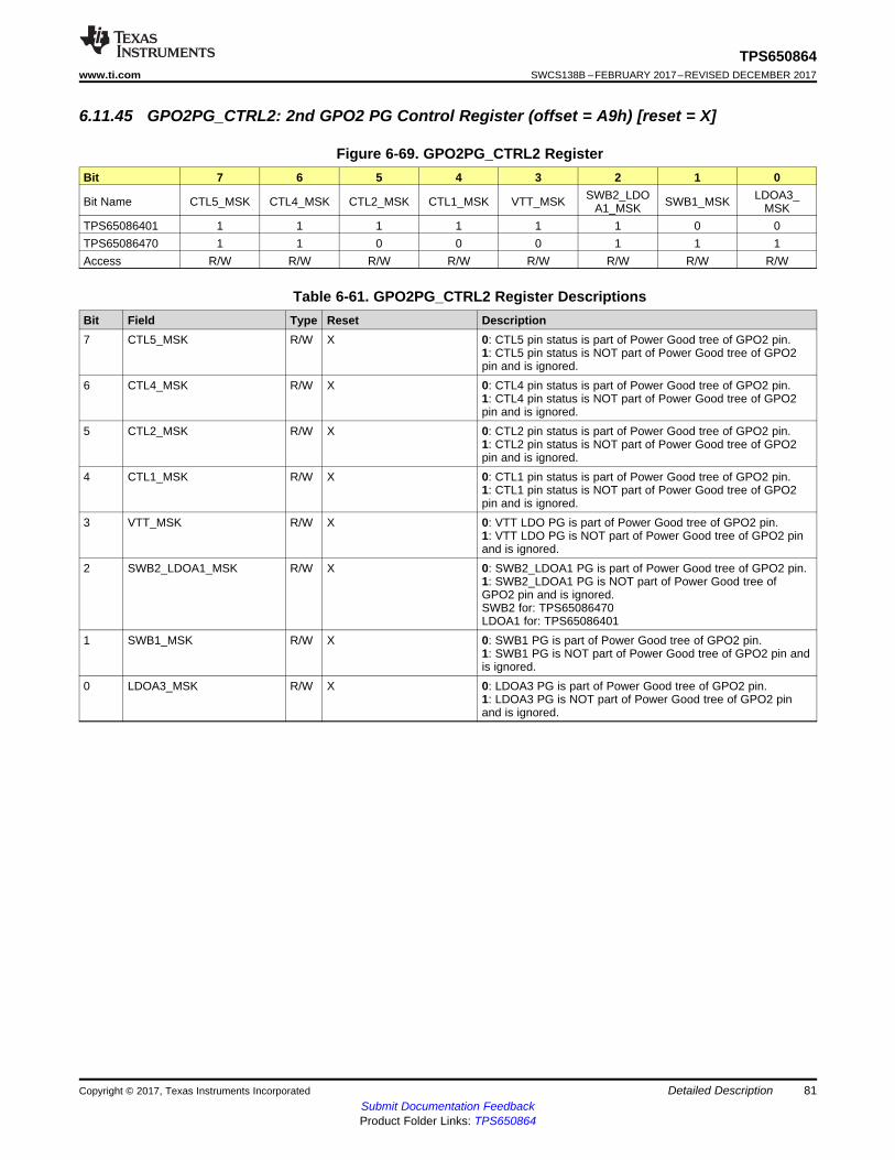
81
TPS650864www.ti.com SWCS138B –FEBRUARY 2017–REVISED DECEMBER 2017
Submit Documentation FeedbackProduct Folder Links: TPS650864
Detailed DescriptionCopyright © 2017, Texas Instruments Incorporated
6.11.45 GPO2PG_CTRL2: 2nd GPO2 PG Control Register (offset = A9h) [reset = X]
Figure 6-69. GPO2PG_CTRL2 RegisterBit 7 6 5 4 3 2 1 0
Bit Name CTL5_MSK CTL4_MSK CTL2_MSK CTL1_MSK VTT_MSK SWB2_LDOA1_MSK SWB1_MSK LDOA3_
MSKTPS65086401 1 1 1 1 1 1 0 0TPS65086470 1 1 0 0 0 1 1 1Access R/W R/W R/W R/W R/W R/W R/W R/W
Table 6-61. GPO2PG_CTRL2 Register DescriptionsBit Field Type Reset Description7 CTL5_MSK R/W X 0: CTL5 pin status is part of Power Good tree of GPO2 pin.
1: CTL5 pin status is NOT part of Power Good tree of GPO2pin and is ignored.
6 CTL4_MSK R/W X 0: CTL4 pin status is part of Power Good tree of GPO2 pin.1: CTL4 pin status is NOT part of Power Good tree of GPO2pin and is ignored.
5 CTL2_MSK R/W X 0: CTL2 pin status is part of Power Good tree of GPO2 pin.1: CTL2 pin status is NOT part of Power Good tree of GPO2pin and is ignored.
4 CTL1_MSK R/W X 0: CTL1 pin status is part of Power Good tree of GPO2 pin.1: CTL1 pin status is NOT part of Power Good tree of GPO2pin and is ignored.
3 VTT_MSK R/W X 0: VTT LDO PG is part of Power Good tree of GPO2 pin.1: VTT LDO PG is NOT part of Power Good tree of GPO2 pinand is ignored.
2 SWB2_LDOA1_MSK R/W X 0: SWB2_LDOA1 PG is part of Power Good tree of GPO2 pin.1: SWB2_LDOA1 PG is NOT part of Power Good tree ofGPO2 pin and is ignored.SWB2 for: TPS65086470LDOA1 for: TPS65086401
1 SWB1_MSK R/W X 0: SWB1 PG is part of Power Good tree of GPO2 pin.1: SWB1 PG is NOT part of Power Good tree of GPO2 pin andis ignored.
0 LDOA3_MSK R/W X 0: LDOA3 PG is part of Power Good tree of GPO2 pin.1: LDOA3 PG is NOT part of Power Good tree of GPO2 pinand is ignored.

82
TPS650864SWCS138B –FEBRUARY 2017–REVISED DECEMBER 2017 www.ti.com
Submit Documentation FeedbackProduct Folder Links: TPS650864
Detailed Description Copyright © 2017, Texas Instruments Incorporated
6.11.46 GPO3PG_CTRL1: 1st GPO3 PG Control Register (offset = AAh) [reset = X]
Figure 6-70. GPO3PG_CTRL1 RegisterBit 7 6 5 4 3 2 1 0
Bit Name LDOA2_MSK
SWA1_MSK
BUCK6_MSK
BUCK5_MSK
BUCK4_MSK
BUCK3_MSK
BUCK2_MSK
BUCK1_MSK
TPS65086401 0 1 0 1 1 1 0 0TPS65086470 1 1 0 1 1 1 1 1Access R/W R/W R/W R/W R/W R/W R/W R/W
Table 6-62. GPO3PG_CTRL1 Register DescriptionsBit Field Type Reset Description7 LDOA2_MSK R/W X 0: LDOA2 PG is part of Power Good tree of GPO3 pin.
1: LDOA2 PG is NOT part of Power Good tree of GPO3 pin andis ignored.
6 SWA1_MSK R/W X 0: SWA1 PG is part of Power Good tree of GPO3 pin.1: SWA1 PG is NOT part of Power Good tree of GPO3 pin andis ignored.
5 BUCK6_MSK R/W X 0: BUCK6 PG is part of Power Good tree of GPO3 pin.1: BUCK6 PG is NOT part of Power Good tree of GPO3 pin andis ignored.
4 BUCK5_MSK R/W X 0: BUCK5 PG is part of Power Good tree of GPO3 pin.1: BUCK5 PG is NOT part of Power Good tree of GPO3 pin andis ignored.
3 BUCK4_MSK R/W X 0: BUCK4 PG is part of Power Good tree of GPO3 pin.1: BUCK4 PG is NOT part of Power Good tree of GPO3 pin andis ignored.
2 BUCK3_MSK R/W X 0: BUCK3 PG is part of Power Good tree of GPO3 pin.1: BUCK3 PG is NOT part of Power Good tree of GPO3 pin andis ignored.
1 BUCK2_MSK R/W X 0: BUCK2 PG is part of Power Good tree of GPO3 pin.1: BUCK2 PG is NOT part of Power Good tree of GPO3 pin andis ignored.
0 BUCK1_MSK R/W X 0: BUCK1 PG is part of Power Good tree of GPO3 pin.1: BUCK1 PG is NOT part of Power Good tree of GPO3 pin andis ignored.

83
TPS650864www.ti.com SWCS138B –FEBRUARY 2017–REVISED DECEMBER 2017
Submit Documentation FeedbackProduct Folder Links: TPS650864
Detailed DescriptionCopyright © 2017, Texas Instruments Incorporated
6.11.47 GPO3PG_CTRL2: 2nd GPO3 PG Control Register (offset = ABh) [reset = X]
Figure 6-71. GPO3PG_CTRL2 RegisterBit 7 6 5 4 3 2 1 0
Bit Name CTL5_MSK CTL4_MSK CTL2_MSK CTL1_MSK VTT_MSK SWB2_LDOA1_MSK SWB1_MSK LDOA3_MSK
TPS65086401 1 1 1 0 1 0 1 1TPS65086470 1 1 0 1 1 1 1 1Access R/W R/W R/W R/W R/W R/W R/W R/W
Table 6-63. GPO3PG_CTRL2 Register DescriptionsBit Field Type Reset Description7 CTL5_MSK R/W X 0: CTL5 pin status is part of Power Good tree of GPO3 pin.
1: CTL5 pin status is NOT part of Power Good tree of GPO3 pinand is ignored.
6 CTL4_MSK R/W X 0: CTL4 pin status is part of Power Good tree of GPO3 pin.1: CTL4 pin status is NOT part of Power Good tree of GPO3 pinand is ignored.
5 CTL2_MSK R/W X 0: CTL2 pin status is part of Power Good tree of GPO3 pin.1: CTL2 pin status is NOT part of Power Good tree of GPO3 pinand is ignored.
4 CTL1_MSK R/W X 0: CTL1 pin status is part of Power Good tree of GPO3 pin.1: CTL1 pin status is NOT part of Power Good tree of GPO3 pinand is ignored.
3 VTT_MSK R/W X 0: VTT LDO PG is part of Power Good tree of GPO3 pin.1: VTT LDO PG is NOT part of Power Good tree of GPO3 pinand is ignored.
2 SWB2_LDOA1_MSK R/W X 0: SWB2_LDOA1 PG is part of Power Good tree of GPO3 pin.1: SWB2_LDOA1 PG is NOT part of Power Good tree of GPO3pin and is ignored.SWB2 for: TPS65086470LDOA1 for: TPS65086401
1 SWB1_MSK R/W X 0: SWB1 PG is part of Power Good tree of GPO3 pin.1: SWB1 PG is NOT part of Power Good tree of GPO3 pin andis ignored.
0 LDOA3_MSK R/W X 0: LDOA3 PG is part of Power Good tree of GPO3 pin.1: LDOA3 PG is NOT part of Power Good tree of GPO3 pin andis ignored.

84
TPS650864SWCS138B –FEBRUARY 2017–REVISED DECEMBER 2017 www.ti.com
Submit Documentation FeedbackProduct Folder Links: TPS650864
Detailed Description Copyright © 2017, Texas Instruments Incorporated
6.11.48 MISCSYSPG Register (offset = ACh) [reset = X]
Figure 6-72. MISCSYSPG RegisterBit 7 6 5 4 3 2 1 0
Bit Name GPO1_CTL3_MSK
GPO1_CTL6_MSK
GPO4_CTL3_MSK
GPO4_CTL6_MSK
GPO2_CTL3_MSK
GPO2_CTL6_MSK
GPO3_CTL3_MSK
GPO3_CTL6_MSK
TPS65086401 1 1 1 1 1 1 1 1TPS65086470 1 1 1 0 1 1 1 1Access R/W R/W R/W R/W R/W R/W R/W R/W
Table 6-64. MISCSYSPG Register DescriptionsBit Field Type Reset Description7 GPO1_CTL3_MSK R/W X 0: CTL3 pin status is part of Power Good tree of GPO1 pin.
1: CTL3 pin status is NOT part of Power Good tree of GPO1 pin.6 GPO1_CTL6_MSK R/W X 0: CTL6 pin status is part of Power Good tree of GPO1 pin.
1: CTL6 pin status is NOT part of Power Good tree of GPO1 pin.5 GPO4_CTL3_MSK R/W X 0: CTL3 pin status is part of Power Good tree of GPO4 pin.
1: CTL3 pin status is NOT part of Power Good tree of GPO4 pin.4 GPO4_CTL6_MSK R/W X 0: CTL6 pin status is part of Power Good tree of GPO4 pin.
1: CTL6 pin status is NOT part of Power Good tree of GPO4 pin.3 GPO2_CTL3_MSK R/W X 0: CTL3 pin status is part of Power Good tree of GPO2 pin.
1: CTL3 pin status is NOT part of Power Good tree of GPO2 pin.2 GPO2_CTL6_MSK R/W X 0: CTL6 pin status is part of Power Good tree of GPO2 pin.
1: CTL6 pin status is NOT part of Power Good tree of GPO2 pin.1 GPO3_CTL3_MSK R/W X 0: CTL3 pin status is part of Power Good tree of GPO3 pin.
1: CTL3 pin status is NOT part of Power Good tree of GPO3pin.0 GPO3_CTL6_MSK R/W X 0: CTL6 pin status is part of Power Good tree of GPO3 pin.
1: CTL6 pin status is NOT part of Power Good tree of GPO3 pin.

85
TPS650864www.ti.com SWCS138B –FEBRUARY 2017–REVISED DECEMBER 2017
Submit Documentation FeedbackProduct Folder Links: TPS650864
Detailed DescriptionCopyright © 2017, Texas Instruments Incorporated
6.11.48.1 VTT_DISCH_CTRL Register (offset = ADh) [reset = X]
Figure 6-73. VTT_DISCH_CTRL RegisterBit 7 6 5 4 3 2 1 0
Bit Name RESERVED RESERVED RESERVED VTT_DISCHG RESERVED RESERVED RESERVED RESERVED
TPS65086401 0 1 0 1 1 1 1 1TPS65086470 0 1 0 1 1 1 0 0Access R/W R/W R/W R/W R/W R/W R/W R/W
Table 6-65. VTT_DISCH_CTRL Register DescriptionsBit Field Type Reset Description7:5 RESERVED R/W X Reserved bits. Always write to match OTP settings.4 VTT_DISCHG R/W X 0: no discharge
1: 100 Ω
3:0 RESERVED R/W X Reserved bits. Always write to match OTP settings.
6.11.49 LDOA1_SWB2_CTRL: LDOA1 and SWB2 Control Register (offset = AEh) [reset = X]
Figure 6-74. LDOA1_SWB2_CTRL RegisterBit 7 6 5 4 3 2 1 0
Bit Name LDOA1_DISCHG[1]
LDOA1_DISCHG[0]
LDOA1_SWB2_SDWN_CONFIG
LDOA1_VID[3]
LDOA1_VID[2]
LDOA1_VID[1]
LDOA1_VID[0]
LDOA1_SWB2_EN
TPS65086401 0 1 0 0 1 0 0 0TPS65086470 0 1 0 0 1 0 0 0Access R/W R/W R/W R/W R/W R/W R/W R/W
Table 6-66. LDOA1_SWB2_CTRL Register DescriptionsBit Field Type Reset Description7:6 LDOA1_DISCHG[1:0] R/W X LDOA1 discharge resistance
00: no discharge01: 100 Ω10: 200 Ω11: 500 Ω
5 LDOA1_SWB2_SDWN_CONFIG
R/W X Control for Disabling LDOA1 or SWB2 (OTP dependent) duringEmergency Shutdown. When LDOA1 is used in sequence andSWB1 and SWB2 are not merged, this will control SWB2.0: LDOA1 or SWB2 will turn off during Emergency Shutdown forfactory-programmable duration of 1 ms, 5 ms, 10 ms, or 100 ms.1: LDOA1 or SWB2 is controlled by LDOA1_SWB2_EN bit only.LDOA1 for: TPS65086470SWB2 for: N/AUnused for TPS65086401
4:1 LDOA1_VID[3:0] R/W X This field sets the LDOA1 regulator output regulation voltage.See Table 6-14 for VOUT options.
0 LDOA1_SWB2_EN R/W X LDOA1 or SWB2 Enable Bit.0: Disable.1: Enable.LDOA1 for TPS65086470SWB2 for N/AUnused for TPS65086401

86
TPS650864SWCS138B –FEBRUARY 2017–REVISED DECEMBER 2017 www.ti.com
Submit Documentation FeedbackProduct Folder Links: TPS650864
Detailed Description Copyright © 2017, Texas Instruments Incorporated
6.11.50 PG_STATUS1: 1st Power Good Status Register (offset = B0h) [reset = 0000 0000]
Figure 6-75. PG_STATUS1 RegisterBit 7 6 5 4 3 2 1 0
Bit Name LDOA2_PGOOD
SWA1_PGOOD
BUCK6_PGOOD
BUCK5_PGOOD
BUCK4_PGOOD
BUCK3_PGOOD
BUCK2_PGOOD
BUCK1_PGOOD
TPS650864xx 0 0 0 0 0 0 0 0Access R R R R R R R R
Table 6-67. PG_STATUS1 Register DescriptionsBit Field Type Reset Description7 LDOA2_PGOOD R 0 LDOA2 Power Good status.
0: The output is not in target regulation range.1: The output is in target regulation range.
6 SWA1_PGOOD R 0 SWA1 Power Good status.0: The output is not in target regulation range.1: The output is in target regulation range.
5 BUCK6_PGOOD R 0 BUCK6 Power Good status.0: The output is not in target regulation range.1: The output is in target regulation range.
4 BUCK5_PGOOD R 0 BUCK5 Power Good status.0: The output is not in target regulation range.1: The output is in target regulation range.
3 BUCK4_PGOOD R 0 BUCK4 Power Good status.0: The output is not in target regulation range.1: The output is in target regulation range.
2 BUCK3_PGOOD R 0 BUCK3 Power Good status.0: The output is not in target regulation range.1: The output is in target regulation range.
1 BUCK2_PGOOD R 0 BUCK2 Power Good status.0: The output is not in target regulation range.1: The output is in target regulation range.
0 BUCK1_PGOOD R 0 BUCK1 Power Good status.0: The output is not in target regulation range.1: The output is in target regulation range.

87
TPS650864www.ti.com SWCS138B –FEBRUARY 2017–REVISED DECEMBER 2017
Submit Documentation FeedbackProduct Folder Links: TPS650864
Detailed DescriptionCopyright © 2017, Texas Instruments Incorporated
6.11.51 PG_STATUS2: 2nd Power Good Status Register (offset = B1h) [reset = 0000 0000]
Figure 6-76. PG_STATUS2 RegisterBit 7 6 5 4 3 2 1 0
Bit Name RESERVED RESERVED LDO5_PGOOD
LDOA1_PGOOD
VTT_PGOOD
SWB2_PGOOD
SWB1_PGOOD
LDOA3_PGOOD
TPS650864xx 0 0 0 0 0 0 0 0Access R R R R R R R R
Table 6-68. PG_STATUS2 Register DescriptionsBit Field Type Reset Description5 LDO5_PGOOD R 0 LDO5 Power Good status.
0: The output is not in target regulation range.1: The output is in target regulation range.
4 LDOA1_PGOOD R 0 LDOA1 Power Good status.0: The output is not in target regulation range.1: The output is in target regulation range.
3 VTT_PGOOD R 0 VTT LDO Power Good status.0: The output is not in target regulation range.1: The output is in target regulation range.
2 SWB2_PGOOD R 0 SWB2 Power Good status.0: The output is not in target regulation range.1: The output is in target regulation range.
1 SWB1_PGOOD R 0 SWB1 Power Good status.0: The output is not in target regulation range.1: The output is in target regulation range.
0 LDOA3_PGOOD R 0 LDOA3 Power Good status.0: The output is not in target regulation range.1: The output is in target regulation range.

88
TPS650864SWCS138B –FEBRUARY 2017–REVISED DECEMBER 2017 www.ti.com
Submit Documentation FeedbackProduct Folder Links: TPS650864
Detailed Description Copyright © 2017, Texas Instruments Incorporated
6.11.52 PWR_FAULT_STATUS1: 1st Power Fault Status Register (offset = B2h) [reset =0000 0000]
Figure 6-77. PWR_FAULT_STATUS1 RegisterBit 7 6 5 4 3 2 1 0
Bit Name LDOA2_PWRFLT
SWA1_PWRFLT
BUCK6_PWRFLT
BUCK5_PWRFLT
BUCK4_PWRFLT
BUCK3_PWRFLT
BUCK2_PWRFLT
BUCK1_PWRFLT
TPS650864xx 0 0 0 0 0 0 0 0Access R/W R/W R/W R/W R/W R/W R/W R/W
Table 6-69. PWR_FAULT_STATUS1 Register DescriptionsBit Field Type Reset Description7 LDOA2_PWRFLT R 0 This fields indicates that LDOA2 has lost its regulation.
0: No Fault.1: Power fault has occurred. The host to write 1 to clear.
6 SWA1_PWRFLT R 0 This fields indicates that SWA1 has lost its regulation.0: No Fault.1: Power fault has occurred. The host to write 1 to clear.
5 BUCK6_PWRFLT R 0 This fields indicates that BUCK6 has lost its regulation.0: No Fault.1: Power fault has occurred. The host to write 1 to clear.
4 BUCK5_PWRFLT R 0 This fields indicates that BUCK5 has lost its regulation.0: No Fault.1: Power fault has occurred. The host to write 1 to clear.
3 BUCK4_PWRFLT R 0 This fields indicates that BUCK4 has lost its regulation.0: No Fault.1: Power fault has occurred. The host to write 1 to clear.
2 BUCK3_PWRFLT R 0 This fields indicates that BUCK3 has lost its regulation.0: No Fault.1: Power fault has occurred. The host to write 1 to clear.
1 BUCK2_PWRFLT R 0 This fields indicates that BUCK2 has lost its regulation.0: No Fault.1: Power fault has occurred. The host to write 1 to clear.
0 BUCK1_PWRFLT R 0 This fields indicates that BUCK1 has lost its regulation.0: No Fault.1: Power fault has occurred. The host to write 1 to clear.

89
TPS650864www.ti.com SWCS138B –FEBRUARY 2017–REVISED DECEMBER 2017
Submit Documentation FeedbackProduct Folder Links: TPS650864
Detailed DescriptionCopyright © 2017, Texas Instruments Incorporated
6.11.53 PWR_FAULT_STATUS2: 2nd Power Fault Status Register (offset = B3h) [reset =0000 0000]
Figure 6-78. PWR_FAULT_STATUS2 RegisterBit 7 6 5 4 3 2 1 0
Bit Name RESERVED RESERVED RESERVED LDOA1_PWRFLT
VTT_PWRFLT
SWB2__PWRFLT
SWB1_PWRFLT
LDOA3_PWRFLT
TPS650864xx 0 0 0 0 0 0 0 0Access R R R/W R/W R/W R/W R/W R/W
Table 6-70. PWR_FAULT_STATUS2 Register DescriptionsBit Field Type Reset Description4 LDOA1_PWRFLT R/W 0 This fields indicates that LDOA1 has lost its regulation.
0: No Fault.1: Power fault has occurred. The host to write 1 to clear.
3 VTT_PWRFLT R/W 0 This fields indicates that VTT LDO has lost its regulation.0: No Fault.1: Power fault has occurred. The host to write 1 to clear.
2 SWB2_PWRFLT R/W 0 This fields indicates that SWB2 has lost its regulation.0: No Fault.1: Power fault has occurred. The host to write 1 to clear.
1 SWB1_PWRFLT R/W 0 This fields indicates that SWB1 has lost its regulation.0: No Fault.1: Power fault has occurred. The host to write 1 to clear.
0 LDOA3_PWRFLT R/W 0 This fields indicates that LDOA3 has lost its regulation.0: No Fault.1: Power fault has occurred. The host to write 1 to clear.
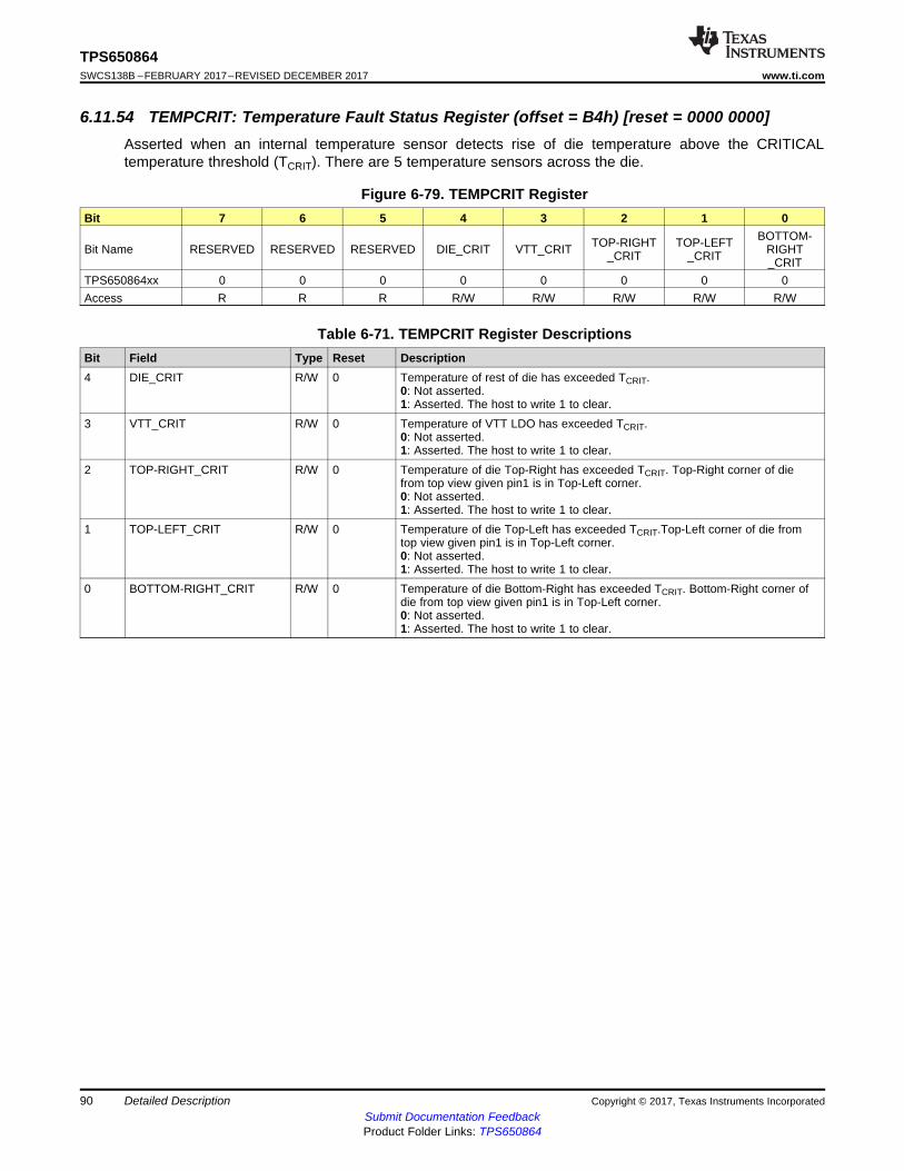
90
TPS650864SWCS138B –FEBRUARY 2017–REVISED DECEMBER 2017 www.ti.com
Submit Documentation FeedbackProduct Folder Links: TPS650864
Detailed Description Copyright © 2017, Texas Instruments Incorporated
6.11.54 TEMPCRIT: Temperature Fault Status Register (offset = B4h) [reset = 0000 0000]Asserted when an internal temperature sensor detects rise of die temperature above the CRITICALtemperature threshold (TCRIT). There are 5 temperature sensors across the die.
Figure 6-79. TEMPCRIT RegisterBit 7 6 5 4 3 2 1 0
Bit Name RESERVED RESERVED RESERVED DIE_CRIT VTT_CRIT TOP-RIGHT_CRIT
TOP-LEFT_CRIT
BOTTOM-RIGHT_CRIT
TPS650864xx 0 0 0 0 0 0 0 0Access R R R R/W R/W R/W R/W R/W
Table 6-71. TEMPCRIT Register DescriptionsBit Field Type Reset Description4 DIE_CRIT R/W 0 Temperature of rest of die has exceeded TCRIT.
0: Not asserted.1: Asserted. The host to write 1 to clear.
3 VTT_CRIT R/W 0 Temperature of VTT LDO has exceeded TCRIT.0: Not asserted.1: Asserted. The host to write 1 to clear.
2 TOP-RIGHT_CRIT R/W 0 Temperature of die Top-Right has exceeded TCRIT. Top-Right corner of diefrom top view given pin1 is in Top-Left corner.0: Not asserted.1: Asserted. The host to write 1 to clear.
1 TOP-LEFT_CRIT R/W 0 Temperature of die Top-Left has exceeded TCRIT.Top-Left corner of die fromtop view given pin1 is in Top-Left corner.0: Not asserted.1: Asserted. The host to write 1 to clear.
0 BOTTOM-RIGHT_CRIT R/W 0 Temperature of die Bottom-Right has exceeded TCRIT. Bottom-Right corner ofdie from top view given pin1 is in Top-Left corner.0: Not asserted.1: Asserted. The host to write 1 to clear.

91
TPS650864www.ti.com SWCS138B –FEBRUARY 2017–REVISED DECEMBER 2017
Submit Documentation FeedbackProduct Folder Links: TPS650864
Detailed DescriptionCopyright © 2017, Texas Instruments Incorporated
6.11.55 TEMPHOT: Temperature Hot Status Register (offset = B5h) [reset = 0000 0000]Asserted when an internal temperature sensor detects rise of die temperature above the HOT temperaturethreshold (THOT). There are 5 temperature sensors across the die.
Figure 6-80. TEMPHOT RegisterBit 7 6 5 4 3 2 1 0
Bit Name RESERVED RESERVED RESERVED DIE_HOT VTT_HOT TOP-RIGHT_HOT
TOP-LEFT_HOT
BOTTOM-RIGHT_HOT
TPS650864xx 0 0 0 0 0 0 0 0Access R R R R/W R/W R/W R/W R/W
Table 6-72. TEMPHOT Register DescriptionsBit Field Type Reset Description4 DIE_HOT R/W 0 Temperature of rest of die has exceeded THOT.
0: Not asserted.1: Asserted. The host to write 1 to clear.
3 VTT_HOT R/W 0 Temperature of VTT LDO has exceeded THOT.0: Not asserted.1: Asserted. The host to write 1 to clear.
2 TOP-RIGHT_HOT R/W 0 Temperature of Top-Right has exceeded THOT. Top-Right corner of die from topview given pin1 is in Top-Left corner.0: Not asserted.1: Asserted. The host to write 1 to clear.
1 TOP-LEFT_HOT R/W 0 Temperature of Top-Left has exceeded THOT. Top-Left corner of die from topview given pin1 is in Top-Left corner.0: Not asserted.1: Asserted. The host to write 1 to clear.
0 BOTTOM-RIGHT_HOT R/W 0 Temperature of Bottom-Right has exceeded THOT. Bottom-Right corner of diefrom top view given pin1 is in Top-Left corner.0: Not asserted.1: Asserted. The host to write 1 to clear.

92
TPS650864SWCS138B –FEBRUARY 2017–REVISED DECEMBER 2017 www.ti.com
Submit Documentation FeedbackProduct Folder Links: TPS650864
Detailed Description Copyright © 2017, Texas Instruments Incorporated
6.11.56 OC_STATUS: Overcurrent Fault Status Register (offset = B6h) [reset = 0000 0000]Asserted when overcurrent condition is detected from a LSD FET.
Figure 6-81. OC_STATUS RegisterBit 7 6 5 4 3 2 1 0
Bit Name RESERVED RESERVED RESERVED RESERVED RESERVED BUCK6_OC
BUCK2_OC
BUCK1_OC
TPS650864xx 0 0 0 0 0 0 0 0Access R R R R R R/W R/W R/W
Table 6-73. OC_STATUS Register DescriptionsBit Field Type Reset Description2 BUCK6_OC R/W 0 BUCK6 LSD FET overcurrent has been detected.
0: Not asserted.1: Asserted. The host to write 1 to clear.
1 BUCK2_OC R/W 0 BUCK2 LSD FET overcurrent has been detected.0: Not asserted.1: Asserted. The host to write 1 to clear.
0 BUCK1_OC R/W 0 BUCK1 LSD FET overcurrent has been detected.0: Not asserted.1: Asserted. The host to write 1 to clear.

93
TPS650864www.ti.com SWCS138B –FEBRUARY 2017–REVISED DECEMBER 2017
Submit Documentation FeedbackProduct Folder Links: TPS650864
Applications, Implementation, and LayoutCopyright © 2017, Texas Instruments Incorporated
7 Applications, Implementation, and Layout
NOTEInformation in the following applications sections is not part of the TI componentspecification, and TI does not warrant its accuracy or completeness. TI’s customers areresponsible for determining suitability of components for their purposes. Customers shouldvalidate and test their design implementation to confirm system functionality.
7.1 Application InformationThe TPS650864xx for Xilinx MPSoCs and FPGAs can be used in a variety of ways which is outlined in thefollowing sections. Section 7.2 discusses the design procedure for the general case. Specific OTPinformation can be found starting with Section 6.4. In general, the PMIC is controlled by the state of the sixCTL which can accept up to 3.6 V inputs. How these control pins are set varies based on application.Some examples would be using the PG of external rails, looping GPOs back into CTL pins, connecting alocking push-button, using a push-button circuit, using an embedded controller (such as theMSP430G2121), or controlled by the MPSoC itself.
7.2 Typical Application
7.2.1 Typical Application ExampleThis section describes the general application information and provides a more detailed description on theTPS650864xx device that powers a generic multicore-processor application. An example system blockdiagram for the device powering an SoC and the rest of platform is shown in Figure 7-1. The functionalblock diagram in Figure 6-1 outlines the typical external components necessary for proper devicefunctionality.

DDR
BUCK1
BUCK2
BUCK3 3A
BUCK4 3A
BUCK5 3A
BUCK6
VTT LDO ±0.5A
LDOA2 0.6A
LDOA3 0.6A
SWA1 0.3A
SWB1 0.3A
SWB2 0.3A
LDO5
LDO3P3
PG_5V
EXT FET
EXT FET
EXT FET
VCORE
VGPU
VCCIO
VCPU1
VCPU2
VDDQ, VDD1&2
VREF, VTT
VSUPP2
VSUPP3
VSUPP4
VSUPP5
PMIC Example SoC PLATFORMVIN
LDO5V
1.8V
5V Supply
VSYS
IRQB
SCL
SDA
GPO1 ± GPO4
VSUPP6
CTL1 ± CTL6
LDOA1 0.2A VSUPP1
Input up to 3.3V
Input up to 3.3V
5V Supply
VIN
VIN
DDR
VDDQ, VDD1&2
VREF, VTT
Note: An LDO or Buck Can Supply the VPP Rail if Needed for DDR.
LDO5V or 5V Supply
VIN
Copyright © 2017, Texas Instruments Incorporated
94
TPS650864SWCS138B –FEBRUARY 2017–REVISED DECEMBER 2017 www.ti.com
Submit Documentation FeedbackProduct Folder Links: TPS650864
Applications, Implementation, and Layout Copyright © 2017, Texas Instruments Incorporated
Figure 7-1. Typical Application Example
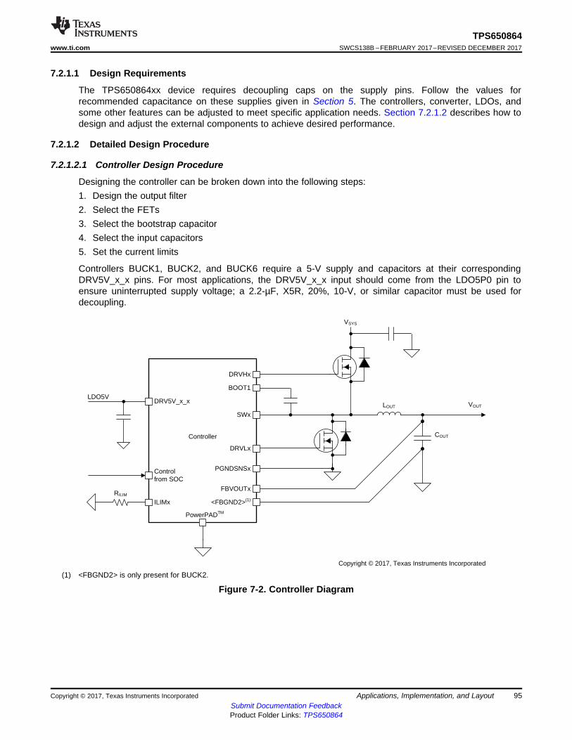
Controller
DRVHx
DRVLx
BOOT1
SWx
FBVOUTx
<FBGND2>(1)
PGNDSNSx
VOUT
VSYS
LOUT
ILIMx
DRV5V_x_xLDO5V
Control from SOC
PowerPADTM
COUT
RILIM
Copyright © 2017, Texas Instruments Incorporated
95
TPS650864www.ti.com SWCS138B –FEBRUARY 2017–REVISED DECEMBER 2017
Submit Documentation FeedbackProduct Folder Links: TPS650864
Applications, Implementation, and LayoutCopyright © 2017, Texas Instruments Incorporated
7.2.1.1 Design Requirements
The TPS650864xx device requires decoupling caps on the supply pins. Follow the values forrecommended capacitance on these supplies given in Section 5. The controllers, converter, LDOs, andsome other features can be adjusted to meet specific application needs. Section 7.2.1.2 describes how todesign and adjust the external components to achieve desired performance.
7.2.1.2 Detailed Design Procedure
7.2.1.2.1 Controller Design Procedure
Designing the controller can be broken down into the following steps:1. Design the output filter2. Select the FETs3. Select the bootstrap capacitor4. Select the input capacitors5. Set the current limits
Controllers BUCK1, BUCK2, and BUCK6 require a 5-V supply and capacitors at their correspondingDRV5V_x_x pins. For most applications, the DRV5V_x_x input should come from the LDO5P0 pin toensure uninterrupted supply voltage; a 2.2-µF, X5R, 20%, 10-V, or similar capacitor must be used fordecoupling.
(1) <FBGND2> is only present for BUCK2.
Figure 7-2. Controller Diagram
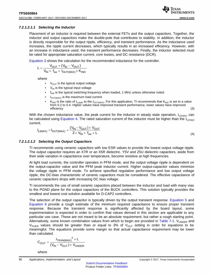
2TRAN(MAX)
OUTIN OUT UNDER
I LC
(V V ) V
u
!
� u
IN OUT OUTL(MAX) OUT(MAX)
IN sw
(V V ) VI I
2 V f L
� u �
u u u
OUT IN OUT
IN sw OUT(MAX) IND
V (V V )L
V f I K
u �
u u u
96
TPS650864SWCS138B –FEBRUARY 2017–REVISED DECEMBER 2017 www.ti.com
Submit Documentation FeedbackProduct Folder Links: TPS650864
Applications, Implementation, and Layout Copyright © 2017, Texas Instruments Incorporated
7.2.1.2.1.1 Selecting the Inductor
Placement of an inductor is required between the external FETs and the output capacitors. Together, theinductor and output capacitors make the double-pole that contributes to stability. In addition, the inductoris directly responsible for the output ripple, efficiency, and transient performance. As the inductance usedincreases, the ripple current decreases, which typically results in an increased efficiency. However, withan increase in inductance used, the transient performance decreases. Finally, the inductor selected mustbe rated for appropriate saturation current, core losses, and DC resistance (DCR).
Equation 3 shows the calculation for the recommended inductance for the controller.
where• VOUT is the typical output voltage• VIN is the typical input voltage• fSW is the typical switching frequency when loaded, 1 MHz unless otherwise noted• IOUT(MAX) is the maximum load current• KIND is the ratio of ILripple to the IOUT(MAX). For this application, TI recommends that KIND is set to a value
from 0.2 to 0.4. Higher values have improved transient performance, lower values have improvedefficiency (3)
With the chosen inductance value, the peak current for the inductor in steady state operation, IL(max), canbe calculated using Equation 4. The rated saturation current of the inductor must be higher than the IL(max)current.
(4)
7.2.1.2.1.2 Selecting the Output Capacitors
TI recommends using ceramic capacitors with low ESR values to provide the lowest output voltage ripple.The output capacitor requires an X7R or an X5R dielectric. Y5V and Z5U dielectric capacitors, aside fromtheir wide variation in capacitance over temperature, become resistive at high frequencies.
At light load currents, the controller operates in PFM mode, and the output voltage ripple is dependent onthe output-capacitor value and the PFM peak inductor current. Higher output-capacitor values minimizethe voltage ripple in PFM mode. To achieve specified regulation performance and low output voltageripple, the DC-bias characteristic of ceramic capacitors must be considered. The effective capacitance ofceramic capacitors drops with increasing DC bias voltage.
TI recommends the use of small ceramic capacitors placed between the inductor and load with many viasto the PGND plane for the output capacitors of the BUCK controllers. This solution typically provides thesmallest and lowest cost solution available for D-CAP2 controllers.
The selection of the output capacitor is typically driven by the output transient response. Equation 5 andEquation 6 provide a rough estimate of the minimum required capacitance to ensure proper transientresponse. Because the transient response is significantly affected by the board layout, someexperimentation is expected in order to confirm that values derived in this section are applicable to anyparticular use case. These are not meant to be an absolute requirement, but rather a rough starting point.Alternatively, some known combination values from which to begin are provided in Table 7-1. VUNDER andVOVER values should be greater than or equal to 3% of VOUT setting in order for equations to bemeaningful. The equations provide some margin so that actual capacitance requirement may be lowerthan calculated.
where
OUTOUT
IN SW
V 50 sC
V f L
u P!
u u
� �2ON_EXT OUT IN OUT
OUT 2IN SW OVER
T V V VC
� 9 ¦ 9 /
u u �!
u u u u
2TRAN(MAX)
OUTOUT OVER
I LC
V V
u
!u
97
TPS650864www.ti.com SWCS138B –FEBRUARY 2017–REVISED DECEMBER 2017
Submit Documentation FeedbackProduct Folder Links: TPS650864
Applications, Implementation, and LayoutCopyright © 2017, Texas Instruments Incorporated
• ITRAN(max) is the maximum load current step• L is the chosen inductance• VIN is the maximum input voltage• VOUT is the minimum programmed output voltage• VUNDER is the maximum allowable undershoot from programmed voltage (5)
where• VOVER is the maximum allowable overshoot from programmed voltage (6)
Another key performance factor can be the ripple voltage while in pulsed frequency modulation mode, alsoknown as discontinuous conduction mode. At light load, the controller will disable the low side FET once itdetects a zero-crossing event on the inductor current. It will stay disabled until VOUT crosses below the setVID threshold. This architecture allows significant power savings at light load conditions by minimizingpower loss through the low side FET and through switching. The disadvantage is that there is highervoltage ripple since the ripple current is only positive. Additionally, for even higher efficiency, TON(PFM) forthis device is typically 80% longer than TON(PWM), which can be calculated by dividing the duty cycle by theswitching frequency. An estimate for the required capacitance for a given allowable ripple voltage at lightload is shown in Equation 7. ESR of the output capacitor is neglected here because ceramic capacitors,which typically have low ESR, are recommended. VOVER should not be set lower than 3% of VOUT value.
where• TON_EXT is the PFM on time extension constant, 1.8 unless otherwise noted in the part number specific
section• VOUT is the maximum programmed output voltage• VIN is the maximum input voltage• fSW is the typical switching frequency when loaded, 1 MHz unless otherwise noted• VOVER is the maximum allowable overshoot from programmed voltage• L is the chosen inductance (7)
In cases where the transient current change is very low and ripple voltage allowance is large, the DCstability may become important. DCAP2 is a very stable architecture so this value is likely to be thesmallest of those calculated. Equation 8 approximates the amount of capacitance necessary to maintainDC stability. Again, this is provided as a starting point; actual values will vary on a board-to-board case.
where• VOUT is the maximum programmed output voltage• 50 µs is based on internal ramp setup• VIN is the minimum input voltage• fSW is the typical switching frequency• L is the chosen inductance (8)
Choosing the maximum valuable between Equation 5, Equation 6, Equation 7, and Equation 8 isrecommended as a starting point to get the desired performance. All equations are estimates and havenot been validated at all variable corners. Removing excess capacitance or adding extra capacitance maybe necessary during board evaluation. Testing can typically be performed on the evaluation module or onprototype boards.

98
TPS650864SWCS138B –FEBRUARY 2017–REVISED DECEMBER 2017 www.ti.com
Submit Documentation FeedbackProduct Folder Links: TPS650864
Applications, Implementation, and Layout Copyright © 2017, Texas Instruments Incorporated
Table 7-1. Known LC Combinations for 1 µs Load Rise and Fall Time
ITRAN(max) (A) L (µH) VOUT (V) VUNDER (V) VOVER (V) COUT(µF)3.5 0.47 1 0.05 0.05 1104 0.47 1 0.05 0.05 2205 0.47 1.35 0.068 0.068 2208 0.33 1 0.05 0.06 44020 0.22 1 0.05 0.16 550
7.2.1.2.1.3 Selecting the FETs
This controller is designed to drive two NMOS FETs. Typically, lower RDSON values are better forimproving the overall efficiency of the controller, however higher gate charge thresholds will result in lowerefficiency so the two need to be balanced for optimal performance. As the RDSON for the low-side FETdecreases, the minimum current limit increases; therefore, ensure selection of the appropriate values forthe FETs, inductor, output capacitors, and current limit resistor. TI's CSD85301Q2, CSD87331Q3D,CSD87381P, CSD87588N, and CSD87350Q5D devices are recommended for the controllers, dependingon the required maximum current.
7.2.1.2.1.4 Bootstrap Capacitor
To ensure the internal high-side gate drivers are supplied with a stable low-noise supply voltage, acapacitor must be connected between the SWx pins and the respective BOOTx pins. TI recommendsplacing ceramic capacitors with the value of 0.1 µF for the controllers. During testing, a 0.1-µF, size 0402,10-V capacitor is used for the controllers.
TI recommends reserving a small resistor in series with the bootstrap capacitor in case the turnon andturnoff of the FETs must be slowed to reduce voltage ringing on the switch node, which is a commonpractice for controller design.
7.2.1.2.1.5 Setting the Current Limit
The current-limiting resistor value must be chosen based on Equation 1.
7.2.1.2.1.6 Selecting the Input Capacitors
Due to the nature of the switching controller with a pulsating input current, a low ESR input capacitor isrequired for best input-voltage filtering and also for minimizing the interference with other circuits causedby high input-voltage spikes. For the controller, a typical 2.2-µF capacitor can be used for the DRV5V_x_xpin to handle the transients on the driver. For the FET input, 10 µF of input capacitance (after derating) isrecommended for most applications. To achieve the low ESR requirement, a ceramic capacitor isrecommended. However, the voltage rating and DC-bias characteristic of ceramic capacitors must beconsidered. For better input-voltage filtering, the input capacitor can be increased without any limit.
NOTEUse the correct value for the ceramic capacitor capacitance after derating to achieve therecommended input capacitance.
TI recommends placing a ceramic capacitor as close as possible to the FET across the respective VSYSand PGND pins of the FETs. The preferred capacitors for the controllers are two MurataGRM21BR61E226ME44: 22-µF, 0805, 25-V, ±20%, or similar capacitors.
7.2.1.2.2 Converter Design Procedure
Designing the converter has only two steps: design the output filter and select the input capacitors.
Figure 7-3 shows a diagram of the converter.

Converter
LXx
FBx
Pow
erPA
DT
M
PVINx
Control from SOC
CIN
VIN_BUCK345_ANA VOUTLOUT
Copyright © 2017, Texas Instruments Incorporated
99
TPS650864www.ti.com SWCS138B –FEBRUARY 2017–REVISED DECEMBER 2017
Submit Documentation FeedbackProduct Folder Links: TPS650864
Applications, Implementation, and LayoutCopyright © 2017, Texas Instruments Incorporated
Figure 7-3. Converter Diagram
7.2.1.2.2.1 Selecting the Inductor
Internal parameters for the converters are optimized for either a 0.47 µH or 1 µH inductor, however it ispossible to use other inductor values as long as they are chosen carefully and thoroughly tested. Theequations from Section 7.2.1.2.1.1 can be utilized again with the parameters changed to match those ofthe converters. Switching frequency estimates can be found in Section 5.15.
7.2.1.2.2.2 Selecting the Output Capacitors
Ceramic capacitors with low ESR values are recommended because they provide the lowest outputvoltage ripple. The output capacitor requires either an X7R or X5R rating. Y5V and Z5U capacitors, asidefrom the wide variation in capacitance over temperature, become resistive at high frequencies.
At light load currents, the converter operates in PFM mode and the output voltage ripple is dependent onthe output-capacitor value and the PFM peak inductor current. Higher output-capacitor values minimizethe voltage ripple in PFM mode. To achieve specified regulation performance and low output voltageripple, the DC-bias characteristic of ceramic capacitors must be considered. The effective capacitance ofceramic capacitors drops with increasing DC-bias voltage.
For the output capacitors of the BUCK converters, TI recommends placing small ceramic capacitorsbetween the inductor and load with many vias to the PGND plane. This solution typically provides thesmallest and lowest-cost solution available.
The minimum output capacitance recommended is 22 µF for stability. Equation 5 and Equation 6 can beused to estimate the required output capacitance for a given load transient. Note that VIN will be differentfor the converters and that the switching frequency can be estimated using Section 5.15. Equation 7 canbe neglected for converters as there is no on time extension and the VIN - VOUT term is typically smaller.
7.2.1.2.2.3 Selecting the Input Capacitors
Due to the nature of the switching converter with a pulsating input current, a low ESR input capacitor isrequired for best input-voltage filtering and for minimizing the interference with other circuits caused byhigh input-voltage spikes. For the PVINx pin, 2.5 µF of input capacitance (after derating) is required formost applications. A ceramic capacitor is recommended to achieve the low ESR requirement. However,the voltage rating and DC-bias characteristic of ceramic capacitors must be considered. The inputcapacitor can be increased without any limit for better input-voltage filtering.

100
TPS650864SWCS138B –FEBRUARY 2017–REVISED DECEMBER 2017 www.ti.com
Submit Documentation FeedbackProduct Folder Links: TPS650864
Applications, Implementation, and Layout Copyright © 2017, Texas Instruments Incorporated
NOTEUse the correct value for the ceramic capacitor capacitance after derating to achieve therecommended input capacitance.
The preferred capacitor for the converters is one Samsung CL05A106MP5NUNC: 10-µF, 0402, 10-V,±20%, or similar capacitor.
7.2.1.2.3 LDO Design Procedure
The VTT LDO must handle the fast load transients from the DDR memory for termination. Therefore, it isrecommended to use ceramic capacitors to maintain a high amount of capacitance with low ESR on theVTT LDO outputs and inputs. The preferred output capacitors for the VTT LDO are theGRM188R60J226MEA0 from Murata (22 µF, 0603, 6.3 V, ±20%, or similar capacitors). The preferredinput capacitor for the VTT LDO is the CL05A106MP5NUNC from Samsung (10-µF, 0402, 10-V, ±20%, orsimilar capacitor).
The remaining LDOs must have input and output capacitors chosen based on the values in Section 5.9.
7.2.1.3 Application Curves
FET = CSD87588N L = PIMB062D-R22MSCOUT = 2 × 300 µF + 1 × 22 µF
Figure 7-4. BUCK2 Controller Load Transient
L = PIFE32251B-R47MS COUT = 4 × 22 µF
Figure 7-5. BUCK3 Converter Load Transient
7.2.1.4 Layout
7.2.1.4.1 Layout Guidelines
For a detailed description regarding layout recommendations, refer to the TPS65086x Design Guide andto the TPS65086x Schematic and Layout Checklist. For all switching power supplies, the layout is animportant step in the design, especially at high peak currents and high switching frequencies. If the layoutis not carefully done, the regulator can have stability problems and EMI issues. Therefore, use wide andshort traces for the main current path and for the power ground tracks. The input capacitors, outputcapacitors, and inductors must be placed as close as possible to the device. Use a common-ground nodefor power ground and use a different, isolated node for control ground to minimize the effects of groundnoise. Connect these ground nodes close to the AGND pin by one or two vias. Use of the design guide ishighly encouraged in addition to the following list of other basic requirements:

BUCK2
BUCK3 BUCK5 BUCK4 BUCK1
BUCK6VTTVREF Capacitor
101
TPS650864www.ti.com SWCS138B –FEBRUARY 2017–REVISED DECEMBER 2017
Submit Documentation FeedbackProduct Folder Links: TPS650864
Applications, Implementation, and LayoutCopyright © 2017, Texas Instruments Incorporated
• Do not allow the AGND, PGNDSNSx, or FBGND2 to connect to the thermal pad on the top layer.• To ensure proper sensing based on FET RDSON, PGNDSNSx must not connect to PGND until very
close to the PGND pin of the FET.• All inductors, input and output capacitors, and FETs for the converters and controller must be on the
same board layer as the IC.• To achieve the best regulation performance, place feedback connection points near the output
capacitors and minimize the control feedback loop as much as possible.• Bootstrap capacitors must be placed close to the device.• The internal reference regulators must have their input and output capacitors placed close to the
device pins.• Route DRVHx and SWx as a differential pair. Ensure that there is a PGND path routed in parallel with
DRVLx, which provides optimal driver loops.
7.2.1.4.2 Layout Example
Figure 7-6. EVM Layout Example With All Components on the Top Layer
DDR
BUCK1
BUCK2
BUCK3 3.5A
BUCK4 3A
BUCK5 3A
BUCK6
VTT LDO ±0.5A
LDOA2 0.6A
LDOA3 0.6A
SWA1 0.3A
SWB1 0.3A
SWB2 0.3A
LDO5
LDO3P3
PG_5V
EXT FET
EXT FET
EXT FET
VCORE
VGPU
VCCIO
VCPU1
VCPU2
VDDQ, VDD1&2
VREF, VTT
VSUPP2
VSUPP3
VSUPP4
VSUPP5
PMIC Example SoC PLATFORMVIN
LDO5V
1.8V
5V Supply
VSYS
IRQB
SCLK
DATA
GPO1
GPO2
GPO3
GPO4
VSUPP6
CTL1
CTL2
CTL3
CTL4
CTL5
CTL6
LDOA1 0.2A VSUPP1
Input up to 3.3V
Input up to 3.3V
5V
Charge Pump or Boost
VSYS = Vout - Vf
40 mA ± 440 mA
VIN
VIN
VIN
DDR
VDDQ, VDD1&2
VREF, VTT
Note: An LDO or Buck Can Supply the VPP Rail if Needed for DDR.
5 V
Supply Diode Needed if Pre-bias is Not Supported
LDO5V or 5V Supply
Copyright © 2017, Texas Instruments Incorporated
102
TPS650864SWCS138B –FEBRUARY 2017–REVISED DECEMBER 2017 www.ti.com
Submit Documentation FeedbackProduct Folder Links: TPS650864
Applications, Implementation, and Layout Copyright © 2017, Texas Instruments Incorporated
7.2.2 VIN 5-V ApplicationThe PMIC can be operated by a 5-V input voltage to the system because the power path of the controllerdoes not go through the device itself. The concept is simple: supply the controller VINs with the 5-V input,and supply the VSYS with a 5.8-V step-up of the 5 V with a boost or charge pump. The 5.8 V isrecommended because the UVLO of the internal LDO5 is at 5.6 V and the device measures the voltage atVSYS and determines the optimum internal compensation and controller settings thus, it is ideal the VSYSbe close to the VIN of the controllers.
Figure 7-7. VIN 5-V Application
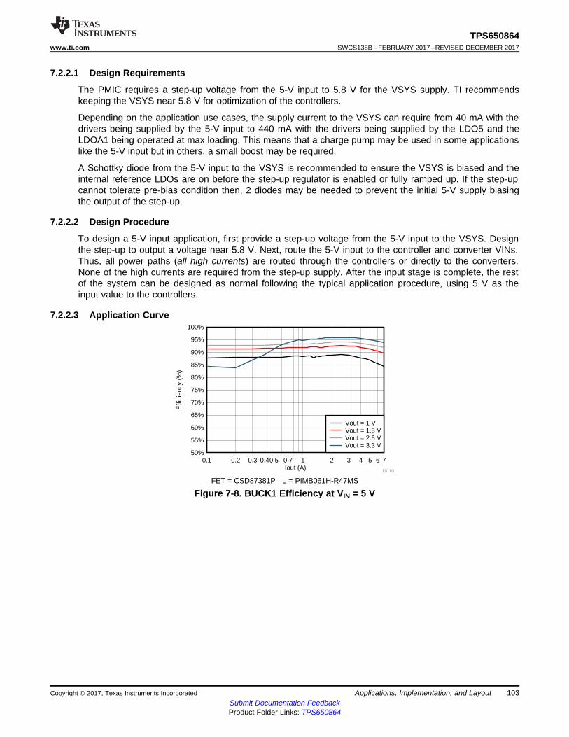
Iout (A)
Effi
cien
cy (
%)
0.1 0.2 0.3 0.40.5 0.7 1 2 3 4 5 6 750%
55%
60%
65%
70%
75%
80%
85%
90%
95%
100%
D010
Vout = 1 VVout = 1.8 VVout = 2.5 VVout = 3.3 V
103
TPS650864www.ti.com SWCS138B –FEBRUARY 2017–REVISED DECEMBER 2017
Submit Documentation FeedbackProduct Folder Links: TPS650864
Applications, Implementation, and LayoutCopyright © 2017, Texas Instruments Incorporated
7.2.2.1 Design Requirements
The PMIC requires a step-up voltage from the 5-V input to 5.8 V for the VSYS supply. TI recommendskeeping the VSYS near 5.8 V for optimization of the controllers.
Depending on the application use cases, the supply current to the VSYS can require from 40 mA with thedrivers being supplied by the 5-V input to 440 mA with the drivers being supplied by the LDO5 and theLDOA1 being operated at max loading. This means that a charge pump may be used in some applicationslike the 5-V input but in others, a small boost may be required.
A Schottky diode from the 5-V input to the VSYS is recommended to ensure the VSYS is biased and theinternal reference LDOs are on before the step-up regulator is enabled or fully ramped up. If the step-upcannot tolerate pre-bias condition then, 2 diodes may be needed to prevent the initial 5-V supply biasingthe output of the step-up.
7.2.2.2 Design Procedure
To design a 5-V input application, first provide a step-up voltage from the 5-V input to the VSYS. Designthe step-up to output a voltage near 5.8 V. Next, route the 5-V input to the controller and converter VINs.Thus, all power paths (all high currents) are routed through the controllers or directly to the converters.None of the high currents are required from the step-up supply. After the input stage is complete, the restof the system can be designed as normal following the typical application procedure, using 5 V as theinput value to the controllers.
7.2.2.3 Application Curve
FET = CSD87381P L = PIMB061H-R47MS
Figure 7-8. BUCK1 Efficiency at VIN = 5 V

104
TPS650864SWCS138B –FEBRUARY 2017–REVISED DECEMBER 2017 www.ti.com
Submit Documentation FeedbackProduct Folder Links: TPS650864
Applications, Implementation, and Layout Copyright © 2017, Texas Instruments Incorporated
7.3 Power Supply Coupling and Bulk CapacitorsThis device is designed to work with several different input voltages. The minimum voltage on the VSYSpin is 5.6 V for the device to start up; however, this is a low power rail. The input to the FETs must befrom 4.5 V to 21 V as long as the proper BOM choices are made. Input to the converters should bebetween 3.3 V and 5 V. For the device to output maximum power, the input power must be sufficient. Forthe controllers, VIN must be able to supply sufficient input current for the output power of the application.For the converters, PVINx must be able to typically supply 2 A.
A best practice here is to determine power usage by the system and back-calculate the necessary powerinput based on expected efficiency values.
7.4 Do's and Don'ts• Connect the LDO5V output to the DRV5V_x_x inputs for situations where an external 5-V supply is not
initially available or is not available the entire time PMIC is on. If the external 5-V supply is alwayspresent, then DRV5V_x_x can be directly connected to remove the V5ANA-to-LDO5P0 load switchRDSON.
• Ensure that none of the control pins are potentially floating.• Include 0-Ω resistors on the DRVH or BOOT pins of controllers on prototype boards, which allows for
slowing the controllers if the system is unable to handle the noise generated by the large switching or ifswitching voltage is too large due to layout.
• Do not connect the V5ANA power input to a different source other than PVINx. A mismatch herecauses reference circuits to regulate incorrectly.
• Do not supply the V5ANA power input before the VSYS. Reference biasing of the internal FETs mayturn on the HS FET passing the input to the output until VSYS is biased.
• Do not change the values of the reserved bits when writing I2C. This can have unexpectedconsequences. Expected values for each OTP are shown in the register map.

105
TPS650864www.ti.com SWCS138B –FEBRUARY 2017–REVISED DECEMBER 2017
Submit Documentation FeedbackProduct Folder Links: TPS650864
Device and Documentation SupportCopyright © 2017, Texas Instruments Incorporated
8 Device and Documentation Support
8.1 Device Support
8.1.1 Development SupportFor documentation related to device development see the following:• Texas Instruments, TPS65086x Schematic and Layout Checklist• Texas Instruments, TPS65086x Design Guide
8.2 Documentation Support
8.2.1 Related DocumentationFor related documentation see the following:• Texas Instruments, CSD85301Q2 20 V Dual N-Channel NexFET™ Power MOSFETs data sheet• Texas Instruments, CSD87331Q3D Synchronous Buck NexFET™ Power Block data sheet• Texas Instruments, CSD87588N Synchronous Buck NexFET™ Power Block II data sheet• Texas Instruments, CSD87381P Synchronous Buck NexFET™ Power Block II data sheet• Texas Instruments, CSD87350Q5D Synchronous Buck NexFET™ Power Block data sheet• Texas Instruments, MSP430G2121 Mixed Signal Microcontroller data sheet• Texas Instruments, Power management integrated buck controllers for distant point-of-load
applications white paper• Texas Instruments, TPS65086x Evaluation Module user's guide
8.3 Receiving Notification of Documentation UpdatesTo receive notification of documentation updates, navigate to the device product folder on ti.com. In theupper right corner, click on Alert me to register and receive a weekly digest of any product information thathas changed. For change details, review the revision history included in any revised document.
8.4 Community ResourcesThe following links connect to TI community resources. Linked contents are provided "AS IS" by therespective contributors. They do not constitute TI specifications and do not necessarily reflect TI's views;see TI's Terms of Use.TI E2E™ Online Community The TI engineer-to-engineer (E2E) community was created to foster
collaboration among engineers. At e2e.ti.com, you can ask questions, share knowledge,explore ideas and help solve problems with fellow engineers.
Design Support TI's Design Support Quickly find helpful E2E forums along with design support toolsand contact information for technical support.
8.5 TrademarksD-CAP2, D-CAP, NexFET, E2E are trademarks of Texas Instruments.NXP is a trademark of NXP Semiconductors.Xilinx, Zynq are registered trademarks of Xilinx.All other trademarks are the property of their respective owners.
106
TPS650864SWCS138B –FEBRUARY 2017–REVISED DECEMBER 2017 www.ti.com
Submit Documentation FeedbackProduct Folder Links: TPS650864
Mechanical, Packaging, and Orderable Information Copyright © 2017, Texas Instruments Incorporated
8.6 Electrostatic Discharge CautionThis integrated circuit can be damaged by ESD. Texas Instruments recommends that all integrated circuits be handled withappropriate precautions. Failure to observe proper handling and installation procedures can cause damage.
ESD damage can range from subtle performance degradation to complete device failure. Precision integrated circuits may be moresusceptible to damage because very small parametric changes could cause the device not to meet its published specifications.
8.7 GlossaryTI Glossary This glossary lists and explains terms, acronyms, and definitions.
9 Mechanical, Packaging, and Orderable Information
The following pages include mechanical, packaging, and orderable information. This information is themost current data available for the designated devices. This data is subject to change without notice andrevision of this document. For browser-based versions of this data sheet, refer to the left-hand navigation.

PACKAGE OPTION ADDENDUM
www.ti.com 14-Dec-2017
Addendum-Page 1
PACKAGING INFORMATION
Orderable Device Status(1)
Package Type PackageDrawing
Pins PackageQty
Eco Plan(2)
Lead/Ball Finish(6)
MSL Peak Temp(3)
Op Temp (°C) Device Marking(4/5)
Samples
TPS65086401RSKR ACTIVE VQFN RSK 64 2000 Green (RoHS& no Sb/Br)
CU NIPDAU Level-3-260C-168 HR -40 to 85 T65086401PG1.0
TPS65086401RSKT ACTIVE VQFN RSK 64 250 Green (RoHS& no Sb/Br)
CU NIPDAU Level-3-260C-168 HR -40 to 85 T65086401PG1.0
TPS65086470RSKR ACTIVE VQFN RSK 64 2000 Green (RoHS& no Sb/Br)
CU NIPDAU Level-3-260C-168 HR -40 to 85 T65086470PG1.0
TPS65086470RSKT ACTIVE VQFN RSK 64 250 Green (RoHS& no Sb/Br)
CU NIPDAU Level-3-260C-168 HR -40 to 85 T65086470PG1.0
(1) The marketing status values are defined as follows:ACTIVE: Product device recommended for new designs.LIFEBUY: TI has announced that the device will be discontinued, and a lifetime-buy period is in effect.NRND: Not recommended for new designs. Device is in production to support existing customers, but TI does not recommend using this part in a new design.PREVIEW: Device has been announced but is not in production. Samples may or may not be available.OBSOLETE: TI has discontinued the production of the device.
(2) RoHS: TI defines "RoHS" to mean semiconductor products that are compliant with the current EU RoHS requirements for all 10 RoHS substances, including the requirement that RoHS substancedo not exceed 0.1% by weight in homogeneous materials. Where designed to be soldered at high temperatures, "RoHS" products are suitable for use in specified lead-free processes. TI mayreference these types of products as "Pb-Free".RoHS Exempt: TI defines "RoHS Exempt" to mean products that contain lead but are compliant with EU RoHS pursuant to a specific EU RoHS exemption.Green: TI defines "Green" to mean the content of Chlorine (Cl) and Bromine (Br) based flame retardants meet JS709B low halogen requirements of <=1000ppm threshold. Antimony trioxide basedflame retardants must also meet the <=1000ppm threshold requirement.
(3) MSL, Peak Temp. - The Moisture Sensitivity Level rating according to the JEDEC industry standard classifications, and peak solder temperature.
(4) There may be additional marking, which relates to the logo, the lot trace code information, or the environmental category on the device.
(5) Multiple Device Markings will be inside parentheses. Only one Device Marking contained in parentheses and separated by a "~" will appear on a device. If a line is indented then it is a continuationof the previous line and the two combined represent the entire Device Marking for that device.
(6) Lead/Ball Finish - Orderable Devices may have multiple material finish options. Finish options are separated by a vertical ruled line. Lead/Ball Finish values may wrap to two lines if the finishvalue exceeds the maximum column width.
Important Information and Disclaimer:The information provided on this page represents TI's knowledge and belief as of the date that it is provided. TI bases its knowledge and belief on informationprovided by third parties, and makes no representation or warranty as to the accuracy of such information. Efforts are underway to better integrate information from third parties. TI has taken and
PACKAGE OPTION ADDENDUM
www.ti.com 14-Dec-2017
Addendum-Page 2
continues to take reasonable steps to provide representative and accurate information but may not have conducted destructive testing or chemical analysis on incoming materials and chemicals.TI and TI suppliers consider certain information to be proprietary, and thus CAS numbers and other limited information may not be available for release.
In no event shall TI's liability arising out of such information exceed the total purchase price of the TI part(s) at issue in this document sold by TI to Customer on an annual basis.

TAPE AND REEL INFORMATION
*All dimensions are nominal
Device PackageType
PackageDrawing
Pins SPQ ReelDiameter
(mm)
ReelWidth
W1 (mm)
A0(mm)
B0(mm)
K0(mm)
P1(mm)
W(mm)
Pin1Quadrant
TPS65086401RSKR VQFN RSK 64 2000 330.0 16.4 8.3 8.3 1.1 12.0 16.0 Q2
TPS65086401RSKT VQFN RSK 64 250 180.0 16.4 8.3 8.3 1.1 12.0 16.0 Q2
TPS65086470RSKR VQFN RSK 64 2000 330.0 16.4 8.3 8.3 1.1 12.0 16.0 Q2
TPS65086470RSKT VQFN RSK 64 250 180.0 16.4 8.3 8.3 1.1 12.0 16.0 Q2
PACKAGE MATERIALS INFORMATION
www.ti.com 14-Dec-2017
Pack Materials-Page 1
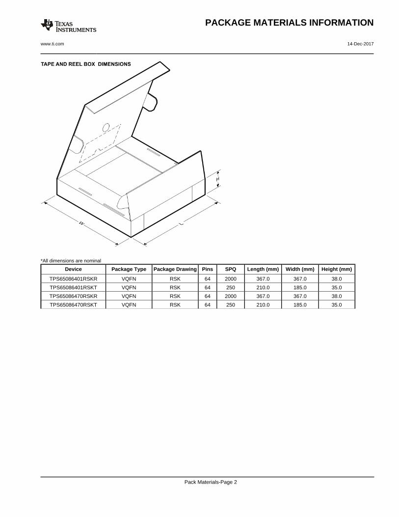
*All dimensions are nominal
Device Package Type Package Drawing Pins SPQ Length (mm) Width (mm) Height (mm)
TPS65086401RSKR VQFN RSK 64 2000 367.0 367.0 38.0
TPS65086401RSKT VQFN RSK 64 250 210.0 185.0 35.0
TPS65086470RSKR VQFN RSK 64 2000 367.0 367.0 38.0
TPS65086470RSKT VQFN RSK 64 250 210.0 185.0 35.0
PACKAGE MATERIALS INFORMATION
www.ti.com 14-Dec-2017
Pack Materials-Page 2
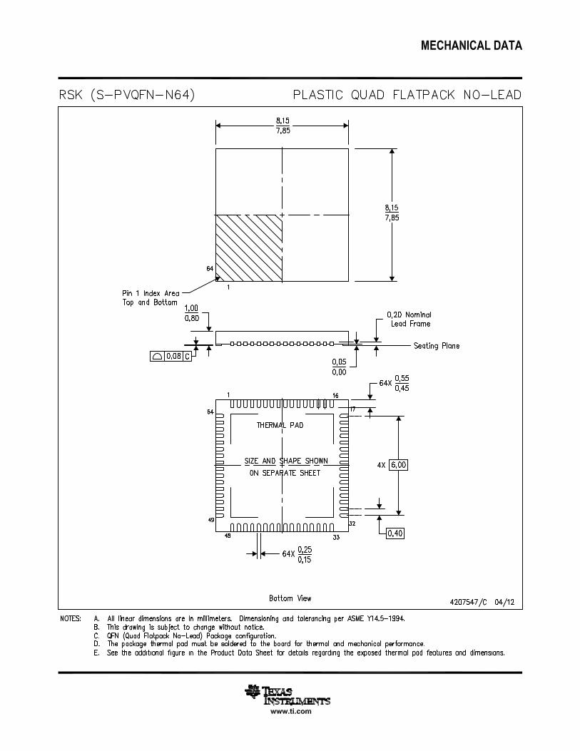


IMPORTANT NOTICE
Texas Instruments Incorporated (TI) reserves the right to make corrections, enhancements, improvements and other changes to itssemiconductor products and services per JESD46, latest issue, and to discontinue any product or service per JESD48, latest issue. Buyersshould obtain the latest relevant information before placing orders and should verify that such information is current and complete.TI’s published terms of sale for semiconductor products (http://www.ti.com/sc/docs/stdterms.htm) apply to the sale of packaged integratedcircuit products that TI has qualified and released to market. Additional terms may apply to the use or sale of other types of TI products andservices.Reproduction of significant portions of TI information in TI data sheets is permissible only if reproduction is without alteration and isaccompanied by all associated warranties, conditions, limitations, and notices. TI is not responsible or liable for such reproduceddocumentation. Information of third parties may be subject to additional restrictions. Resale of TI products or services with statementsdifferent from or beyond the parameters stated by TI for that product or service voids all express and any implied warranties for theassociated TI product or service and is an unfair and deceptive business practice. TI is not responsible or liable for any such statements.Buyers and others who are developing systems that incorporate TI products (collectively, “Designers”) understand and agree that Designersremain responsible for using their independent analysis, evaluation and judgment in designing their applications and that Designers havefull and exclusive responsibility to assure the safety of Designers' applications and compliance of their applications (and of all TI productsused in or for Designers’ applications) with all applicable regulations, laws and other applicable requirements. Designer represents that, withrespect to their applications, Designer has all the necessary expertise to create and implement safeguards that (1) anticipate dangerousconsequences of failures, (2) monitor failures and their consequences, and (3) lessen the likelihood of failures that might cause harm andtake appropriate actions. Designer agrees that prior to using or distributing any applications that include TI products, Designer willthoroughly test such applications and the functionality of such TI products as used in such applications.TI’s provision of technical, application or other design advice, quality characterization, reliability data or other services or information,including, but not limited to, reference designs and materials relating to evaluation modules, (collectively, “TI Resources”) are intended toassist designers who are developing applications that incorporate TI products; by downloading, accessing or using TI Resources in anyway, Designer (individually or, if Designer is acting on behalf of a company, Designer’s company) agrees to use any particular TI Resourcesolely for this purpose and subject to the terms of this Notice.TI’s provision of TI Resources does not expand or otherwise alter TI’s applicable published warranties or warranty disclaimers for TIproducts, and no additional obligations or liabilities arise from TI providing such TI Resources. TI reserves the right to make corrections,enhancements, improvements and other changes to its TI Resources. TI has not conducted any testing other than that specificallydescribed in the published documentation for a particular TI Resource.Designer is authorized to use, copy and modify any individual TI Resource only in connection with the development of applications thatinclude the TI product(s) identified in such TI Resource. NO OTHER LICENSE, EXPRESS OR IMPLIED, BY ESTOPPEL OR OTHERWISETO ANY OTHER TI INTELLECTUAL PROPERTY RIGHT, AND NO LICENSE TO ANY TECHNOLOGY OR INTELLECTUAL PROPERTYRIGHT OF TI OR ANY THIRD PARTY IS GRANTED HEREIN, including but not limited to any patent right, copyright, mask work right, orother intellectual property right relating to any combination, machine, or process in which TI products or services are used. Informationregarding or referencing third-party products or services does not constitute a license to use such products or services, or a warranty orendorsement thereof. Use of TI Resources may require a license from a third party under the patents or other intellectual property of thethird party, or a license from TI under the patents or other intellectual property of TI.TI RESOURCES ARE PROVIDED “AS IS” AND WITH ALL FAULTS. TI DISCLAIMS ALL OTHER WARRANTIES ORREPRESENTATIONS, EXPRESS OR IMPLIED, REGARDING RESOURCES OR USE THEREOF, INCLUDING BUT NOT LIMITED TOACCURACY OR COMPLETENESS, TITLE, ANY EPIDEMIC FAILURE WARRANTY AND ANY IMPLIED WARRANTIES OFMERCHANTABILITY, FITNESS FOR A PARTICULAR PURPOSE, AND NON-INFRINGEMENT OF ANY THIRD PARTY INTELLECTUALPROPERTY RIGHTS. TI SHALL NOT BE LIABLE FOR AND SHALL NOT DEFEND OR INDEMNIFY DESIGNER AGAINST ANY CLAIM,INCLUDING BUT NOT LIMITED TO ANY INFRINGEMENT CLAIM THAT RELATES TO OR IS BASED ON ANY COMBINATION OFPRODUCTS EVEN IF DESCRIBED IN TI RESOURCES OR OTHERWISE. IN NO EVENT SHALL TI BE LIABLE FOR ANY ACTUAL,DIRECT, SPECIAL, COLLATERAL, INDIRECT, PUNITIVE, INCIDENTAL, CONSEQUENTIAL OR EXEMPLARY DAMAGES INCONNECTION WITH OR ARISING OUT OF TI RESOURCES OR USE THEREOF, AND REGARDLESS OF WHETHER TI HAS BEENADVISED OF THE POSSIBILITY OF SUCH DAMAGES.Unless TI has explicitly designated an individual product as meeting the requirements of a particular industry standard (e.g., ISO/TS 16949and ISO 26262), TI is not responsible for any failure to meet such industry standard requirements.Where TI specifically promotes products as facilitating functional safety or as compliant with industry functional safety standards, suchproducts are intended to help enable customers to design and create their own applications that meet applicable functional safety standardsand requirements. Using products in an application does not by itself establish any safety features in the application. Designers mustensure compliance with safety-related requirements and standards applicable to their applications. Designer may not use any TI products inlife-critical medical equipment unless authorized officers of the parties have executed a special contract specifically governing such use.Life-critical medical equipment is medical equipment where failure of such equipment would cause serious bodily injury or death (e.g., lifesupport, pacemakers, defibrillators, heart pumps, neurostimulators, and implantables). Such equipment includes, without limitation, allmedical devices identified by the U.S. Food and Drug Administration as Class III devices and equivalent classifications outside the U.S.TI may expressly designate certain products as completing a particular qualification (e.g., Q100, Military Grade, or Enhanced Product).Designers agree that it has the necessary expertise to select the product with the appropriate qualification designation for their applicationsand that proper product selection is at Designers’ own risk. Designers are solely responsible for compliance with all legal and regulatoryrequirements in connection with such selection.Designer will fully indemnify TI and its representatives against any damages, costs, losses, and/or liabilities arising out of Designer’s non-compliance with the terms and provisions of this Notice.
Mailing Address: Texas Instruments, Post Office Box 655303, Dallas, Texas 75265Copyright © 2017, Texas Instruments Incorporated