vin n v - diodes incorporated · – 15 mv v rline line regulation 1 4.3v ≤ v in ≤ 6v i out =...
TRANSCRIPT
AP2125 Document number: DS38144 Rev. 2 - 2
1 of 25 www.diodes.com
May 2016 © Diodes Incorporated
AD
VA
NC
ED
IN
FO
RM
AT
IO
N
AP2125
300mA, HIGH SPEED, EXTREMELY LOW NOISE CMOS LDO REGULATOR
Description
The AP2125 series are 300mA, positive voltage regulator ICs
fabricated by CMOS process.
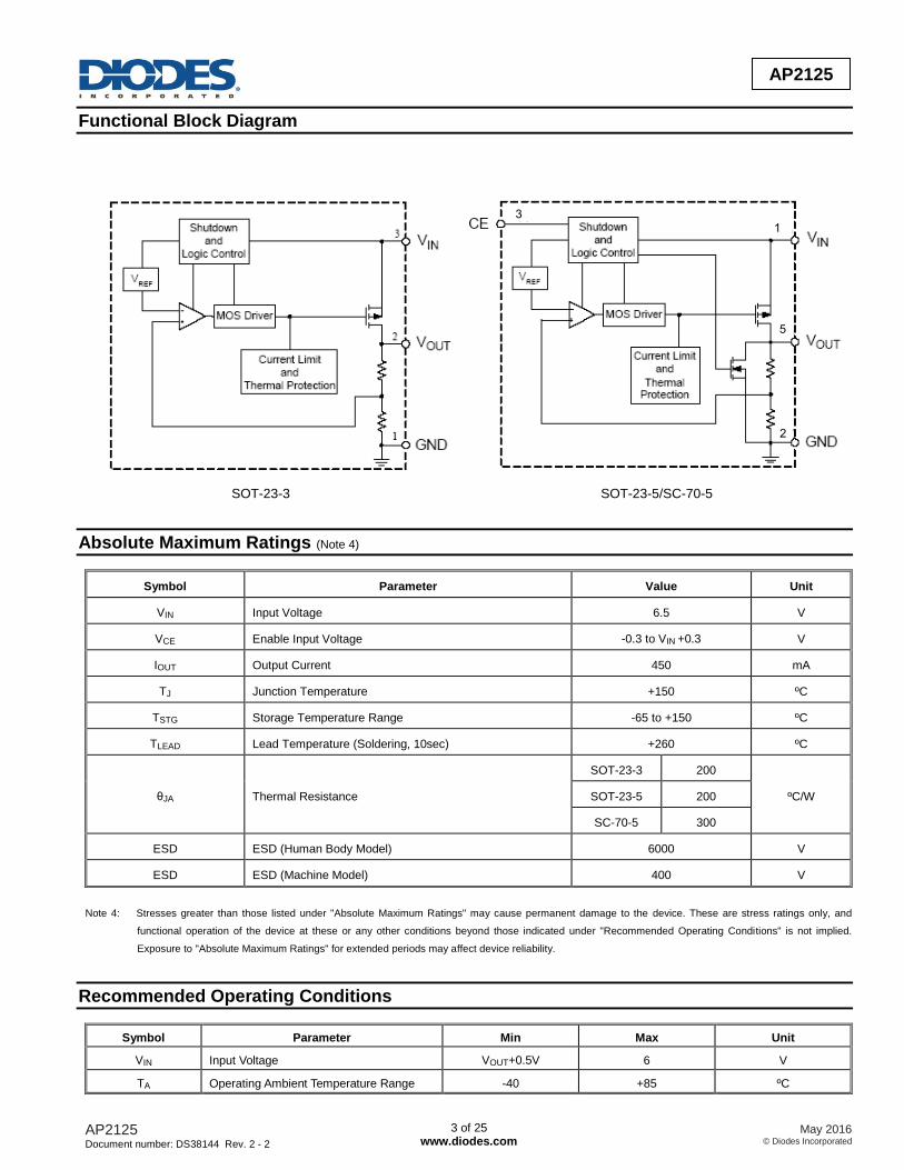
Each of these ICs is equipped with a voltage reference, an error
amplifier, a resistor network for setting output voltage, a chip enable
circuit, a current limit circuit and OTSD (over temperature shut down)
circuit to prevent the IC from over current and over temperature.
The AP2125 series have features of high ripple rejection, low dropout
voltage, low noise, high output voltage accuracy and low current
consumption which make them ideal for use in various battery-
powered apparatus.
The AP2125 have 1.8V, 2.5V, 2.8V, 3.0V, 3.3V, 4.15V and 4.2V fixed
voltage versions.
These ICs are available in tiny SC-70-5 packages as well as industry
standard SOT-23-3 and SOT-23-5 packages.
Features
Excellent Ripple Rejection: 70dB Typical (1.8V Version)
Low Dropout Voltage: 65mV (IOUT=100mA, 3.3V Version)
Low Standby Current: 0.01µA Typical
Low Quiescent Current: 60µA Typical
Extremely Low Noise: 50µVrms Typical
Maximum Output Current: 300mA (Min.)
High Output Voltage Accuracy: ±2%
Compatible with Low ESR Ceramic Capacitor
Excellent Line/Load Regulation
Totally Lead-Free & Fully RoHS Compliant (Notes 1 & 2)
Halogen and Antimony Free. “Green” Device (Note 3)
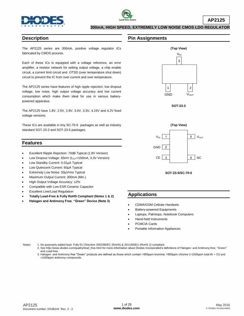
Pin Assignments
(Top View)
SOT-23-3
(Top View)
SOT-23-5/SC-70-5
Applications
CDMA/GSM Cellular Handsets
Battery-powered Equipments
Laptops, Palmtops, Notebook Computers
Hand-held Instruments
PCMCIA Cards
Portable Information Appliances
Notes: 1. No purposely added lead. Fully EU Directive 2002/95/EC (RoHS) & 2011/65/EU (RoHS 2) compliant. 2. See http://www.diodes.com/quality/lead_free.html for more information about Diodes Incorporated’s definitions of Halogen- and Antimony-free, "Green" and Lead-free. 3. Halogen- and Antimony-free "Green” products are defined as those which contain <900ppm bromine, <900ppm chlorine (<1500ppm total Br + Cl) and <1000ppm antimony compounds.
3
21
VIN
GND VOUT
VIN
GND
VOUT1
2
3 4
5
NCCE
AP2125 Document number: DS38144 Rev. 2 - 2
2 of 25 www.diodes.com
May 2016 © Diodes Incorporated
AD
VA
NC
ED
IN
FO
RM
AT
IO
N
AP2125
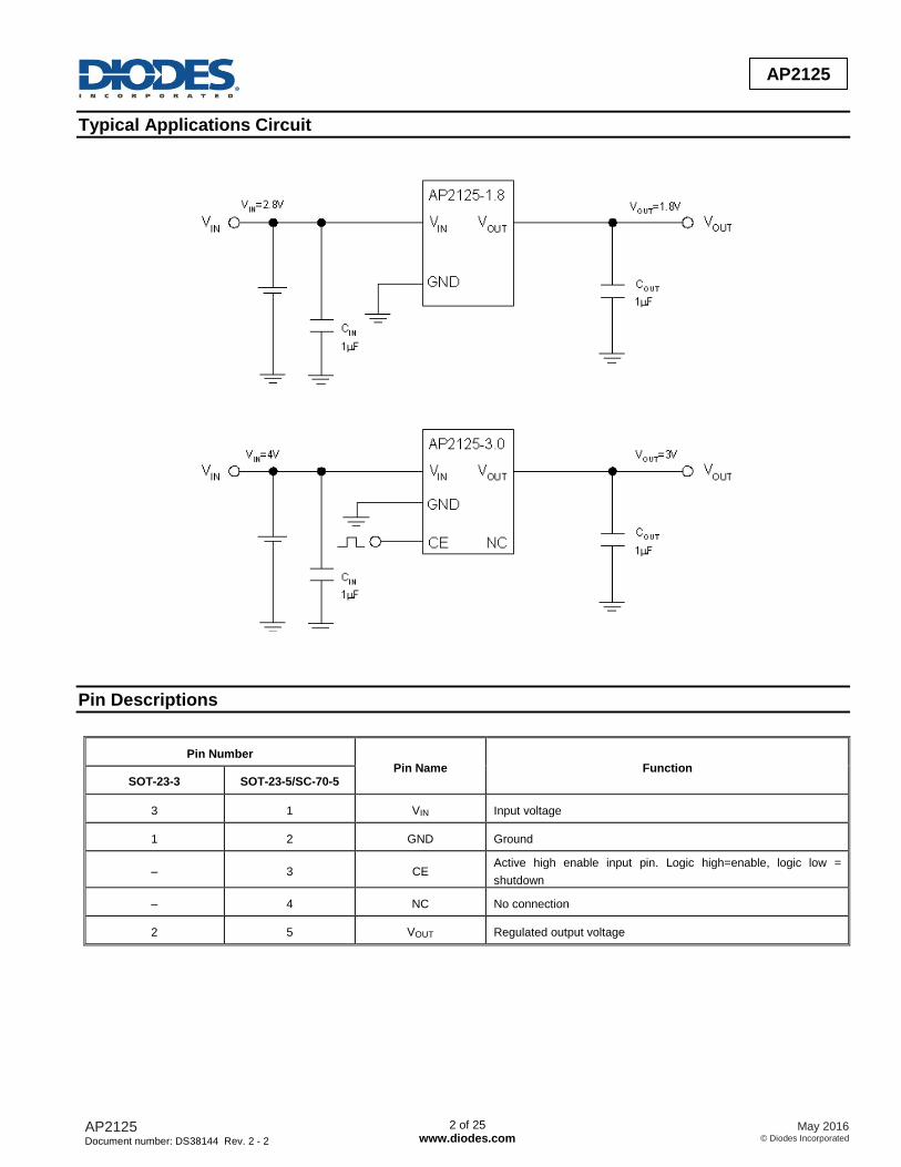
Typical Applications Circuit
Pin Descriptions
Pin Number
Pin Name Function SOT-23-3 SOT-23-5/SC-70-5
3 1 VIN Input voltage
1 2 GND Ground
– 3 CE Active high enable input pin. Logic high=enable, logic low =
shutdown
– 4 NC No connection
2 5 VOUT Regulated output voltage
AP2125 Document number: DS38144 Rev. 2 - 2
3 of 25 www.diodes.com
May 2016 © Diodes Incorporated
AD
VA
NC
ED
IN
FO
RM
AT
IO
N
AP2125
Functional Block Diagram
31
5
2
SOT-23-3 SOT-23-5/SC-70-5
Absolute Maximum Ratings (Note 4)
Symbol Parameter Value Unit
VIN Input Voltage 6.5 V
VCE Enable Input Voltage -0.3 to VIN +0.3 V
IOUT Output Current 450 mA
TJ Junction Temperature +150 ºC
TSTG Storage Temperature Range -65 to +150 ºC
TLEAD Lead Temperature (Soldering, 10sec) +260 ºC
θJA Thermal Resistance
SOT-23-3 200
ºC/W SOT-23-5 200
SC-70-5 300
ESD ESD (Human Body Model) 6000 V
ESD ESD (Machine Model) 400 V
Note 4: Stresses greater than those listed under "Absolute Maximum Ratings" may cause permanent damage to the device. These are stress ratings only, and
functional operation of the device at these or any other conditions beyond those indicated under "Recommended Operating Conditions" is not implied.
Exposure to "Absolute Maximum Ratings" for extended periods may affect device reliability.
Recommended Operating Conditions
Symbol Parameter Min Max Unit
VIN Input Voltage VOUT+0.5V 6 V
TA Operating Ambient Temperature Range -40 +85 ºC
AP2125 Document number: DS38144 Rev. 2 - 2
4 of 25 www.diodes.com
May 2016 © Diodes Incorporated
AD
VA
NC
ED
IN
FO
RM
AT
IO
N
AP2125
Electrical Characteristics
AP2125-1.8 Electrical Characteristics (@VIN = 2.8V, TA = +25oC, CIN = 1µF, COUT = 1µF, Bold typeface applies over -40
oC ≤ TJ ≤ +85
oC,
unless otherwise specified.)
Symbol Parameter Conditions Min Typ Max Unit
VOUT Output Voltage VIN = 2.8V
1mA ≤ IOUT ≤ 30mA 1.764 1.8 1.836 V
VIN Input Voltage – – – 6 V
IOUT(MAX) Maximum Output Current VIN-VOUT = 1V, VOUT = 1.76V 300 360 – mA
VRLOAD Load Regulation VIN = 2.8V
1mA ≤ IOUT ≤ 300mA – 6 15 mV
VRLINE Line Regulation 2.8V ≤ VIN ≤ 6V
IOUT = 30mA – 1 15 mV
VDROP Dropout Voltage
IOUT = 10mA – 10 12
mV IOUT = 100mA – 100 120
IOUT = 300mA – 300 360
IQ Quiescent Current VIN = 2.8V, IOUT = 0mA – 60 90 µA
ISTD Standby Current VIN = 2.8V
VCE in OFF mode – 0.01 1.0 µA
PSRR Power Supply Rejection Ratio Ripple 0.5Vp-p,
VIN = 2.8V
f = 100Hz – 70 – dB
f = 1KHz – 70 – dB
(∆VOUT/VOUT)/∆T Output Voltage
Temperature Coefficient IOUT = 30mA – ±100 – ppm/
oC
ISHORT Short Current Limit VOUT = 0V – 50 – mA
VNOISE RMS Output Noise 10Hz ≤ f ≤ 100kHz – 50 – µVrms
– CE "High" Voltage CE input voltage "High" 1.5 – – V
– CE "Low" Voltage CE input voltage "Low" – – 0.4 V
– Thermal Shutdown – – +160 – oC
– Thermal Shutdown Hysteresis – – +25 – oC
AP2125 Document number: DS38144 Rev. 2 - 2
5 of 25 www.diodes.com
May 2016 © Diodes Incorporated
AD
VA
NC
ED
IN
FO
RM
AT
IO
N
AP2125
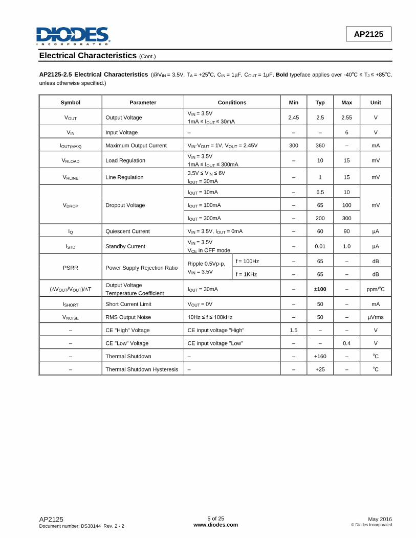
Electrical Characteristics (Cont.)
AP2125-2.5 Electrical Characteristics (@VIN = 3.5V, TA = +25oC, CIN = 1µF, COUT = 1µF, Bold typeface applies over -40
oC ≤ TJ ≤ +85
oC,
unless otherwise specified.)
Symbol Parameter Conditions Min Typ Max Unit
VOUT Output Voltage VIN = 3.5V
1mA ≤ IOUT ≤ 30mA 2.45 2.5 2.55 V
VIN Input Voltage – – – 6 V
IOUT(MAX) Maximum Output Current VIN-VOUT = 1V, VOUT = 2.45V 300 360 – mA
VRLOAD Load Regulation VIN = 3.5V
1mA ≤ IOUT ≤ 300mA – 10 15 mV
VRLINE Line Regulation 3.5V ≤ VIN ≤ 6V
IOUT = 30mA – 1 15 mV
VDROP Dropout Voltage
IOUT = 10mA – 6.5 10
mV IOUT = 100mA – 65 100
IOUT = 300mA – 200 300
IQ Quiescent Current VIN = 3.5V, IOUT = 0mA – 60 90 µA
ISTD Standby Current VIN = 3.5V
VCE in OFF mode – 0.01 1.0 µA
PSRR Power Supply Rejection Ratio Ripple 0.5Vp-p,
VIN = 3.5V
f = 100Hz – 65 – dB
f = 1KHz – 65 – dB
(∆VOUT/VOUT)/∆T Output Voltage
Temperature Coefficient IOUT = 30mA – ±100 – ppm/
oC
ISHORT Short Current Limit VOUT = 0V – 50 – mA
VNOISE RMS Output Noise 10Hz ≤ f ≤ 100kHz – 50 – µVrms
– CE "High" Voltage CE input voltage "High" 1.5 – – V
– CE "Low" Voltage CE input voltage "Low" – – 0.4 V
– Thermal Shutdown – – +160 – oC
– Thermal Shutdown Hysteresis – – +25 – oC

AP2125 Document number: DS38144 Rev. 2 - 2
6 of 25 www.diodes.com
May 2016 © Diodes Incorporated
AD
VA
NC
ED
IN
FO
RM
AT
IO
N
AP2125
Electrical Characteristics (Cont.)
AP2125-2.8 Electrical Characteristics (@VIN = 3.8V, TA = +25oC, CIN = 1µF, COUT = 1µF, Bold typeface applies over -40
oC ≤ TJ ≤ +85
oC,
unless otherwise specified.)
Symbol Parameter Conditions Min Typ Max Unit
VOUT Output Voltage VIN = 3.8V
1mA ≤ IOUT ≤ 30mA 2.744 2.8 2.856 V
VIN Input Voltage – – – 6 V
IOUT(MAX) Maximum Output Current VIN-VOUT = 1V, VOUT = 2.74V 300 360 – mA
VRLOAD Load Regulation VIN = 3.8V
1mA ≤ IOUT ≤ 300mA – 11 15 mV
VRLINE Line Regulation 3.8V ≤ VIN ≤ 6V
IOUT = 30mA – 1 15 mV
VDROP Dropout Voltage
IOUT = 10mA – 6.5 10
mV IOUT = 100mA – 65 100
IOUT = 300mA – 200 300
IQ Quiescent Current VIN = 3.8V, IOUT = 0mA – 60 90 µA
ISTD Standby Current VIN = 3.8V
VCE in OFF mode – 0.01 1.0 µA
PSRR Power Supply Rejection Ratio Ripple 0.5Vp-p,
VIN = 3.8V
f = 100Hz – 65 – dB
f = 1KHz – 65 – dB
(∆VOUT/VOUT)/∆T Output Voltage
Temperature Coefficient IOUT = 30mA – ±100 – ppm/
oC
ISHORT Short Current Limit VOUT = 0V – 50 – mA
VNOISE RMS Output Noise 10Hz ≤ f ≤ 100kHz – 50 – µVrms
– CE "High" Voltage CE input voltage "High" 1.5 – – V
– CE "Low" Voltage CE input voltage "Low" – – 0.4 V
– Thermal Shutdown – – +160 – oC
– Thermal Shutdown Hysteresis – – +25 – oC

AP2125 Document number: DS38144 Rev. 2 - 2
7 of 25 www.diodes.com
May 2016 © Diodes Incorporated
AD
VA
NC
ED
IN
FO
RM
AT
IO
N
AP2125
Electrical Characteristics (Cont.)
AP2125-3.0 Electrical Characteristics (@VIN = 4.0V, TA = +25oC, CIN = 1µF, COUT = 1µF, Bold typeface applies over -40
oC ≤ TJ ≤ +85
oC,
unless otherwise specified.)
Symbol Parameter Conditions Min Typ Max Unit
VOUT Output Voltage VIN = 4.0V
1mA ≤ IOUT ≤ 30mA 2.94 3.0 3.06 V
VIN Input Voltage – – – 6 V
IOUT(MAX) Maximum Output Current VIN-VOUT = 1V, VOUT = 2.94V 300 360 – mA
VRLOAD Load Regulation VIN = 4.0V
1mA ≤ IOUT ≤ 300mA – 12 15 mV
VRLINE Line Regulation 4.0V ≤ VIN ≤ 6V
IOUT = 30mA – 1 15 mV
VDROP Dropout Voltage
IOUT = 10mA – 6.5 10
mV IOUT = 100mA – 65 100
IOUT = 300mA – 200 300
IQ Quiescent Current VIN = 4.0V, IOUT = 0mA – 60 90 µA
ISTD Standby Current VIN = 4.0V
VCE in OFF mode – 0.01 1.0 µA
PSRR Power Supply Rejection Ratio Ripple 0.5Vp-p,
VIN = 4.0V
f = 100Hz – 65 – dB
f = 1KHz – 65 – dB
(∆VOUT/VOUT)/∆T Output Voltage
Temperature Coefficient IOUT = 30mA – ±100 – ppm/
oC
ISHORT Short Current Limit VOUT = 0V – 50 – mA
VNOISE RMS Output Noise 10Hz ≤ f ≤ 100kHz – 50 – µVrms
– CE "High" Voltage CE input voltage "High" 1.5 – – V
– CE "Low" Voltage CE input voltage "Low" – – 0.4 V
– Thermal Shutdown – – +160 – oC
– Thermal Shutdown Hysteresis – – +25 – oC

AP2125 Document number: DS38144 Rev. 2 - 2
8 of 25 www.diodes.com
May 2016 © Diodes Incorporated
AD
VA
NC
ED
IN
FO
RM
AT
IO
N
AP2125
Electrical Characteristics (Cont.)
AP2125-3.3 Electrical Characteristics (@VIN = 4.3V, TA = +25oC, CIN = 1µF, COUT = 1µF, Bold typeface applies over -40
oC ≤ TJ ≤ +85
oC,
unless otherwise specified.)
Symbol Parameter Conditions Min Typ Max Unit
VOUT Output Voltage VIN = 4.3V
1mA ≤ IOUT ≤ 30mA 3.234 3.3 3.366 V
VIN Input Voltage – – – 6 V
IOUT(MAX) Maximum Output Current VIN-VOUT = 1V, VOUT = 3.23V 300 360 – mA
VRLOAD Load Regulation VIN = 4.3V
1mA ≤ IOUT ≤ 300mA – 13 15 mV
VRLINE Line Regulation 4.3V ≤ VIN ≤ 6V
IOUT = 30mA – 1 15 mV
VDROP Dropout Voltage
IOUT = 10mA – 6.5 10
mV IOUT = 100mA – 65 100
IOUT = 300mA – 200 300
IQ Quiescent Current VIN = 4.3V, IOUT = 0mA – 60 90 µA
ISTD Standby Current VIN = 4.3V
VCE in OFF mode – 0.01 1.0 µA
PSRR Power Supply Rejection Ratio Ripple 0.5Vp-p,
VIN = 4.3V
f = 100Hz – 65 – dB
f = 1KHz – 65 – dB
(∆VOUT/VOUT)/∆T Output Voltage
Temperature Coefficient IOUT = 30mA – ±100 – ppm/
oC
ISHORT Short Current Limit VOUT = 0V – 50 – mA
VNOISE RMS Output Noise 10Hz ≤ f ≤ 100kHz – 50 – µVrms
– CE "High" Voltage CE input voltage "High" 1.5 – – V
– CE "Low" Voltage CE input voltage "Low" – – 0.4 V
– Thermal Shutdown – – +160 – oC
– Thermal Shutdown Hysteresis – – +25 – oC
AP2125 Document number: DS38144 Rev. 2 - 2
9 of 25 www.diodes.com
May 2016 © Diodes Incorporated
AD
VA
NC
ED
IN
FO
RM
AT
IO
N
AP2125
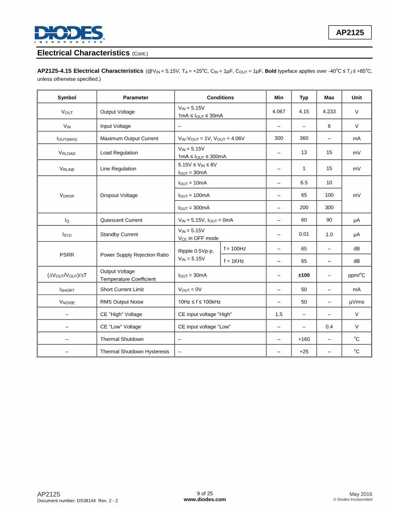
Electrical Characteristics (Cont.)
AP2125-4.15 Electrical Characteristics (@VIN = 5.15V, TA = +25oC, CIN = 1µF, COUT = 1µF, Bold typeface applies over -40
oC ≤ TJ ≤ +85
oC,
unless otherwise specified.)
Symbol Parameter Conditions Min Typ Max Unit
VOUT Output Voltage VIN = 5.15V
1mA ≤ IOUT ≤ 30mA 4.067 4.15 4.233 V
VIN Input Voltage – – – 6 V
IOUT(MAX) Maximum Output Current VIN-VOUT = 1V, VOUT = 4.06V 300 360 – mA
VRLOAD Load Regulation VIN = 5.15V
1mA ≤ IOUT ≤ 300mA – 13 15 mV
VRLINE Line Regulation 5.15V ≤ VIN ≤ 6V
IOUT = 30mA – 1 15 mV
VDROP Dropout Voltage
IOUT = 10mA – 6.5 10
mV IOUT = 100mA – 65 100
IOUT = 300mA – 200 300
IQ Quiescent Current VIN = 5.15V, IOUT = 0mA – 60 90 µA
ISTD Standby Current VIN = 5.15V
VCE in OFF mode – 0.01 1.0 µA
PSRR Power Supply Rejection Ratio Ripple 0.5Vp-p,
VIN = 5.15V
f = 100Hz – 65 – dB
f = 1KHz – 65 – dB
(∆VOUT/VOUT)/∆T Output Voltage
Temperature Coefficient IOUT = 30mA – ±100 – ppm/
oC
ISHORT Short Current Limit VOUT = 0V – 50 – mA
VNOISE RMS Output Noise 10Hz ≤ f ≤ 100kHz – 50 – µVrms
– CE "High" Voltage CE input voltage "High" 1.5 – – V
– CE "Low" Voltage CE input voltage "Low" – – 0.4 V
– Thermal Shutdown – – +160 – oC
– Thermal Shutdown Hysteresis – – +25 – oC
AP2125 Document number: DS38144 Rev. 2 - 2
10 of 25 www.diodes.com
May 2016 © Diodes Incorporated
AD
VA
NC
ED
IN
FO
RM
AT
IO
N
AP2125
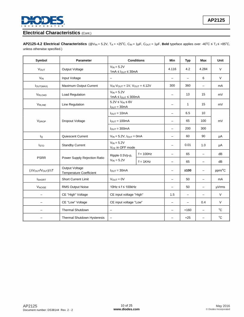
Electrical Characteristics (Cont.)
AP2125-4.2 Electrical Characteristics (@VIN = 5.2V, TA = +25oC, CIN = 1µF, COUT = 1µF, Bold typeface applies over -40
oC ≤ TJ ≤ +85
oC,
unless otherwise specified.)
Symbol Parameter Conditions Min Typ Max Unit
VOUT Output Voltage VIN = 5.2V
1mA ≤ IOUT ≤ 30mA 4.116 4.2 4.284 V
VIN Input Voltage – – – 6 V
IOUT(MAX) Maximum Output Current VIN-VOUT = 1V, VOUT = 4.12V 300 360 – mA
VRLOAD Load Regulation VIN = 5.2V
1mA ≤ IOUT ≤ 300mA – 13 15 mV
VRLINE Line Regulation 5.2V ≤ VIN ≤ 6V
IOUT = 30mA – 1 15 mV
VDROP Dropout Voltage
IOUT = 10mA – 6.5 10
mV IOUT = 100mA – 65 100
IOUT = 300mA – 200 300
IQ Quiescent Current VIN = 5.2V, IOUT = 0mA – 60 90 µA
ISTD Standby Current VIN = 5.2V
VCE in OFF mode – 0.01 1.0 µA
PSRR Power Supply Rejection Ratio Ripple 0.5Vp-p,
VIN = 5.2V
f = 100Hz – 65 – dB
f = 1KHz – 65 – dB
(∆VOUT/VOUT)/∆T Output Voltage
Temperature Coefficient IOUT = 30mA – ±100 – ppm/
oC
ISHORT Short Current Limit VOUT = 0V – 50 – mA
VNOISE RMS Output Noise 10Hz ≤ f ≤ 100kHz – 50 – µVrms
– CE "High" Voltage CE input voltage "High" 1.5 – – V
– CE "Low" Voltage CE input voltage "Low" – – 0.4 V
– Thermal Shutdown – – +160 – oC
– Thermal Shutdown Hysteresis – – +25 – oC
AP2125 Document number: DS38144 Rev. 2 - 2
11 of 25 www.diodes.com
May 2016 © Diodes Incorporated
AD
VA
NC
ED
IN
FO
RM
AT
IO
N
AP2125
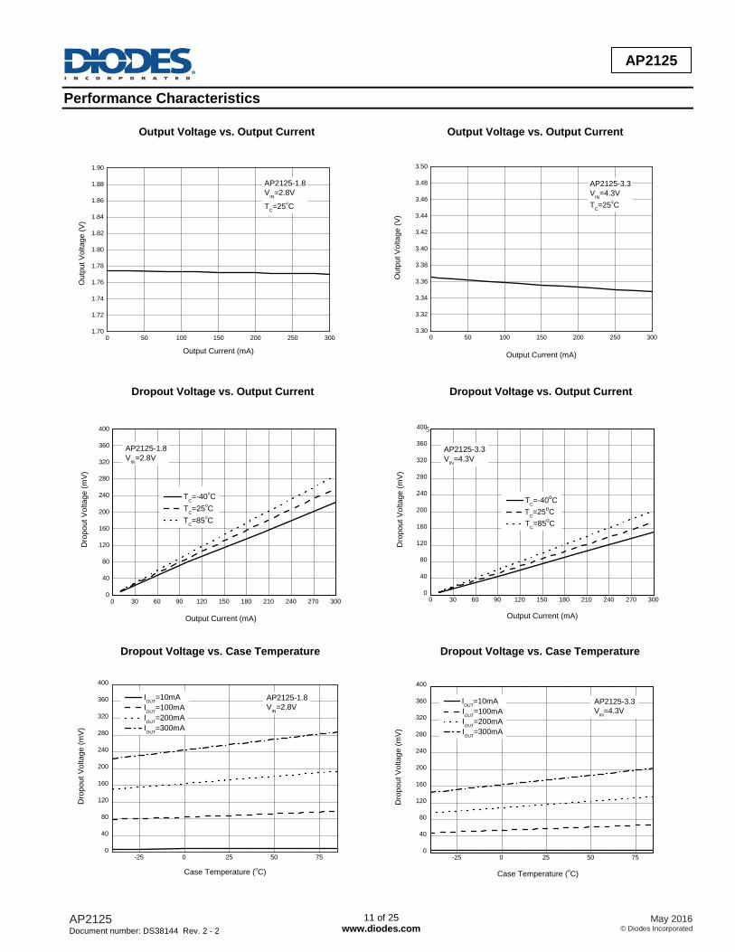
Performance Characteristics
Output Voltage vs. Output Current Output Voltage vs. Output Current
Dropout Voltage vs. Output Current Dropout Voltage vs. Output Current
Dropout Voltage vs. Case Temperature Dropout Voltage vs. Case Temperature
0 50 100 150 200 250 3003.30
3.32
3.34
3.36
3.38
3.40
3.42
3.44
3.46
3.48
3.50
AP2125-3.3
VIN
=4.3V
TC=25
oC
Ou
tpu
t V
olta
ge
(V
)
Output Current (mA)
0 30 60 90 120 150 180 210 240 270 3000
40
80
120
160
200
240
280
320
360
400
AP2125-1.8
VIN
=2.8V
TC=-40
oC
TC=25
oC
TC=85
oC
Dro
po
ut V
olta
ge
(m
V)
Output Current (mA)
0 30 60 90 120 150 180 210 240 270 3000
40
80
120
160
200
240
280
320
360
400
TC=-40
oC
TC=25
oC
TC=85
oC
AP2125-3.3
VIN
=4.3V
5
Dro
po
ut V
olta
ge
(m
V)
Output Current (mA)
-25 0 25 50 750
40
80
120
160
200
240
280
320
360
400
AP2125-1.8
VIN
=2.8V
IOUT
=10mA
IOUT
=100mA
IOUT
=200mA
IOUT
=300mA
Dro
po
ut V
olta
ge
(m
V)
Case Temperature (oC)
-25 0 25 50 750
40
80
120
160
200
240
280
320
360
400
AP2125-3.3
VIN
=4.3V
IOUT
=10mA
IOUT
=100mA
IOUT
=200mA
IOUT
=300mA
Dro
po
ut V
olta
ge
(m
V)
Case Temperature (oC)
0 50 100 150 200 250 3001.70
1.72
1.74
1.76
1.78
1.80
1.82
1.84
1.86
1.88
1.90
AP2125-1.8
VIN
=2.8V
TC=25
oC
Ou
tpu
t V
olta
ge
(V
)
Output Current (mA)
AP2125 Document number: DS38144 Rev. 2 - 2
12 of 25 www.diodes.com
May 2016 © Diodes Incorporated
AD
VA
NC
ED
IN
FO
RM
AT
IO
N
AP2125
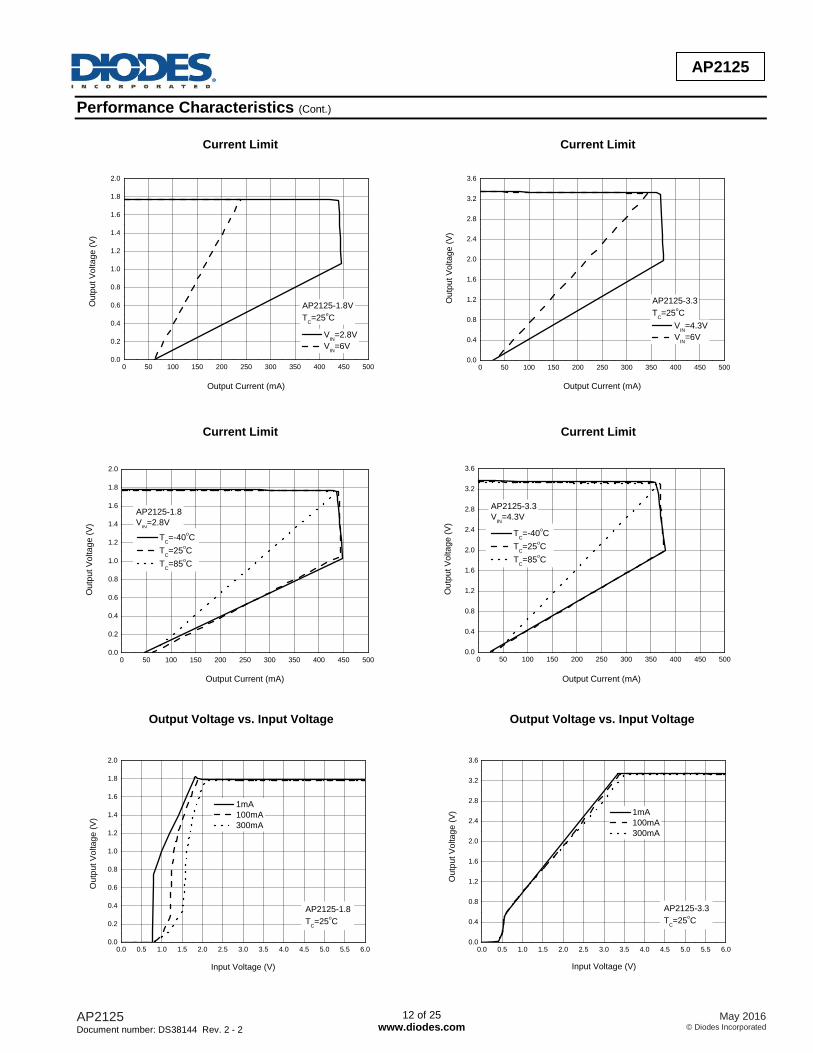
Performance Characteristics (Cont.)
Current Limit Current Limit
Current Limit Current Limit
Output Voltage vs. Input Voltage Output Voltage vs. Input Voltage
0 50 100 150 200 250 300 350 400 450 5000.0
0.4
0.8
1.2
1.6
2.0
2.4
2.8
3.2
3.6
AP2125-3.3
TC=25
oC
Ou
tpu
t V
olta
ge
(V
)
Output Current (mA)
VIN
=4.3V
VIN
=6V
0 50 100 150 200 250 300 350 400 450 5000.0
0.2
0.4
0.6
0.8
1.0
1.2
1.4
1.6
1.8
2.0
AP2125-1.8
VIN
=2.8V
Ou
tpu
t V
olta
ge
(V
)
Output Current (mA)
TC=-40
oC
TC=25
oC
TC=85
oC
0 50 100 150 200 250 300 350 400 450 5000.0
0.4
0.8
1.2
1.6
2.0
2.4
2.8
3.2
3.6
AP2125-3.3
VIN
=4.3V
Ou
tpu
t V
olta
ge
(V
)
Output Current (mA)
TC=-40
oC
TC=25
oC
TC=85
oC
0.0 0.5 1.0 1.5 2.0 2.5 3.0 3.5 4.0 4.5 5.0 5.5 6.00.0
0.2
0.4
0.6
0.8
1.0
1.2
1.4
1.6
1.8
2.0
AP2125-1.8
TC=25
oC
Ou
tpu
t V
olta
ge
(V
)
Input Voltage (V)
1mA
100mA
300mA
0.0 0.5 1.0 1.5 2.0 2.5 3.0 3.5 4.0 4.5 5.0 5.5 6.00.0
0.4
0.8
1.2
1.6
2.0
2.4
2.8
3.2
3.6
AP2125-3.3
TC=25
oC
Ou
tpu
t V
olta
ge
(V
)
Input Voltage (V)
1mA
100mA
300mA
0 50 100 150 200 250 300 350 400 450 5000.0
0.2
0.4
0.6
0.8
1.0
1.2
1.4
1.6
1.8
2.0
AP2125-1.8V
TC=25
oC
Ou
tpu
t V
olta
ge
(V
)
Output Current (mA)
VIN
=2.8V
VIN
=6V

AP2125 Document number: DS38144 Rev. 2 - 2
13 of 25 www.diodes.com
May 2016 © Diodes Incorporated
AD
VA
NC
ED
IN
FO
RM
AT
IO
N
AP2125
Performance Characteristics (Cont.)
Output Voltage vs. Input Voltage Output Voltage vs. Input Voltage
Output Voltage vs. Case Temperature Output Voltage vs. Case Temperature
Supply Current vs. Input Voltage Supply Current vs. Input Voltage
0.0 0.5 1.0 1.5 2.0 2.5 3.0 3.5 4.0 4.5 5.0 5.5 6.00.0
0.2
0.4
0.6
0.8
1.0
1.2
1.4
1.6
1.8
2.0
AP2125-1.8
TC=25
oC
No Load
Ou
tpu
t V
olta
ge
(V
)
Input Voltage (V)
TC=-40
oC
TC=25
oC
TC=85
oC
0.0 0.5 1.0 1.5 2.0 2.5 3.0 3.5 4.0 4.5 5.0 5.5 6.00.0
0.4
0.8
1.2
1.6
2.0
2.4
2.8
3.2
3.6
AP2125-3.3
TC=25
oC
No Load
Ou
tpu
t V
olta
ge
(V
)
Input Voltage (V)
TC=-40
oC
TC=25
oC
TC=85
oC
-25 0 25 50 751.70
1.72
1.74
1.76
1.78
1.80
1.82
1.84
1.86
1.88
1.90
AP2125-1.8
VIN
=2.8V
Ou
tpu
t V
olta
ge
(V
)
Case Temperature (oC)
IOUT
=10mA
IOUT
=30mA
IOUT
=100mA
IOUT
=300mA
-25 0 25 50 753.20
3.22
3.24
3.26
3.28
3.30
3.32
3.34
3.36
3.38
3.40
AP2125-3.3
VIN
=4.3V
Ou
tpu
t V
olta
ge
(V
)
Case Temperature (oC)
IOUT
=10mA
IOUT
=30mA
IOUT
=100mA
IOUT
=300mA
0 1 2 3 4 5 60
10
20
30
40
50
60
70
80
90
100
AP2125-1.8
No Load
TC=-40
oC
TC=25
oC
TC=85
oC
Su
pp
ly C
urr
en
t (
A)
Input Voltage (V)
0 1 2 3 4 5 60
10
20
30
40
50
60
70
80
90
100
TC=-40
oC
TC=25
oC
TC=85
oC
AP2125-3.3
No Load
Su
pp
ly C
urr
en
t (
A)
Input Voltage (V)

AP2125 Document number: DS38144 Rev. 2 - 2
14 of 25 www.diodes.com
May 2016 © Diodes Incorporated
AD
VA
NC
ED
IN
FO
RM
AT
IO
N
AP2125
Performance Characteristics (Cont.)
Supply Current vs. Case Temperature Supply Current vs. Case Temperature
Supply Current vs. Output Current Supply Current vs. Output Current
Supply Current vs. Output Current Supply Current vs. Output Current
-40 -20 0 20 40 60 8040
44
48
52
56
60
64
68
72
76
80
Su
pp
ly C
urr
en
t (
A)
Case Temperature (oC)
AP2125-1.8
VIN
=2.8V
No Load
-40 -20 0 20 40 60 8040
44
48
52
56
60
64
68
72
76
80
AP2125-3.3
VIN
=4.3V
No Load
Su
pp
ly C
urr
en
t (
A)
Case Temperature (oC)
0 50 100 150 200 250 300 350 400 450 5000
10
20
30
40
50
60
70
80
90
100
110
120
130
AP2125-1.8
VIN
=2.8V
Su
pp
ly C
urr
en
t (
A)
Output Current (mA)
TC=-40
oC
TC=25
oC
TC=85
oC
0 50 100 150 200 250 300 350 4000
10
20
30
40
50
60
70
80
90
100
110
120
130
140
150
AP2125-3.3
VIN
=4.3V
Su
pp
ly C
urr
en
t (
A)
Output Current (mA)
TC=-40
oC
TC=25
oC
TC=85
oC
0 40 80 120 160 200 240 280 320 360 400 440 4800
10
20
30
40
50
60
70
80
90
100
110
120
AP2125-1.8
TC=25
oC
Su
pp
ly C
urr
en
t (
A)
Output Current (mA)
VIN
=2.8V
VIN
=6V
0 40 80 120 160 200 240 280 320 360 4000
15
30
45
60
75
90
105
120
135
150
AP2125-3.3
TC=25
oC
Su
pp
ly C
urr
en
t (
A)
Output Current (mA)
VIN
=4.3V
VIN
=6V
AP2125 Document number: DS38144 Rev. 2 - 2
15 of 25 www.diodes.com
May 2016 © Diodes Incorporated
AD
VA
NC
ED
IN
FO
RM
AT
IO
N
AP2125
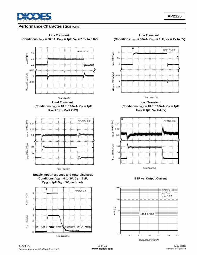
Performance Characteristics (Cont.)
Line Transient Line Transient
(Conditions: IOUT = 30mA, COUT = 1µF, VIN = 2.8V to 3.8V) (Conditions: IOUT = 30mA, COUT = 1µF, VIN = 4V to 5V)
Load Transient Load Transient
(Conditions: IOUT = 10 to 100mA, CIN = 1µF, (Conditions: IOUT = 10 to 100mA, CIN = 1µF,
COUT = 1µF, VIN = 2.8V) COUT = 1µF, VIN = 4.3V)
Enable Input Response and Auto-discharge
(Conditions: VCE = 0 to 3V, CIN = 1µF, ESR vs. Output Current
COUT = 1µF, VIN = 3V, no Load)
0 50 100 150 200 250 3000.1
1
10
100
1000
Stable Area
AP2125-1.8
CIN
= 1F
COUT
= 1F
ES
R (
)
Output Current (mA)
AP2125 Document number: DS38144 Rev. 2 - 2
16 of 25 www.diodes.com
May 2016 © Diodes Incorporated
AD
VA
NC
ED
IN
FO
RM
AT
IO
N
AP2125
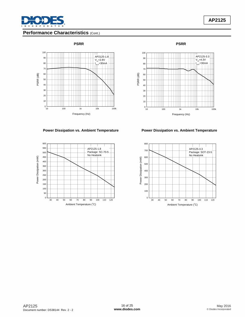
Performance Characteristics (Cont.)
PSRR PSRR
Power Dissipation vs. Ambient Temperature Power Dissipation vs. Ambient Temperature
10 100 1k 10k 100k0
10
20
30
40
50
60
70
80
90
100
PS
RR
(d
B)
Frequency (Hz)
AP2125-1.8
VIN
=2.8V
IOUT
=30mA
10 100 1k 10k 100k0
10
20
30
40
50
60
70
80
90
100
PS
RR
(d
B)
Frequency (Hz)
AP2125-3.3
VIN
=4.3V
IOUT
=30mA
30 40 50 60 70 80 90 100 110 1200
50
100
150
200
250
300
350
400
450
500
550
600
Po
we
r D
issip
atio
n (
mW
)
Ambient Temperature (oC)
AP2125-1.8
Package: SC-70-5
No Heatsink
30 40 50 60 70 80 90 100 110 1200
100
200
300
400
500
600
700
800
Po
we
r D
issip
atio
n (
mW
)
Ambient Temperature (oC)
AP2125-3.3
Package: SOT-23-5
No Heatsink
AP2125 Document number: DS38144 Rev. 2 - 2
17 of 25 www.diodes.com
May 2016 © Diodes Incorporated
AD
VA
NC
ED
IN
FO
RM
AT
IO
N
AP2125
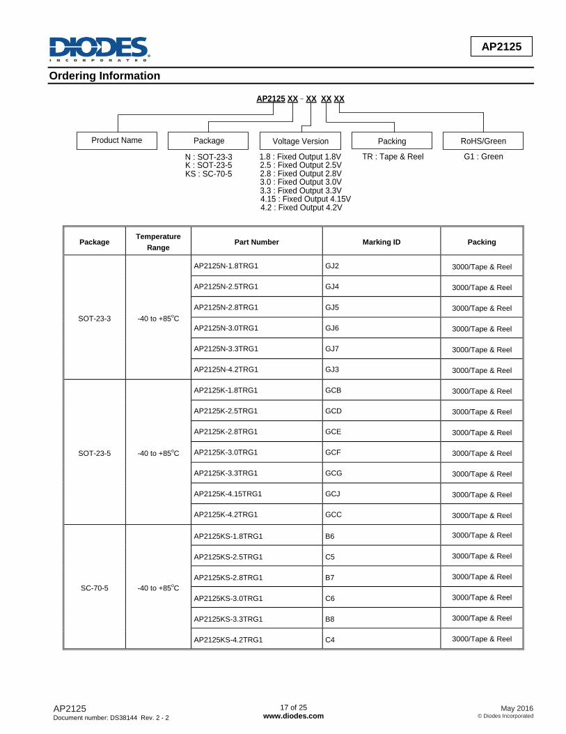
Ordering Information
AP2125 XX–XX XX XX
PackingVoltage Version
TR : Tape & ReelN : SOT-23-3K : SOT-23-5
Product Name Package
1.8 : Fixed Output 1.8V
KS : SC-70-52.5 : Fixed Output 2.5V2.8 : Fixed Output 2.8V3.0 : Fixed Output 3.0V3.3 : Fixed Output 3.3V4.15 : Fixed Output 4.15V4.2 : Fixed Output 4.2V
G1 : Green
RoHS/Green
Package Temperature
Range Part Number Marking ID Packing
SOT-23-3 -40 to +85oC
AP2125N-1.8TRG1 GJ2 3000/Tape & Reel
AP2125N-2.5TRG1 GJ4 3000/Tape & Reel
AP2125N-2.8TRG1 GJ5 3000/Tape & Reel
AP2125N-3.0TRG1 GJ6 3000/Tape & Reel
AP2125N-3.3TRG1 GJ7 3000/Tape & Reel
AP2125N-4.2TRG1 GJ3 3000/Tape & Reel
SOT-23-5 -40 to +85oC
AP2125K-1.8TRG1 GCB 3000/Tape & Reel
AP2125K-2.5TRG1 GCD 3000/Tape & Reel
AP2125K-2.8TRG1 GCE 3000/Tape & Reel
AP2125K-3.0TRG1 GCF 3000/Tape & Reel
AP2125K-3.3TRG1 GCG 3000/Tape & Reel
AP2125K-4.15TRG1 GCJ 3000/Tape & Reel
AP2125K-4.2TRG1 GCC 3000/Tape & Reel
SC-70-5 -40 to +85oC
AP2125KS-1.8TRG1 B6 3000/Tape & Reel
AP2125KS-2.5TRG1 C5 3000/Tape & Reel
AP2125KS-2.8TRG1 B7 3000/Tape & Reel
AP2125KS-3.0TRG1 C6 3000/Tape & Reel
AP2125KS-3.3TRG1 B8 3000/Tape & Reel
AP2125KS-4.2TRG1 C4 3000/Tape & Reel
AP2125 Document number: DS38144 Rev. 2 - 2
18 of 25 www.diodes.com
May 2016 © Diodes Incorporated
AD
VA
NC
ED
IN
FO
RM
AT
IO
N
AP2125
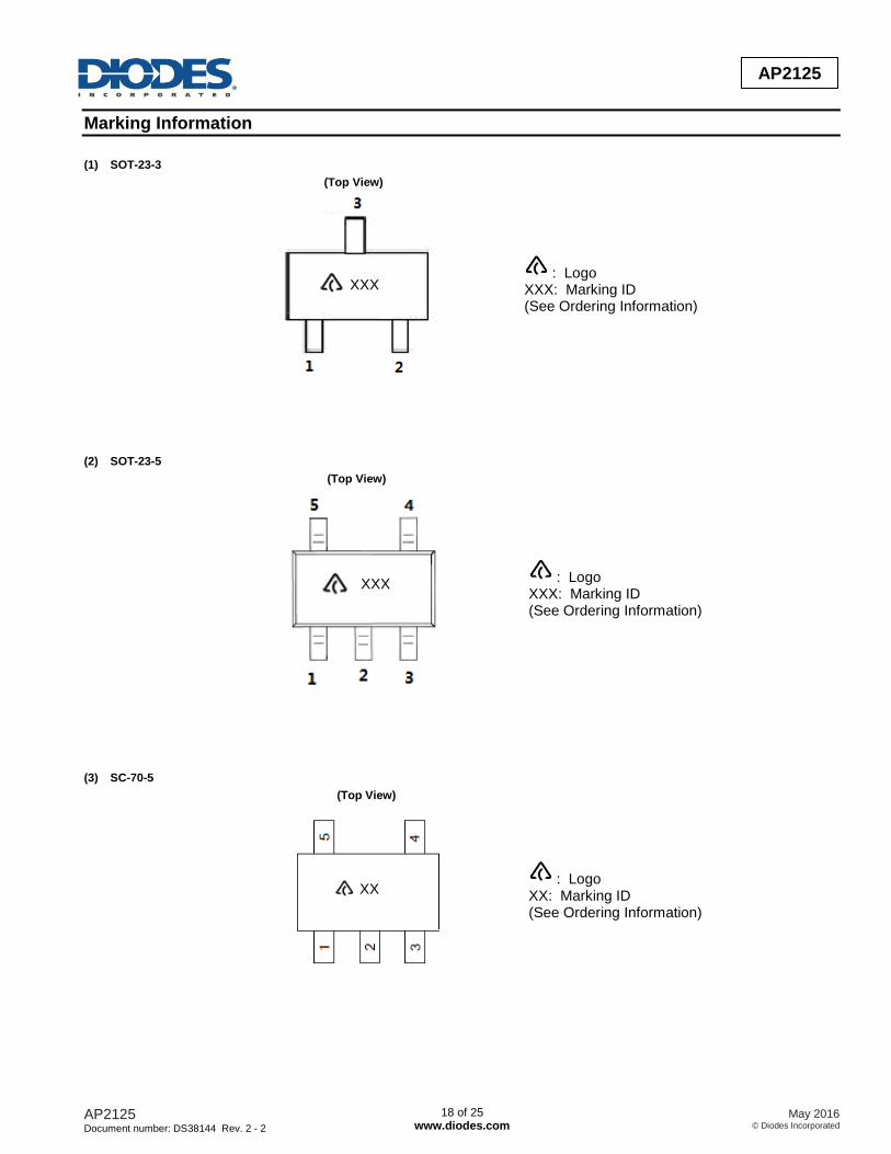
Marking Information
(1) SOT-23-3
(Top View)
(2) SOT-23-5
(Top View)
(3) SC-70-5
(Top View)
: Logo XXX: Marking ID (See Ordering Information)
: Logo XXX: Marking ID (See Ordering Information)
: Logo XX: Marking ID (See Ordering Information)
XXX
XXX
XX
AP2125 Document number: DS38144 Rev. 2 - 2
19 of 25 www.diodes.com
May 2016 © Diodes Incorporated
AD
VA
NC
ED
IN
FO
RM
AT
IO
N
AP2125
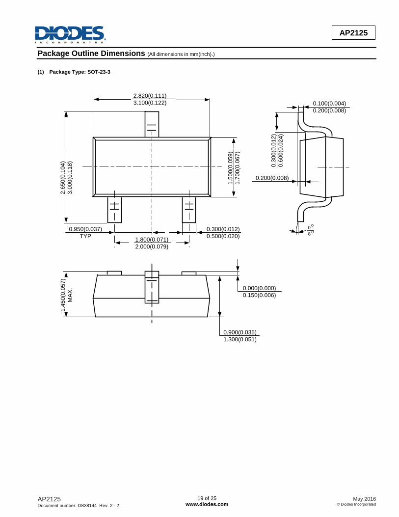
Package Outline Dimensions (All dimensions in mm(inch).)
(1) Package Type: SOT-23-3
2.820(0.111)
3.100(0.122)
2.6
50
(0.1
04
)
3.0
00
(0.1
18
)
0.950(0.037)
TYP
0.300(0.012)
0.500(0.020)1
.50
0(0
.05
9)
1.7
00(0
.06
7)
1.800(0.071)
2.000(0.079)
0.3
00
(0.0
12
)
0.6
00
(0.0
24
)
0.100(0.004)
0.200(0.008)
0.000(0.000)
0.150(0.006)
0.900(0.035)
1.300(0.051)
1.4
50
(0.0
57
)
MA
X.
0.200(0.008)
0
8
AP2125 Document number: DS38144 Rev. 2 - 2
20 of 25 www.diodes.com
May 2016 © Diodes Incorporated
AD
VA
NC
ED
IN
FO
RM
AT
IO
N
AP2125
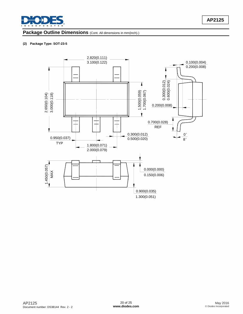
Package Outline Dimensions (Cont. All dimensions in mm(inch).)
(2) Package Type: SOT-23-5
2.820(0.111)
2.6
50(0
.10
4)
1. 5
00
(0.0
59
)
0.000(0.000)
0.300(0.012)0.950(0.037)
0.900(0.035)
0.100(0.004)
0.200(0.008)
0.3
00
(0. 0
12
)
8°
0°
3.100(0.122)
1.7
00
(0.0
67
)
3.0
00
(0.1
18
)
0.500(0.020)
0.150(0.006)
1.300(0.051)
0.200(0.008)
0.6
00
(0.0
24
)
1.800(0.071)
2.000(0.079)
0.700(0.028)
REF
TYP
1.4
50
(0.0
57
)
MA
X
AP2125 Document number: DS38144 Rev. 2 - 2
21 of 25 www.diodes.com
May 2016 © Diodes Incorporated
AD
VA
NC
ED
IN
FO
RM
AT
IO
N
AP2125
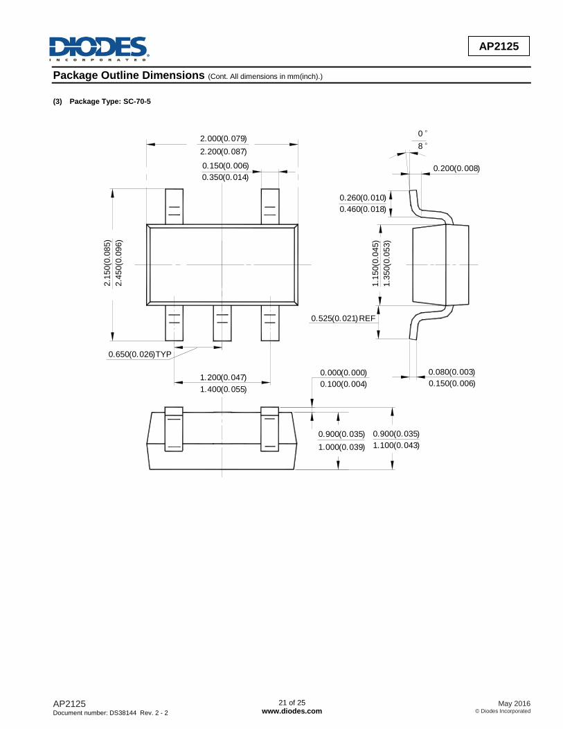
Package Outline Dimensions (Cont. All dimensions in mm(inch).)
(3) Package Type: SC-70-5
2.000(0.079)
2.200(0.087)
2.1
50(0
.08
5)
2.4
50(0
.09
6)
1.1
50(0
.04
5)
1.3
50(0
.05
3)
0.650(0.026)TYP
1.200(0.047)
1.400(0.055)
0.150(0.006)
0.350(0.014)
0.525(0.021)REF
0.080(0.003)
0.150(0.006)
0°
8°
0.200(0.008)
0.260(0.010)
0.460(0.018)
0.000(0.000)
0.100(0.004)
0.900(0.035)
1.000(0.039)
0.900(0.035)
1.100(0.043)
AP2125 Document number: DS38144 Rev. 2 - 2
22 of 25 www.diodes.com
May 2016 © Diodes Incorporated
AD
VA
NC
ED
IN
FO
RM
AT
IO
N
AP2125
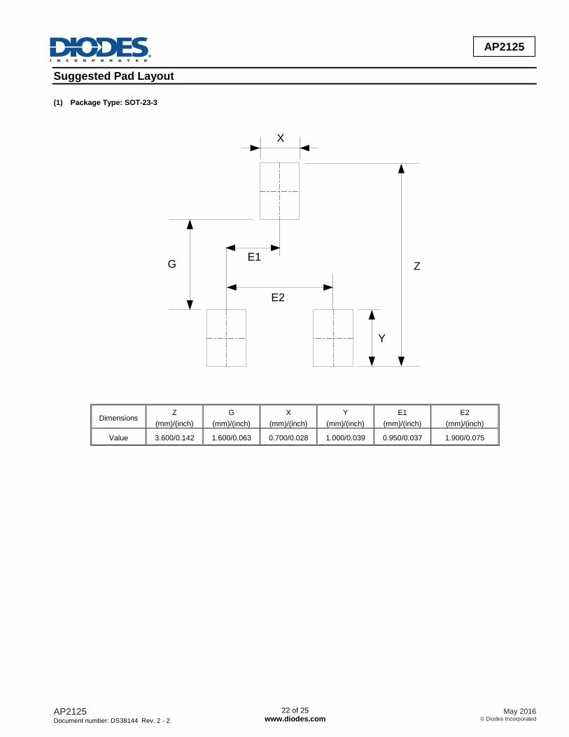
Suggested Pad Layout
(1) Package Type: SOT-23-3
Y
ZGE1
E2
X
Dimensions Z
(mm)/(inch)
G
(mm)/(inch)
X
(mm)/(inch)
Y
(mm)/(inch)
E1
(mm)/(inch)
E2
(mm)/(inch)
Value 3.600/0.142 1.600/0.063 0.700/0.028 1.000/0.039 0.950/0.037 1.900/0.075
AP2125 Document number: DS38144 Rev. 2 - 2
23 of 25 www.diodes.com
May 2016 © Diodes Incorporated
AD
VA
NC
ED
IN
FO
RM
AT
IO
N
AP2125
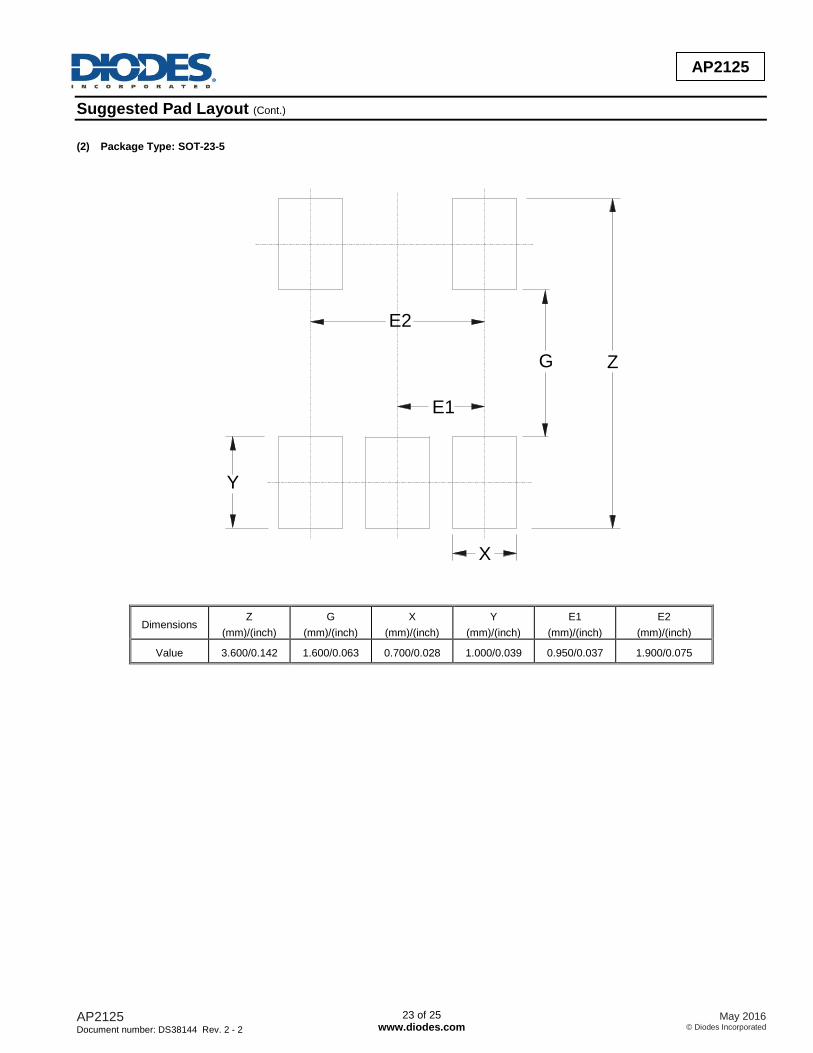
Suggested Pad Layout (Cont.)
(2) Package Type: SOT-23-5
E2
E1
Y
X
G Z
Dimensions Z
(mm)/(inch)
G
(mm)/(inch)
X
(mm)/(inch)
Y
(mm)/(inch)
E1
(mm)/(inch)
E2
(mm)/(inch)
Value 3.600/0.142 1.600/0.063 0.700/0.028 1.000/0.039 0.950/0.037 1.900/0.075
AP2125 Document number: DS38144 Rev. 2 - 2
24 of 25 www.diodes.com
May 2016 © Diodes Incorporated
AD
VA
NC
ED
IN
FO
RM
AT
IO
N
AP2125
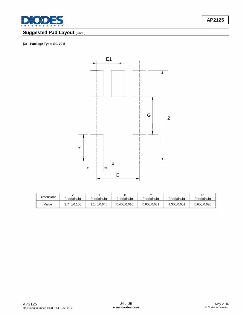
Suggested Pad Layout (Cont.)
(3) Package Type: SC-70-5
Y
X
E
G
E1
Z
Dimensions Z
(mm)/(inch) G
(mm)/(inch) X
(mm)/(inch) Y
(mm)/(inch) E
(mm)/(inch) E1
(mm)/(inch)
Value 2.740/0.108 1.140/0.045 0.400/0.016 0.800/0.031 1.300/0.051 0.650/0.026
AP2125 Document number: DS38144 Rev. 2 - 2
25 of 25 www.diodes.com
May 2016 © Diodes Incorporated
AD
VA
NC
ED
IN
FO
RM
AT
IO
N
AP2125
IMPORTANT NOTICE DIODES INCORPORATED MAKES NO WARRANTY OF ANY KIND, EXPRESS OR IMPLIED, WITH REGARDS TO THIS DOCUMENT, INCLUDING, BUT NOT LIMITED TO, THE IMPLIED WARRANTIES OF MERCHANTABILITY AND FITNESS FOR A PARTICULAR PURPOSE (AND THEIR EQUIVALENTS UNDER THE LAWS OF ANY JURISDICTION). Diodes Incorporated and its subsidiaries reserve the right to make modifications, enhancements, improvements, corrections or other changes without further notice to this document and any product described herein. Diodes Incorporated does not assume any liability arising out of the application or use of this document or any product described herein; neither does Diodes Incorporated convey any license under its patent or trademark rights, nor the rights of others. Any Customer or user of this document or products described herein in such applications shall assume all risks of such use and will agree to hold Diodes Incorporated and all the companies whose products are represented on Diodes Incorporated website, harmless against all damages. Diodes Incorporated does not warrant or accept any liability whatsoever in respect of any products purchased through unauthorized sales channel. Should Customers purchase or use Diodes Incorporated products for any unintended or unauthorized application, Customers shall indemnify and hold Diodes Incorporated and its representatives harmless against all claims, damages, expenses, and attorney fees arising out of, directly or indirectly, any claim of personal injury or death associated with such unintended or unauthorized application. Products described herein may be covered by one or more United States, international or foreign patents pending. Product names and markings noted herein may also be covered by one or more United States, international or foreign trademarks. This document is written in English but may be translated into multiple languages for reference. Only the English version of this document is the final and determinative format released by Diodes Incorporated.
LIFE SUPPORT Diodes Incorporated products are specifically not authorized for use as critical components in life support devices or systems without the express written approval of the Chief Executive Officer of Diodes Incorporated. As used herein: A. Life support devices or systems are devices or systems which: 1. are intended to implant into the body, or
2. support or sustain life and whose failure to perform when properly used in accordance with instructions for use provided in the labeling can be reasonably expected to result in significant injury to the user.
B. A critical component is any component in a life support device or system whose failure to perform can be reasonably expected to cause the failure of the life support device or to affect its safety or effectiveness. Customers represent that they have all necessary expertise in the safety and regulatory ramifications of their life support devices or systems, and acknowledge and agree that they are solely responsible for all legal, regulatory and safety-related requirements concerning their products and any use of Diodes Incorporated products in such safety-critical, life support devices or systems, notwithstanding any devices- or systems-related information or support that may be provided by Diodes Incorporated. Further, Customers must fully indemnify Diodes Incorporated and its representatives against any damages arising out of the use of Diodes Incorporated products in such safety-critical, life support devices or systems. Copyright © 2016, Diodes Incorporated www.diodes.com