tps92610-q1 datasheet - texas instruments · en out ssh tps92610 ± q1 supply 4.5 ± 40v r (sns)...
TRANSCRIPT
EN
OUT
SSH
TPS92610 ± Q1
SUPPLY
4.5 ± 40V
R(SNS)
SSLGNDGND
EN
DIAGENDIAGEN
PWMPWM
IN
FAULT FAULT
Copyright © 2017, Texas Instruments Incorporated
R2
R1
Product
Folder
Order
Now
Technical
Documents
Tools &
Software
Support &Community
ReferenceDesign
An IMPORTANT NOTICE at the end of this data sheet addresses availability, warranty, changes, use in safety-critical applications,intellectual property matters and other important disclaimers. PRODUCTION DATA.
TPS92610-Q1SLDS233A –OCTOBER 2017–REVISED DECEMBER 2017
TPS92610-Q1 Automotive Single-Channel Linear LED Driver
1
1 Features1• Qualified for Automotive Applications• AEC-Q100 Qualified With the Following Results:
– Temperature Grade 1: –40°C to 125°CAmbient Operating Temperature Range
– Device HBM ESD Classification Level H2– Device CDM ESD Classification Level C3B
• Single-Channel Constant-Current LED Driver WithPWM Dimming
• Wide Input-Voltage Range: 4.5 V–40 V• Constant Output Current, Adjustable by Sense
Resistor• Precision Current Regulation, Tolerance ±4.6%
Across Junction Temperature –40°C to 150°C• Maximum Current: 450 mA• Heat Sharing With External Resistor• Low Dropout Voltage (Sense–Resistor Voltage
Drop Included)– Maximum Dropout: 150 mV at 10 mA– Maximum Dropout: 400 mV at 70 mA– Maximum Dropout: 700 mV at 150 mA– Maximum Dropout: 1.3 V at 300 mA
• Diagnostics and Protection– Single-LED Short-Circuit Detection With Auto-
Recovery– LED Open-Circuit and Short-Circuit Detection
With Auto-Recovery– Diagnostic-Enable With Adjustable Threshold
for Low-Dropout Operation– Fault Bus up to 15 Devices, Configurable As
Either One-Fails–All-Fail or Only-Failed-Channel-Off
– Low Quiescent Current and Fault-ModeCurrent (<250 µA per Device)
• Operating Junction Temperature Range: –40°C to150°C
2 Applications• Automotive Convenience Lighting: Dome Light,
Door Handles, Reading Lamp, and MiscellaneousLamps
• Automotive Rear Lamp, Center High-MountedStop Lamp, Side Markers, Blind-Spot DetectionIndicator, Charging Inlet Indicator
• General-Purpose LED Driver Application
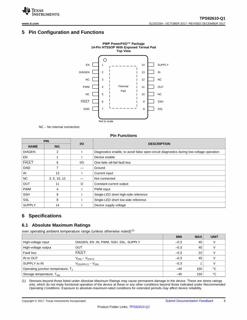
3 DescriptionWith LEDs being widely used in automotiveapplications, simple LED drivers are more and morepopular. Compared to discrete solutions, a low-costmonolithic solution lowers system level componentcounts and significantly improves current accuracyand reliability.
The TPS92610-Q1 device is a simple single-channelhigh-side LED driver operating from an automotivecar battery. It is a simple and elegant solution todeliver constant current for a single LED string withfull LED diagnostics. Its one-fails–all-fail feature isable to work together with other LED drivers, such asthe TPS9261x-Q1, TPS9263x-Q1, and TPS9283x-Q1devices, to address different requirements.
Device Information(1)
PART NUMBER PACKAGE BODY SIZE (NOM)TPS92610-Q1 HTSSOP (14) 5 mm × 4.4 mm
(1) For all available packages, see the orderable addendum atthe end of the data sheet.
Typical Application Diagram

2
TPS92610-Q1SLDS233A –OCTOBER 2017–REVISED DECEMBER 2017 www.ti.com
Product Folder Links: TPS92610-Q1
Submit Documentation Feedback Copyright © 2017, Texas Instruments Incorporated
Table of Contents1 Features .................................................................. 12 Applications ........................................................... 13 Description ............................................................. 14 Revision History..................................................... 25 Pin Configuration and Functions ......................... 36 Specifications......................................................... 3
6.1 Absolute Maximum Ratings ...................................... 36.2 ESD Ratings.............................................................. 46.3 Recommended Operating Conditions....................... 46.4 Thermal Information .................................................. 46.5 Electrical Characteristics........................................... 46.6 Timing Requirements ................................................ 66.7 Typical Characteristics .............................................. 7
7 Detailed Description ............................................ 107.1 Overview ................................................................. 107.2 Functional Block Diagram ....................................... 10
7.3 Feature Description................................................. 107.4 Device Functional Modes........................................ 14
8 Application and Implementation ........................ 168.1 Application Information............................................ 168.2 Typical Application .................................................. 16
9 Layout ................................................................... 209.1 Layout Guidelines ................................................... 209.2 Layout Example ...................................................... 20
10 Device and Documentation Support ................. 2110.1 Documentation Support ....................................... 2110.2 Receiving Notification of Documentation Updates 2110.3 Community Resources.......................................... 2110.4 Trademarks ........................................................... 2110.5 Electrostatic Discharge Caution............................ 2110.6 Glossary ................................................................ 21
11 Mechanical, Packaging, and OrderableInformation ........................................................... 22
4 Revision History
Changes from Original (November 2017) to Revision A Page
• Changed data sheet from ADVANCE INFORMATION to PRODUCTION DATA .................................................................. 1
1EN 14 SUPPLY
2DIAGEN 13 IN
3NC 12 NC
4PWM 11 OUT
5NC 10 NC
6FAULT 9 SSH
7GND 8 SSL
Not to scale
Thermal
Pad
3
TPS92610-Q1www.ti.com SLDS233A –OCTOBER 2017–REVISED DECEMBER 2017
Product Folder Links: TPS92610-Q1
Submit Documentation FeedbackCopyright © 2017, Texas Instruments Incorporated
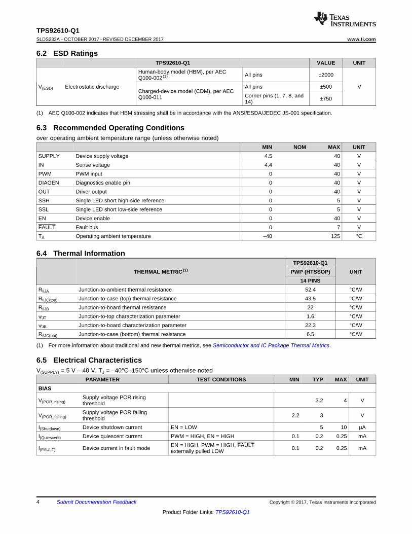
5 Pin Configuration and Functions
PWP PowerPAD™ Package14-Pin HTSSOP With Exposed Termal Pad
Top View
NC – No internal connection
Pin FunctionsPIN
I/O DESCRIPTIONNAME NO.
DIAGEN 2 I Diagnostics enable, to avoid false open-circuit diagnostics during low-voltage operationEN 1 I Device enableFAULT 6 I/O One-fails–all-fail fault busGND 7 — GroundIN 13 I Current inputNC 3, 5, 10, 12 — Not connectedOUT 11 O Constant-current outputPWM 4 I PWM inputSSH 9 I Single-LED short high-side referenceSSL 8 I Single-LED short low-side referenceSUPPLY 14 I Device supply voltage
(1) Stresses beyond those listed under Absolute Maximum Ratings may cause permanent damage to the device. These are stress ratingsonly, which do not imply functional operation of the device at these or any other conditions beyond those indicated under RecommendedOperating Conditions. Exposure to absolute-maximum-rated conditions for extended periods may affect device reliability.
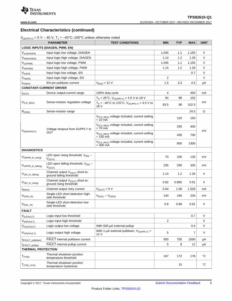
6 Specifications
6.1 Absolute Maximum Ratingsover operating ambient temperature range (unless otherwise noted) (1)
MIN MAX UNITHigh-voltage input DIAGEN, EN ,IN, PWM, SSH, SSL, SUPPLY –0.3 45 VHigh-voltage output OUT –0.3 45 VFault bus FAULT –0.3 22 VIN to OUT V(IN) – V(OUT) –0.3 45 VSUPPLY to IN V(SUPPLY) – V(IN) –0.3 1 VOperating junction temperature, TJ –40 150 °CStorage temperature, Tstg –40 150 °C
4
TPS92610-Q1SLDS233A –OCTOBER 2017–REVISED DECEMBER 2017 www.ti.com
Product Folder Links: TPS92610-Q1
Submit Documentation Feedback Copyright © 2017, Texas Instruments Incorporated
(1) AEC Q100-002 indicates that HBM stressing shall be in accordance with the ANSI/ESDA/JEDEC JS-001 specification.
6.2 ESD RatingsTPS92610-Q1 VALUE UNIT
V(ESD) Electrostatic discharge
Human-body model (HBM), per AECQ100-002 (1) All pins ±2000
VCharged-device model (CDM), per AECQ100-011
All pins ±500Corner pins (1, 7, 8, and14) ±750
6.3 Recommended Operating Conditionsover operating ambient temperature range (unless otherwise noted)
MIN NOM MAX UNITSUPPLY Device supply voltage 4.5 40 VIN Sense voltage 4.4 40 VPWM PWM input 0 40 VDIAGEN Diagnostics enable pin 0 40 VOUT Driver output 0 40 VSSH Single LED short high-side reference 0 5 VSSL Single LED short low-side reference 0 5 VEN Device enable 0 40 VFAULT Fault bus 0 7 VTA Operating ambient temperature –40 125 °C
(1) For more information about traditional and new thermal metrics, see Semiconductor and IC Package Thermal Metrics.
6.4 Thermal Information
THERMAL METRIC (1)TPS92610-Q1
UNITPWP (HTSSOP)14 PINS
RθJA Junction-to-ambient thermal resistance 52.4 °C/WRθJC(top) Junction-to-case (top) thermal resistance 43.5 °C/WRθJB Junction-to-board thermal resistance 22 °C/WψJT Junction-to-top characterization parameter 1.6 °C/WψJB Junction-to-board characterization parameter 22.3 °C/WRθJC(bot) Junction-to-case (bottom) thermal resistance 6.5 °C/W
6.5 Electrical CharacteristicsV(SUPPLY) = 5 V – 40 V, TJ = –40°C–150°C unless otherwise noted
PARAMETER TEST CONDITIONS MIN TYP MAX UNITBIAS
V(POR_rising)Supply voltage POR risingthreshold 3.2 4 V
V(POR_falling)Supply voltage POR fallingthreshold 2.2 3 V
I(Shutdown) Device shutdown current EN = LOW 5 10 µAI(Quiescent) Device quiescent current PWM = HIGH, EN = HIGH 0.1 0.2 0.25 mA
I(FAULT) Device current in fault mode EN = HIGH, PWM = HIGH, FAULTexternally pulled LOW 0.1 0.2 0.25 mA
5
TPS92610-Q1www.ti.com SLDS233A –OCTOBER 2017–REVISED DECEMBER 2017
Product Folder Links: TPS92610-Q1
Submit Documentation FeedbackCopyright © 2017, Texas Instruments Incorporated
Electrical Characteristics (continued)V(SUPPLY) = 5 V – 40 V, TJ = –40°C–150°C unless otherwise noted
PARAMETER TEST CONDITIONS MIN TYP MAX UNITLOGIC INPUTS (DIAGEN, PWM, EN)VIL(DIAGEN) Input logic-low voltage, DIAGEN 1.045 1.1 1.155 VVIH(DIAGEN) Input logic-high voltage, DIAGEN 1.14 1.2 1.26 VVIL(PWM) Input logic-low voltage, PWM 1.045 1.1 1.155 VVIH(PWM) Input logic-high voltage, PWM 1.14 1.2 1.26 VVIL(EN) Input logic-low voltage, EN 0.7 VVIH(EN) Input logic-high voltage, EN 2 VIPD(EN) EN pin pulldown current V(EN) = 12 V 1.5 3.3 4.5 µACONSTANT-CURRENT DRIVERI(OUT) Device output-current range 100% duty-cycle 4 450 mA
V(CS_REG) Sense-resistor regulation voltageTA = 25°C, V(SUPPLY) = 4.5 V to 18 V 94 98 102
mVTA = –40°C to 125°C, V(SUPPLY) = 4.5 V to18 V 93.5 98 102.5
R(SNS) Sense-resistor range 24.5 Ω
V(DROPOUT)Voltage dropout from SUPPLY toOUT
V(CS_REG) voltage included, current setting= 10 mA 120 150
mV
V(CS_REG) voltage included, current setting= 70 mA 250 400
V(CS_REG) voltage included, current setting= 150 mA 430 700
V(CS_REG) voltage included, current setting= 300 mA 800 1300
DIAGNOSTICS
V(OPEN_th_rising)LED open rising threshold, V(IN) –V(OUT)
70 100 135 mV
V(OPEN_th_falling)LED open falling threshold, V(IN) –V(OUT)
235 290 335 mV
V(SG_th_falling)Channel output V(OUT) short-to-ground falling threshold 1.14 1.2 1.26 V
V(SG_th_rising)Channel output V(OUT) short-to-ground rising threshold 0.82 0.865 0.91 V
I(Retry) Channel output retry current V(OUT) = 0 V 0.64 1.08 1.528 mA
V(SSH_th)Single-LED short-detection high-side threshold V(SSL) – V(SSH) 140 190 235 mV
V(SSL_th)Single-LED short-detection low-side threshold 0.8 0.86 0.91 V
FAULTVIL(FAULT) Logic-input low threshold 0.7 VVIH(FAULT) Logic-input high threshold 2 VVOL(FAULT) Logic-output low voltage With 500-µA external pullup 0.4 V
VOH(FAULT) Logic-output high voltage With 1-µA external pulldown, V(SUPPLY) =12 V 5 7 V
I(FAULT_pulldown) FAULT internal pulldown current 500 750 1000 µAI(FAULT_pullup) FAULT internal pullup current 5 8 12 µATHERMAL PROTECTION
T(TSD)Thermal shutdown junctiontemperature threshold 167 172 178 °C
T(TSD_HYS)Thermal shutdown junctiontemperature hysteresis 15 °C

PWM
Channel Current
IOUT10%
90%90%
10%
t1 t2 t3 t4 t5 t6
Input duty-cycle
Output duty-cycle
Copyright © 2017, Texas Instruments Incorporated
6
TPS92610-Q1SLDS233A –OCTOBER 2017–REVISED DECEMBER 2017 www.ti.com
Product Folder Links: TPS92610-Q1
Submit Documentation Feedback Copyright © 2017, Texas Instruments Incorporated
6.6 Timing RequirementsMIN NOM MAX UNIT
t(PWM_delay_rising)PWM rising edge delay, 50% PWM voltage to 10% of output current, t2 – t1as shown in Figure 1 10 17 25 µs
t(PWM_delay_falling)PWM falling edge delay, 50% PWM voltage to 90% of output current, t5 – t4as shown in Figure 1 15 21 30 µs
t(TSD_deg) Thermal overtemperature deglitch time 60 µs
t(DEVICE_STARTUP)EN rising edge to 10% output current at 150-mA set current and 12-V supplyvoltage 100 150 µs
t(OPEN_deg) LED open-circuit fault-deglitch time 80 125 175 µst(SG_deg) Channel-output short-to-ground detection deglitch time 80 125 175 µst(SS_deg) Single-LED short-detection deglitch time 80 125 175 µst(Recover_deg) Recovery deglitch time 16 µs
Figure 1. Output Timing Diagram
Supply Voltage (V)
Cur
rent
(P
A)
4 10 16 22 28 34 402
10
100
250
D004
�40qC, I(Shutdown)25qC, I(Shutdown)125qC, I(Shutdown)�40qC, I(FAULT)25qC, I(FAULT)125qC, I(FAULT)�40qC, I(Quiescent)25qC, I(Quiescent)125qC, I(Quiescent)
PWM Duty Cycle
Out
put C
urre
nt D
uty
Cyc
le
1% 10% 100%0.5%
1%
10%
100%
D005
Dropout Voltage (V)
Oup
tout
Cur
rent
(m
A)
0 0.5 1 1.5 20
40
80
120
160
200
240
D002
I(SET) = 10 mAI(SET) = 70 mAI(SET) = 150 mA
Dropout Voltage (V)
Oup
tout
Cur
rent
(m
A)
0 0.5 1 1.5 20
30
60
90
120
150
180
D003
�40qC25qC125qC
Supply Voltage (V)
Out
put C
urre
nt (
mA
)
4 10 16 22 28 34 400
50
100
150
200
250
D001
I(SET)= 10 mAI(SET) = 70 mAI(SET) = 150 mA
R(SNS) (:)
I (SE
T) (
mA
)
0.2 0.3 0.5 0.7 1 2 3 4 5 6 78 10 20 30 5023
57
10
2030
5070
100
200300
500
D001
7
TPS92610-Q1www.ti.com SLDS233A –OCTOBER 2017–REVISED DECEMBER 2017
Product Folder Links: TPS92610-Q1
Submit Documentation FeedbackCopyright © 2017, Texas Instruments Incorporated
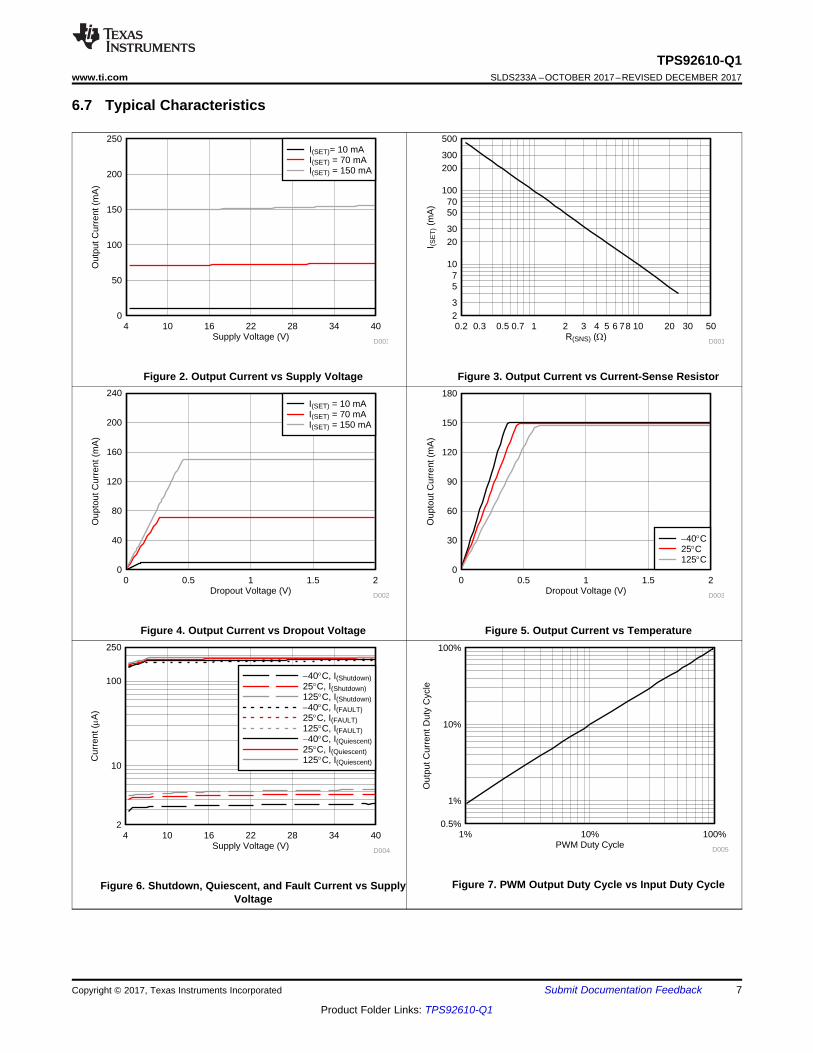
6.7 Typical Characteristics
Figure 2. Output Current vs Supply Voltage Figure 3. Output Current vs Current-Sense Resistor
Figure 4. Output Current vs Dropout Voltage Figure 5. Output Current vs Temperature
Figure 6. Shutdown, Quiescent, and Fault Current vs SupplyVoltage
Figure 7. PWM Output Duty Cycle vs Input Duty Cycle

8
TPS92610-Q1SLDS233A –OCTOBER 2017–REVISED DECEMBER 2017 www.ti.com
Product Folder Links: TPS92610-Q1
Submit Documentation Feedback Copyright © 2017, Texas Instruments Incorporated
Typical Characteristics (continued)
Ch. 1 = V(OUT) Ch. 2 = V(PWM) Ch. 4 = I(OUT)ƒ(PWM) = 200 Hz Duty cycle = 50%
Figure 8. PWM Dimming via External Input
Ch. 1 = V(SUPPLY) Ch. 2 = V(OUT) Ch. 3 = FAULTCh. 4 = I(OUT) f(PWM) = 1000 Hz Duty cycle = 30%
SUPPLY dimming between 2.5 V and 12 V FAULT floating
Figure 9. PWM Dimming via Power Supply
Ch. 1 = SUPPLY Ch. 2 = V(OUT) Ch. 3 = FAULTCh. 4 = I(OUT)
Figure 10. Transient Undervoltage
Ch. 1 = SUPPLY Ch. 2 = V(OUT) Ch. 3 = FAULTCh. 4 = I(OUT)
Figure 11. Transient Overvoltage
Ch. 1 = SUPPLY Ch. 2 = V(OUT) Ch. 3 = FAULTCh. 4 = I(OUT)
Figure 12. Jump Start
Ch. 1 = SUPPLY Ch. 2 = V(OUT) Ch. 3 = FAULTCh. 4 = I(OUT)
Figure 13. Superimposed Alternating Voltage, 15 Hz
9
TPS92610-Q1www.ti.com SLDS233A –OCTOBER 2017–REVISED DECEMBER 2017
Product Folder Links: TPS92610-Q1
Submit Documentation FeedbackCopyright © 2017, Texas Instruments Incorporated
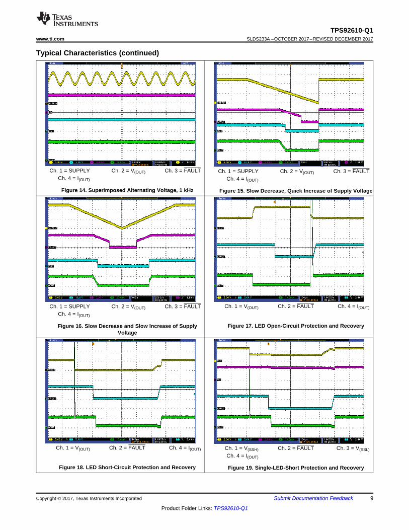
Typical Characteristics (continued)
Ch. 1 = SUPPLY Ch. 2 = V(OUT) Ch. 3 = FAULTCh. 4 = I(OUT)
Figure 14. Superimposed Alternating Voltage, 1 kHz
Ch. 1 = SUPPLY Ch. 2 = V(OUT) Ch. 3 = FAULTCh. 4 = I(OUT)
Figure 15. Slow Decrease, Quick Increase of Supply Voltage
Ch. 1 = SUPPLY Ch. 2 = V(OUT) Ch. 3 = FAULTCh. 4 = I(OUT)
Figure 16. Slow Decrease and Slow Increase of SupplyVoltage
Ch. 1 = V(OUT) Ch. 2 = FAULT Ch. 4 = I(OUT)
Figure 17. LED Open-Circuit Protection and Recovery
Ch. 1 = V(OUT) Ch. 2 = FAULT Ch. 4 = I(OUT)
Figure 18. LED Short-Circuit Protection and Recovery
Ch. 1 = V(SSH) Ch. 2 = FAULT Ch. 3 = V(SSL)Ch. 4 = I(OUT)
Figure 19. Single-LED-Short Protection and Recovery
Supply &
Control
LED Diagnostics
+ ±
Output Driver
SUPPLY
EN
DIAGEN
PWM
FAULT
GND
IN
OUT
SSH
SSL
TPS92610-Q1
Copyright ©2017, Texas Instruments Incorporated
R(SNS)
10
TPS92610-Q1SLDS233A –OCTOBER 2017–REVISED DECEMBER 2017 www.ti.com
Product Folder Links: TPS92610-Q1
Submit Documentation Feedback Copyright © 2017, Texas Instruments Incorporated
7 Detailed Description
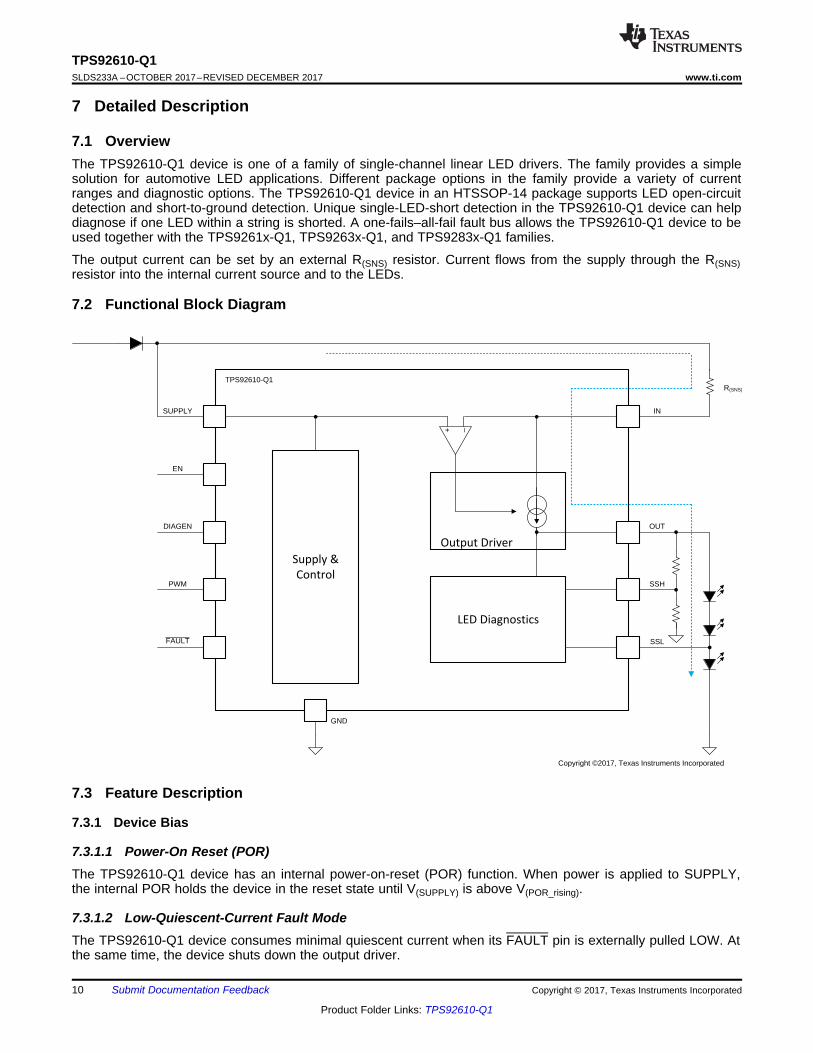
7.1 OverviewThe TPS92610-Q1 device is one of a family of single-channel linear LED drivers. The family provides a simplesolution for automotive LED applications. Different package options in the family provide a variety of currentranges and diagnostic options. The TPS92610-Q1 device in an HTSSOP-14 package supports LED open-circuitdetection and short-to-ground detection. Unique single-LED-short detection in the TPS92610-Q1 device can helpdiagnose if one LED within a string is shorted. A one-fails–all-fail fault bus allows the TPS92610-Q1 device to beused together with the TPS9261x-Q1, TPS9263x-Q1, and TPS9283x-Q1 families.
The output current can be set by an external R(SNS) resistor. Current flows from the supply through the R(SNS)resistor into the internal current source and to the LEDs.
7.2 Functional Block Diagram
7.3 Feature Description
7.3.1 Device Bias
7.3.1.1 Power-On Reset (POR)The TPS92610-Q1 device has an internal power-on-reset (POR) function. When power is applied to SUPPLY,the internal POR holds the device in the reset state until V(SUPPLY) is above V(POR_rising).
7.3.1.2 Low-Quiescent-Current Fault ModeThe TPS92610-Q1 device consumes minimal quiescent current when its FAULT pin is externally pulled LOW. Atthe same time, the device shuts down the output driver.

(CS _REG)(OUT)
(SNS)
VI
R
11
TPS92610-Q1www.ti.com SLDS233A –OCTOBER 2017–REVISED DECEMBER 2017
Product Folder Links: TPS92610-Q1
Submit Documentation FeedbackCopyright © 2017, Texas Instruments Incorporated
Feature Description (continued)If device detects an internal fault, it pulls the FAULT output LOW with constant current to signal a fault alarm onthe one-fails–all-fail fault bus.
7.3.2 Constant-Current DriverThe TPS92610-Q1 device has a high-side constant-current integrated driver. The device senses channel currentwith an external high-side current-sense resistor, R(SNS). A current regulation loop drives an internal transistorand regulates the current-sense voltage at the current-sense resistor to V(CS_REG). When the output driver is inregulation, the output current can be set using the following equation.
(1)
7.3.3 Device EnableThe TPS92610-Q1 device has an enable input, EN. When EN is low, the device is in sleep mode with ultralowquiescent current I(Shutdown). This low current helps to save system-level current consumption in applicationswhere battery voltage directly connects to the device without high-side switches.
7.3.4 PWM DimmingThe TPS92610-Q1 device supports PWM output dimming via PWM input dimming and supply dimming.
The PWM input functions as an enable for the output current. When the PWM input is low, the device alsodisables the diagnostic features.
Supply dimming applies PWM dimming on the power input. For an accurate PWM threshold, TI recommendsusing a resistor divider on the PWM input to set the PWM threshold higher than V(POR_rising).
7.3.5 DiagnosticsThe TPS92610-Q1 device provides advanced diagnostics and fault protection features for automotive exteriorlighting systems. The device is able to detect and protect from LED string short-to-GND, LED string open-circuit,and single-LED-short scenarios. It also supports a one-fails–all-fail fault bus that could flexibly fit differentlegislative requirements.
7.3.5.1 DIAGENThe TPS92610-Q1 device supports the DIAGEN pin with an accurate threshold to disable the open-circuit andsingle-LED-short diagnostic functions. With a resistor divider, the DIAGEN pin can be used to sense SUPPLYvoltage with a resistor-programmable threshold. With the DIAGEN feature, the device is able to avoid false errorreports due to low-dropout voltage and to drive maximum current in low-dropout mode when the input voltage isnot high enough for current regulation.
When V(DIAGEN) is higher than the threshold VIH(DIAGEN), the device enables LED open-circuit and single-LED-shortdiagnostics. When V(DIAGEN) is lower than the threshold VIL(DIAGEN), the device disables LED-open-circuit andsingle-LED-short diagnostics.
7.3.5.2 Low-Dropout ModeWhen the supply voltage drops, the TPS92610-Q1 device tries to regulate current by driving internal transistorsin the linear region, also known as low-dropout mode, because the voltage across the sense resistor fails toreach the regulation target.
In low-dropout mode, the open-circuit diagnostic must be disabled. Otherwise, the device treats the low-dropoutmode as an open-circuit fault. The DIAGEN pin is used to avoid false diagnostics on the output channel due tolow supply voltage.
When the DIAGEN voltage is low, single-LED short- and open-circuit detection is ignored. When the DIAGENvoltage is high, single-LED short- and open-circuit detection return to normal operation.
In dropout mode, a diode in parallel with the sense resistor is recommended to clamp the voltage betweenSUPPLY and IN (across the sense resistor) in case of a large current pulse during recovery.

SSH
OUT
R2
R1
+
–
+
–
SSLV – V > VSSL SSH (SSH_th)
V < VSSL (SSL_th)
V(SSL_th)
Copyright © 2017, Texas Instruments Incorporated
12
TPS92610-Q1SLDS233A –OCTOBER 2017–REVISED DECEMBER 2017 www.ti.com
Product Folder Links: TPS92610-Q1
Submit Documentation Feedback Copyright © 2017, Texas Instruments Incorporated
Feature Description (continued)7.3.5.3 Open-Circuit DetectionThe TPS92610-Q1 device has LED open-circuit detection. Open-circuit detection monitors the output voltagewhen the channel is in the ON state. Open-circuit detection is only enabled when DIAGEN is HIGH. A short-to-battery fault is also detected as an LED open-circuit fault.
The device monitors dropout-voltage differences between the IN and OUT pins when PWM is HIGH. The voltagedifference V(IN) – V(OUT) is compared with the internal reference voltage V(OPEN_th_rising) to detect an LED open-circuit failure. If V(IN) – V(OUT) falls below the V(OPEN_th_rising) voltage longer than the deglitch time of t(OPEN_deg), thedevice asserts an open-circuit fault. Once an LED open-circuit failure is detected, the constant-current sourcepulls the fault bus down. During the deglitch time period, if V(IN) – V(OUT) rises above V(OPEN_th_falling), the deglitchtimer is reset.
When the device is in auto-retry, the device keeps the output ON to retry if the PWM input is HIGH; the devicesources a small current I(retry) from IN to OUT when PWM input is LOW. In either scenario, once a faulty channelrecovers, the device resumes normal operation and releases the FAULT pulldown.
7.3.5.4 Short-to-GND DetectionThe TPS92610-Q1 device has LED short-to-GND detection. Short-to-GND detection monitors the output voltagewhen the channel is in the ON state. Once a short-to-GND LED failure is detected, the device turns off the outputchannel and retries automatically, ignoring the PWM input. If the retry mechanism detects removal of the LEDshort-to-GND fault, the device resumes normal operation.
The device monitors the V(OUT) voltage and compares it with the internal reference voltage to detect a short-to-GND failure. If V(OUT) falls below V(SG_th_rising) longer than the deglitch time of t(SG_deg), the device asserts theshort-to-GND fault and pulls FAULT low. During the deglitching time period, if V(OUT) rises above V(SG_th_falling), thetimer is reset.
Once the device has asserted a short-to-GND fault, the device turns OFF the output channel and retriesautomatically with a small current. When retrying, the device sources a small current I(retry) from IN to OUT to pullup the LED loads continuously. Once auto-retry detects output voltage rising above V(SG_th_falling), it clears theshort-to-GND fault and resumes normal operation.
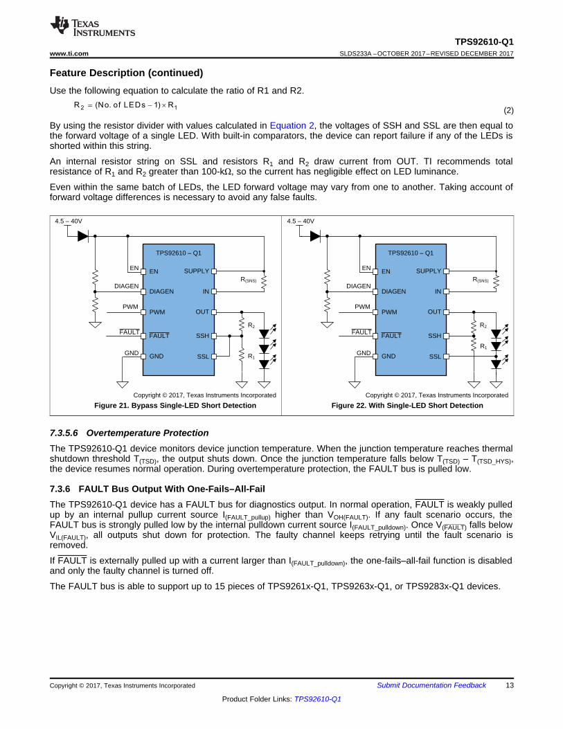
7.3.5.5 Single-LED-Short DetectionThe TPS92610-Q1 device supports single-LED-short detection by using the SSH and SSL pins. In case there isno need of this feature, SSH and SSL must be tied together to a resistor divider to avoid false alarms as shownin Figure 21.
The TPS92610-Q1 device has integrated a precision comparator to monitor a single-LED-short failure. Thecomparator uses the bottom LED forward voltage V(SSL) as a reference and monitors the string voltage V(OUT)with resistor divider R1 and R2 at V(SSH).
If a single-LED short is detected, the device turns off the output channel and retries with a small current I(RETRY).Once the fault is removed, the device automatically resumes normal operation.
Figure 20. Single-LED Short Detection
EN
OUT
SSH
TPS92610 ± Q1
SUPPLY
4.5 ± 40V
R(SNS)
SSLGNDGND
EN
DIAGENDIAGEN
PWMPWM
IN
FAULT FAULT
Copyright © 2017, Texas Instruments Incorporated
R2
R1
EN
OUT
SSH
TPS92610 ± Q1
SUPPLY
4.5 ± 40V
R(SNS)
SSLGNDGND
EN
DIAGENDIAGEN
PWMPWM
IN
FAULT FAULT
Copyright © 2017, Texas Instruments Incorporated
R2
R1
2 1R (No. of LEDs 1) R= - ´
13
TPS92610-Q1www.ti.com SLDS233A –OCTOBER 2017–REVISED DECEMBER 2017
Product Folder Links: TPS92610-Q1
Submit Documentation FeedbackCopyright © 2017, Texas Instruments Incorporated
Feature Description (continued)Use the following equation to calculate the ratio of R1 and R2.
(2)
By using the resistor divider with values calculated in Equation 2, the voltages of SSH and SSL are then equal tothe forward voltage of a single LED. With built-in comparators, the device can report failure if any of the LEDs isshorted within this string.
An internal resistor string on SSL and resistors R1 and R2 draw current from OUT. TI recommends totalresistance of R1 and R2 greater than 100-kΩ, so the current has negligible effect on LED luminance.
Even within the same batch of LEDs, the LED forward voltage may vary from one to another. Taking account offorward voltage differences is necessary to avoid any false faults.
Figure 21. Bypass Single-LED Short Detection Figure 22. With Single-LED Short Detection
7.3.5.6 Overtemperature ProtectionThe TPS92610-Q1 device monitors device junction temperature. When the junction temperature reaches thermalshutdown threshold T(TSD), the output shuts down. Once the junction temperature falls below T(TSD) – T(TSD_HYS),the device resumes normal operation. During overtemperature protection, the FAULT bus is pulled low.
7.3.6 FAULT Bus Output With One-Fails–All-FailThe TPS92610-Q1 device has a FAULT bus for diagnostics output. In normal operation, FAULT is weakly pulledup by an internal pullup current source I(FAULT_pullup) higher than VOH(FAULT). If any fault scenario occurs, theFAULT bus is strongly pulled low by the internal pulldown current source I(FAULT_pulldown). Once V(FAULT) falls belowVIL(FAULT), all outputs shut down for protection. The faulty channel keeps retrying until the fault scenario isremoved.
If FAULT is externally pulled up with a current larger than I(FAULT_pulldown), the one-fails–all-fail function is disabledand only the faulty channel is turned off.
The FAULT bus is able to support up to 15 pieces of TPS9261x-Q1, TPS9263x-Q1, or TPS9283x-Q1 devices.

14
TPS92610-Q1SLDS233A –OCTOBER 2017–REVISED DECEMBER 2017 www.ti.com
Product Folder Links: TPS92610-Q1
Submit Documentation Feedback Copyright © 2017, Texas Instruments Incorporated
Feature Description (continued)Table 1. Fault Table With DIAGEN = HIGH
FAULT BUSSTATUS
FAULT TYPE DETECTIONMECHANISM
CHANNELSTATE
DEGLITCHTIME
FAULT BUS FAULTHANDLINGROUTINE
FAULTRECOVERY
FAULT floatingor externallypulled up
Open-circuit orshort-to-supply
V(IN) – V(OUT) <V(OPEN_th_rising)
On t(OPEN_deg) Constant-currentpulldown
Device worksnormally withFAULT pinpulled low.Device sourcesI(retry) currentwhen PWM isLOW. Devicekeeps outputnormal whenPWM is HIGH.
Auto recover
Short-to-ground V(OUT) <V(SG_th_rising)
On t(SG_deg) Constant-currentpulldown
Device turnsoutput off andretries withconstantcurrent I(retry),ignoring thePWM input.
Auto recover
Single-LEDshort
V(SSL) – V(SSH)> V(SS_th) orV(SSL) <V(SSL_th)
On t(SS_deg) Constant-currentpulldown
Device turnsoutput off andretry withconstantcurrent I(retry),ignoring thePWM input.
Auto recover
Overtemperature
TJ > T(TSD) On or off t(TSD_deg) Constant-currentpulldown
Devices turnsoutput off.
Auto recover
Externallypulled low
Device turns output off
Table 2. Fault Table With DIAGEN = LOWFAULT BUS
STATUSFAULT TYPE DETECTION
MECHANISMCHANNEL
STATEDEGLITCH
TIMEFAULT BUS FAULT
HANDLINGROUTINE
FAULTRECOVERY
FAULT floatingor externallypulled up
Open-circuit orshort-to-supply
Ignored
Short-to-ground VOUT <V(SG_th_rising)
On t(SG_deg) Constant-currentpulldown
Device turnsoutput off andretries withconstantcurrent I(retry),ignoring thePWM input.
Auto recover
Single-LEDshort
Ignored
Overtemperature
TJ > T(TSD) On or off t(TSD_deg) Constant-currentpulldown
Device turnsoutput off.
Auto recover
Externallypulled low
Device turns output off
7.4 Device Functional Modes
7.4.1 Undervoltage Lockout, V(SUPPLY)<V(POR_rising)
When the device is in undervoltage lockout mode, the TPS92610-Q1 device disables all functions until the supplyrises above the UVLO-rising threshold.
15
TPS92610-Q1www.ti.com SLDS233A –OCTOBER 2017–REVISED DECEMBER 2017
Product Folder Links: TPS92610-Q1
Submit Documentation FeedbackCopyright © 2017, Texas Instruments Incorporated
Device Functional Modes (continued)7.4.2 Normal Operation V(SUPPLY) ≥ 4.5 VThe device drives an LED string in normal operation. With enough voltage drop across SUPPLY and OUT, thedevice is able to drive the output in constant-current mode.
7.4.3 Low-Voltage DropoutWhen the device drives an LED string in low-dropout mode, if the voltage drop is less than open-circuit detectionthreshold, the device may report a false open-circuit fault. Set the DIAGEN threshold higher than LED stringvoltage to avoid a false open-circuit detection.
7.4.4 Fault ModeWhen the device detects an open circuit or a shorted LED, the device tries to pull down the FAULT pin with aconstant current. If the FAULT bus is pulled down, the device switches to fault mode and consumes a faultcurrent of I(FAULT).

(CS _REG)(SNS)
(LED)
RR 1.96
I= = W
EN
OUT
SSH
TPS92610 ± Q1
SUPPLY
SUPPLY
R(SNS)
SSLGNDGND
EN
DIAGENDIAGEN
PWMPWM
IN
FAULT FAULT
Copyright © 2017, Texas Instruments Incorporated
I(LED)
R2
R1
R4
R3
16
TPS92610-Q1SLDS233A –OCTOBER 2017–REVISED DECEMBER 2017 www.ti.com
Product Folder Links: TPS92610-Q1
Submit Documentation Feedback Copyright © 2017, Texas Instruments Incorporated
8 Application and Implementation
NOTEInformation in the following applications sections is not part of the TI componentspecification, and TI does not warrant its accuracy or completeness. TI’s customers areresponsible for determining suitability of components for their purposes. Customers shouldvalidate and test their design implementation to confirm system functionality.
8.1 Application InformationIn automotive lighting applications, thermal performance and LED diagnostics are always design challenges forlinear LED drivers.
The TPS92610-Q1 device is capable of detecting LED open-circuit, LED short-circuit and single-LED shortfailures. To increase current-driving capability, the TPS92610-Q1 device supports using an external a parallelresistor to help dissipate heat as shown in the following application, Figure 25. This technique provides the low-cost solution of using external resistors to dissipate heat due to high input voltage, and still keeps high accuracyof the total current output. Note that the one-fails–all-fail feature is not supported by this topology.
8.2 Typical Application
8.2.1 Single-Channel LED Driver With Full DiagnosticsThe TPS92610-Q1 device is a potential choice for LED driver for applications with diagnostics requirements. Inmany cases, single-LED short diagnostics are mandatory for applications such as sequential turn indicators.
Figure 23. Typical Application Diagram
8.2.1.1 Design RequirementsInput voltage ranges from 9 V to 16 V, LED maximum forward voltage Vfmax = 2.5 V, minimum forward voltageVfmin = 1.9 V, current I(LED) = 50 mA.
8.2.1.2 Detailed Design ProcedureCurrent setting by sense resistor is as described inEquation 1.
(3)
LED-string maximum forward voltage = 3 × 2.5 V = 7.5 V.
(Max) (SUPPLY) (CS _REG) (OUT) (LED) (SUPPLY) (Quiescent)P (V V V ) I V I
(16 3 1.9 0.098) 0.05 16 0.00025 0.5141 W
= - - ´ + ´
= - ´ - ´ + ´ =
2
1
R= 2
R
3IL(DIAG,min)
3 4
7.9 RV
R R
´
=
+
17
TPS92610-Q1www.ti.com SLDS233A –OCTOBER 2017–REVISED DECEMBER 2017
Product Folder Links: TPS92610-Q1
Submit Documentation FeedbackCopyright © 2017, Texas Instruments Incorporated
Typical Application (continued)With 400-mV headroom reserved for the TPS92610-Q1 device between SUPPLY and OUT, the TPS92610-Q1device must disable open-circuit detection when the supply voltage is below 7.9 V by using the DIAGEN feature.
(4)
Set R4 = 10 kΩ, R3 = 65.6 kΩ.
The single-LED short-detection resistor ratio can be calculated as follows.
(5)
If R1 = 50 kΩ, R2 = 100 kΩ
Total device power consumption at worst case is with 16-V input and LEDs at minimal froward voltage.
(6)
8.2.1.3 Application Curve
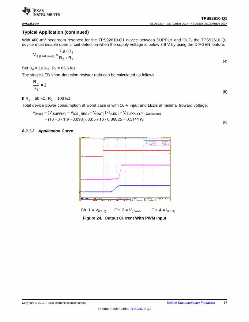
Ch. 1 = V(OUT) Ch. 2 = V(PWM) Ch. 4 = I(OUT)
Figure 24. Output Current With PWM Input
(CS _REG)(SNS)
(LED)
RR 0.49
I= = W
EN
OUT
SSH
TPS92610 ± Q1
SUPPLY
SUPPLY
R(SNS)
SSLGNDGND
EN
DIAGENDIAGEN
PWMPWM
IN
FAULT FAULT
R(P)
Copyright © 2017, Texas Instruments Incorporated
I(P)
I(DRIVE)I(LED)
18
TPS92610-Q1SLDS233A –OCTOBER 2017–REVISED DECEMBER 2017 www.ti.com
Product Folder Links: TPS92610-Q1
Submit Documentation Feedback Copyright © 2017, Texas Instruments Incorporated
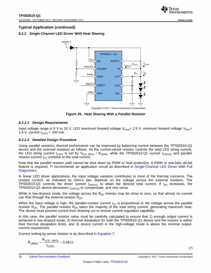
Typical Application (continued)8.2.2 Single-Channel LED Driver With Heat Sharing
Figure 25. Heat Sharing With a Parallel Resistor
8.2.2.1 Design RequirementsInput voltage range is 9 V to 16 V, LED maximum forward voltage Vfmax= 2.5 V, minimum forward voltage Vfmin=1.9 V, current I(LED) = 200 mA.
8.2.2.2 Detailed Design ProcedureUsing parallel resistors, thermal performance can be improved by balancing current between the TPS92610-Q1device and the external resistors as follows. As the current-sense resistor controls the total LED string current,the LED string current I(LED) is set by V(CS_REG) / R(SNS), while the TPS92610-Q1 current I(DRIVE) and parallelresistor current I(P) combine to the total current.
Note that the parallel resistor path cannot be shut down by PWM or fault protection. If PWM or one-fails–all-failfeature is required, TI recommends an application circuit as described in Single-Channel LED Driver With FullDiagnostics.
In linear LED driver applications, the input voltage variation contributes to most of the thermal concerns. Theresistor current, as indicated by Ohm’s law, depends on the voltage across the external resistors. TheTPS92610-Q1 controls the driver current I(DRIVE) to attain the desired total current. If I(P) increases, theTPS92610-Q1 device decreases I(DRIVE) to compensate, and vice versa.
While in low-dropout mode, the voltage across the R(P) resistor may be close to zero, so that almost no currentcan flow through the external resistor R(P).
When the input voltage is high, the parallel-resistor current I(P) is proportional to the voltage across the parallelresistor R(P). The parallel resistor R(P) takes the majority of the total string current, generating maximum heat.The device must prevent current from draining out to ensure current regulation capability.
In this case, the parallel resistor value must be carefully calculated to ensure that 1) enough output current isachieved in low-dropout mode, 2) thermal dissipation for both the TPS92610-Q1 device and the resistor is withintheir thermal dissipation limits, and 3) device current in the high-voltage mode is above the minimal output-current requirement.
Current setting by sense resistor is as described in Equation 7.
(7)

� � � �2 2
(SUPPLY) (CS _REG) (OUT)(RP _MAX)
(P)
V V V 16 3 1.9 0.098P 1.04W
R 100
� � � u �
(SUPPLY) (CS _ REG) (OUT)(DEV _ MAX) (SUPPLY) (CS _ REG) (OUT) (LED) (SUPPLY) (Quiescent)
(P)
V V VP (V V V ) I V I
R
(16 3 1.9 0.098) 0.1 16 0.00025 1.0242 W
æ ö- -= - - ´ - + ´ç ÷
ç ÷è ø
= - ´ - ´ + ´ =
(SUPPLY) (CS _REG) (OUT)(P)
(LED)
V V V 16 3 1.9 0.098R 100
0.5 I 0.5 0.2
� � � u � | :
u u
19
TPS92610-Q1www.ti.com SLDS233A –OCTOBER 2017–REVISED DECEMBER 2017
Product Folder Links: TPS92610-Q1
Submit Documentation FeedbackCopyright © 2017, Texas Instruments Incorporated
Typical Application (continued)LED-string maximum forward voltage = 3 × 2.5 V = 7.5 V.
Parallel resistor R(P) is recommended to consume 50% of the total current at maximum supply voltage.
(8)
Total device power consumption is maximum at 16 V input and LED minimal forward voltage.
(9)
Resistor R(P) maximum power consumption is at 16-V input.
(10)
Users must consider the maximum power of both of the device and the parallel resistor.
8.2.2.3 Application Curve
Ch. 1 = V(SUPPLY) Ch. 2 = V(OUT) Ch. 3 = I(P)
Ch. 4 = I(LED) V(SUPPLY) increases from 9 V to 16 V
Figure 26. Constant Output Current With Increasing Supply Voltage
4
3
2
1
5
7
6
13
10
9
8
11
12
14
GND
FAULT
SSL
PWM
NC
NC
IN
NC
OUT
NC
SUPPLYEN
SSH
DIAGEN
GND
IN
TPS92610-Q1
SUPPLY
Copyright © 2017, Texas Instruments Incorporated
20
TPS92610-Q1SLDS233A –OCTOBER 2017–REVISED DECEMBER 2017 www.ti.com
Product Folder Links: TPS92610-Q1
Submit Documentation Feedback Copyright © 2017, Texas Instruments Incorporated
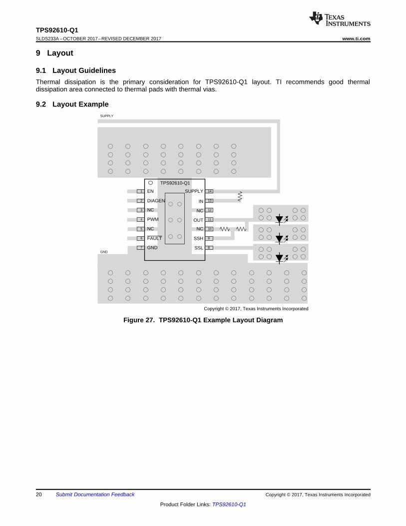
9 Layout
9.1 Layout GuidelinesThermal dissipation is the primary consideration for TPS92610-Q1 layout. TI recommends good thermaldissipation area connected to thermal pads with thermal vias.
9.2 Layout Example
Figure 27. TPS92610-Q1 Example Layout Diagram
21
TPS92610-Q1www.ti.com SLDS233A –OCTOBER 2017–REVISED DECEMBER 2017
Product Folder Links: TPS92610-Q1
Submit Documentation FeedbackCopyright © 2017, Texas Instruments Incorporated
10 Device and Documentation Support
10.1 Documentation Support
10.1.1 Related DocumentationFor related documentation see the following:• TPS92610-Q1 EVM User's Guide• How to Calculate TPS92630-Q1 Maximum Output Current for Automotive Exterior Lighting Applications• Automotive Linear LED Driver Reference Design for Center High-Mounted Stop Lamp (CHMSL)• User Guides: Automotive Linear LED Driver Reference Design for Center High-Mounted Stop Lamp (CHMSL)
10.2 Receiving Notification of Documentation UpdatesTo receive notification of documentation updates, navigate to the device product folder on ti.com. In the upperright corner, click on Alert me to register and receive a weekly digest of any product information that haschanged. For change details, review the revision history included in any revised document.
10.3 Community ResourcesThe following links connect to TI community resources. Linked contents are provided "AS IS" by the respectivecontributors. They do not constitute TI specifications and do not necessarily reflect TI's views; see TI's Terms ofUse.
TI E2E™ Online Community TI's Engineer-to-Engineer (E2E) Community. Created to foster collaborationamong engineers. At e2e.ti.com, you can ask questions, share knowledge, explore ideas and helpsolve problems with fellow engineers.
Design Support TI's Design Support Quickly find helpful E2E forums along with design support tools andcontact information for technical support.
10.4 TrademarksPowerPAD, E2E are trademarks of Texas Instruments.All other trademarks are the property of their respective owners.
10.5 Electrostatic Discharge CautionThis integrated circuit can be damaged by ESD. Texas Instruments recommends that all integrated circuits be handled withappropriate precautions. Failure to observe proper handling and installation procedures can cause damage.
ESD damage can range from subtle performance degradation to complete device failure. Precision integrated circuits may be moresusceptible to damage because very small parametric changes could cause the device not to meet its published specifications.
10.6 GlossarySLYZ022 — TI Glossary.
This glossary lists and explains terms, acronyms, and definitions.
22
TPS92610-Q1SLDS233A –OCTOBER 2017–REVISED DECEMBER 2017 www.ti.com
Product Folder Links: TPS92610-Q1
Submit Documentation Feedback Copyright © 2017, Texas Instruments Incorporated
11 Mechanical, Packaging, and Orderable InformationThe following pages include mechanical, packaging, and orderable information. This information is the most-current data available for the designated device. This data is subject to change without notice and withoutrevision of this document. For browser-based versions of this data sheet, see the left-hand navigation pane.
PACKAGE OPTION ADDENDUM
www.ti.com 28-Dec-2017
Addendum-Page 1
PACKAGING INFORMATION
Orderable Device Status(1)
Package Type PackageDrawing
Pins PackageQty
Eco Plan(2)
Lead/Ball Finish(6)
MSL Peak Temp(3)
Op Temp (°C) Device Marking(4/5)
Samples
TPS92610QPWPRQ1 ACTIVE HTSSOP PWP 14 2000 Green (RoHS& no Sb/Br)
CU NIPDAU Level-3-260C-168 HR -40 to 125 TP92610
(1) The marketing status values are defined as follows:ACTIVE: Product device recommended for new designs.LIFEBUY: TI has announced that the device will be discontinued, and a lifetime-buy period is in effect.NRND: Not recommended for new designs. Device is in production to support existing customers, but TI does not recommend using this part in a new design.PREVIEW: Device has been announced but is not in production. Samples may or may not be available.OBSOLETE: TI has discontinued the production of the device.
(2) RoHS: TI defines "RoHS" to mean semiconductor products that are compliant with the current EU RoHS requirements for all 10 RoHS substances, including the requirement that RoHS substancedo not exceed 0.1% by weight in homogeneous materials. Where designed to be soldered at high temperatures, "RoHS" products are suitable for use in specified lead-free processes. TI mayreference these types of products as "Pb-Free".RoHS Exempt: TI defines "RoHS Exempt" to mean products that contain lead but are compliant with EU RoHS pursuant to a specific EU RoHS exemption.Green: TI defines "Green" to mean the content of Chlorine (Cl) and Bromine (Br) based flame retardants meet JS709B low halogen requirements of <=1000ppm threshold. Antimony trioxide basedflame retardants must also meet the <=1000ppm threshold requirement.
(3) MSL, Peak Temp. - The Moisture Sensitivity Level rating according to the JEDEC industry standard classifications, and peak solder temperature.
(4) There may be additional marking, which relates to the logo, the lot trace code information, or the environmental category on the device.
(5) Multiple Device Markings will be inside parentheses. Only one Device Marking contained in parentheses and separated by a "~" will appear on a device. If a line is indented then it is a continuationof the previous line and the two combined represent the entire Device Marking for that device.
(6) Lead/Ball Finish - Orderable Devices may have multiple material finish options. Finish options are separated by a vertical ruled line. Lead/Ball Finish values may wrap to two lines if the finishvalue exceeds the maximum column width.
Important Information and Disclaimer:The information provided on this page represents TI's knowledge and belief as of the date that it is provided. TI bases its knowledge and belief on informationprovided by third parties, and makes no representation or warranty as to the accuracy of such information. Efforts are underway to better integrate information from third parties. TI has taken andcontinues to take reasonable steps to provide representative and accurate information but may not have conducted destructive testing or chemical analysis on incoming materials and chemicals.TI and TI suppliers consider certain information to be proprietary, and thus CAS numbers and other limited information may not be available for release.
In no event shall TI's liability arising out of such information exceed the total purchase price of the TI part(s) at issue in this document sold by TI to Customer on an annual basis.
TAPE AND REEL INFORMATION
*All dimensions are nominal
Device PackageType
PackageDrawing
Pins SPQ ReelDiameter
(mm)
ReelWidth
W1 (mm)
A0(mm)
B0(mm)
K0(mm)
P1(mm)
W(mm)
Pin1Quadrant
TPS92610QPWPRQ1 HTSSOP PWP 14 2000 330.0 12.4 6.9 5.6 1.6 8.0 12.0 Q1
PACKAGE MATERIALS INFORMATION
www.ti.com 16-Dec-2017
Pack Materials-Page 1
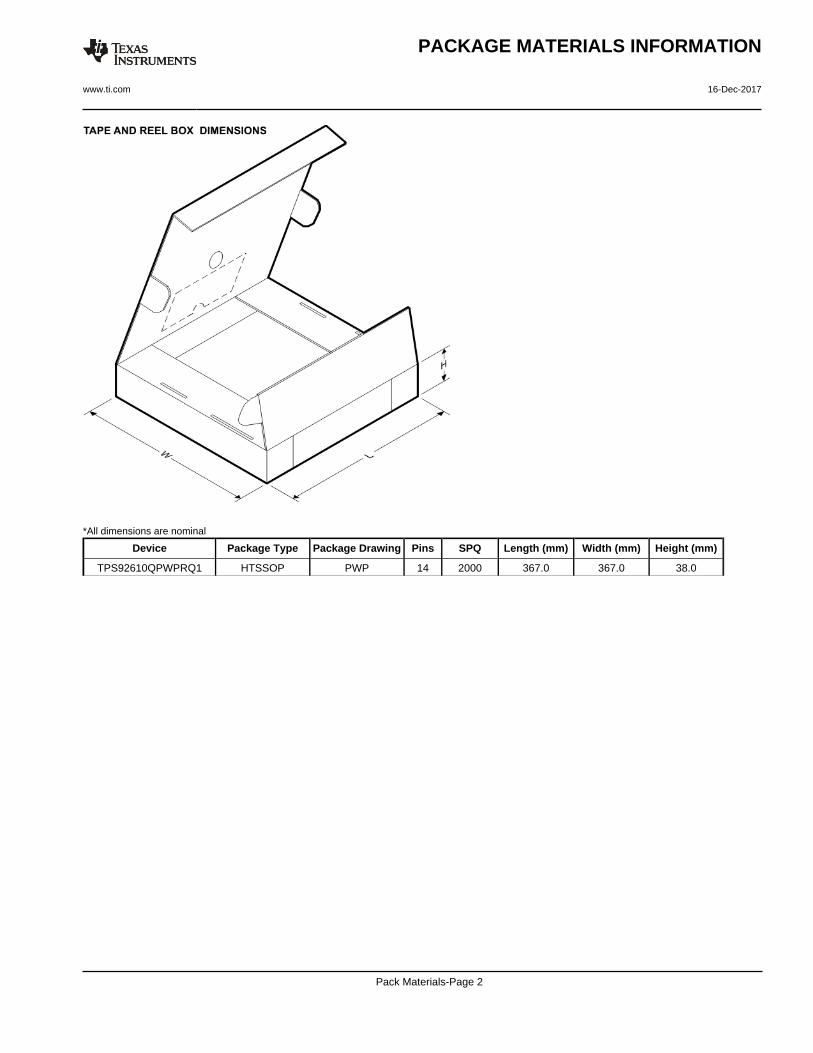
*All dimensions are nominal
Device Package Type Package Drawing Pins SPQ Length (mm) Width (mm) Height (mm)
TPS92610QPWPRQ1 HTSSOP PWP 14 2000 367.0 367.0 38.0
PACKAGE MATERIALS INFORMATION
www.ti.com 16-Dec-2017
Pack Materials-Page 2


IMPORTANT NOTICE
Texas Instruments Incorporated (TI) reserves the right to make corrections, enhancements, improvements and other changes to itssemiconductor products and services per JESD46, latest issue, and to discontinue any product or service per JESD48, latest issue. Buyersshould obtain the latest relevant information before placing orders and should verify that such information is current and complete.TI’s published terms of sale for semiconductor products (http://www.ti.com/sc/docs/stdterms.htm) apply to the sale of packaged integratedcircuit products that TI has qualified and released to market. Additional terms may apply to the use or sale of other types of TI products andservices.Reproduction of significant portions of TI information in TI data sheets is permissible only if reproduction is without alteration and isaccompanied by all associated warranties, conditions, limitations, and notices. TI is not responsible or liable for such reproduceddocumentation. Information of third parties may be subject to additional restrictions. Resale of TI products or services with statementsdifferent from or beyond the parameters stated by TI for that product or service voids all express and any implied warranties for theassociated TI product or service and is an unfair and deceptive business practice. TI is not responsible or liable for any such statements.Buyers and others who are developing systems that incorporate TI products (collectively, “Designers”) understand and agree that Designersremain responsible for using their independent analysis, evaluation and judgment in designing their applications and that Designers havefull and exclusive responsibility to assure the safety of Designers' applications and compliance of their applications (and of all TI productsused in or for Designers’ applications) with all applicable regulations, laws and other applicable requirements. Designer represents that, withrespect to their applications, Designer has all the necessary expertise to create and implement safeguards that (1) anticipate dangerousconsequences of failures, (2) monitor failures and their consequences, and (3) lessen the likelihood of failures that might cause harm andtake appropriate actions. Designer agrees that prior to using or distributing any applications that include TI products, Designer willthoroughly test such applications and the functionality of such TI products as used in such applications.TI’s provision of technical, application or other design advice, quality characterization, reliability data or other services or information,including, but not limited to, reference designs and materials relating to evaluation modules, (collectively, “TI Resources”) are intended toassist designers who are developing applications that incorporate TI products; by downloading, accessing or using TI Resources in anyway, Designer (individually or, if Designer is acting on behalf of a company, Designer’s company) agrees to use any particular TI Resourcesolely for this purpose and subject to the terms of this Notice.TI’s provision of TI Resources does not expand or otherwise alter TI’s applicable published warranties or warranty disclaimers for TIproducts, and no additional obligations or liabilities arise from TI providing such TI Resources. TI reserves the right to make corrections,enhancements, improvements and other changes to its TI Resources. TI has not conducted any testing other than that specificallydescribed in the published documentation for a particular TI Resource.Designer is authorized to use, copy and modify any individual TI Resource only in connection with the development of applications thatinclude the TI product(s) identified in such TI Resource. NO OTHER LICENSE, EXPRESS OR IMPLIED, BY ESTOPPEL OR OTHERWISETO ANY OTHER TI INTELLECTUAL PROPERTY RIGHT, AND NO LICENSE TO ANY TECHNOLOGY OR INTELLECTUAL PROPERTYRIGHT OF TI OR ANY THIRD PARTY IS GRANTED HEREIN, including but not limited to any patent right, copyright, mask work right, orother intellectual property right relating to any combination, machine, or process in which TI products or services are used. Informationregarding or referencing third-party products or services does not constitute a license to use such products or services, or a warranty orendorsement thereof. Use of TI Resources may require a license from a third party under the patents or other intellectual property of thethird party, or a license from TI under the patents or other intellectual property of TI.TI RESOURCES ARE PROVIDED “AS IS” AND WITH ALL FAULTS. TI DISCLAIMS ALL OTHER WARRANTIES ORREPRESENTATIONS, EXPRESS OR IMPLIED, REGARDING RESOURCES OR USE THEREOF, INCLUDING BUT NOT LIMITED TOACCURACY OR COMPLETENESS, TITLE, ANY EPIDEMIC FAILURE WARRANTY AND ANY IMPLIED WARRANTIES OFMERCHANTABILITY, FITNESS FOR A PARTICULAR PURPOSE, AND NON-INFRINGEMENT OF ANY THIRD PARTY INTELLECTUALPROPERTY RIGHTS. TI SHALL NOT BE LIABLE FOR AND SHALL NOT DEFEND OR INDEMNIFY DESIGNER AGAINST ANY CLAIM,INCLUDING BUT NOT LIMITED TO ANY INFRINGEMENT CLAIM THAT RELATES TO OR IS BASED ON ANY COMBINATION OFPRODUCTS EVEN IF DESCRIBED IN TI RESOURCES OR OTHERWISE. IN NO EVENT SHALL TI BE LIABLE FOR ANY ACTUAL,DIRECT, SPECIAL, COLLATERAL, INDIRECT, PUNITIVE, INCIDENTAL, CONSEQUENTIAL OR EXEMPLARY DAMAGES INCONNECTION WITH OR ARISING OUT OF TI RESOURCES OR USE THEREOF, AND REGARDLESS OF WHETHER TI HAS BEENADVISED OF THE POSSIBILITY OF SUCH DAMAGES.Unless TI has explicitly designated an individual product as meeting the requirements of a particular industry standard (e.g., ISO/TS 16949and ISO 26262), TI is not responsible for any failure to meet such industry standard requirements.Where TI specifically promotes products as facilitating functional safety or as compliant with industry functional safety standards, suchproducts are intended to help enable customers to design and create their own applications that meet applicable functional safety standardsand requirements. Using products in an application does not by itself establish any safety features in the application. Designers mustensure compliance with safety-related requirements and standards applicable to their applications. Designer may not use any TI products inlife-critical medical equipment unless authorized officers of the parties have executed a special contract specifically governing such use.Life-critical medical equipment is medical equipment where failure of such equipment would cause serious bodily injury or death (e.g., lifesupport, pacemakers, defibrillators, heart pumps, neurostimulators, and implantables). Such equipment includes, without limitation, allmedical devices identified by the U.S. Food and Drug Administration as Class III devices and equivalent classifications outside the U.S.TI may expressly designate certain products as completing a particular qualification (e.g., Q100, Military Grade, or Enhanced Product).Designers agree that it has the necessary expertise to select the product with the appropriate qualification designation for their applicationsand that proper product selection is at Designers’ own risk. Designers are solely responsible for compliance with all legal and regulatoryrequirements in connection with such selection.Designer will fully indemnify TI and its representatives against any damages, costs, losses, and/or liabilities arising out of Designer’s non-compliance with the terms and provisions of this Notice.
Mailing Address: Texas Instruments, Post Office Box 655303, Dallas, Texas 75265Copyright © 2017, Texas Instruments Incorporated