transistor circuits for a mems based transceiver
TRANSCRIPT

Transistor Circuits For A MEMS Based Transceiver
Kelvin Liang
Electrical Engineering and Computer SciencesUniversity of California at Berkeley
Technical Report No. UCB/EECS-2015-48http://www.eecs.berkeley.edu/Pubs/TechRpts/2015/EECS-2015-48.html
May 7, 2015

Copyright © 2015, by the author(s).All rights reserved.
Permission to make digital or hard copies of all or part of this work forpersonal or classroom use is granted without fee provided that copies arenot made or distributed for profit or commercial advantage and thatcopies bear this notice and the full citation on the first page. To copyotherwise, to republish, to post on servers or to redistribute to lists,requires prior specific permission.

University of California, Berkeley College of Engineering
MASTER OF ENGINEERING - SPRING 2015
Electrical Engineering and Computer Science
Integrated Circuits
Transistor Circuits for a MEMS Based Transceiver
Kelvin Liang
This Masters Project Paper fulfills the Master of Engineering degree requirement.
Approved by:
1. Capstone Project Advisor:
Signature: __________________________ Date ____________
Print Name/Department: Clark T.-C. Nguyen / EECS
2. Faculty Committee Member #2:
Signature: __________________________ Date ____________
Print Name/Department: David J. Allstot / EECS
Page 2
Transistor Circuits for MEMS Based Transceiver
by
Kelvin Liang
A project report submitted in partial satisfaction of the
requirements for the degree of
Master of Engineering
in
Electrical Engineering and Computer Science
in the
GRADUATE DIVISION
of the
UNIVERSITY OF CALIFORNIA, BERKELEY
Committee in charge:
Professor Clark T.-C. Nguyen
Professor David J. Allstot
Spring 2015

Page 3
Transistor Circuits for MEMS Based Transceiver
Copyright © 2015, by the author. All rights reserved.
Permission to make digital or hard copies of all or part of this work for personal or classroom use is granted without fee provided that copies are not made or distributed for profit or commercial advantage and that copies bear this notice and the full citation on the first page. To copy otherwise, to republish, to post on servers or to redistribute to lists, requires prior specific permission.

Page 4
ABSTRACT
In recent years, the push for low power wireless sensor networks has called for the introduction
of RF-MEMS transceiver devices capable of operating on small batteries or small scales of
scavenged power from sources such as solar and kinetic energy. The design of ultra-low power
MEMS based transceivers stands to revolutionize the fields of industrial monitoring,
environmental monitoring, and biomedical imaging [1].
This report demonstrates a MEMS based transceiver capable of supporting these low power
applications, and presents an industry/market analysis of a potential application. This report
includes the design and simulation results of the transistor circuits, designed in 180nm TSMC,
used in the MEMS based transceiver. The entire system is estimated to consume 115uW of
power at a 𝑉𝐷𝐷=1.8V. The transceiver system implements an FSK modulation scheme and takes
advantage of a MEMS resonator, an oscillator, an envelope detector, a comparator, a power
amplifier, and an output buffer. Individually, the oscillator consumes 15uW of power, the
envelope detector consumes 410nW of power, the comparator consumes 237nW of power, and
the power amplifier consumes 100uW. The system is currently optimized for data rates of 5kbps,
but can easily support much higher data rates. This design currently operates at 60MHz VHF, but
the tunable nature of the MEMS device allows for use of frequencies up to UHF [1].

Page 5
TABLE OF CONTENTS
PROBLEM STATEMENT ............................................................................................................. 7
INDUSTRY, MARKET, AND TRENDS ...................................................................................... 8
Need For MEMS Based Transceivers........................................................................................ 8
Competitive Landscape .............................................................................................................. 9
Potential Applications and Customers ..................................................................................... 13
TECHNICAL CONTRIBUTIONS ............................................................................................... 16
Project Overview...................................................................................................................... 17
Literature Review..................................................................................................................... 18
Methods and Materials ............................................................................................................. 25
Technical Contributions ........................................................................................................... 31
SYSTEM SUMMARY ................................................................................................................. 35
Oscillator .................................................................................................................................. 35
Envelope Detector .................................................................................................................... 39
Comparator............................................................................................................................... 46
Complete Receiver Chain ........................................................................................................ 48
Power Amplifier....................................................................................................................... 49
Transmit Chain......................................................................................................................... 53
Voltage Buffer.......................................................................................................................... 54
CONCLUSION ............................................................................................................................. 60
WORKS CITED ........................................................................................................................... 61

Page 6
LIST OF FIGURES
Figure 1. Radio Front Ends a) Analog Receiver b) Digital Receiver c) Transmitter [17] ............ 19
Figure 2. FCC Spectrum from 10 to 30 MHz [18]........................................................................ 21
Figure 3. Channel Selecting and Interference [19] ....................................................................... 21
Figure 4. AM Detector [20] .......................................................................................................... 22
Figure 5. MEMS Transceiver [19] ................................................................................................ 23
Figure 6. OTA Based Envelope Detector [26].............................................................................. 27
Figure 7. Differential Envelope Detector [28] .............................................................................. 28
Figure 8. BJT Envelope Detector [27] .......................................................................................... 28
Figure 9. Single Ended Source Follower Envelope Detector ....................................................... 29
Figure 10. Temperature Independent Current Reference.............................................................. 30
Figure 11. Envelope Detector and Current Reference .................................................................. 31
Figure 12. Noise Equivalent Circuit ............................................................................................. 32
Figure 13. Noise Plot .................................................................................................................... 32
Figure 14. Minimum Detectable Signal ........................................................................................ 33
Figure 15. Layout of Oscillator and Envelope Detector ............................................................... 34
Figure 16: Pierce Oscillator .......................................................................................................... 36
Figure 17: Growing Waveform Of The Oscillator........................................................................ 37
Figure 18: Power Consumption Of The Oscillator ....................................................................... 37
Figure 19. Stimulating Circuit ...................................................................................................... 38
Figure 20. Output Waveform of Oscillator ................................................................................... 38
Figure 21. MEMS Resonator Model ............................................................................................. 39
Figure 22. Single Ended Source Follower Envelope Detector ..................................................... 41
Figure 23. Noise Equivalent Circuit ............................................................................................. 41
Figure 24. Noise Plot .................................................................................................................... 42
Figure 25. Minimum Detectable Signal ........................................................................................ 42
Figure 26. Temperature Independent Current Reference.............................................................. 43
Figure 27. Envelope Detector and Current Reference .................................................................. 44
Figure 28. Layout of Oscillator, Current Supply, and Envelope Detector.................................... 44
Figure 29. Comparator Schematic ................................................................................................ 46
Figure 30. Comparator Functionality ............................................................................................ 47
Figure 31. Receiver Chain ............................................................................................................ 48
Figure 32. Verification of Receiver .............................................................................................. 49
Figure 33. Class D & E Amplifier models [34] ............................................................................ 50
Figure 34. Architecture of the Power Amplifier ........................................................................... 51
Figure 35. Power Amplifier Schematic......................................................................................... 51
Figure 36. Power Amplifier Layout .............................................................................................. 52
Figure 37. Measured Power Gain & Efficiency............................................................................ 52
Figure 38. Transmit Waveform..................................................................................................... 53
Figure 39. Temperature Independent Current Reference.............................................................. 56
Figure 40. Transistor-level Topology For Wideband Op-Amp .................................................... 56
Figure 41. Wideband Op Amp Connected In Unity-gain Feedback ............................................. 57
Figure 42. Transistor-level Topology Of The Rail-To-Rail Op Amp........................................... 58
Figure 43. Rail-To-Rail Op Amp Connected In Unity-gain Feedback. ........................................ 59

Page 7
PROBLEM STATEMENT
The capstone project highlighted in this report proposes a low power wireless transceiver that
operates on 115uW of power. This is possible because of an integrated low power circuit using a
Micro-Electromechanical System (MEMS) that acts as the resonator for the transceiver system.
This is a significant feature because typical transceivers use quartz resonators instead of MEMS
resonators and low power designs were not achievable with traditional resonators. State of the art
transceivers for standards such as low-power Wi-Fi consume milli-watts of power using
conventional resonators, which is about 100 to 1000 times more power consumption than the
wireless transceiver created in this project. Operating at only 115 microwatts, this transceiver can
be equipped with a small coin battery and run for decades. Systems employing the MEMS based
transceiver can also be powered with energy harvesting sources such as miniature solar panels
typically found on calculators, or kinetic energy storage devices typically found in many
wristwatches. Some of the applications include long lasting mobile devices, intelligent medical
implants, long lasting medical hearing aids, and animal tracking devices. In the booming
Internet of Things (IoT) industry where many set-and-forget sensors are used, low power
transceivers are needed to enable efficient wireless communication and MEMS based
transceivers can be the answer. The applications of this technology are endless and any device
that needs a wireless connection can benefit from the MEMS transceiver. The goal of this
capstone project was to design the schematic of a fully functional MEMS transceiver that
operates on 115 microwatts of power. This device has been successfully achieved.

Page 8
INDUSTRY, MARKET, AND TRENDS
This chapter provides a detailed industry analysis of our technology by first identifying the need
for MEMS based transceivers. This chapter then identifies other competing technologies already
present in the market, potential applications, and possible customers. This chapter concludes by
proposing a possible go-to-market strategy with our technology.
Need For MEMS Based Transceivers
Before discussing about specific competing technologies to MEMS, it is important to appreciate
the context of how transceivers operate and what are some design metrics for a good transceiver.
This chapter will first distinguish the power advantages of our MEMS transceiver chip from
other conventional transceivers. We will then show why these advantages are relevant by
illustrating the need for minimizing power use in today's transceiver applications.
Transceivers allow for wireless communications by transmitting and receiving wireless signals.
To avoid interference, signals traveling in the air must travel in different frequency channels.
This often requires them to be converted into higher frequencies in a process called modulation.
When the signal then reaches its destination, the receiver then needs to recover the original signal
from the modulated signal in a process called demodulation. It is the job of the transceiver to
modulate and demodulate signals being sent and received; it does this by using a resonator to
generate a reference frequency that is tuned to the desired sending or receiving frequency.
When designing a transceiver chain, one of the most difficult problems is isolating the desired
signal from other unwanted signals that are received from the antenna. Engineers define the Q

Page 9
factor of a resonator as its ability to resonate at a specific frequency. Resonators with a low Q
factor are less selective; they resonate not only at the tuned frequency, but also at other nearby
frequencies.
For smaller channels, the Q of the resonator needs to be high in order to minimize insertion loss,
or loss of signal strength [2]. Most conventional transceivers implement resonators that need
additional filtering to isolate the signal.
Herein lies the advantage of MEMS technology. Electro-Mechanical resonators generate larger
Q factors than conventional resonators. MEMS resonators provide record on-chip Q factors
operating at gigahertz frequencies while still maintaining excellent thermal and aging stability
[2]. In particular, the capacitive-gap RF MEMS resonator that we used for our MEMS
transceiver circuit produces exceptionally high Q around 100,000 and can be tuned to select
1kHz-wide channels over a 80kHz range [1]. The high Q factors of MEMS resonators eliminates
any steps involving additional filtering and takes away the power consumption overhead required
for reducing insertion loss from the resonator. Eliminating the filtering step also results in a
simpler design for the system as a whole. By implementing a MEMS resonator, we have
achieved a transceiver design that operates on 115uW of power.
Competitive Landscape
The biggest competitors to our MEMS-based wireless transceiver are chips designed for
standards such as Wi-Fi, Zigbee, and Bluetooth. Therefore, we begin by proving our transceiver

Page 10
technology as a viable competitor against these existing technologies due to a combination of
comparable long distance capability, moderate data rates, and lower power consumption.
To show that MEMS based transceiver is a feasible technology, we now require a closer
examination of the major competitors in wireless sensor applications. The most recognizable
competing technology in wireless communications are chips supporting the WiFi standards.
These chips are the biggest threat to our technology because of its wide use in applications from
cell phones to computers. Because it is supported across many platforms, WiFi is even used
extensively for smart wearable and connected medical device applications. Thus, WiFi takes a
sizeable chunk of the sensing market that might need our technology. The cost per WiFi chip is
moderately expensive at a bulk price of $3 for 1000 chips [3]. Although this cost is on the high
end, WiFi’s biggest strength is that it is one of the fastest means of wireless communications in
the industry. Supporting up to 11 to 54Mbps (megabits per second), WiFi takes a commanding
lead over Bluetooth at 1Mbps [3]. This means that WiFi transfers data up to 54 times faster than
Bluetooth. Our transceiver can be configured for high data rates but at the expense of additional
power consumption. Therefore, to secure a special niche for low power and low cost, our design
is not optimized for speed. We operate at speeds of 5kbps, which is much lower than WiFi.
However, the relaxed speed constraint allows us to design our transceiver architecture to be
much simpler than typical WiFi chips and less costly as a result of less transistors and area [4].
By using a simple design, our MEMS-based chip is expected to be less costly than alternative
WiFi chips. Although WiFi is a major competitor in the wireless communications field, low
power applications that do not require excessively high data rates should favor our transceiver
over WiFi.

Page 11
Zigbee is another wireless communication standard that is less recognizable because it does not
directly target the consumer market. However, Zigbee is widely used in some battery powered
systems such as home networks, and smart watches that require moderately long distance
communications [5]. Zigbee accomplishes long distance travel with a mechanism known as mesh
networking. Mesh networking is a method of having all the devices in a given area working
together to transmit your information. For example, in city of 100 smart phones spread out
evenly, information can be transmitted across the entire region by having phones send
information to each other and successively passing data forward one phone at a time until the
data reaches its the final destination. In the simplest sense, this type of networking is analogous
to a relay run where runners pass the baton to subsequent runners until the finish line is reached.
Generally, mesh networking techniques are more sophisticated than described above and offer
additional features such as fault tolerance. By utilizing this method of communication, Zigbee is
able to serve information across very long distances and therefore commands the market of long
distance communications.
Our technology can also achieve long distance travel by using low frequency techniques. High
frequency networks that do not use mesh techniques cannot travel far because higher frequency
signals have a larger probability of disappearing when coming into contact with obstructions like
buildings. In comparison, lower frequency signals can wrap around obstructions without losing
data. Therefore, implementing low frequency signals in our design allows us to compete with
Zigbee’s long distance travel. A weakness of using Zigbee chips is that they require consistent
power draw in order to accurately pass information through successive nodes. In networks of
Page 12
battery powered cell phones, Zigbee will drain batteries rapidly. Our transceiver chip easily beats
Zigbee in power consumption because our chip does not need to be powered on at all times to
achieve long distance travel. The clear advantage that Zigbee has in addition to long range is that
their data rates are higher at 500kbps. However, much like the argument against WiFi, our design
relaxes the speed constraint for optimizing cost and power consumption. Our chip has the
competitive advantage in markets that require low cost, low power chips for long-distance,
battery-operated devices that can tolerate moderate data rates.
So far, we have discussed Zigbee and WiFi chips as two major competitors of our technology.
These two standards currently dominate the long distance travel market and the wearables
market, respectively. Our transceiver chip hopes to capture some market share by offering low
power alternatives with comparable long distance capability for battery powered devices.
However, it should be said that Zigbee and WiFi are not the only two competitors. The wireless
communications industry is a saturated field and there are several other standards that carved out
their own niches.
The final competing wireless technology discussed in this chapter is Bluetooth. Bluetooth is a
global wireless technology standard that enables convenient, secure connectivity for an
expanding range of devices and services. This is a widely used communication channel for
sharing voice, data, music and other information wirelessly between paired devices such as cars,
medical devices, computers, and even toothbrushes. Its wide use poses a threat to our MEMS
technology. Bluetooth runs at a high frequency carrier of 2.5GHz but is suitable for sending
information only up to a range of 100 meters. As we have discussed in the case of Zigbee, we

Page 13
can configure our system to communicate information over long ranges by choosing to operate at
lower frequencies. Furthermore, the cost of Bluetooth is about 2.7$ for 1000 chip-sets and we
expect to operate at a smaller cost due to our simpler design methodology for our transistor
circuits.
In the area of low power, Bluetooth Low Energy (BTLE), a newer version of Bluetooth
developed in 2011, also poses a risk for our technology. BTLE ranks number one in the market
for lowest energy consumption. Known as Bluetooth smart, this wireless standard extends the
use of Bluetooth wireless technology to devices that are powered by small coin cell batteries
such watches and toys. BTLE transceivers can allow these devices to run for years on a small
battery. Although BTLE is currently the industry leader in low power transceivers, this
technology still operates at power levels in the milliwatt range [6]. Our MEMS transceiver is
designed to operate within a hundred microwatts of power, which will provide a significant
power improvement to Bluetooth Low Energy chips.
Potential Applications
Next, this chapter provides examples of applications that might use our low-power MEMS-based
transceiver to show its relevance in the market today. The main interests of our technology will
come from wireless sensor node markets, where low power and simplicity are much more
important than data transmission rate [1]. Since the wireless sensor market is wide and diverse,
this chapter uses body area network (BAN) sensors and environmental sensor networks (ESNs)
as case studies to illustrate the needs for simple, low-power transceivers.

Page 14
BAN sensors are used to collect information directly from the person's body. Designers integrate
BAN sensors into smart textiles to detect the wearer's heart rate, stress, motion, and energy
expenditure [7]. A transceiver chip will then enable the sensors to send this physiological
information to an interface where either the person or a medical professional can view it and
form educated decisions. The biggest challenge with these devices is miniaturizing the BAN
node and keeping it low power while maintaining a broad range of applications. A full on-chip
application-specific implementation for BAN has already been designed using the wireless
protocol Zigbee and consumes approximately 4mW of power when transmitting and receiving. A
tiny lithium coin-cell battery can easily provide enough power for this radio. Although current
implementations of BAN are functional, an approach to combine MEMS technology with ICs
has already been discussed as the next step to further miniaturize the features of the BAN project
[7]. If we decreased power consumption from the milliwatt range to the microwatt range using
MEMS, the battery life will can increase by several orders of magnitude.
ESNs are another area where we can employ low-power transceivers. These sensors constantly
monitor the natural environment to study how they work and detect natural hazards such as
floods and earthquakes. The transceiver allows for communication between the sensors and a
Sensor Network Server, where it can be viewed at a base station [8]. The biggest advantage of
ESNs is that they allow us to monitor remote or dangerous areas that have long been inaccessible
to study [8]. The designer of these sensors needs to satisfy both low power and low maintenance
constraints; these will ensure that the system will operate with minimum intervention for sensor

Page 15
maintenance or changing batteries. MEMS technology can provide the low power and simplicity
needed for these sensor nodes.
So far, we have shown that some wireless sensor applications such as BANs and ESNs need
ultra-low power transceivers. Since this project was recently completed, we currently have no
actual end-users for our transceiver chip. In the next section of this report, we identify some
potential stakeholders and customers that can benefit from this technology.
From the consumer’s point of view, our low power chip means that consumers would no longer
need to replace their battery often. The low power consumption of the transceiver also enables
the use of energy harvesting techniques such as miniature solar panels to eliminate the need of
batteries altogether. People using sensors implanted in the human body will find our technology
very necessary. Implantable medical electrical devices are gradually becoming more feasible as
an assisted medical treatment, especially for detecting biological signals that doctors can use to
monitor the condition of the patient. These implantable devices need to be extremely low power
to prevent any potential harm to the body. If the device consumes a low enough amount of
power, the energy provided to the device can be acquired from the body itself through kinetic
energy harvesting, allowing the device to operate for an indefinitely long period of time. For this
reason, companies specialized in biomedical imaging may also be interested in our product.
Besides applications in the medical field, the market of our product can also be expanded to
other broad fields. There is an immense need for smart connected sensors in the agricultural
industry. In 2014, IBM composed a report which stated that 40% of food produced by developed

Page 16
nations is thrown away. The IBM study also found that weather damages and destroys 90% of
crops grown by farmers [13]. This statistic is disheartening considering the amount of people on
this planet that can benefit from food. On top of that, farmers are dedicating precious natural
resources such as water and land to grow the wasted food. Our transceiver technology can
provide farmers with the wireless monitoring they need to improve crop yield and reduce food
waste. Our transceiver technology will also offer a convenient and hassle-free solution for large
farms where battery maintenance is a burden. Pursuing the sensor and wireless monitoring
application can disrupt the agriculture industry, which is ready for technologies that can
wirelessly gather soil and other weather information. Market researcher BCC expects the
environmental sensing and wireless monitoring technology business to grow from $13.2 billion
in 2014 to $17.6 billion in 2019 [14].
The analysis of the applications and consumer needs has shown several strong potential markets
that require low power transceivers.

Page 17
TECHNICAL CONTRIBUTIONS
This chapter of the report will highlight the technical aspects of the report and how they were
divided among the members of the capstone team. This chapter will identify my contribution to
this project and provide information about the literature review conducted in the process of
designing the envelope detector, the methods used in the design, and the simulation results.
Project Overview
The Transistor Circuits for a MEMS Based Wireless Transceiver project was divided into four
milestones: the schematic design of the transistor circuits, the schematic level simulation to
verify circuit behavior, the layout of the transistor circuits to prepare the system for fabrication,
and the post-layout verification to verify system behavior. The capstone group – Kelvin Liang,
Darryl Yu, Soumya Mantha, Keli Hui, and Yuehan Xu – divided the milestones into tasks that
could be achieved individually. These milestones first focused on the creation of the building
blocks needed for the low power transceiver system. The blocks were divided with Kelvin
working on the envelope detector, Han on the oscillator, Keli on the comparator, Soumya on the
power amplifier, and Darry on the buffer circuit. After combining each individual building
blocks, the remaining tasks called for preparation of the layout design.
The envelope detector that I designed is a key piece of the transceiver system because it serves to
detect the information stored in wireless signals. Without the envelope detector, useful
information cannot be extracted from the wireless signals in the air. In order to place the
envelope detector circuit into a stable state of operation, I also designed a temperature

Page 18
independent current source. Without a stable current source, the system will lack robustness
because the state of operation of electronic circuits can vary unexpectedly with temperature. The
current source was a crucial piece of circuitry because it was also utilized by several of the other
building blocks such as the oscillator and buffer. This part of the report will highlight the
envelope detector and current source as my major individual contributions to this capstone
project. This part of the report will also discuss my layout design of the envelope detector,
current supply, and oscillator.
Literature Review
The MEMS transceiver design discussed in this report pertains to the field of radio frequency
and analog circuit design, and it both builds upon and advances existing bodies of work. In order
properly demonstrate the merits of a MEMS based transceiver, I must first discuss the challenges
facing existing transceiver technology found in many publications and technical reports.
A transceiver is a system capable of transmitting and receiving wireless information, and can be
found in devices such as radios, cell phones, tablets, and computers. Typical transmitter and
receiver designs, such as the one shown in Figure 1, employ the following building blocks: an
antenna, a low noise amplifier (LNA), a power amplifier (PA), a mixer and local oscillator (LO)
pair, a filter, and a demodulator. In receivers, the wireless signal is captured by the antenna and
travels from the left blocks to the right blocks in Figure 1. For transmitters, similar building
blocks are employed, but the signal will travel through the blocks in the opposite direction from
right to left and exit the antenna to enter the air.

Page 19
Figure 1. Radio Front Ends a) Analog Receiver b) Digital Receiver c) Transmitter [17]
Each block used in transceivers is an electronic circuit that serves a specific purpose:
Antenna:
The antenna is non-discriminatory and captures all the wireless signals present in the air
around the system. Because there are many different types of signals in the air around us,
the transceiver needs to be able to differentiate the desired signal from undesired signals
from sources such as cellular, internet, satellite, radio, and emergency communications.
LNA:
Once the signal reaches the LNA stage, the data will be masked by electronic noise that is
unavoidable and so the LNA serves to amplify the desired signal so that is not lost in the
noise. In technical terms, the LNA serves to increase the signal-to-noise ratio or SNR.
The LNA is achieved through electronic circuits and requires careful design because it

Page 20
can also introduce additional unwanted noise into the system. Circuit designers are often
limited by the noise figure (NF) specification, which describes how much SNR
degradation is caused by the stage. In addition, amplifier blocks such as the LNA
typically provide gains at about 20dB (100 times amplification) and as such, consume a
lot of power.
Mixer and LO:
In receivers and transmitters, the desired signal is usually modulated into a carrier
frequency to avoid congestion and interference. The Federal Communications
Commission (FCC) has allocated different frequency spectrums for different applications
and depending on the type of application, transmitters and receivers will have to operate
at the allowed frequency. For example, AM radio is limited from 535kHz to 1605kHz
frequency range. A snippet of the FCC spectrum, shown in Figure 2, highlights the
division of frequencies in the 10 to 30MHZ range. The desired signal is modulated in
transmitters with a mixer before leaving the antenna. The local oscillator provides the
reference carrier frequency for the mixer to modulate the signal into the appropriate
operating frequency. The signal can also be demodulated into a lower frequency, known
as the intermediate frequency, in receivers with a mixer. The mixer is achieved through
electronic circuitry and requires careful design because it can also add interference to the
desired signal. Mixer designs are often limited by linearity specifications such as IIP3 and
P1dB which describe how much interference is added by the stage. Conversion gain of a
mixer is another specification that describes if the mixer introduces loss or gain for the
system as it modulates and demodulates. State of the art standalone mixers are shown to
consume several hundred microwatts of power [23].
Page 21
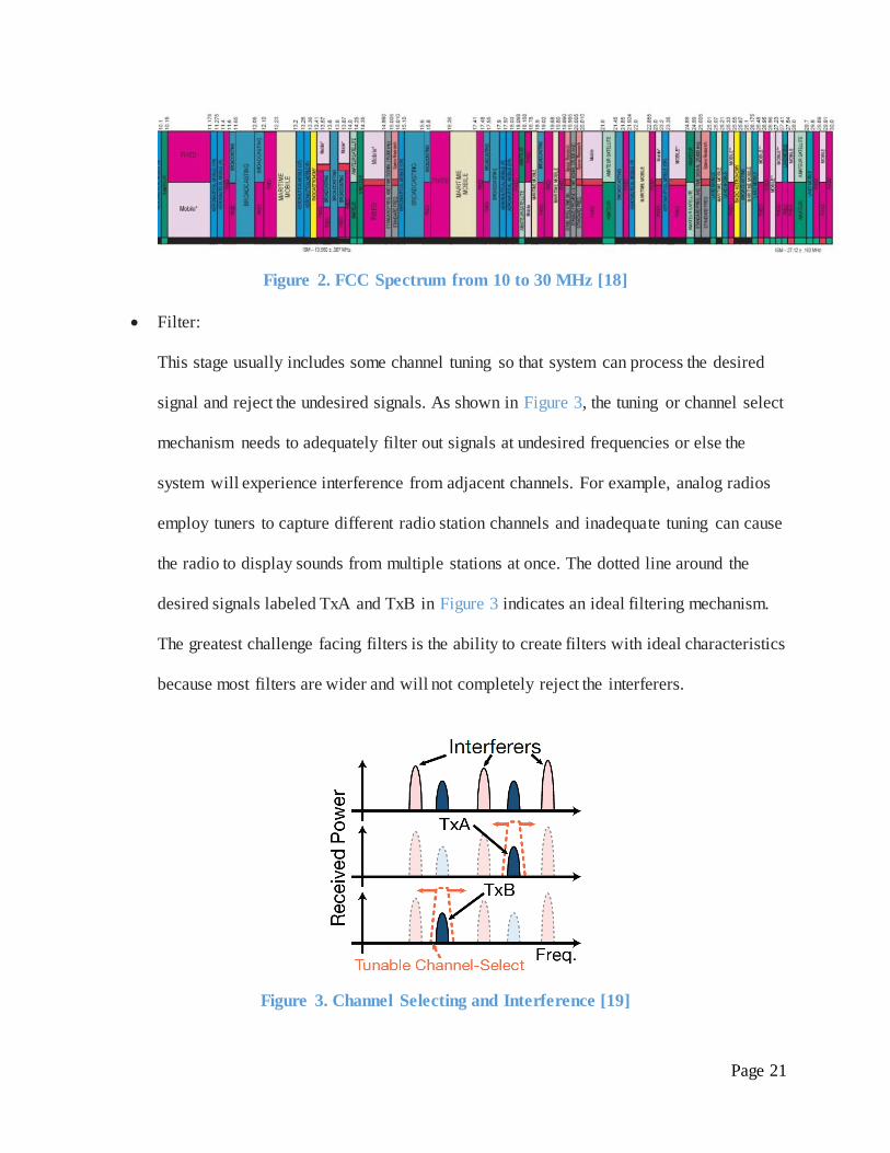
Figure 2. FCC Spectrum from 10 to 30 MHz [18]
Filter:
This stage usually includes some channel tuning so that system can process the desired
signal and reject the undesired signals. As shown in Figure 3, the tuning or channel select
mechanism needs to adequately filter out signals at undesired frequencies or else the
system will experience interference from adjacent channels. For example, analog radios
employ tuners to capture different radio station channels and inadequate tuning can cause
the radio to display sounds from multiple stations at once. The dotted line around the
desired signals labeled TxA and TxB in Figure 3 indicates an ideal filtering mechanism.
The greatest challenge facing filters is the ability to create filters with ideal characteristics
because most filters are wider and will not completely reject the interferers.
Figure 3. Channel Selecting and Interference [19]

Page 22
Demodulator:
Once the signal has reached this stage, it is processed with a demodulator to extract the
useful information, and depending on the modulation scheme employed, different
demodulators are used at this stage. For example, amplitude modulation (AM) stores the
information in the amplitude of a signal and frequency modulation (FM) stores the
information in the frequency. In the case of AM radio where the information is stored in
the amplitude, a simple demodulator could be a device that measures the amplitude of the
signal over time. In frequency domain, an AM detector can be achieved with a band pass
or low pass filter that captures the peaks, or low frequency content, of the signal.
Figure 4. AM Detector [20]
Our MEMS based wireless transceiver allows us to differ from many of the existing and
proposed technologies by eliminating the need for many of the power hungry building blocks
used in traditional architectures. This reduction in the overhead power requirement, paired with
the low power MEMS resonator device, has allowed for the creation of a system that consumes

Page 23
115 microwatts of power. Systems like the one proposed in [21] are designed to consume 1.8mW
of power, which is about 15 times less efficient than our system. Our capstone project is
advancing the field of radio frequency circuit design by opening the door for low power
applications, longer lasting devices, and more robust systems.
The schematic shown in Figure 5 demonstrates the system level concept of the MEMS based
transceiver proposed by our mentors Professor Clark Nguyen, Dr. Tristan Rocheleau and Thura
Lin Naing. The simplicity of the design allows us to eliminate the need for blocks such as the
LNA, mixer, and filter. Our capstone project built upon the concept proposed by our advisors by
adding several key blocks and by physically implementing the design. The blocks that this team
designed include an oscillator, an envelope detector, a comparator, a buffer and a power
amplifier.
Figure 5. MEMS Transceiver [19]
The MEMS (microelectromechanical system) resonator, is the first stage of the transceiver. The
remaining design of the transceiver required various electronic transistor circuits created in
180nm complimentary mosfet (CMOS) technology. The individual building blocks of the
transceiver serve the following purposes:

Page 24
MEMS Resonator:
The MEMS resonator is a high Q factor device that allows for highly selective tuning and
filtering. In this application, the Q factor describes the degree of selectivity and unlike the
typical architectures and filters shown in Figure 1, the filtering from the MEMS device
eliminates interfering signals with extremely high attenuation. In addition, the tunable
nature of the MEMS resonator means we can select many different channels or
frequencies and because of this, the system can be designed to support multiple
standards.
Oscillator:
The oscillator, much like the local oscillator seen in traditional architectures, serves as a
reference carrier signal. The oscillator is designed to feedback the signal to the MEMS
device to generate sustainable oscillations. Because the system employs frequency shift
keying (FSK) as the modulation scheme, the information is stored in the frequency of the
signal that is generated by the oscillator. In the case of this design, the oscillator operates
at 60MHz and the resonator converts the frequency information into amplitude
information via growing oscillation amplitudes.
Envelope Detector:
The output of the oscillator is fed into an envelope detector to extract the information
stored in the growing oscillations. Similar to Figure 4, the envelope detector measures of
the peaks of the oscillations to extract the stored binary information.
Comparator:
The binary information (1 or 0) is then decoded from the envelope detector’s peak
amplitude information by using a comparator and a threshold level. If the amplitude from

Page 25
the output of the envelope detector is above the threshold, the data is triggered to be a 1,
and if the amplitude is below the threshold, the data is triggered to be a 0. With this
comparing mechanism, our transceiver can successfully recover the desired waveform
consisting of 1’s and 0’s.
Buffer:
A buffer circuit is added to the system to allow for probing and debugging after the
fabrication process.
Power Amplifier:
In transmitting data, a power amplifier is needed to convert the input signal into a
significant amount of radio power that is suitable for transmission of the wireless
signal[24].
The envelope detector that I designed built upon existing bodies of work. In the methods and
materials section of this report, I highlight many of the challenges facing existing envelope
detector architectures that can be found in publications and technical reports.
Methods and Materials
In designing the envelope detector for the system shown in Figure 5, I kept in mind the intended
application of the transceiver. First and foremost, the envelope detector needed to be extremely
low power because the entire system had to consume about 115 microwatts of power and the
majority of the power budget was allocated for the power amplifier and oscillator. Therefore, the
final design of my envelope detector needed to operate on nanowatts of power. Second, the
envelope detector needed to be able to measure amplitude variations as small as several

Page 26
microvolts. Third, the detector needed to be able to demodulate very low amplitude signals that
are close to the noise floor. Fourth, the envelope detector could not introduce too much
additional noise into the system. Lastly, the envelope detector needed to be temperature
independent because any variation to the bias level of the circuit will affect the threshold level of
Keli’s comparator. All of these specifications turned what would’ve been a simple design into a
complicated circuit. The method and approach I took in accomplishing my goal of designing a
circuit meeting the above specifications included a thorough review of known circuit topologies.
Classic envelope detectors are simple to design because they require a basic diode and low pass
filter circuit. However, to meet the specifications laid out above, the envelope detector I designed
needed to be based off an entirely different architecture. The main issue with using the classic
diode detector with low pass filter circuit configuration is highlighted in a technical report
published by Professor Jan Rabaey and Postdocal Researcher Simone Gambini of UC Berkeley
[25]. According to the report, a significant amount of gain needs to be applied to the radio
frequency signal prior to entering the envelope detector because the signal can pass through the
detector only if the amplitude is above the diode semiconductor turn-on voltage. In other words,
if the amplitude is not high enough, the signal will not pass through the detector and will not be
demodulated properly. In our low power application, the amplitude of the input signal is
estimated to be in the millivolt range which is far below the required minimum .7V turn-on
voltage of nominal discrete diodes. A solution to this problem would be to apply the necessary
gain to the signal prior to the envelope detector, but this would mean higher power consumption.
In an effort to find a suitable low power solution to resolve this problem, I attempted topologies
found in various publications. In an Institute of Electrical and Electronic Engineers (IEEE)
publication by researchers from Seoul National University, an operational transconductance
Page 27
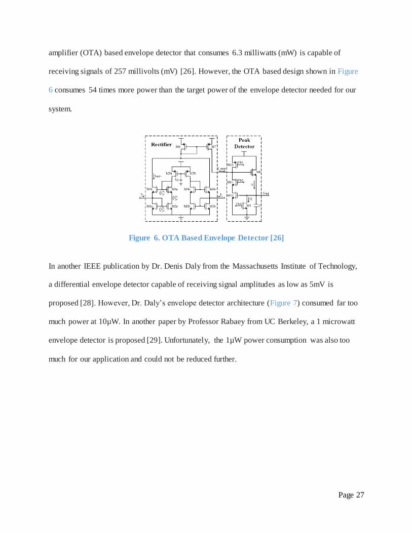
amplifier (OTA) based envelope detector that consumes 6.3 milliwatts (mW) is capable of
receiving signals of 257 millivolts (mV) [26]. However, the OTA based design shown in Figure
6 consumes 54 times more power than the target power of the envelope detector needed for our
system.
Figure 6. OTA Based Envelope Detector [26]
In another IEEE publication by Dr. Denis Daly from the Massachusetts Institute of Technology,
a differential envelope detector capable of receiving signal amplitudes as low as 5mV is
proposed [28]. However, Dr. Daly’s envelope detector architecture (Figure 7) consumed far too
much power at 10µW. In another paper by Professor Rabaey from UC Berkeley, a 1 microwatt
envelope detector is proposed [29]. Unfortunately, the 1µW power consumption was also too
much for our application and could not be reduced further.

Page 28
Figure 7. Differential Envelope Detector [28]
Finally, I settled for a source follower circuit with a peak detection capacitor at the output. The
motivation for this design came from a publication by Professor Robert Meyer from UC
Berkeley [27]. The design proposed by Robert Meyer, shown in Figure 8, was based off of
bipolar junction transistors and consumed 20-50 microwatts of power.
Figure 8. BJT Envelope Detector [27]
I built upon the design shown in Figure 8 by implementing the topology in 180nm CMOS
transistors. I also converted the design into a single ended implementation, added a PMOS in
triode for high frequency rejection, and successfully lowered the power consumption to 167.1
nanowatts (nW). I also added a copy of the input branch that is used to supply the bias voltage as
a reference voltage for the comparator. The envelope detector I designed is shown in Figure 9
and is capable of recovering signals with amplitudes as low as 2mVpp, which is an improvement
on the higher power designs proposed by researchers at other universities. Through simulations

Page 29
in Cadence and the ADE tool suite, I was able to confirm the operation of the envelope detector.
Those simulation results can be found in the next section of this report.
Figure 9. Single Ended Source Follower Envelope Detector
After successfully creating a low power envelope detector suitable for our transceiver system, the
next daunting task was designing a current reference capable of supplying 83 nanoamps (nA) of
current. Because the circuit operated at such low power, I needed to design a very stable current
reference to supply the extremely low current needed to bias the envelope detector. I began my
design by referring to a circuit proposed by Keith Sanborn from the University of Arizona [31].
In his paper, Dr. Sanborn proposed a folded cascade with temperature dependence cancellation
bandgap reference design that supplies 20 microamps (µA) of current. Following Dr. Sanborn’s
example, I designed my current reference using the same method of generating a stable and
temperature independent circuit.
The final design of my current reference is shown in Figure 10 and is capable of supplying 83nA
of current with a negligible .3% variation across the 0°C to 70°C temperature range. This

Page 30
stability was achieved by cancelling the temperature dependence of the resistor in the circuit with
a diode connected NMOS transistor in parallel. The low current supply was achieved using
maximum long channel devices in 180nm TSMC transistors. The main issue that rises when
operating at low currents is noise and this problem is further exacerbated because the current
source directly biases the envelope detector. Therefore, the noise produced by the current source
will degrade the input signal due to the unity gain source follower topology of the envelope
detector [30]. An extensive noise analysis was conducted by hand and verified with simulation
on Cadence. The results indicate that the noise generated by this low current reference is
-142.5dBm at the 60MHz operating frequency.
Figure 10. Temperature Independent Current Reference
With the design of the low power envelope detector and low current reference circuit complete,
the building block is ready to be implemented into a working transceiver system. In the next
sections, I will highlight the performance of the standalone envelope detector with current
reference. I will also discuss the results of the system level integration with Han’s oscillator and
Keli’s comparator to form the front end receiver.

Page 31
Technical Contributions
The final design of the envelope detector with current reference is shown in Figure 11.
Figure 11. Envelope Detector and Current Reference
From the noise simulation discussed previously, the noise floor of the overall block is found to
be -142.5dBm at the 60MHz operating frequency. The noise equivalent circuit used for the hand
calculations is shown in Figure 12. The noise simulation plots verifying the hand calculation is
shown in Figure 13. From the equation below, the minimum detectable signal with a nominal
noise figure (NF) and signal-to-noise ratio (SNR) requirement is
Min Det. Signal = Noise Floor + 10log(BW) + NF + SNR
Min Det. Signal = -53.9dBm

Page 32
Figure 12. Noise Equivalent Circuit
Figure 13. Noise Plot
Therefore, this envelope detector is capable of demodulating radio frequency signals with
amplitudes as low as 2mVpp before the signal is overrun with noise. The simulation proving the
ability to demodulate signals with 2mVpp amplitude is shown in Figure 14. On the other end of
the spectrum, the maximum amplitude the envelope detector can detect before clipping is
simulated to be 1V. Therefore, the dynamic range of this block is
0𝑑𝐵𝑚− (−53.9𝑑𝐵𝑀) = 53.9𝑑𝐵.

Page 33
Figure 14. Minimum Detectable Signal
To reiterate, my goal for this particular building block was to design a low power envelope
detector capable of receiving low voltage radio signals. Additionally, the low power envelope
detector was to be biased with a stable low current reference. As shown in the simulation results,
I was successfully able to accomplish these goals and my final design operates on 83nA on a
1.8V supply for a total consumption of 250.6nW. The current reference has four branches and
with each branch drawing 83nA on a 1.8V supply, the total power consumption is 417.7nW. As
hoped, the current reference is temperature stable with a negligible .3% variation over the 0°C to
70°C temperature range, and the envelope detector is capable of receiving signals at amplitudes
as low as 2mVpp.
After successfully designing the crucial envelope detector block, the capstone team set forth with
integrating all the blocks into a functional transceiver system. The results of that integration will
be discussed in the final summary. We encountered many problems when implementing the
entire system because we could not simply piece the individual building blocks together. We

Page 34
discovered that some slight modifications needed to be performed before the system functioned
properly.
As part of the integration process, I also designed the layout of the envelope detector schematic
and the oscillator. The results of the layout is shown in Figure 15 and final area for this layout is
750um^2.
Figure 15. Layout of Oscillator and Envelope Detector
Page 35
SYSTEM SUMMARY
This chapter of the report will provide the summary of the system level integration and
performance of the receiver and transmitter. This chapter will provide a summary of the
oscillator, comparator, power amplifier, and buffer blocks. For cohesiveness, this chapter will
also include an abridged version of my technical contributions in the envelope detector.
Oscillator
The function of oscillator in a transceiver system is to create a constant high frequency signal to
carry the information signal. In a transmitter system, the oscillator output modulates the
information signal, and the power amplifier amplifies the signal to be transmitted afterwards. In
the receiver chain, the oscillator and envelope detector demodulates the transmitted signal and
then sends it to comparator for decoding.
The oscillator in this system is designed as a MEMS-Based oscillator, where the MEMS device
is used as a resonator to replace the crystal that is used in traditional oscillators. The advantage of
the MEMS-Based oscillator is that it provides high Q to have a more accurate channel selection,
and the simple design also contributes to low power consumption.
Oscillators typically consume the majority of power in the receive chain. Therefore, the topology
of the oscillator determines the power consumption of whole system at some degree. Based on
the low power consumption specification, the Pierce oscillator schematic, which consumes
relatively low power, is being used. The schematic is shown below in Figure 16:

Page 36
Figure 16: Pierce Oscillator
The feedback loop of this oscillator has a phase shift of 360°, and in order to make it oscillate,
we also need to design for a negative resistance greater than 8.5kΩ looking into two ports of
resonator. Since positive resistance consumes power, we can regard negative resistance as an
energy source. If this “energy source” provides energy larger than the power consumption of
resistor in the resonator, then this oscillator can work well.
According to the equation of negative resistance:
Re(Zc ) = -gmC1C2
(gmC3)2 +w2(C1C2 +C2C3 +C3C1)
2
In the circuit shown in Figure 16, the nodes “IN” and “OUT” link with the MEMS device by
bond pad connection, and we assume the parasitic capacitance on the bond pad is around 250fF.
The transconductance of the common source amplifier is 165.68uA/V, and the value of negative
resistance is 13.66kΩ.
The output waveform and power consumption is shown below in Figure 17 and Figure 18.

Page 37
Figure 17: Growing Waveform Of The Oscillator
Figure 18: Power Consumption Of The Oscillator
The resonance frequency of 58.98MHz, and the amplitude is 128mV. The power consumption is
15uW.
The amplitude of the oscillator output in each period differentiates ‘1’ and ‘0’. The simulation
required different stimulating signals to generate the different growing speed. Further, the

Page 38
oscillator required a reset to toggle a ‘0’ in simulation. The reset to the oscillator was generated
by switching the resonator resistance to a much higher resistance to destroy the quality factor.
The stimulating circuit with a reset is shown in Figure 19.
Figure 19. Stimulating Circuit
R1 corresponds to the working state, and R2 corresponds to resetting state. When the circuit
switches to R2, the high resistance destroys the quality factor so that the oscillator can no longer
work. The switch S1 is set to be periodically switches between R1 and R2. The output waveform
is shown below in Figure 20.
Figure 20. Output Waveform of Oscillator
In addition, an FSK signal is needed on the transmitter side. The method to generate an FSK
signal is to switch the value of capacitance between two values. 7aF capacitance was used to
Page 39
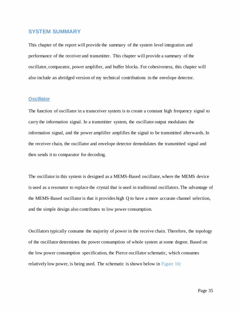
generate 59MHz signal, and 6.5aF capacitance to generate 61MHz signal. The MEMS resonator
model is shown below in Figure 21:
Figure 21. MEMS Resonator Model
Design Specification Value
Resonance frequency 58.9MHz
Power Consumption 15uW
Envelope Detector
The envelope detector designed is a key piece of the transceiver system because it serves to
detect the information stored in the envelope of wireless signals. In order to bias the envelope
detector circuit into a temperature stable state of operation, a temperature independent current
source was implemented. This temperature independent current source was also taken advantage
of by the oscillator and the buffer circuits.
The design of the envelope detector had several key specifications. The consumption of the
envelope detector was limited to several nW. Second, the envelope detector needed to be able to
measure amplitude variations as small as several microvolts with good carrier rejection. Lastly,
the envelope detector needed to be temperature independent because any variation to the bias
level of the circuit will affect the threshold level of Keli’s comparator.

Page 40
Classic envelope detectors are simple to design because they require a basic diode and low pass
filter circuit. However, to meet the specifications laid out above, the envelope detector used in
this system needed to be based off an entirely different architecture. The main issue with using
the classic diode detector with low pass filter circuit configuration, as highlighted in [25], is the
need for a significant amount of gain to bring the radio frequency amplitude above the turn on
voltage of the diode. The high gain required in the classic diode detector is not suitable for our
low power design. Many of the alternative envelope detector architectures capable of receiving
low radio signals consumed far too much power. In [26], an operational transconductance
amplifier (OTA) based envelope detector can demodulate signals as low as 257mV while
consuming 6.3mW of power. In [27], [28] and [29], differential envelope detectors capable of
receiving RF as low as 5mV consumed 20µW, 10µW and 1µW respectively.
The envelope detector implemented in this transceiver was designed with 180nm TSMC process.
The design implemented a single ended source follower stage with low bandwidth to filter out
the carrier. A PMOS biased in the triode region is used in the output stage for capacitive low
pass filtering. A copy of the input branch is also used to supply the DC bias voltage as a
reference voltage for the comparator. The final envelope detector, shown in Figure 22, is capable
of recovering signals with amplitudes as low as 2mVpp. Overall, the envelope detector
consumed 167.1nW of power.

Page 41
Figure 22. Single Ended Source Follower Envelope Detector
The noise equivalent circuit used for the hand calculations is shown in Figure 23. The noise
simulation plots verifying the hand calculation is shown in Figure 24. From the equation below,
the minimum detectable signal with a nominal noise figure (NF) and signal-to-noise ratio (SNR)
requirement is
Min Det. Signal = Noise Floor + 10log(BW) + NF + SNR
Min Det. Signal = -53.9dBm
Figure 23. Noise Equivalent Circuit

Page 42
Figure 24. Noise Plot
Therefore, the minimum detectable is 2mVpp. The simulation proving the ability to demodulate
signals with 2mVpp amplitude is shown in Figure 25. On the other end of the spectrum, the
maximum amplitude the envelope detector can detect before clipping is simulated to be 1V.
Therefore, the dynamic range of this block is
0𝑑𝐵𝑚− (−53.9𝑑𝐵𝑀) = 53.9𝑑𝐵.
Figure 25. Minimum Detectable Signal

Page 43
The envelope detector discussed was biased with 83nA of current and required stable reference
supply. The design of the reference followed the methodology proposed in [30], which discusses
a stable bandgap reference. The final design of the current reference is shown in Figure 26 and is
capable of supplying 83nA of current with a 0.3% variation across the 0°C to 70°C temperature
range. This stability was achieved by cancelling the temperature dependence of the resistor in the
circuit with a diode connected NMOS transistor in parallel. The low current supply was achieved
using maximum long channel devices in 180nm TSMC transistors.
Figure 26. Temperature Independent Current Reference

Page 44
The final design of the envelope detector with current reference is shown in Figure 27.
Figure 27. Envelope Detector and Current Reference
As part of the integration process, the layout of the envelope detector, current reference and the
oscillator was designed. The layout is shown in Figure 28 with a die area of 750um^2.
Figure 28. Layout of Oscillator, Current Supply, and Envelope Detector
Page 45
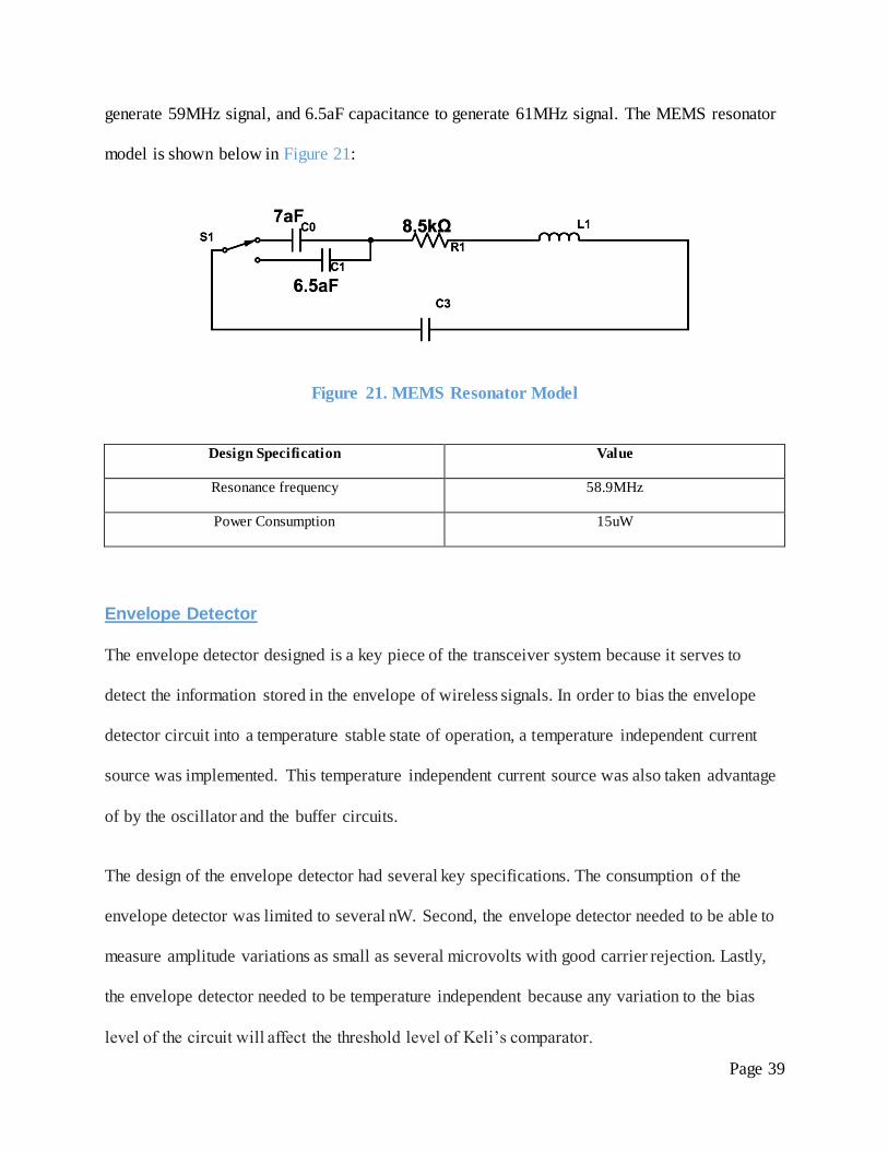
Block Summary
Envelope Detector
Minimum Detectable Signal 2mVpp
Dynamic Range 53.9dB
Envelope Delay .5us
Envelope Bandwidth 1MHz
Carrier Bandwidth 500MHz
Total Power Consumption 167.1nW
Current Reference
DC Current 0°C 83.21nA
DC Current 25°C 83.55nA
DC Current 70°C 83.89nA
Total Power Consumption 250.6nW
Layout
Die Size (Oscillator, Envelope Detector, Current Source) 750um^2

Page 46
Comparator
When Frequency Shift Keying (FSK) modulated signals enter the transceiver, they give rise to
the periodically restarted oscillations [1]. When the oscillation envelope is detected, the
comparator should be able to discriminate “0”s and “1”s [1].
The schematic for the comparator is shown below in Figure 29.
Figure 29. Comparator Schematic
The benefit of this design is that in the reset phase, when the clock signal is low, voltage supply
and ground are disconnected from the latch. Therefore, no power consumption occurs in this
phase. Since digital circuits normally only accept supply voltage and ground voltage as “1”s and
“0”s, a PMOS pair was added to pull the output to supply voltage. During the evaluation phase,

Page 47
when the clock signal is high, the comparator is powered and starts to compare the input signals
at the “In+” and “In-” terminals. The latch circuit grows the input difference and finally reflects
either “1” or “0” at the output terminal.
The functionality of the comparator is confirmed with Figure 30. The first plot is the input signal,
the second one is the clock signal and the third one is the output signal. The test signal was a
sinusoidal wave with 1mV amplitude at 800mV DC level. The reference voltage used to
discriminate the “0” and “1” was 800mV. From the output signal plot, it is shown that when the
clock is on, if the input signal is above 800mV, the output is “1”; vice versa.
Figure 30. Comparator Functionality
This comparator circuit consumes 237nW of power, which fits our team’s purpose of building an
ultra-low power transceiver.

Page 48
Complete Receiver Chain
The schematic for the complete receiver chain, which consists of the oscillator, the envelope
detector, and the comparator, is shown in Figure 31.
Figure 31. Receiver Chain
The capstone team verified the functionality of the receiver chain by inputting a test 1010 signal
that is generated by the oscillator. The results of the simulation are shown in Figure 32. As
shown, the green signal is the generated 1010 signal from the oscillator. The purple square wave
is the output of the envelope detector and as expected, it is the negative envelope of the input
oscillator signal. The dc purple signal represents the reference voltage that the comparator uses
to determine the received bits. For envelope amplitudes below the reference level, the
comparator will clock a 1 and for envelope amplitudes above the reference level, the comparator
will clock a 0. The red signal represents the clock signal. The blue signal represents the output of
the comparator. An output synchronous flip flop that is edge triggered by the clock shown will
latch a 1010, as expected.

Page 49
Figure 32. Verification of Receiver
Power Amplifier
This part of the paper summarizes the design of a Power amplifier (PA) for the transmitter part
of the system. This block functions to establish connections and send information from the
digital system to the external world.
Given the fact that reducing the power consumption is the overall goal of this project, the power
consumed by the individual blocks must also be minimized. This translates to the concept of
power efficiency, meaning ‘the amount of power used to generate and transmit a decodable burst
of data from the system’. The major trade off for efficiency is a characteristic called linearity.
Linearity defines ‘the relationship between the output and the input, and the change in output for
Page 50
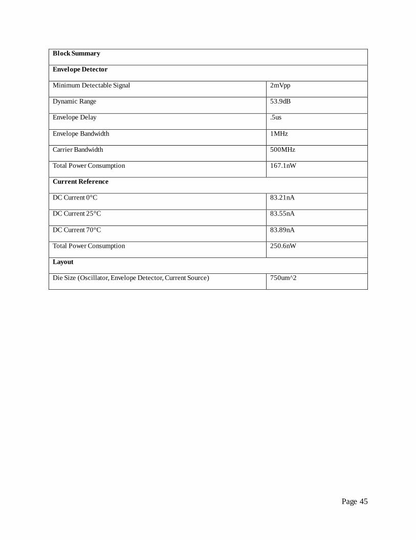
a given change in the input level’. Below is a table of the performance statistics of each of the
power amplifier classes available.
CLASS A B C D E
Theoretical efficiency 50% 78.5% 80% 100% 100%
Linearity Linear Non-linear Non-linear Non-linear Non-linear
Since efficiency is our major consideration in this system, a class D amplifier was used. This
choice was made after surveying highly efficient PA’s in papers written in [32] and [33]. The
other requirements needed for proper operation of the PA block include current bias generation,
voltage bias at the input, and inclusion of passives.
Figure 33. Class D & E Amplifier models [34]
From the above table, class D and class E amplifiers can be theoretically characterized as having
an efficiency of 100% [34], this is because they don’t allow for any dissipation of energy within
the system, thus translating all of its energy to the required output load, which is an antenna used
for transmission in most cases.

Page 51
Figure 34. Architecture of the Power Amplifier
The control over power transmitted to the load depends on the impedance (resistance) of the load
seen by the output node of the amplifier. In order to meet the specification of the power drawn
by the load precisely, this load seen by the output node has to be transformed to a different value.
This process of transforming the load can be done by using a network called ‘matching network’
to match the output node to the impedance needed for maximum power transfer. For this power
amplifier, a T-match was employed because it isolates the DC component and the AC
component – which is of our interest at the output node and also provides the impedance
transformation needed. The final schematic of the power amplifier is shown in Figure 35.
Figure 35. Power Amplifier Schematic
The layout of the power amplifier is shown in Figure 36.

Page 52
Figure 36. Power Amplifier Layout
The reported power gain is 47 dB at the fundamental frequency. The reported efficiency is
86.35% as shown in Figure 37.
Figure 37. Measured Power Gain & Efficiency

Page 53
Transmit Chain
The oscillator is integrated with the Power amplifier by connecting the output of the oscillator to
the input of the PA. An input FSK is generated by the oscillator and given to the PA.
The plot below shows how an input data stream is modulated and transmitted by the power
amplifier into the antenna.
Figure 38. Transmit Waveform

Page 54
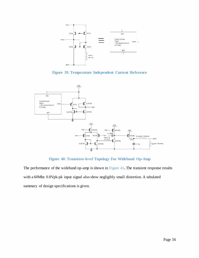
Voltage Buffer
The design requires a voltage buffer to interface with the 50Ω transmission line required to test
our chip. This voltage buffer has several design requirements. The most important is a voltage
gain of 1 to accurately represent the input signal. Impedance matching at the output is necessary
to ensure that the maximum available power from the input signal is delivered to the load. The
buffer also requires high enough bandwidth, output voltage swing, and linearity to send signals
to the output negligible distortion. The input signals of interest are a 60MHz signal centered at
600mV with 0.8V peak to peak (pk-pk) and a 5kHz signal with 1.8Vpk-pk. A bandwidth
requirement of 600MHz is necessary to capture harmonics of the 60MHz signal. Additionally,
the buffer will connect a separate power rail from the rest of the transceiver to negate its power
contribution during normal operation of the MEMS transceiver.
Given the design requirements presented, two separate buffers were implemented. A wideband
buffer was designed for the 60MHz signal, while a rail-to-rail buffer was designed for the 5khz
signal. There exist a variety of different approaches to implement voltage buffers. Many single-
stage amplifiers are described in the literature [35] [36] [37] [38]. These topologies are desired
over op-amp based approaches mainly for their design simplicity and potential savings in die
area and power consumption. However, their main disadvantage is the inability to reach the
theoretical voltage gain of 1. Therefore, these topologies were not considered.
A different approach relies on tying an op amp into unity-gain feedback to set the voltage gain to
1. This feedback also decreases the output resistance by approximately the open-loop gain of the
op amp, which further favors the conditions of an ideal voltage buffer. To properly send the large

Page 55
input signals for our application, the op amp needs to have a large enough input common mode
and output voltage swing. The op amp must also have the capability to drive low impedances,
which requires the implementation of an output stage. For temperature independence, we also
require a temperature independent current reference. The design of this reference is taken from
[39] and is shown in Figure 39.
The design of the wideband op-amp for the 60Mhz signal is shown in Figure 40. The three stage
op-amp topology consists of an input differential stage followed by a gain stage and an output
stage. A series resistor and capacitor are used to increase stability in unity-gain feedback by
moving the right half plane zero on top of the second pole. The output stage consists of a
common source PMOS transistor, allowing the output to swing up to Vdd-Vov. By contrast, if a
source follower was used, the output could only swing up to Vdd-(Vgs+Vov). Since our 60Mhz
signal needs to swing up to 1V and Vgs+Vov > 800mV, the source follower output stage would
not have suited our application. The output stage resembles a push-pull inverter, but only the
PMOS half is needed since we do not swing below 0V.
The output of our op amp in Figure 40 shows the approach that is taken toward the impedance
matching problem. The weakness of our unity gain feedback configuration is that the output
resistance is not a clearly defined value. We can remedy this by adding an off-chip 50Ω resistor
in series to have a matching impedance of about 50Ω, assuming that the op amp tied in feedback
has a very low impedance. This systematically reduces the voltage gain by ½, which is not
detrimental since we can take this into account when viewing the waveform.
Page 56
Figure 39. Temperature Independent Current Reference
Figure 40. Transistor-level Topology For Wideband Op-Amp
The performance of the wideband op-amp is shown in Figure 41. The transient response results
with a 60Mhz 0.8Vpk-pk input signal also show negligibly small distortion. A tabulated
summary of design specifications is given.

Page 57
Figure 41. Wideband Op Amp Connected In Unity-gain Feedback
Design Spec Wideband op-amp
DC Gain 1.0
3dB Bandwidth 1.9Ghz
1dB Av compression point (input signal DC level 600mV)
0.9V (Vpk-pk)
Total Power Consumption 12.4mW
Temperature Variations with Idc +- 5%
Output Impedance 50.44Ω at 60Mhz
Phase Margin 60.4 degrees
Frequency where loop gain is 0dB 1Ghz
The design of the rail-to-rail op-amp for the 5khz signal is shown in Figure 42 and replicates a
design presented in [40]. An op-amp that can handle a rail-to-rail signal requires an input stage
with a rail-to-rail common mode input range and an output stage with a rail-to-rail output swing.
The input stage is a complementary differential pair with a cascoded load (Comp-Casc); it is
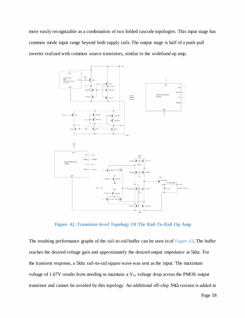
Page 58
more easily recognizable as a combination of two folded cascode topologies. This input stage has
common mode input range beyond both supply rails. The output stage is half of a push-pull
inverter realized with common source transistors, similar to the wideband op amp.
Figure 42. Transistor-level Topology Of The Rail-To-Rail Op Amp
The resulting performance graphs of the rail-to-rail buffer can be seen in of Figure 43. The buffer
reaches the desired voltage gain and approximately the desired output impedance at 5khz. For
the transient response, a 5khz rail-to-rail square wave was sent as the input. The maximum
voltage of 1.67V results from needing to maintain a Vov voltage drop across the PMOS output
transistor and cannot be avoided by this topology. An additional off-chip 50Ω resistor is added at
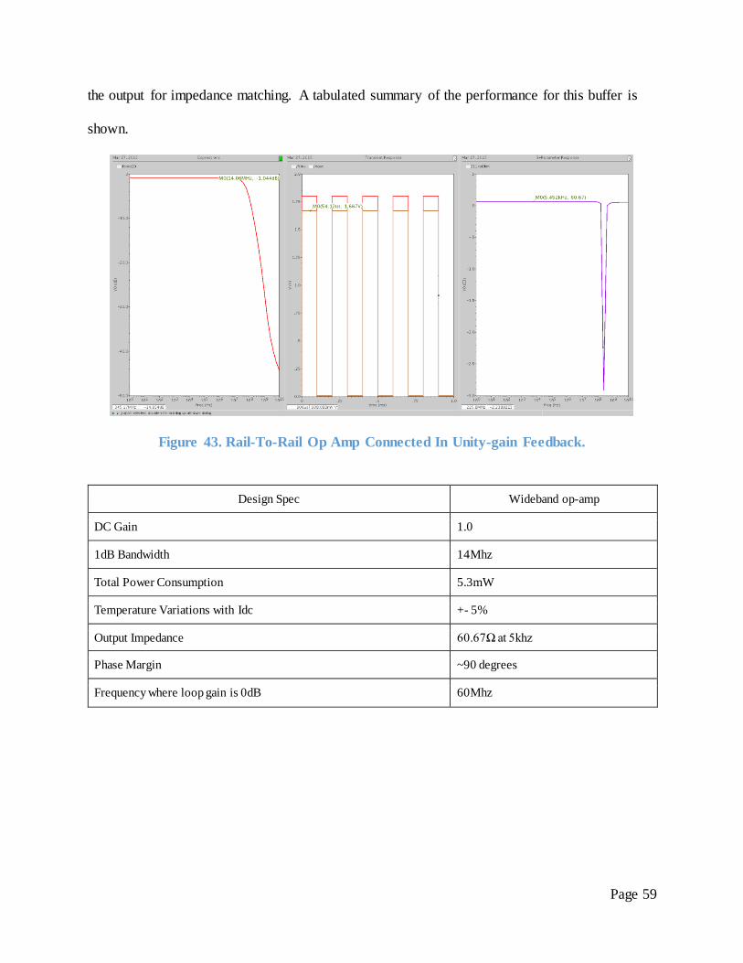
Page 59
the output for impedance matching. A tabulated summary of the performance for this buffer is
shown.
Figure 43. Rail-To-Rail Op Amp Connected In Unity-gain Feedback.
Design Spec Wideband op-amp
DC Gain 1.0
1dB Bandwidth 14Mhz
Total Power Consumption 5.3mW
Temperature Variations with Idc +- 5%
Output Impedance 60.67Ω at 5khz
Phase Margin ~90 degrees
Frequency where loop gain is 0dB 60Mhz

Page 60
CONCLUSION
Our final prototype was designed using 180nm CMOS technology on Cadence, and the
schematic was generated as part of this project. With the schematic of the system and layout of
the oscillator/envelope detector complete, this transceiver system is almost ready for fabrication.
However, the fabrication process usually takes several months and thus, this capstone team does
not anticipate the opportunity of verifying the physical circuit. Despite this, we are confident in
our simulation results and believe that the transceiver system designed in this project is
functional and ready for applications.
The outcome discussed in this report reveals that it is possible to create a low power MEMS
based transceiver. We successfully achieved our goal of designing a system that operates on 115
microwatts of power. In our market analysis, this capstone team identified many different
applications for our technology and found that there is an immense need for low power
transceiver systems in markets such as home, health, and agriculture. By successfully fulfilling
our goals laid out in this capstone project, we have proven our hypothesis and we are excited to
see where this technology is headed.

Page 61
WORKS CITED
[1] Rocheleau, T., Naing, T., Nilchi, J., & Nguyen, C. (2014). A MEMS-BASED TUNABLE RF
CHANNEL-SELECTING SUPER-REGENERATIVE TRANSCEIVER FOR WIRELESS
SENSOR NODES.Tech. Digest, 83-86.
[2] Nguyen, C. (2013, April 1). MEMS-Based RF Channel Selection for True Software-Defined
Cognitive Radio and Low-Power Sensor Communications. IEEE Communications Magazine,
110-119.
[3] Smith, P. (2011). Comparing Low-Power Wireless Technologies. Retrieved November 25,
2014. http://www.digikey.com/en/articles/techzone/2011/aug/comparing-low-power- wireless-
technologies.
[4] Dye, N., & Granberg, H. (2001). Radio frequency transistors principles and practical
applications (2nd ed., p. 32). Boston: Newnes.
[5] Lawson, S. (2014, November 18). ZigBee 3.0 promises one smart home standard for many
uses. PCWorld.
http://www.pcworld.com/article/2849172/zigbee-30-promises-one-standard-for-many-uses.html
[6] Siekkinen, M., Hiienkari, M., & Nurminen, J. (2012). How Low Energy is Bluetooth Low
Energy? Comparative Measurements with ZigBee/802.15.4. Embracing Machine-to-Machine
Communications and Beyond, 232-237. Retrieved from
http://www.eecs.umich.edu/courses/eecs589/papers/06215496.pdf
[7] Peiris, V. (2013). Highly integrated wireless sensing for body area network applications.
SPIE,1-3.
[8] Hart, J., & Martinez, K. (2006, July 7). Environmental Sensor Networks: A revolution in the
earth systems science? Earth-Science Reviews, 177-190.
[9] Porter, M. (2008). The Five Competitive Forces that Shape Strategy. Harvard Business
Review, 86-104, 431-452.
[10] Sensors Value Chain. (2012). Retrieved February 13, 2015, from http://gtq.imb-
cnm.csic.es/en/about-us/sensors-value-chain
[11] Ulama, Darryle. (2014, December). IBISWorld Industry Report 33441a: Semiconductor and
Circuit Manufacturing in the US. Retrieved February 13, 2015, from
http://clients1.ibisworld.com/reports/us/industry/default.aspx?indid=752
[12] Neville, A. (2014). IBISWorld Industry Report OD4422 Precision Agriculture Systems &
Services. 3-26. Retrieved February 14, 2015, from www.ibis.com
Page 62
[13] Gerson, D. (2014, December 1). Smarter Food. Retrieved February 1, 2015, from
http://www.ibm.com/smarterplanet/us/en/food_technology/article/food_technology.html
[14] Gainer, K. (2009). Environmental Sensing and Monitoring Technologies: Global Markets.
(IAS030A), 1-1. Retrieved February 13, 2015, from http://www.bccresearch.com/market-
research/instrumentation-and-sensors/environmental-sensing-monitoring-ias030a.html
[15] American Farm Bureau Federation(2014). Fast fact about agriculture. Accessed February
14, 2015. from http://www.fb.org/index.php?fuseaction=newsroom.fastfacts
[16] Southwire 2015 Distributor List Price Sheet: Copper Building Wire.
http://www.southwire.com/documents/pricesheets/466C.pdf, accessed February 11, 2015.
[17] Frenzel, Loue. "SDR And CR Boost Wireless Communications." SDR And CR Boost
Wireless Communications. Electronic Design, 12 Oct. 2011. Web. 10 Mar. 2015.
<http://electronicdesign.com/dsps/sdr-and-cr-boost-wireless-communications>.
[18] Ismail, Sherille. "Transformative Choices: A Review of 70 Years of FCC
Decisions." Journal of Information Policy 1 (2011): 6-35. Federal Communications Commission,
25 July 2014. Web.
[19] Rocheleau, Tristan. "“A MEMS-based Tunable RF Channel-selecting Super-regenerative
Transceiver for Wireless Sensor Nodes." Solid-State Sensors, Actuators and Microsystems
Workshop (2014): n. pag. Web.
[20] Lesurf, Jim. "The Envelope Detector." The Envelope Detector. University of St. Andrews,
n.d. Web. 10 Mar. 2015. <https://www.st-
andrews.ac.uk/~www_pa/Scots_Guide/RadCom/part9/page2.html>.
[21] Cha, Jeongwon. "A CMOS Radio-frequency Front-end for Multi-standard Wireless
Communications." A CMOS Radio-frequency Front-end for Multi-standard Wireless
Communications. Georgia Institute of Technology, 3 Mar. 2011. Web. 10 Mar. 2015.
<https://smartech.gatech.edu/handle/1853/37250?show=full>.
[22] Xia, Lingli. "Chapter 6." Ultra Wideband RF Transceiver Design in CMOS Technology.
Intech, 2011. Web. 10 Mar. 2015. <http://www.intechopen.com/books/ultra-wideband-
communications-novel-trends-system-architecture-and-implementation/ultra-wideband-rf-
transceiver-design-in-cmos-technology>.
[23] Lai, Xiongliang. "A Comparative Study of Low-power CMOS Gilbert Mixers in Weak and
Strong Inversion." IEEE Xplore. Institute of Electrical and Electronic Engineers, 7 Aug. 2011.
Web. 10 Mar. 2015.
[24] Raab, F.h., P. Asbeck, S. Cripps, P.b. Kenington, Z.b. Popovic, N. Pothecary, J.f. Sevic, and
N.o. Sokal. "Power Amplifiers and Transmitters for RF and Microwave." IEEE Transactions on
Microwave Theory and Techniques 50.3 (2002): 814-26. Web.

Page 63
[25] Gambini, Simone. "Sensitivity Analysis for AM Detectors." Sensitivity Analysis for AM
Detectors. UC Berkeley, 6 Apr. 2008. Web. 10 Mar. 2015.
<http://www.eecs.berkeley.edu/Pubs/TechRpts/2008/EECS-2008-31.html>.
[26] Zhou, Yanping. "A Novel Wide-band Envelope Detector." IEEE Xplore. N.p., 17 June
2008. Web. 10 Mar. 2015.
<http://ieeexplore.ieee.org/xpl/articleDetails.jsp?arnumber=4561422>.
[27] R.G. Meyer Low-power monolithic RF peak detector analysis IEEE Journal of Solid-State
Circuits, January 1995.
[28] D.C.Daly and A.Chandrakasan An energy efficient OOK transceiver for wireless sensor
networks IEEE Journal of Solid-state Circuits, May 2007.
[29] Pletcher, Nathan, Jan Rabaey, and Simone Gambini. "A 65uW, 1.9 GHz RF to Digital
Baseband Wakeup Receiver for Wireless Sensor Nodes." IEEE Xplore. N.p., 16 Sept. 2007.
Web. 10 Mar. 2015. <http://ieeexplore.ieee.org/xpls/abs_all.jsp?arnumber=4405789>.
[30] Alon, Elad. "EE240: Advanced Analog Integrated Circuits Lectures." EE240 (Spring 2009).
N.p., 2009. Web. 10 Mar. 2015.
<http://bwrcs.eecs.berkeley.edu/Classes/icdesign/ee240_sp10/lectures.html>.
[31] Sanborn, Keith. "A Sub-1-V Low-Noise Bandgap Voltage Reference." IEEE Xplore. N.p.,
Nov. 2007. Web. 10 Mar. 2015.
<http://ieeexplore.ieee.org/stamp/stamp.jsp?arnumber=4362111>.
[32] Nathan o. sokal,(1981) ieee life fellow design automation, inc: Class-e high-efficiency
rf/microwave power amplifiers: principles of operation, design procedures, and experimental
verification retrieved Feburary 1981 from:
http://www.cs.berkeley.edu/~culler/AIIT/papers/radio/Sokal%20AACD5-poweramps.pdf
[33] N.O.Sokal and A.D.Sokal (1975),“Class E—A new class of high-efficiency tuned single-
ended switching power amplifiers,” IEEE J. Solid-State Circuits, vol. SC-10, no. 6, pp. 168–176,
Jun. 1975. http://ieeexplore.ieee.org/xpls/abs_all.jsp?arnumber=1050582
[34] Ali.M.Niknejad (2014): RFIC ,UC Berkeley; EE242B, retrieved fall 2014 from:
http://rfic.eecs.berkeley.edu/ee242/lectures.html
[35] Aseem, J., Padaliya, J., & Savani, V. (2012). Analysis and Characterization of Different
Voltage Follower Topologies in 90nm Technology. International Journal of Emerging
Technology and Advanced Engineering, 2(12), 229-235.
[36] Carvajal, R., Ramirez-Angulo, J., Lopez-Martin, A., Torralba, A., Galan, J., Carlosena, A.,
& Chavero, F. (2005). The Flipped Voltage Follower: A Useful Cell for Low-Voltage Low-
Power Circuit Design. IEEE Transactions on Circuits and Systems, 52(7), 1276-1290.

Page 64
[37] Koutani, M., Fujimoto, Y., & Miyamoto, M. (2003). A Highly Linear CMOS Buffer Circuit
with an Adjustable Output Impedance. IEEE Custom Integrated Circuits Conference, 685-688.
[38] Shedge, D., Itole, D., Gajare, M., & Wani, P. (2013). Analysis and Design of CMOS Source
Followers and Super Source Follower. ACEEE Int J. on Control System and
Instrumentation,2(4), 54-58.
[39] Grey, P., Meyer, R., Hurst, P., & Lewis, S. (2009). Analysis and Design of Analog
Integrated Circuits (5th ed.). John Wiley & Sons.
[40] Lorenzo, M., Manzano, A., Gusad, M., Hizon, J., & Rosales, M. (2007). Design and
Implementation of CMOS Rail-to-Rail Operational Amplifiers. 2007 International Symposium
on Communications and Information Technologies, 61-66.
[41] Rocheleau, T., Naing, T., Nilchi, J., & Nguyen, C. (2014). A MEMS-Based Tunable RF
Channel-Selecting Super-Regenerative Transceiver For Wireless Sensor Nodes. 2014 Hilton
Head MEMS Conference, 83-86.