transmission electron microscopy (tem) of earth and ... · 19 resolution z-contrast imaging by high...
TRANSCRIPT
Lee, M. (2010) Transmission electron microscopy (TEM) of earth and planetary materials: a review. Mineralogical Magazine, 74 (1). pp. 1-27. ISSN 0026-461X
http://eprints.gla.ac.uk/25484/ Deposited on: 23 March 2010
Enlighten – Research publications by members of the University of Glasgow http://eprints.gla.ac.uk
TEM of Earth and planetary materials
1
Transmission electron microscopy (TEM) of Earth and planetary materials: A review 1 2 M. R. LEE 3 Department of Geographical and Earth Sciences, University of Glasgow, Gregory Building, 4 Glasgow G12 8QQ, U.K. 5
6 E-mail: [email protected] 7 8 9 Abstract 10 Using high intensity beams of fast electrons the transmission electron microscope (TEM) and 11 scanning transmission electron microscope (STEM) enable comprehensive characterization of 12 rocks and minerals at micrometre to sub-nanometre length scales. This review outlines the ways in 13 which samples of Earth and planetary materials can be rendered sufficiently thin for TEM and 14 STEM work, and highlights the significant advances in site-specific preparation enabled by the 15 focused ion beam (FIB) technique. Descriptions of the various modes of TEM and STEM 16 imaging, electron diffraction and X-ray and electron spectroscopy are outlined, with an emphasis 17 on new technologies that are of particular relevance to geoscientists. These include atomic 18 resolution Z-contrast imaging by high angle annular dark-field STEM, electron crystallography by 19 precession electron diffraction, spectrum mapping using X-rays and electrons, chemical imaging 20 by energy-filtered TEM and true atomic resolution imaging with the new generation of aberration 21 corrected microscopes. Despite the sophistication of modern instruments, the spatial resolution of 22 imaging, diffraction and X-ray and electron spectroscopy work on many natural materials is likely 23 to remain limited by structural and chemical damage to the thin samples during TEM and STEM. 24
25
TEM of Earth and planetary materials
2
Introduction 26 Conventional transmission electron microscopy (TEM), and the closely related technique of 27 scanning transmission electron microscopy (STEM), can provide microstructural, crystallographic, 28 compositional and electronic information from micrometre to sub-nanometre sized regions of thin 29 samples. Despite the power of these techniques, they have the reputation within geoscience of 30 requiring difficult and time consuming sample preparation and of yielding images, diffraction 31 patterns and analytical data that can be interpreted only with extensive knowledge of electron-32 beam specimen interactions. However, recent improvements in technologies for preparing thin 33 samples of rocks and minerals, coupled with computerization and automation of microscope 34 functions including digital capture and processing of results, has made the technique much more 35 accessible. Here are described the processes of TEM and STEM work, from sample preparation to 36 the various modes of imaging, electron diffraction, and X-ray and electron spectroscopy, hopefully 37 in a manner that is accessible to the non-expert geoscientist. For a comprehensive theoretical and 38 practical account of the interaction of electrons with thin specimens see Loretto (1994) and 39 Williams and Carter (1996). Descriptions of TEM and related techniques with a geoscience 40 emphasis can also be found in McLaren (1991) and Buseck (1992), and Putnis (1992) provides a 41 very accessible account of the use of TEM imaging and electron diffraction in mineralogy. 42 Hereafter ‘(S)TEM’ denotes both the conventional TEM and STEM techniques whereas TEM and 43 STEM are referred to individually where differences between the two techniques are important. 44 TEM became an important geoscience tool in the 1970s, when ion beam milling enabled the 45 preparation of high quality thin samples of rocks and minerals. This provided the impetus for 46 research into those processes whose products were observable at micrometre to sub-micrometre 47 scales, for example exsolution in feldspars and pyroxenes (see review by Champness 1977). The 48 last thirty years have witnessed dramatic advances in microscope technologies, leading to the 49 widespread availability of techniques such as STEM high angle annular dark-field (HAADF) 50 imaging, chemical imaging by energy filtered TEM (EFTEM) and spectrum mapping using 51 energy-dispersive X-ray analysis (EDX) and electron energy loss spectroscopy (EELS). One of the 52 most significant recent advances has been in lens design, culminating in the development of 53 microscopes with aberration corrected optics that can achieve sub-Ångstrom (i.e. <0.1 nm) point-54 to-point resolutions (O’Keefe, 2008; Muller, 2009). Atomic scale imaging is crucial for the 55 characterization of advanced functional materials such as superconductors and transistors (Muller, 56 2009; Urban, 2009), and so is also central to the burgeoning field of nanotechnology. 57 Owing to the fine-scale heterogeneity of many Earth and planetary materials, the ability to 58 comprehensively characterize them at the nanoscale is actually a double-edged sword, and the 59 geoscientist must take great care to relate results from (S)TEM back to the bulk sample (Hochella 60 et al., 1999). This point is emphasized by Williams and Carter (1996), who estimated that in the 61 time between instruments first becoming commercially available (in the 1950s) and their time of 62 writing, only 0.6 mm3 of material had been studied by TEM. The present review has therefore 63 been prompted by the development over the last decade of two technologies that greatly enhance 64 the representativeness and relevance of (S)TEM work for geoscientists. The first is the focused ion 65
TEM of Earth and planetary materials
3
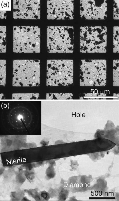
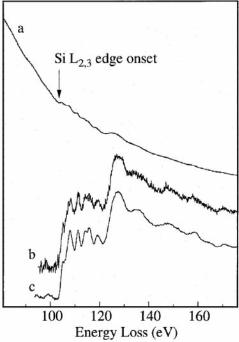
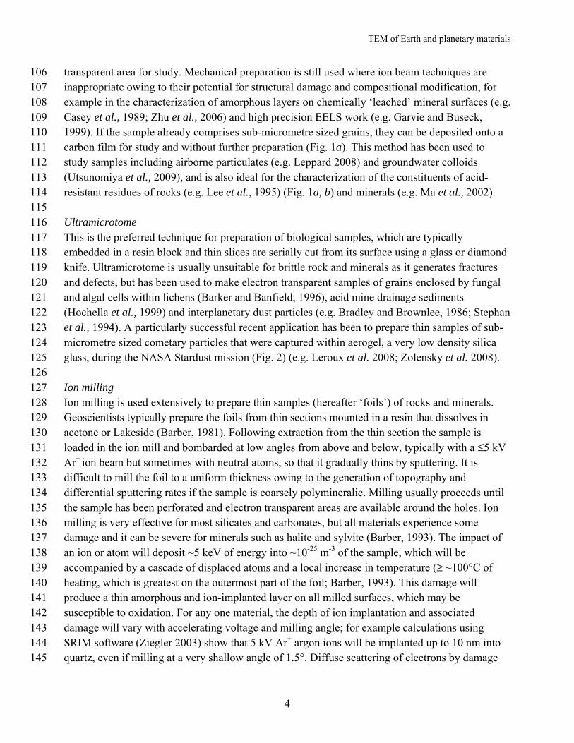
beam (FIB) technique, which is used to prepare the very thin samples required for (S)TEM from 66 specific sites on the surface of samples ranging from rough grains to polished thin sections. FIB 67 technology has revitalized interest in (S)TEM amongst geoscientists as the two techniques in 68 combination represent a ‘microstructural microprobe’. This is because they enable comprehensive 69 characterization of thin samples that can be extracted from the bulk material with the same spatial 70 accuracy (i.e. better than a few micrometres) as analyses by techniques including electron probe 71 microanalysis (EMPA) and secondary ion mass spectrometry. The second technical development 72 is electron backscatter diffraction (EBSD), which is a SEM based method whereby electron 73 backscatter (Kikuchi) patterns are obtained from polished samples of rocks and minerals for 74 quantitative characterization of their microtextures (Prior et al. 1999). The dramatic increase over 75 the last decade in rates of Kikuchi pattern acquisition, and the development of sophisticated 76 software for pattern indexing and data presentation, has stimulated microstructural research in 77 areas ranging from structural geology to biomineralization. Whilst not directly related to (S)TEM, 78 this increasing volume of research has drawn new attention to the wealth of information on 79 crystallization, alteration and deformation that can be obtained from the microstructures and 80 microtextures of rocks and minerals. In fact, EBSD has supplanted (S)TEM in some applications, 81 such as visualizing deformation within single crystals (Reddy et al., 2006), mapping the textures 82 of polycrystalline samples over tens of micrometre scales (e.g. Watt et al., 2006), and facilitating 83 the non-destructive identification of new minerals (Mikouchi et al., 2009), but the two techniques 84 are particularly powerful when used together (e.g. Lee and Ellen, 2008). 85 86 Which method of sample preparation? 87 One of the principal hurdles to the more widespread use of (S)TEM by geoscientists has been 88 sample preparation. The challenge is to render the sample sufficiently thin so that when irradiated 89 with a ~100-300 kV electron beam the incident electrons can pass through the sample and without 90 being scattered too highly or losing a significant proportion of their initial energy. A suitably thin 91 sample is often termed ‘electron transparent’. The target thickness is dependent on the material 92 and the application. For general TEM imaging and electron diffraction work on silicate minerals 93 ~100 nm is acceptable, but for analysis by EELS the samples should contain areas that are thinner 94 (<~50 nm), and atomic resolution TEM imaging requires regions that are ≤~10 nm thick and free 95 of damage to their crystal structure. As lenses are not used to form STEM images, the thickness 96 requirements for STEM samples are typically less stringent than for TEM. Below are described the 97 four main ways in which electron-transparent samples can be prepared from Earth and planetary 98 materials. 99 100 Mechanical and chemical comminution 101 The main method for producing electron transparent samples of insulators prior to the 102 development of ion milling in the 1970s (e.g. Barber 1970) was grinding them to a powder. 103 Typically the sample is crushed, or a specific region abraded using a drill, and the powder 104 deposited on a carbon film (Fig. 1a); some of the constituent grains will have sufficient electron 105
TEM of Earth and planetary materials
4
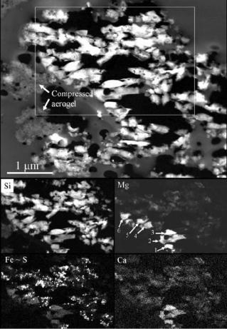
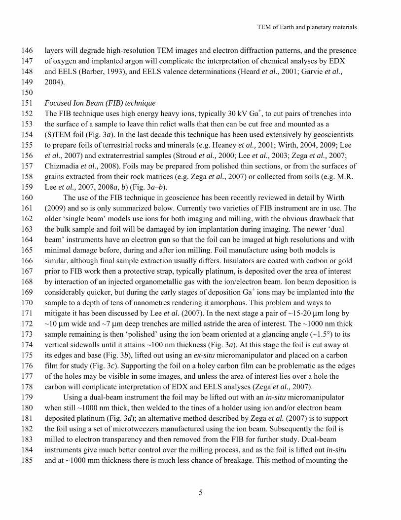
transparent area for study. Mechanical preparation is still used where ion beam techniques are 106 inappropriate owing to their potential for structural damage and compositional modification, for 107 example in the characterization of amorphous layers on chemically ‘leached’ mineral surfaces (e.g. 108 Casey et al., 1989; Zhu et al., 2006) and high precision EELS work (e.g. Garvie and Buseck, 109 1999). If the sample already comprises sub-micrometre sized grains, they can be deposited onto a 110 carbon film for study and without further preparation (Fig. 1a). This method has been used to 111 study samples including airborne particulates (e.g. Leppard 2008) and groundwater colloids 112 (Utsunomiya et al., 2009), and is also ideal for the characterization of the constituents of acid-113 resistant residues of rocks (e.g. Lee et al., 1995) (Fig. 1a, b) and minerals (e.g. Ma et al., 2002). 114 115 Ultramicrotome 116 This is the preferred technique for preparation of biological samples, which are typically 117 embedded in a resin block and thin slices are serially cut from its surface using a glass or diamond 118 knife. Ultramicrotome is usually unsuitable for brittle rock and minerals as it generates fractures 119 and defects, but has been used to make electron transparent samples of grains enclosed by fungal 120 and algal cells within lichens (Barker and Banfield, 1996), acid mine drainage sediments 121 (Hochella et al., 1999) and interplanetary dust particles (e.g. Bradley and Brownlee, 1986; Stephan 122 et al., 1994). A particularly successful recent application has been to prepare thin samples of sub-123 micrometre sized cometary particles that were captured within aerogel, a very low density silica 124 glass, during the NASA Stardust mission (Fig. 2) (e.g. Leroux et al. 2008; Zolensky et al. 2008). 125 126 Ion milling 127 Ion milling is used extensively to prepare thin samples (hereafter ‘foils’) of rocks and minerals. 128 Geoscientists typically prepare the foils from thin sections mounted in a resin that dissolves in 129 acetone or Lakeside (Barber, 1981). Following extraction from the thin section the sample is 130 loaded in the ion mill and bombarded at low angles from above and below, typically with a ≤5 kV 131 Ar+ ion beam but sometimes with neutral atoms, so that it gradually thins by sputtering. It is 132 difficult to mill the foil to a uniform thickness owing to the generation of topography and 133 differential sputtering rates if the sample is coarsely polymineralic. Milling usually proceeds until 134 the sample has been perforated and electron transparent areas are available around the holes. Ion 135 milling is very effective for most silicates and carbonates, but all materials experience some 136 damage and it can be severe for minerals such as halite and sylvite (Barber, 1993). The impact of 137 an ion or atom will deposit ~5 keV of energy into ~10-25 m-3 of the sample, which will be 138 accompanied by a cascade of displaced atoms and a local increase in temperature (≥ ~100°C of 139 heating, which is greatest on the outermost part of the foil; Barber, 1993). This damage will 140 produce a thin amorphous and ion-implanted layer on all milled surfaces, which may be 141 susceptible to oxidation. For any one material, the depth of ion implantation and associated 142 damage will vary with accelerating voltage and milling angle; for example calculations using 143 SRIM software (Ziegler 2003) show that 5 kV Ar+ argon ions will be implanted up to 10 nm into 144 quartz, even if milling at a very shallow angle of 1.5°. Diffuse scattering of electrons by damage 145
TEM of Earth and planetary materials
5
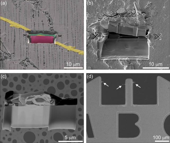
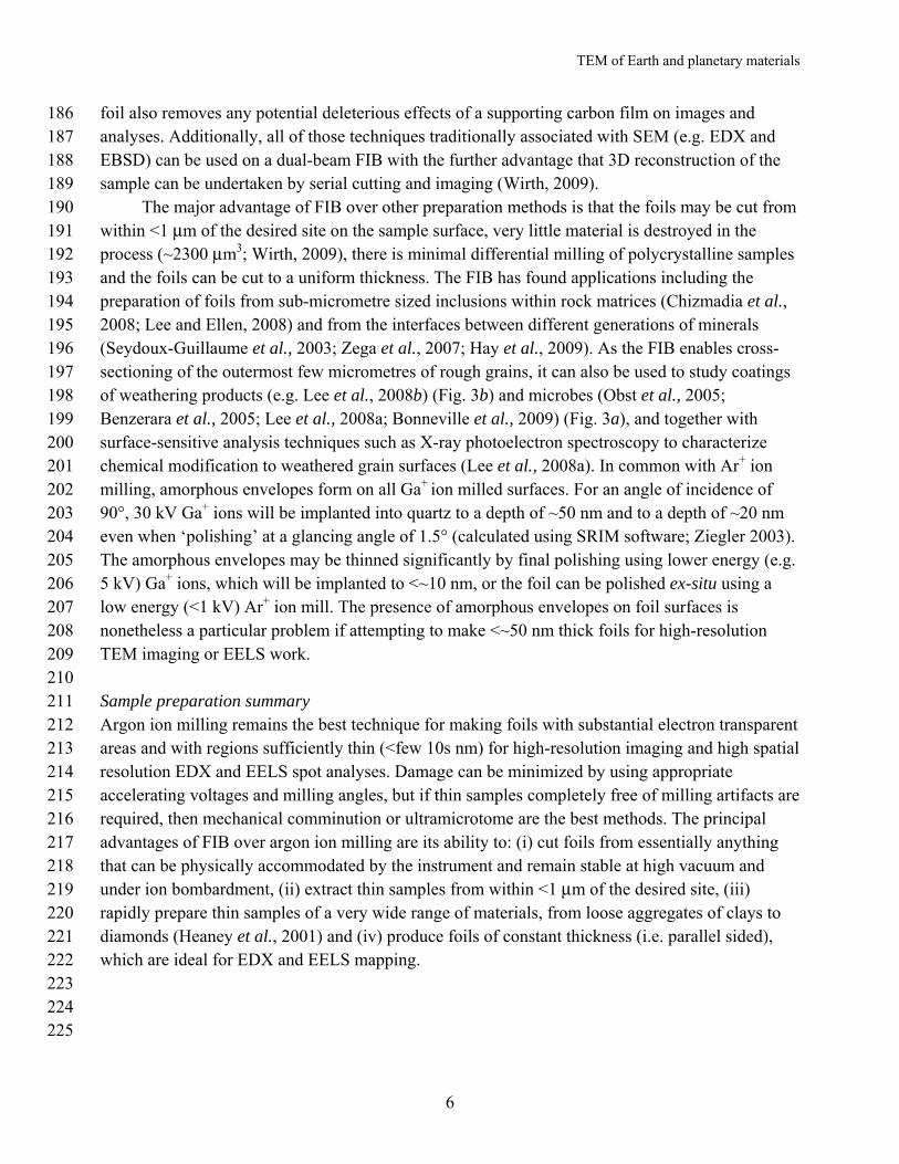
layers will degrade high-resolution TEM images and electron diffraction patterns, and the presence 146 of oxygen and implanted argon will complicate the interpretation of chemical analyses by EDX 147 and EELS (Barber, 1993), and EELS valence determinations (Heard et al., 2001; Garvie et al., 148 2004). 149 150 Focused Ion Beam (FIB) technique 151 The FIB technique uses high energy heavy ions, typically 30 kV Ga+, to cut pairs of trenches into 152 the surface of a sample to leave thin relict walls that then can be cut free and mounted as a 153 (S)TEM foil (Fig. 3a). In the last decade this technique has been used extensively by geoscientists 154 to prepare foils of terrestrial rocks and minerals (e.g. Heaney et al., 2001; Wirth, 2004, 2009; Lee 155 et al., 2007) and extraterrestrial samples (Stroud et al., 2000; Lee et al., 2003; Zega et al., 2007; 156 Chizmadia et al., 2008). Foils may be prepared from polished thin sections, or from the surfaces of 157 grains extracted from their rock matrices (e.g. Zega et al., 2007) or collected from soils (e.g. M.R. 158 Lee et al., 2007, 2008a, b) (Fig. 3a–b). 159 The use of the FIB technique in geoscience has been recently reviewed in detail by Wirth 160 (2009) and so is only summarized below. Currently two varieties of FIB instrument are in use. The 161 older ‘single beam’ models use ions for both imaging and milling, with the obvious drawback that 162 the bulk sample and foil will be damaged by ion implantation during imaging. The newer ‘dual 163 beam’ instruments have an electron gun so that the foil can be imaged at high resolutions and with 164 minimal damage before, during and after ion milling. Foil manufacture using both models is 165 similar, although final sample extraction usually differs. Insulators are coated with carbon or gold 166 prior to FIB work then a protective strap, typically platinum, is deposited over the area of interest 167 by interaction of an injected organometallic gas with the ion/electron beam. Ion beam deposition is 168 considerably quicker, but during the early stages of deposition Ga+ ions may be implanted into the 169 sample to a depth of tens of nanometres rendering it amorphous. This problem and ways to 170 mitigate it has been discussed by Lee et al. (2007). In the next stage a pair of ~15-20 μm long by 171 ~10 μm wide and ~7 μm deep trenches are milled astride the area of interest. The ~1000 nm thick 172 sample remaining is then ‘polished’ using the ion beam oriented at a glancing angle (~1.5°) to its 173 vertical sidewalls until it attains ~100 nm thickness (Fig. 3a). At this stage the foil is cut away at 174 its edges and base (Fig. 3b), lifted out using an ex-situ micromanipulator and placed on a carbon 175 film for study (Fig. 3c). Supporting the foil on a holey carbon film can be problematic as the edges 176 of the holes may be visible in some images, and unless the area of interest lies over a hole the 177 carbon will complicate interpretation of EDX and EELS analyses (Zega et al., 2007). 178 Using a dual-beam instrument the foil may be lifted out with an in-situ micromanipulator 179 when still ~1000 nm thick, then welded to the tines of a holder using ion and/or electron beam 180 deposited platinum (Fig. 3d); an alternative method described by Zega et al. (2007) is to support 181 the foil using a set of microtweezers manufactured using the ion beam. Subsequently the foil is 182 milled to electron transparency and then removed from the FIB for further study. Dual-beam 183 instruments give much better control over the milling process, and as the foil is lifted out in-situ 184 and at ~1000 mm thickness there is much less chance of breakage. This method of mounting the 185
TEM of Earth and planetary materials
6
foil also removes any potential deleterious effects of a supporting carbon film on images and 186 analyses. Additionally, all of those techniques traditionally associated with SEM (e.g. EDX and 187 EBSD) can be used on a dual-beam FIB with the further advantage that 3D reconstruction of the 188 sample can be undertaken by serial cutting and imaging (Wirth, 2009). 189 The major advantage of FIB over other preparation methods is that the foils may be cut from 190 within <1 μm of the desired site on the sample surface, very little material is destroyed in the 191 process (~2300 μm3; Wirth, 2009), there is minimal differential milling of polycrystalline samples 192 and the foils can be cut to a uniform thickness. The FIB has found applications including the 193 preparation of foils from sub-micrometre sized inclusions within rock matrices (Chizmadia et al., 194 2008; Lee and Ellen, 2008) and from the interfaces between different generations of minerals 195 (Seydoux-Guillaume et al., 2003; Zega et al., 2007; Hay et al., 2009). As the FIB enables cross-196 sectioning of the outermost few micrometres of rough grains, it can also be used to study coatings 197 of weathering products (e.g. Lee et al., 2008b) (Fig. 3b) and microbes (Obst et al., 2005; 198 Benzerara et al., 2005; Lee et al., 2008a; Bonneville et al., 2009) (Fig. 3a), and together with 199 surface-sensitive analysis techniques such as X-ray photoelectron spectroscopy to characterize 200 chemical modification to weathered grain surfaces (Lee et al., 2008a). In common with Ar+ ion 201 milling, amorphous envelopes form on all Ga+ ion milled surfaces. For an angle of incidence of 202 90°, 30 kV Ga+ ions will be implanted into quartz to a depth of ~50 nm and to a depth of ~20 nm 203 even when ‘polishing’ at a glancing angle of 1.5° (calculated using SRIM software; Ziegler 2003). 204 The amorphous envelopes may be thinned significantly by final polishing using lower energy (e.g. 205 5 kV) Ga+ ions, which will be implanted to <~10 nm, or the foil can be polished ex-situ using a 206 low energy (<1 kV) Ar+ ion mill. The presence of amorphous envelopes on foil surfaces is 207 nonetheless a particular problem if attempting to make <~50 nm thick foils for high-resolution 208 TEM imaging or EELS work. 209 210 Sample preparation summary 211 Argon ion milling remains the best technique for making foils with substantial electron transparent 212 areas and with regions sufficiently thin (<few 10s nm) for high-resolution imaging and high spatial 213 resolution EDX and EELS spot analyses. Damage can be minimized by using appropriate 214 accelerating voltages and milling angles, but if thin samples completely free of milling artifacts are 215 required, then mechanical comminution or ultramicrotome are the best methods. The principal 216 advantages of FIB over argon ion milling are its ability to: (i) cut foils from essentially anything 217 that can be physically accommodated by the instrument and remain stable at high vacuum and 218 under ion bombardment, (ii) extract thin samples from within <1 μm of the desired site, (iii) 219 rapidly prepare thin samples of a very wide range of materials, from loose aggregates of clays to 220 diamonds (Heaney et al., 2001) and (iv) produce foils of constant thickness (i.e. parallel sided), 221 which are ideal for EDX and EELS mapping. 222 223 224 225
TEM of Earth and planetary materials
7
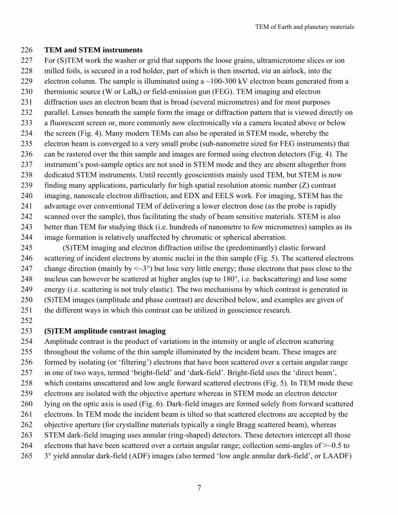
TEM and STEM instruments 226 For (S)TEM work the washer or grid that supports the loose grains, ultramicrotome slices or ion 227 milled foils, is secured in a rod holder, part of which is then inserted, via an airlock, into the 228 electron column. The sample is illuminated using a ~100-300 kV electron beam generated from a 229 thermionic source (W or LaB6) or field-emission gun (FEG). TEM imaging and electron 230 diffraction uses an electron beam that is broad (several micrometres) and for most purposes 231 parallel. Lenses beneath the sample form the image or diffraction pattern that is viewed directly on 232 a fluorescent screen or, more commonly now electronically via a camera located above or below 233 the screen (Fig. 4). Many modern TEMs can also be operated in STEM mode, whereby the 234 electron beam is converged to a very small probe (sub-nanometre sized for FEG instruments) that 235 can be rastered over the thin sample and images are formed using electron detectors (Fig. 4). The 236 instrument’s post-sample optics are not used in STEM mode and they are absent altogether from 237 dedicated STEM instruments. Until recently geoscientists mainly used TEM, but STEM is now 238 finding many applications, particularly for high spatial resolution atomic number (Z) contrast 239 imaging, nanoscale electron diffraction, and EDX and EELS work. For imaging, STEM has the 240 advantage over conventional TEM of delivering a lower electron dose (as the probe is rapidly 241 scanned over the sample), thus facilitating the study of beam sensitive materials. STEM is also 242 better than TEM for studying thick (i.e. hundreds of nanometre to few micrometres) samples as its 243 image formation is relatively unaffected by chromatic or spherical aberration. 244 (S)TEM imaging and electron diffraction utilise the (predominantly) elastic forward 245 scattering of incident electrons by atomic nuclei in the thin sample (Fig. 5). The scattered electrons 246 change direction (mainly by <~3°) but lose very little energy; those electrons that pass close to the 247 nucleus can however be scattered at higher angles (up to 180°, i.e. backscattering) and lose some 248 energy (i.e. scattering is not truly elastic). The two mechanisms by which contrast is generated in 249 (S)TEM images (amplitude and phase contrast) are described below, and examples are given of 250 the different ways in which this contrast can be utilized in geoscience research. 251 252 (S)TEM amplitude contrast imaging 253 Amplitude contrast is the product of variations in the intensity or angle of electron scattering 254 throughout the volume of the thin sample illuminated by the incident beam. These images are 255 formed by isolating (or ‘filtering’) electrons that have been scattered over a certain angular range 256 in one of two ways, termed ‘bright-field’ and ‘dark-field’. Bright-field uses the ‘direct beam’, 257 which contains unscattered and low angle forward scattered electrons (Fig. 5). In TEM mode these 258 electrons are isolated with the objective aperture whereas in STEM mode an electron detector 259 lying on the optic axis is used (Fig. 6). Dark-field images are formed solely from forward scattered 260 electrons. In TEM mode the incident beam is tilted so that scattered electrons are accepted by the 261 objective aperture (for crystalline materials typically a single Bragg scattered beam), whereas 262 STEM dark-field imaging uses annular (ring-shaped) detectors. These detectors intercept all those 263 electrons that have been scattered over a certain angular range; collection semi-angles of >~0.5 to 264 3° yield annular dark-field (ADF) images (also termed ‘low angle annular dark-field’, or LAADF) 265
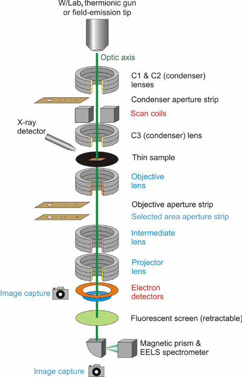
TEM of Earth and planetary materials
8
whereas semi-angles of ~3 to 10° provide high angle annular dark-field (HAADF) images (Fig. 6). 266 The distinction between LAADF and HAADF may be made by using separate detectors (Fig. 6), 267 or by changing the diffraction camera length (effectively the magnification of the diffraction 268 pattern) so that different angular ranges can be captured using a single fixed annular detector. 269 Three properties of a thin sample will determine the intensity and angle of scattering of the 270 incident beam and so its appearance in bright- and dark-field images: thickness (t) and atomic 271 mass (Z) (together termed mass-thickness contrast), and Bragg diffraction (only in crystalline 272 materials). The ways in which these properties produce contrast that is useful to the geoscientist 273 are described below. 274 275 Mass-thickness contrast 276 Mass-thickness contrast is an outcome of incoherent elastic scattering of incident electrons by the 277 thin sample, the intensity of which increases with both Z and t. Thus, thicker and higher Z regions 278 of a sample will be relatively dark in bright-field images because a high proportion of incident 279 electrons are being scattered, thus lowering the intensity of the direct beam. Thickness contrast is 280 most important at scattering angles of <5° (Williams and Carter, 1996) and has few geoscience 281 applications, although dark and bright bands produced by thickness variation (i.e. thickness 282 fringes) are characteristic of the wedge-shaped edges of thin samples. Z contrast imaging is much 283 more useful in geoscience and utilizes electrons that have undergone high angle (Rutherford) 284 scattering. At scattering semi-angles of >~3-5° Z contrast dominates over thickness contrast and, 285 crucially, electrons that have been Bragg scattered by crystalline material are absent. Although 286 LAADF can be used, contrast in these images may still have a contribution from Bragg scattering, 287 and so Z contrast imaging of crystalline samples is most effective using HAADF. As the intensity 288 of Rutherford scattering is proportional to Z1.7-2 (Muller, 2009), HAADF images can be 289 qualitatively interpreted in the same way as those obtained from a SEM backscattered electron 290 detector (Figs 2, 7a–b). As the size of the probes used in modern field-emission STEM 291 instruments (typically sub-nanometre, with ~0.05 nm probes available on microscopes with 292 aberration corrected probe-forming optics; Muller, 2009) are considerably smaller than the spacing 293 of atom columns, atomic resolution HAADF images can be obtained by very fine-scale scanning 294 of the probe over a thin sample oriented with atom columns parallel to the microscope optic axis 295 (Fig. 7c). Atom columns scatter electrons more strongly than inter-atomic areas and so appear 296 bright (high signal intensity) in the HAADF images. Using this technique single dopant atoms in 297 synthetic materials have been detected (Muller, 2009) and as the aberration corrected STEM has a 298 very small depth of focus, by collecting through-focus images it is possible to locate individual 299 impurity atoms within amorphous and crystalline materials in three-dimensions (Xin et al., 2008). 300 Owing to the Z dependence of high angle scattering, columns of atoms with different atomic 301 numbers can be recognized in HAADF images, although low Z atoms such as oxygen can be hard 302 to identify. Sample requirements for atomic resolution HAADF are stringent (clean, free of 303 preparation artifacts and <20 nm thick), although less exacting than for atomic resolution TEM 304 imaging (i.e. high-resolution HAADF is less sensitive to sample thickness and focus). In addition 305
TEM of Earth and planetary materials
9
HAADF images can be understood without the numerical simulations required to correctly 306 interpret the crystal structures seen in high-resolution TEM (Bleloch and Lupini, 2004). 307 HAADF is a very useful tool for characterizing the constituents of finely polymineralic 308 samples, especially where the minerals of interest have a significantly greater Z than their matrix. 309 Examples of such applications are locating few nanometre sized uraninite grains within 310 atmospheric aerosols (Utsunomiya and Ewing, 2003), finding ~5-10 nm sized gold nanoparticles 311 within pyrite (Palenik et al., 2004) and identifying radionuclide bearing nanoparticles 312 (Utsunomiya et al., 2009). Zega et al. (2007), Chizmadia et al. (2008) and Bland et al. (2009) have 313 also used HAADF to characterise FIB-produced foils of the very finely crystalline matrices of 314 carbonaceous chondrite meteorites, which contain Fe,Ni metal and Fe-sulphide grains embedded 315 within a lower Z silicate groundmass (Fig. 7a-b). Very fine scale mineral mixtures were studied 316 during investigation of cometary particles collected by the NASA Stardust mission (Fig. 2). 317 Atomic resolution HAADF has yet to find many applications in geoscience, but Utsunomiya et al. 318 (2004) showed how it could be used to help locate lead within zircon. They showed that the lead 319 was concentrated in ~5 nm sized crystalline patches (within which it had substituted for zirconium; 320 Fig. 7c) and had also diffused into the amorphous material of a fission track. Although potential 321 sites of lead accumulation had been located by HAADF imaging, EDX was needed to 322 unequivocally identify lead within the columns of higher Z atoms (Utsunomiya et al., 2004). 323 324 Diffraction contrast 325 Diffraction contrast is an outcome of coherent elastic scattering of incident electrons and enables: 326 (i) discrimination of amorphous from crystalline regions within a crystal, (ii) visualisation of intra- 327 and inter-crystalline orientation differences, and (iii) identification of mineral inclusions by their 328 contrasting diffraction properties to the host crystal. As it is weak or absent in STEM images, 329 diffraction contrast imaging is mainly exploited by bright- and dark-field TEM. For incident 330 electrons to be Bragg scattered (diffracted) by a crystal, one or more sets of its lattice planes must 331 be oriented relative to the incident electron beam at the Bragg angle (typically <1º). If the crystal is 332 oriented with a major zone axis (i.e. several sets of atomic planes) parallel to the optic axis of the 333 microscope a high proportion of electrons will be Bragg scattered and so a bright-field image will 334 be dark and with little contrast. Image contrast can be increased to reveal intracrystalline 335 microtextures, or microstructures defined by local variations in orientation or unit-cell parameters 336 by tilting away from the zone axis (Fig. 8a). 337 TEM diffraction contrast imaging remains the most useful technique for high magnification 338 (although not high resolution) characterization of microstructures and microtextures (Champness, 339 1997; Putnis, 1992). Amorphous regions within a crystal can be readily identified using bright-340 field TEM by their absence of Bragg diffraction in comparison to the crystalline host, for example 341 shock lamellae within silicate minerals from terrestrial impact craters and meteorites (e.g. Leroux, 342 2001) and amorphous layers on weathered silicates (Lee et al., 2008a, b). Diffraction contrast is 343 also the primary means of imaging twins, exsolution lamellae (e.g. Brown and Parsons, 1984; Fitz 344 Gerald et al., 2006) (Fig. 8a) and subgrains (Lee and Parsons, 2003; Fig. 8b). Crucially however, 345
TEM of Earth and planetary materials
10
as the Bragg angle is so small, the technique is highly sensitive to tiny (fractions of a degree) 346 intracrystalline orientation differences. These may arise due to elastic strain induced by 347 precipitates, vacancies and dislocations (e.g. Leroux, 2001) or the very-fine scale intergrowths of 348 domains formed by processes such as spinoidal decomposition (e.g. tweed orthoclase). Although 349 such orientation sensitivity can be highly beneficial, even a slight warping of the thin sample will 350 result in significant variations it the angle it makes with the incident beam so that the Bragg 351 condition may be satisfied only locally, producing ‘bend contours’ (Fig. 8b). 352 353 TEM phase contrast imaging 354 Phase contrast is present in all (S)TEM images and is formed by the interference of electron waves 355 that have been scattered by the sample and are out of phase. By optimizing phase over amplitude 356 contrast, images can be obtained that contain information on the periodicity and orientations of 357 one or more sets of atomic planes (lattice images), and that can be interpreted to reveal the 358 positions of atom columns. To form these high-resolution images the area of interest should be as 359 thin as possible (ideally <~8 nm for imaging atoms in a medium Z material at 200 kV; Williams 360 and Carter, 1996) and oriented with a zone axis precisely on the microscope’s optic axis. The 361 electron beam should also be aligned to the optic axis and a relatively large objective aperture used 362 so that the image is formed from the direct beam, diffracted beams and electrons elastically and 363 inelastically scattered between them. 364 Lattice fringe imaging uses the direct beam and one or more diffracted beams and each set of 365 fringes in the image represents a set of atomic planes whose Bragg scattered electrons have been 366 accepted by the aperture. Modern TEMs can readily form such images with a <0.1 nm line 367 resolution (Smith, 2008) and the technique is not as demanding on sample thickness or defocus 368 setting as structure imaging (see below). Lattice fringe images provide detailed information on 369 local crystal structure and orientation (Fig. 9), but crucially the fringes cannot usually be 370 interpreted as direct representations of atomic planes. Nonetheless, lattice fringe imaging is used 371 extensively in geoscience, especially in studies of minerals with relatively large d-spacings such as 372 clays and phyllosilicates and a key application has been to visualize the orientation relationships of 373 the constituents of finely polycrystalline samples such as mudrocks (e.g. Peacor, 1992a). A good 374 example of the power of lattice fringe imaging is illustrated by Banfield and Barker (1994), who 375 were able to demonstrate that structural inheritance plays an important role in the replacement of 376 amphibole by smectite during weathering (Fig. 9). 377 In order to obtain high-resolution images that can be interpreted to reveal the locations of 378 individual atom columns or groups of columns it is necessary to use a large objective aperture that 379 accepts many diffracted beams. To simplify image interpretation, only beams diffracted from those 380 atomic planes whose d-spacings are greater than the point-to-point resolution of the microscope 381 should be used. Under these conditions images (usually series of images) can be obtained that 382 contain a representation of the crystal structure, but in order to interpret features as atoms or 383 groups of atoms it is necessary to use computer programmes to simulate the crystal structure 384 expected when looking down the relevant zone axis and given the appropriate values for defocus 385
TEM of Earth and planetary materials
11
and sample thickness (Self, 1992). This technique is used much less frequently in geoscience than 386 lattice fringe imaging due to a combination of reasons including the specialist skills and equipment 387 required to acquire and correctly interpret the results, and limitations imposed by damage to the 388 thin sample. One example is the characterization of fibrous inclusions in quartz. Ma et al. (2002) 389 extracted fibers from sample of rose quartz using HF acid, then by using a combination of electron 390 diffraction techniques (Fig. 10a), X-ray analysis and high-resolution imaging (Fig. 10a–b), they 391 found that the fibers are very similar in crystal structure and composition to dumortierite, an 392 aluminium borosilicate. It was necessary to use computer simulations to interpret correctly the 393 crystal structures observed in high-resolution TEM images (Fig. 10a–b). 394
Atomic-resolution TEM imaging is significantly limited by spherical aberrations of the 395 defocused objective (image-forming) lenses and the wavelength spread of the incident beam 396 (producing chromatic aberration). A great deal of effort has been spent on reducing the loss of 397 information by spherical aberration so that the specimen exit plane wavefunction (EPWF) can be 398 reconstructed or retrieved. Successful application of these techniques can yield sub-Ångstrom (i.e. 399 <0.1 nm) resolution images whereby the positions of atoms can be measured to precisions of tens 400 of picometres (Hetherington, 2004; Houben et al., 2006; Urban, 2008, 2009). One method is to 401 acquire a series of 10-20 images at slightly different levels of objective lens defocus, each of 402 which will contain a subtly different set of aberrations (Kirkland and Meyer, 2004). By 403 computationally processing each aberrated image the EPWF can be reconstructed and atomic 404 resolution images produced. The other way to reduce spherical aberration is to introduce lenses 405 into the microscope column that effectively ‘reverse’ aberrations imposed by the objective lens. 406 Single images containing readily interpretable atomic positions may be obtained using aberration 407 corrected TEMs (Kirkland et al., 2008), and although EPWF reconstruction techniques are still 408 often required they are computationally more straightforward than for images obtained using non-409 corrected microscopes (Kirkland and Meyer, 2004; Urban, 2008, 2009). The driver for sub-410 Ångstrom resolution imaging has been characterization of advanced functional materials such as 411 superconductors (Urban, 2009) and these techniques are unlikely to see widespread use in 412 geoscience, especially given the stringent requirements for the thickness of a sample and its 413 stability under the high current densities used for illuminating very small sample volumes. 414 415 (S)TEM electron diffraction 416 Diffraction patterns record the angular distribution of electrons that have been coherently 417 elastically scattered by the thin sample and by <~3°. Amorphous materials produce patterns with 418 diffuse intensity variations whereas single crystals yield periodic arrays of spots generated by 419 Bragg scattering. Spot patterns are effectively a two dimensional section through the reciprocal 420 lattice of the crystal and the positions of spots are determined by the separation (d-spacing) of 421 atomic planes and their orientation. The TEM based technique of selected area electron diffraction 422 (SAED) is used most widely in geoscience, but other methods including precession electron 423 diffraction, convergent beam electron diffraction and electron nanodiffraction have specific 424 applications. 425
TEM of Earth and planetary materials
12
For SAED the foil is illuminated using a broad and parallel electron beam and the region 426 from where the diffraction pattern is required is defined using the selected area aperture; the 427 smallest area selectable is ~500 nm in diameter. If one crystal is present, and oriented with several 428 sets of atomic planes (i.e. a zone axis) at the Bragg angle relative to the incident beam, a single 429 array of spots is formed (Fig. 1b). A SAED pattern from two or more crystals will yield 430 superimposed patterns and a region containing many crystals in random orientations relative to 431 each other will generate a large number of spots that merge into continuous rings (Fig. 1b). In 432 geoscience SAED is used most commonly to: (i) to help identify minerals and (ii) determine the 433 orientation of the thin sample and the crystallographic orientations of grain boundaries and 434 intracrystalline features including dislocations, twin composition planes and exsolution lamellae. 435
Minerals can be identified using the spacings of spots, supported by information on the 436 angles between diffracting planes, and pattern symmetry of can also provide a guide to the crystal 437 system. SAED is inferior to X-ray diffraction (XRD) in the accuracy and precision of d-spacing 438 measurements. However, with careful calibration of the camera factor (essentially the 439 magnification of the SAED pattern) and correction for elliptical distortion, accuracies and 440 precisions of 0.1% in d-spacing determinations can be achieved (Steeds and Morniroli, 1992; 441 Mugnaioli et al. 2009). For such work it is desirable to deposit a standard such as sputtered gold 442 onto the thin sample to give rings of known d-spacing superimposed on the diffraction pattern of 443 the sample. Mugnaioli et al. (2009) note that although an accuracy of 0.1% is achievable, d-444 spacings of any one crystal may vary by > 0.1% owing to intracrystalline compositional 445 heterogeneities; dehydration under vacuum and ion and electron beam damage may also modify 446 the original d-spacings of minerals including micas and phyllosilicates. To determine the 447 approximate orientations of features in an image, crystallographic directions obtained from an 448 indexed SAED pattern are plotted on its corresponding image (after correction for any magnetic 449 rotation between the two). However, in order to establish the absolute orientation ‘trace analysis’ 450 needs to be undertaken using several diffraction pattern-image pairs (e.g. Loretto, 1994). 451 Recently a variant of SAED termed precession electron diffraction (PED) has become 452 commercially available and enables a much more sophisticated interpretation of spot patterns 453 derived from single crystals. PED requires a modified TEM and is undertaken by precessing the 454 electron beam around the optic axis of the microscope (Jacob et al.,, 2009). The resulting patterns 455 contain spots whose intensities (in addition to d-spacings and angles) can be used to undertake 456 sophisticated crystallographic analysis including crystal structure determinations and assessment 457 of bonding (Avilov et al., 2007). Electron crystallography by PED offers a clear advantage over X-458 ray crystallography because structure determinations can be done on much smaller crystals than 459 can be effectively studied by X-ray diffraction (Avilov et al., 2007). Although few suitably 460 equipped microscopes are currently available, the ease of use of PED coupled with the detailed 461 information it can provide, mean that it is likely to find many future applications in mineralogy 462 (e.g. Jacob et al., 2009). Convergent beam electron diffraction (CBED) patterns are best acquired 463 from crystals with a low defect density and are formed using a focused electron probe (and a large 464 condenser aperture) so that the size of the diffracting volume is essentially determined by the 465
TEM of Earth and planetary materials
13
dimensions of the electron beam. Thus, CBED patterns can be obtained from ~10 nm sized 466 regions. The patterns contain discs of intensity, as opposed to the spots of SAED, and the structure 467 of the discs contains a wealth of crystallographic information unobtainable by conventional SAED 468 including point and space group (Steeds and Morniroli, 1992), and CBED also enables crystal 469 structure refinements (e.g. Beermann and Brockamp, 2005). Using the very small probe available 470 in STEM, electron nanodiffraction (END) patterns can be acquired from sub-nanometre sized 471 regions of a sample (Cowley, 2004). These patterns again contain discs of intensity rather than 472 sharp spots (Fig. 11), but are indexed in the same way as SAED patterns. Janney et al. (2000, 473 2001) estimated that the error in determination of unit-cell dimensions by END was <~5%. By 474 scanning the probe over the sample and acquiring END patterns at each point, this technique can 475 be used to obtain nanoscale structural information (Janney et al., 2000, 2001). A drawback of 476 END is that the crystals cannot be tilted during experiments so that many of the patterns acquired 477 from a polycrystalline sample will not be oriented precisely on a zone axis. As with all work using 478 a fine probe, electron beam damage is a severe limitation and kaolinite for example can turn 479 amorphous in less than one second (Fig. 11). 480
Geoscientists are now also making extensive use of Fourier transforms of high-resolution 481 (S)TEM images to obtain information on orientations and spacings of atomic planes. This 482 technique converts the periodicity of a high-resolution digital image into a diffractogram that can 483 be indexed in the same way as a SAED pattern to: (i) help identify minerals (e.g. Palenik et al., 484 2004; Utsunomiya et al. 2009), (ii) confirm orientation data derived from the source image (e.g. 485 Utsunomiya et al. 2004; Chizmadia and Brearley, 2008) and (iii) to assess crystallinity (Benzerara 486 et al., 2005). Diffractograms are useful because they greatly reduce the complexity of the high-487 resolution image and so can reveal features that are hard to identify visually, but in doing so 488 information may be lost and so they are not a replacement for conventional diffraction work. 489 490 Limitations to (S)TEM work by electron beam damage 491 Even before (S)TEM work is undertaken, minerals may be modified by exposure to a vacuum in 492 the ion mill, coater and (S)TEM. For example, smectite commonly dehydrates with a consequent 493 change its (001) layer spacings from ~1.5-1.2 nm to ~1.0 nm. The deleterious effects of ion 494 bombardment were described earlier, and electron beam irradiation can further alter thin samples 495 and by three mechanisms: radiolysis, heating and knock-on (or displacement) damage (Williams 496 and Carter, 1996; Egerton et al., 2004) (Fig. 12). For many minerals, electron induced sample 497 deterioration can be the principal limitation to the spatial resolution at which (S)TEM images, and 498 EDX and EELS spot analyses and maps can be acquired. 499
Radiolysis is the ionization of sample atoms during inelastic scattering and leads to breaking 500 of bonds, resulting in defect formation and amorphisation, sputtering of atoms from sample 501 surfaces and changes in chemistry (Fig. 12). Heating also takes place as energy is transferred from 502 incident electrons to sample atoms during inelastic scattering, and can be a particular problem for 503 minerals with poor thermal conductivity (Egerton et al., 2004). Breaking of bonds, vaporization 504 and chemical reactions including recrystallization are common consequences of heating (Fig. 12). 505
TEM of Earth and planetary materials
14
Silicate minerals are very prone to radiolysis and heating, but its effects may be minimised by 506 cooling the sample using liquid nitrogen or increasing accelerating voltage (Williams and Carter, 507 1996) in addition to using a broader beam (in TEM mode), or rastered beam (in STEM mode) and 508 reducing acquisition times for images, diffraction patterns and analyses. Knock-on damage is 509 mainly a consequence of momentum transfer from incident electrons to atomic nuclei during high-510 angle elastic scattering, which despite the term ‘elastic’ does involve some energy loss to incident 511 electrons. This process can lead to displacement of internal atoms, especially those of low Z, and 512 sputtering of the more weakly bonded atoms from sample surfaces (Williams and Carter, 1996; 513 Egerton et al., 2004) (Fig. 12). As the magnitude of knock-on damage increases with accelerating 514 voltage and decreases with Z and strength of atomic bonds, it can be countered by reducing kV to 515 below the displacement threshold of sample atoms, which is >200 kV for atoms of medium to high 516 Z, although those close to the sample surface will have a lower threshold (Egerton et al., 2004). 517
The susceptibility of a given sample to damage will depend on the dominant damage 518 mechanism(s) operative within the mineral of interest and under the instrumental conditions used. 519 However, beam damage is typically severe in hydrous minerals and those that are alkali-rich, 520 including feldspars (e.g. Janney and Wenk 1999; Lee et al., 2007) and the readily identifiable 521 consequences are defect formation, amorphisation, ‘drilling’ of holes (Fig. 7a–b) and changes in 522 chemical composition (see later). Carbonates are also unstable (Reeder, 1992), and in particular 523 those containing ions that have substituted for Ca2+ (Barber and Wenk, 1984), leading to the 524 formation of dislocations and bubbles. At greater degrees of damage carbonates can lose CO2, with 525 calcite recrystallizing to CaO (lime) and dolomite recrystallizing to CaO plus MgO, probably in 526 response to ionization of carbonate anions (Cater and Buseck, 1985). Lee (1993) found that 527 gypsum (CaSO4.2H2O) readily recrystallizes in the TEM, producing hemihydrite (CaSO4.0.5H2O), 528 anhydrite (CaSO4) and finally lime (CaO) over the space of a few minutes observation at 200 kV. 529 This change in crystal structure indicates progressive loss of H2O, but as EDX showed that the 530 Ca/S ratio also increased, SO2 must have been liberated (Lee, 1993). S.Lee et al. (2007) found that 531 damage can also cause kaolinite to recrystallize to polycrystalline silica as a consequence of 532 breakage and reforming of Si-O bonds. Utsunomiya et al. (2009) give a very good account of the 533 problems in trying to characterize environmental nanoparticles, some of which were extremely 534 unstable under the electron beam. 535
Another electron beam-induced artifact, which is especially problematic during EDX and 536 EELS work, is hydrocarbon contamination (Fig. 12). Hydrocarbon molecules may be deposited 537 during ion milling and coating, or derived from vapour present in the microscope column, and are 538 polymerized on the sample surface by the electron beam. This contamination can be mitigated by 539 plasma cleaning the sample and holder prior to (S)TEM work, heating/cooling the sample, or by 540 rastering the beam over the area of interest to ‘burn’ away the hydrocarbons. 541 542 Compositional analysis by (S)TEM 543 Incident electrons that interact with the electron clouds surrounding sample atoms are inelastically 544 scattered and in the process change direction (by <~1°) and lose up to ~5% of their energy. 545
TEM of Earth and planetary materials
15
Inelastic scattering provides most of the information in EELS spectra and by exciting sample 546 atoms also generates the X-rays for EDX. The EDX and EELS techniques both enable qualitative 547 and quantitative determination of elemental compositions, but EELS additionally yields 548 information on bonding and valence states. EDX analysis of thin samples is a mature and well 549 understood technique (Peacor 1992b) and geoscientists with experience of analytical SEM or 550 EPMA will be able to acquire and interpret (S)TEM X-ray analyses with little difficulty. EELS by 551 contrast is a far more specialist method, but a very powerful tool for certain applications (Buseck 552 and Self, 1992; Garvie et al., 1994; Egerton, 2009). 553 554 X-ray analysis 555 Bremsstrahlung and characteristic X-rays produced during ionization of specimen atoms can be 556 collected and their energies analysed via an energy-dispersive X-ray detector above the thin 557 sample (Fig. 4). (S)TEM-EDX differs from microanalysis of bulk materials in two important 558 respects: (i) 100-300 kV incident electrons will generate much higher energy X-rays than 20-30 559 kV electrons employed by SEM/EPMA and (ii) the volume of the sample from which X-rays are 560 generated is far smaller than in a bulk material, which is a consequence of their thickness, the 561 small incident beam diameter (quantitative analyses can be acquired from suitable samples using a 562 ~10 nm beam from a thermionic gun and a ~1 nm beam from a FEG; Williams and Carter, 1996) 563 and high electron energies (spreading of the electron beam by scattering increases with decreasing 564 electron energy and with t0.66). Spot analyses can be obtained in TEM and STEM modes although 565 element maps and spectrum maps (in which each pixel contains all the information of an emission 566 spectrum) require STEM (Fig. 2). 567 Quantitative elemental analysis by (S)TEM-EDX is simpler than for bulk materials because 568 in appropriately thin samples X-ray absorption and fluorescence can be essentially ignored (i.e. the 569 thin samples are effectively transparent to X-rays generated within them). This is called the ‘thin 570 film criterion’ (Cliff and Lorimer, 1975). As described by Peacor (1992b), (S)TEM-EDX can 571 achieve detection limits of ~0.1 wt% and yield concentrations within error of those acquired from 572 bulk samples of the same materials using EPMA. If the samples are thicker than ~50-100 nm 573 and/or low Z elements (which produce low energy X-rays) are of interest, then the thin film 574 criterion breaks down and corrections for absorption, and possibly fluorescence, must be 575 incorporated in quantification procedures (Williams and Carter, 1996). (S)TEM-EDX has been 576 used widely in geoscience and in particular for studying fine-grained rocks such as shales and 577 slates and their constituent clays and phyllosilicates, which can have considerable inter- and 578 intracrystalline compositional variation. 579 Optimising instrumental conditions for quantitative (S)TEM-EDX requires a trade-off 580 between competing variables. In the thinnest samples electron beam spreading will be at a 581 minimum, giving the highest spatial resolutions for a given probe size, but X-ray count rates will 582 be correspondingly low, possibly necessitating relatively long counting times so that specimen 583 drift (typically ~0.5 nm min-1), electron beam damage and carbon contamination may cause 584 significant problems. Damage to the sample is identifiable by hole drilling (Fig. 7a–b), although 585
TEM of Earth and planetary materials
16
element loss will occur before this is observed. For example, during STEM-EDX analysis of 586 muscovite and paragonite, Peacor (1992b) noted the loss by diffusion of K, Na and Al relative to 587 Si and Lee et al. (2007) also found rapid loss of Na and K during analysis of alkali feldspar. 588 Janney and Wenk (1999) discuss the problems in obtaining quantitative analyses of plagioclase 589 feldspar and the merits of various mitigation strategies including rastering the electron beam (in 590 STEM mode), undersaturating the electron source and cooling the specimen with liquid nitrogen. 591 Beam damage can also be alleviated by analysing thicker regions of the sample (if available), 592 which will have the additional advantage of giving greater count rates, although electron scattering 593 will increase, thus limiting spatial resolution, and absorption and fluorescence corrections may 594 have to be incorporated into quantification routines. Importantly, (S)TEM-EDX work can also 595 suffer from spurious X-rays (i.e. those derived from outside of the volume from which the analysis 596 is sought, typically the holder or even microscope components) and analyses of thin samples may 597 also contain X-rays from elements implanted during milling (e.g. argon and gallium). 598 599 EELS 600 EELS quantifies the energy lost by incident electrons during ionization of sample atoms 601 accompanying inelastic interactions, and losses range from ~5 eV to 2 KeV. The EELS detector is 602 positioned beneath the sample to collect unscattered and low angle (<1º) scattered electrons and 603 using a magnetic prism (Fig. 4) separates them according to the energy they have lost. EELS 604 measurements can be obtained by TEM or STEM, although STEM offers the significant advantage 605 that analytical work can be undertaken in parallel with LAADF/HAADF imaging. The spectra 606 obtained can be used for qualitative and quantitative analysis of elemental abundances and 607 determination of valence states and bonding of sample atoms. 608 An EELS spectrum contains three energy loss regions: (i) the zero loss peak (<5 eV), which 609 contains the direct beam and electrons that have undergone scattering but lost little energy, (ii) the 610 low loss region (5 to 50 eV) representing ionization of outer shell electrons of specimen atoms, 611 and (iii) the high loss region (50 to ~2000 eV) produced by excitation of inner shell (core) 612 electrons. The high loss region comprises a small proportion (~5%) of the net intensity of the 613 spectrum but contains a series of sharp increases in energy loss called ‘edges’. The energy loss of 614 the edge is indicative of the element present, and information on bonding and valence states comes 615 from subtle changes in the energy loss and the fine structure of the 30-50 eV long tail to the edge 616 (Garvie et al., 1994). As the intensity of the core edge of a given element is a function of the 617 number of its atoms that are present in the illuminated volume, EELS can be used to quantify 618 elemental compositions. Considerable processing may be required in order to identify edges 619 against the background and quantify their intensities (Fig. 13), but reliable data can be obtained. 620 For example, Garvie and Buseck (2004) determined concentrations of oxygen, nitrogen and 621 sulphur in <100 nm sized carbonaceous nanospheres and nanotubes from the Tagish Lake 622 (carbonaceous chondrite) meteorite. Using the energy loss of the carbon edge and its fine structure, 623 they were also able to show that the carbon had long-range order and was bonded to oxygen, 624 nitrogen and sulphur. Detailed information on Si-O bonding in crystalline and amorphous silicates 625
TEM of Earth and planetary materials
17
has also been obtained by analysis of the silicon core loss edge (Garvie and Buseck, 1999; Fig. 626 13). 627
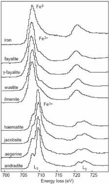
EELS has been used extensively for determining valence states of elements within minerals 628 at the few nanometre scale. Elements studied include manganese (e.g. Buseck and Self, 1992; 629 Garvie and Craven, 1994; Loomer et al., 2007), iron (e.g. Garvie and Buseck, 1998; Heard et al., 630 2001; Zega et al., 2003; Garvie et al., 2004) (Fig. 14), chromium (Garvie et al., 2004) and cerium 631 (Utsunomiya et al., 2007). Garvie and Buseck (1998) first demonstrated that the L3 edges of Fe2+ 632 and Fe3+ were sufficiently different (~1 eV) that iron valence states could readily be determined. 633 By measuring the relative heights of the two peaks the Fe3+/ΣFe values of mixed valence minerals 634 could also be quantified (Zega et al., 2003; Garvie et al., 2004). Loomer et al. (2007) used the 635 energy of the Mn L3 edge and relative intensities of the Mn L3 and L2 edges to determine average 636 manganese valence states, although were unable to distinguish Mn3+ from Mn2+ and Mn4+. 637
Using STEM, EELS analyses can be acquired at spatial resolutions of <1 nm, which is 638 superior to the resolution of STEM-EDX under comparable conditions, although such fine-scale 639 analyses can be obtained from only those materials that are sufficiently stable to withstand the 640 high beam currents required to generate a usable signal from such small volumes. By acquiring 641 spectra from grids of closely spaced points in STEM mode (i.e. spectrum mapping), images can be 642 constructed to show spatial variations in elemental abundances or even valence states. For 643 example, Loomer et al. (2007) mapped the distribution of manganese with different valence states 644 in the Mn-rich minerals braunite and bementite by acquiring a spectrum map over a 300 by 150 645 nm area at a 5 nm point spacing (and with a comparably sized probe), which took 17 minutes. The 646 acquisition times for large spectrum maps may be considerable, over which timescales the sample 647 is likely to have drifted significantly (although automatic drift correction can be used). EELS 648 acquisition times are much shorter in aberration corrected microscopes, but sample damage may 649 be severe (Muller, 2009). Garvie et al. (2004) undertook a quantitative study of the effect of 650 electron beam damage on EELS analyses of the phyllosilicate mineral cronstedtite. They found 651 that under the experimental configuration used beam damage led to loss of H with a corresponding 652 increase of Fe3+/ΣFe over their true values. It is again important to note that a significant 653 proportion of the volume of a sample sufficiently thin for good EELS work will be close to its 654 surface so that if near-surface regions have been compositionally modified during ion milling, 655 obtaining information on the elemental composition, valence and bonding that is a true reflection 656 of the original mineral may be challenging. 657 658 Energy-filtered TEM (EFTEM) imaging 659 EFTEM uses electrons from a specific region of the EELS spectrum to form an image, for 660 example the zero loss peak or one or more core loss edges. Those images formed using the zero-661 loss peak will be free of inelastically scattered electrons and so this technique is especially useful 662 for studying thick samples, TEM images from which would otherwise suffer significantly from 663 chromatic aberration. Using the core loss edges enables chemical imaging and this method has the 664 major advantage over point-by-point X-ray or EELS mapping that the images can be acquired 665
TEM of Earth and planetary materials
18
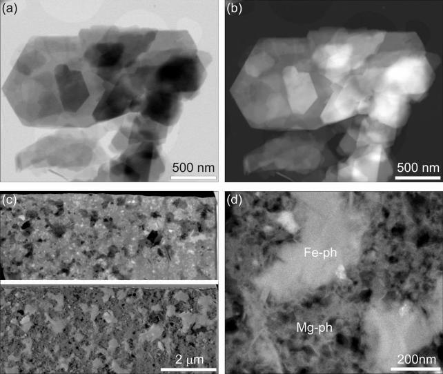
rapidly (seconds to a few minutes) and with sub-nanometre spatial resolutions (Grogger et al., 666 2003). EFTEM chemical imaging has been used in applications including characterizing finely 667 polymineralic acid mine drainage samples (Hochella et al., 1999), observing oxygen enrichment in 668 the rims of meteoritic Fe,Ni metal grains (Chizmadia et al., 2008) and mapping the distribution of 669 manganese and iron within desert varnish (Garvie et al., 2008) (Fig. 15). Moore et al. (2001) 670 demonstrated how EFTEM could be used to differentiate augite from pigeonite via contrasts in 671 intensity of images acquired using Mg, Ca and Fe core loss edges; a difference between the two 672 minerals of 2 atomic % magnesium was readily resolvable. Zhang and Veblen (2007) also showed 673 how EFTEM could be used to identify few nanometre sized regions of Ca-depletion and Fe-674 enrichment at deformation twin boundaries in augite. The downside of EFTEM imaging is that 675 electron beam damage to the very thin samples can be severe, especially as high beam currents are 676 needed to obtain sufficient signal intensities from the narrow regions of the EELS spectra that 677 contain core loss edges. 678 679 Low voltage and wet STEM 680 It has recently become possible to acquire images of thin samples using unscattered and scattered 681 electrons in a FEG-SEM. As the incident electrons are in a small (few nanometre) probe that is 682 rastered over the sample to form an image this is a STEM technique, and the prefix ‘low voltage’ 683 (LV) denotes the 30 kV maximum accelerating voltage of most SEMs. Images are formed using 684 electron detectors positioned a few millimetres beneath the thin sample and a variety of detector 685 configurations are currently available. The simplest uses a pair of diodes, essentially an inverted 686 backscattered electron detector (Lee and Smith, 2006). The diode immediately beneath the thin 687 sample will intercept the direct beam and a proportion of the scattered electrons (i.e. a form of 688 bright-field image) whereas the offset diode will form a dark-field image from electrons scattered 689 at high angles and in the appropriate direction (i.e. similar to HAADF STEM). The more 690 sophisticated detectors have a bright-field diode beneath the sample and an annular dark-field 691 detector some distance further below. In some systems the separation of the dark-field detector 692 from the sample can be modified to change collection semi-angles, which can be up to tens of 693 degrees (van Ngo et al., 2007). LV-STEM clearly has significant limitations in comparison to 694 conventional high voltage (S)TEM, including: (i) the inability to acquire electron diffraction 695 patterns means that orientation data cannot be obtained, (ii) image interpretation is complicated by 696 the variable contributions of both diffraction contrast and Z contrast, depending on relative 697 positions of thin samples and detectors (Lee and Smith, 2006), and (iii) there is only a very limited 698 capability to tilt the samples. One advantage over conventional high-voltage STEM is that the 699 lower accelerating voltages used mean that the intensity of scattering is greater, potentially giving 700 images with superior Z contrast, and at 30 kV knock-on damage will be essentially absent. 701 LV-STEM is a technique with significant potential in geoscience because its functions are 702 integrated with the controls of the SEM, an instrument with which most geoscientists are familiar, 703 and it enables acquisition of images and X-ray analyses of considerably higher spatial resolutions 704 than obtainable from bulk samples (Lee and Smith, 2006). Bright-field LV-STEM is very effective 705
TEM of Earth and planetary materials
19
for imaging the morphology of particles dispersed on a carbon film, for example clay mineral 706 crystals (Fig. 16a–b) and environmental samples such as atmospheric aerosols. Dark-field imaging 707 works well for polymineralic samples that vary little in thickness (i.e. prepared by FIB or 708 ultramicrotome) so that Z contrast dominates the dark-field signal and such images are 709 complementary to those obtained by TEM (Fig. 16c), and can be comparable to STEM HAADF 710 images acquired at the same magnification (Fig. 16d). Some LV-STEM images can contain 711 considerable diffraction contrast enabling individual crystals of polycrystalline samples and strain 712 fields around dislocations to be imaged (Lee and Smith, 2006). Van Ngo et al. (2007) have even 713 demonstrated that lattice images of carbon nanotubes (spacing 0.34 nm) can be obtained by bright-714 field LV-STEM, albeit using an ultra-high resolution cold field emission SEM with immersion 715 optics. X-ray spectra and maps of the thin samples are readily obtainable by SEM-EDX (e.g. Zega 716 et al., 2007; Hay et al., 2009) and although count rates are very low, the spatial resolution of the 717 analyses is high owing to the small interaction volumes. Acquiring good EDX analyses of thin 718 samples when in LV-STEM holders can be considerably more difficult because the holders 719 themselves may shield the thin sample from the X-ray detector and spurious X-rays are produced 720 by copper grids, the sample holder and the electron detectors. 721 LV-STEM in an environmental SEM can be used to study materials whilst in the stability 722 field of liquid water (Bogner et al., 2005) and images can even be acquired from a liquid film 723 several micrometres thick (Bogner et al., 2007). Although still in its infancy, there is considerable 724 potential for ‘wet-STEM’ in geomicrobiology, for example imaging the aggregation of 725 nanoparticles in aqueous suspension. 726 727 Conclusions 728 The message of this review is that the enormous potential of (S)TEM techniques for 729 characterization of Earth and planetary materials is now readily accessible to the geoscientist. This 730 is partly due to advancements in sample preparation, in particular the FIB technique, but also 731 reflects the development of technologies including Z-contrast HAADF imaging and spectrum 732 mapping using X-rays and electrons. Even the LV-STEM technique will give the geoscientist 733 some of the advantages of thin sample analysis (e.g. high spatial resolution X-ray analysis) without 734 the cost of conventional (S)TEM work. There are many other highly sophisticated (S)TEM based 735 techniques that this review has not described, but have specialist applications. These include 736 electron tomography, which enables reconstruction of the three-dimensional structure of nanoscale 737 particles using sequences of two-dimensional images (e.g. Midgley and Weyland, 2003; Friedrich 738 et al., 2005; Midgley and Dunin-Borkowski, 2009) and electron holography, which has enabled 739 new insights into the magnetic microstructure of minerals (e.g. Feinberg et al., 2006; Midgley and 740 Dunin-Borkowski, 2009). 741 742 743 744 745
TEM of Earth and planetary materials
20
746 747 748 Acknowledgements 749 I would like to thank Professor Alan Craven (Department of Physics and Astronomy, Glasgow 750 University) for access to FIB and TEM facilities of the Kelvin Nanocharacetrisation Center, Billy 751 Smith, Brian Miller and Colin How for their technical assistance and Ian MacLaren and Maureen 752 MacKenzie for helpful discussions. I am also grateful to Laurence Garvie for kindly supplying the 753 EFTEM image and to David Barber, David Brown, Ian Parsons and Caroline Smith for their 754 support. I also thank John Fitz Gerald and an anonymous reviewer for their constructive comments 755 on the manuscript. 756 757 Glossary 758 ADF Annular dark-field 759 CBED Convergent beam electron diffraction 760 EBSD Electron backscatter diffraction 761 EDX Energy dispersive X-ray analysis 762 EELS Electron energy loss spectroscopy 763 EFTEM Energy filtered transmission electron microscopy 764 END Electron nanodiffraction 765 EPMA Electron probe microanalysis 766 EPWF Exit plane wavefunction 767 FEG Field-emission gun 768 FIB Focused ion beam 769 HAADF High angle annular dark-field 770 HRTEM High-resolution transmission electron microscopy 771 LAADF Low angle annular dark-field 772 LV-STEM Low voltage scanning transmission electron microscopy 773 PED Precession electron diffraction 774 SAED Selected area electron diffraction 775 SEM Scanning electron microscopy 776 SEM-EDX Scanning electron microscopy-energy dispersive X-ray analysis 777 STEM Scanning transmission electron microscopy/microscope 778 (S)TEM Both scanning transmission electron microscopy and transmission electron 779
microscopy 780 (S)TEM-EDX Scanning transmission electron microscopy-energy dispersive X-ray analysis 781 TEM Transmission electron microscopy/microscope 782 XRD X-ray diffraction 783 Z Atomic number 784
785
TEM of Earth and planetary materials
21
References 786 Avilov, A., Kuligin, K., Nicolopoulos, S., Nickolskiy, M., Boulahya, K., Portillo, J., Lepeshov, G., 787
Sobolev, B., Collette, J. P., Martin, N., Robins, A.C. Fischione, P. (2007) Precession 788 technique and electron diffractometry as new tools for crystal structure analysis and chemical 789 bonding determination. Ultramicroscopy, 7, 431–444. 790
Barber, D.J. (1970) Thin foils of non-metals made for electron microscopy by sputter-etching. 791 Journal of Materials Science, 5, 1–8. 792
Barber, D.J. (1981) Demountable polished extra-thin sections and their use in transmission 793 electron microscopy. Mineralogical Magazine, 44, 357–359. 794
Barber, D.J. (1993) Radiation damage in ion-milled specimens: Characteristics, effects and 795 methods of damage mimitation. Ultramicroscopy, 52, 101–125. 796
Barber, D.J. and Wenk, H-R (1984) Microstructures in carbonates from the Alno and Fen 797 carbonatities. Contributions to Mineralogy and Petrology, 88, 233–245. 798
Banfield, J.F. and Barker, W.W. (1994) Direct observation of reactant-product interfaces formed 799 in natural weathering of exsolved, defective amphibole to smectite: Evidence for episodic, 800 isovolumetric reactions involving structural inheritance. Geochimica et Cosmochimica Acta, 801 58, 1419-1429. 802
Barker, W.W. and Banfield, J.F. (1996) Biologically versus inorganically mediated weathering 803 reactions: Relationships between minerals and extracellular microbial polymers in 804 lithobiontic communities. Chemical Geology, 132, 55–69. 805
Beermann, T and Brockamp, O. (2005) Structure analysis of montmorillonite crystallites by 806 convergent-beam electron diffraction. Clay Minerals, 40, 1-13. 807
Benzerara, K., Menguy, N., Guyot, F., Vanni, C. and Gillet, P. (2005) TEM study of a silicate-808 carbonate-microbe interface prepared by focused ion beam milling. Geochimica et 809 Cosmochimica Acta, 69, 1413–1422. 810
Bland, P.A., Jackson, M.D., Coker, R.F., Cohen, B.A., Webber, J.B.W., Lee, M.R., Duffy, C.M, 811 Chater, R.J., Ardakani, M.G., McPhail, D.S., McComb, D.W. and Benedix, G.K. (2009) 812 Why aqueous alteration in asteroids was isochemical: High porosity ≠ high permeability. 813 Earth and Planetary Science Letters (in press). 814
Bleloch, A. and Lupini, A. (2004) Imaging at the picoscale. Materials Today, 7, 42. 815 Benzerara, K., Menguy, N., Guyot, F., Vanni, C. and Gillet, P. (2005) TEM study of a silicate-816
carbonate-microbe interface prepared by focused ion beam milling. Geochimica et 817 Cosmochimica Acta, 69, 1413–1422. 818
Bogner, A., Thollet, G., Basset, D., Jouneau, P-H and Gauthier, C. (2005) Wet STEM: A new 819 development in environmental SEM for imaging nano-objects included in a liquid phase. 820 Ultramicroscopy, 104, 290–301. 821
Bogner, A., Jouneau, P.H., Thollet, G., Basset, D. and Gauthier, C. (2007) A history of scanning 822 electron microscopy developments: Towards "wet-STEM" imaging. Micron, 38, 390–401. 823
Bradley, J.P. and Brownlee D.E. (1986) Cometary particles – thin sectioning and electron-beam 824 analysis. Science, 231, 1542–1544. 825
TEM of Earth and planetary materials
22
Bonneville, S., Smits, M.M., Brown, A., Harrington, J., Leake, J.R., Brydson, R. and Benning, 826 L.G. (2009) Plant-driven fungal weathering: Early stages of mineral alteration at the 827 nanometer scale. Geology, 37, 615–618. 828
Brown, W.L. and Parsons, I. (1984) Exsolution and coarsening mechanisms and kinetics in an 829 ordered cryptoperthite series. Contributions to Mineralogy and Petrology, 86, 3-18. 830
Buseck, P.R. (1992) Minerals and reactions at the atomic scale: Transmission electron 831 microscopy. Reviews in Mineralogy 27, Mineralogical Society of America, 516 pp. 832
Buseck, P.R. and Self, P. (1992) Electron energy-loss spectroscopy (EELS) and electron 833 channeling (ALCHEMI). Pp 141–180 in: Minerals and reactions at the atomic scale: 834 Transmission electron microscopy (P.R. Buseck, editor). Reviews in Mineralogy 27, 835 Mineralogical Society of America. 836
Casey, W.H., Westrich, H.R., Massis, T., Banfield, J.F. and Arnold, G.W. (1989) The surface of 837 labradorite feldspar after acid hydrolysis. Chemical Geology, 78, 205–218. 838
Cater, E.D. and Buseck, P.R. (1985) Mechanisms of decomposition of dolomite, Ca0.5Mg0.5CO3, in 839 the electron microscope. Ultramicroscopy, 18, 241–252. 840
Champness, P.E. (1977) Transmission Electron Microscopy in Earth Science. Annual Review of 841 Earth and Planetary Sciences, 5, 203-226. 842
Chizmadia, L.J. and Brearley, A.J. (2008) Mineralogy, aqueous alteration, and primitive textural 843 characteristics of fine-grained rims in the Y-791198 CM2 carbonaceous chondrite: TEM 844 observations and comparison to ALHA81002. Geochimica et Cosmochimica Acta, 72, 602–845 625. 846
Chizmadia, L.J., Xu, Y., Schwappach, C. and Brearley, A.J. (2008) Characterisation of micron-847 sized Fe,Ni metal grains in fine-grained rims in the Y-791198 CM2 carbonaceous chondrite: 848 Implications for asteroidal and preaccretionary models of aqueous alteration. Meteoritics and 849 Planetary Science, 43, 1419–1438. 850
Cliff, G. and Lorimer, G.W. (1975) Quantitative-analysis of thin specimens. Journal of 851 Microscopy, 103, 203–207. 852
Cowley, J.M. (2004) Applications of electron nanodiffraction. Micron, 35, 345–360. 853 Egerton, R.F., Li, P. and Malac, M. (2004) Radiation damage in the TEM and SEM. Micron, 35, 854
399–409. 855 Egerton, R.F. (2009) Electron energy-loss spectroscopy in the TEM and SEM. Reports on 856
Progress in Physics, 72, 016502. 857 Feinberg, J.M., Harrison, R.J., Kasama, T., Dunin-Borkowski, R.E., Scott, G.R. and Renne, P.R. 858
(2006), Effects of internal mineral structures on the magnetic remanence of silicate-hosted 859 titanomagnetite inclusions: An electron holography study, Journal of Geophysical Research, 860 111, B12S15. 861
Fitz Gerald, J.D., Parsons, I. and Cayzer, N. (2006) Nanotunnels and pull-aparts: Defects of 862 exsolution lamellae in alkali feldspars. American Mineralogist, 91, 772-783. 863
TEM of Earth and planetary materials
23
Friedrich, H., McCartney, M.R. and Buseck, P.R. (2005) Comparison of intensity distributions in 864 tomograms from BF TEM, ADF STEM, HAADF STEM, and calculated tilt series. 865 Ultramicroscopy, 106, 18–27. 866
Garvie, L.A.J. and Craven, A.J. (1994) High-resolution parallel electron-energy-loss spectroscopy 867 of Mn L(2,3)-edges in inorganic manganese compounds. Physics and Chemistry of Minerals, 868 21, 191-206. 869
Garvie, L.A.J. and Buseck, P.R. (1998) Ratios of ferrous to ferric iron from nanometre-sized areas 870 in minerals. Nature, 396, 667–670. 871
Garvie, L.A.J. and Buseck, P.R. (1999) Bonding in silicates: Investigation of the Si L2,3 edge by 872 parallel electron energy-loss spectroscopy. American Mineralogist, 84, 946–964. 873
Garvie, L.A.J., Craven, A.J. and Brydson, R. (1994) Use of electron energy-loss near-edge fine-874 structure in the study of minerals. American Mineralogist, 79, 411-425 875
Garvie, L.A.J., Zega, T. J., Rez, P. and Buseck, P.R. (2004) Nanometer-scale measurements of 876 Fe3+/ΣFe by electron energy-loss spectroscopy: A cautionary note. American Mineralogist, 877 89, 1610–1616. 878
Garvie, L.A.J., Burt, D.M. and Buseck, P.R. (2008) Nanometer-scale complexity, growth, and 879 diagenesis in desert varnish. Geology, 36, 215–218. 880
Grogger, W., Schaffer, B., Krishnan, K. M. and Hofer, F. (2003) Energy-filtering TEM at high 881 magnification: spatial resolution and detection limits. Ultramicroscopy 96, 481–489. 882
Hay, D.C., Dempster, T.J., Lee, M.R. and Brown, D.J. (2009) Anatomy of a low temperature 883 zircon outgrowth. Contributions to Mineralogy and Petrology (in press). 884
Heaney, P.J., Vicenzi, E.P., Giannuzzi, L.A. and Livi, K.J.T. (2001) Focused ion beam milling: A 885 method of site-specific sample extraction for microanalysis of Earth and planetary materials. 886 American Mineralogist, 86, 1094–1099. 887
Heard, C.D.K., Papike, J.J. and Brearley, A.J. (2001) Oxygen fugacity of martian basalts from 888 electron microprobe oxygen and TEM-EELS analyses of Fe-Ti oxides. American 889 Mineralogist 86, 1015–1024. 890
Heatherington, C. (2004) Aberration correction for TEM. Materials Today, December, 50-55. 891 Hochella, M.F.Jr., Moore, J.N., Golla, U. and Putnis, A. (1999) A TEM study of samples from 892
acid mine drainage systems: Metal-mineral association with implications for transport. 893 Geochimica et Cosmochimica Acta, 63, 3395–3406. 894
Houben, L., Thust, A. and Urban, K. (2006) Ultramicroscopy, 106, 200–214. 895 Jacob, D., Cordier, P., Morniroli, J.P. and Schertl, H.P. (2009) Application of precession electron 896
diffraction to the characterization of (021) twinning in pseudo-hexagonal coesite. American 897 Mineralogist, 94, 684–692. 898
Janney, D.E. and Wenk, H-R (1999) Peristerite exsolution in metamorphic plagioclase from the 899 Lepontine Alps: An analytical and transmission electron microscope study. American 900 Mineralogist, 84, 517–527. 901
Janney, D.E., Cowley, J.M. and Buseck, P.R. (2000) Structure of synthetic 2-line ferrihydrite by 902 electron nanodiffraction. American Mineralogist, 85, 1180–1187. 903
TEM of Earth and planetary materials
24
Janney, D.E., Cowley, J.M. and Buseck, P.R. (2001) Structure of synthetic 6-line ferrihydrite by 904 electron nanodiffraction. American Mineralogist, 86, 327–335. 905
Kirkland, A.I. and Meyer, R.R. (2004) “Indirect” high-resolution transmission electron 906 microscopy: Aberration measurement and wavefunction reconstruction. Microscopy and 907 Microanalysis, 10, 401–413. 908
Kirkland, A., Chang, L-U., Haigh, S. and Hetherington, C. (2008) Transmission electron 909 microscopy without aberrations: Applications to materials science. Current and Applied 910 Physics, 8, 425–428. 911
Lee, M.R. (1993) The petrography, mineralogy and origins of calcium sulphate within the Cold 912 Bokkeveld CM carbonaceous chondrite. Meteoritics, 28, 53–62. 913
Lee, M.R. and Parsons, I. (2003) Microtextures of authigenic Or-rich feldspar in the Upper 914 Jurassic Humber Group, UK North Sea. Sedimentology, 50, 597–608. 915
Lee, M.R. and Smith, C.L. (2006) Scanning transmission electron microscopy using a SEM: 916 applications to mineralogy and petrology. Mineralogical Magazine, 70, 561-572. 917
Lee, M.R. and Ellen, R. (2008) Aragonite in the Murray (CM2) carbonaceous chondrite: 918 implications for parent body compaction and aqueous alteration. Meteoritics and Planetary 919 Science, 43, 1219–1231. 920
Lee, M.R., Russell, S.S., Arden, J.W. and Pillinger, C.T. (1995) Nierite (Si3N4), a new mineral 921 from ordinary and enstatite chondrites. Meteoritics, 30, 387–98. 922
Lee, M.R., Bland, P.A. and Graham, G. (2003) Preparation of TEM samples by focused ion beam 923 (FIB) techniques: applications to the study of clays and phyllosilicates in meteorites. 924 Mineralogical Magazine, 67, 581–592. 925
Lee M.R., Brown D.J., Smith C.L., Hodson M.E., MacKenzie, M. and Hellmann R. (2007) 926 Characterisation of mineral surfaces using FIB and TEM: A case study of naturally-927 weathered alkali feldspars. American Mineralogist, 92, 1383−1394. 928
Lee, M.R., Hodson, M.E., Brown, D.J., MacKenzie, M. and Smith, C.L. (2008a) The composition 929 and crystallinity of the near-surface regions of weathered alkali feldspars. Geochimica et 930 Cosmochimica Acta, 72, 4962–4975. 931
Lee, M.R., Brown, D. J., Hodson, M.E., MacKenzie, M. and Smith, C.L. (2008b) Weathering 932 microenvironments on feldspar surfaces: implications for understanding fluid-mineral 933 reactions in soils. Mineralogical Magazine, 72, 1319–1328. 934
Lee, S., Kim, Y-M. and Kim, Y-J. (2007) Formation of crystalline silicon in kaolinite by electron 935 beam irradiation and in situ heating in the HVEM. Journal of Electron Microscopy, 56, 153–936 155. 937
Leppard, G.G. (2008) Nanoparticles in the environment as revealed by transmission electron 938 microscopy: Detection, characterisation and activities. Current Nanoscience, 4, 278–301. 939
Leroux, H. (2001) Microstructural shock signatures of major minerals in meteorites. European 940 Journal of Mineralogy, 13, 253-272. 941
Leroux, H., Rietmeijer, F.J.M., Velbel, M.A., Brearley, A.J., Jacob, D., Langenhorst, F., Bridges, 942 J.C., Zega T.J., Stroud, R.M., Cordier, P., Harvey, R.P., Lee, M., Gounelle, M. and 943
TEM of Earth and planetary materials
25
Zolensky, M.E. (2008). A TEM study of thermally modified comet 81P/Wild 2 dust particles 944 by interactions with the aerogel matrix during the Stardust capture process. Meteoritics and 945 Planetary Science, 43, 1–24. 946
Lewis, R.S., Ming, T., Wacker, J.F., Anders, E. and Steel, E. (1987) Interstellar diamonds in 947 meteorites. Nature, 326, 160–162. 948
Loomer, D.B., Al, T.A., Weaver, L. and Cogswell, S. (2007) Manganese valence imaging in Mn 949 minerals at the nanoscale using STEM-EELS. American Mineralogist, 92, 72–79. 950
Loretto, M.H. (1994) Electron beam analysis of materials. 2nd edition, Chapman and Hall, 951 London, 272 pp. 952
Ma, C., Goreva, J.S. and Rossman, G.R. (2002) Fibrous nanoinclusions in massive rose quartz: 953 HRTEM and AEM investigations. American Mineralogist, 87, 269–276. 954
McLaren, A.C. (1991) Transmission electron microscopy of minerals and rocks. Cambridge 955 University Press, 399 p. 956
Midgley, P.A. and Weyland, M. (2003) 3D electron microscopy in the physical sciences: the 957 development of Z-contrast and EFTEM tomography. Ultramicroscopy, 96, 413–431. 958
Midgley, P.A. and Dunin-Borkowski, R.E. (2009) Electron tomography and holography in 959 materials science. Nature Materials, 8, 271–280. 960
Mikouchi, T., Zolensky, M., Ivanova, M., Tachikawa, O., Komatsu, M., Le, L. and Gounelle, M. 961 (2009) Dmitryivanovite: A new high-pressure calcium aluminium oxide from the Northwest 962 Africa 470 CH3 chondrite characterized using electron backscatter diffraction analysis. 963 American Mineralogist, 94, 746–750. 964
Moore, K.T., Elbert, D.C. and Veblen, D.R. (2001) Energy-filtered transmission electron 965 microscopy (EFTEM) of intergrown pyroxenes. American Mineralogist, 86, 814–825. 966
Mugnaioli, E., Capitani, G., Nieto, F. and Mellini, M. (2009) Accurate and precise lattice 967 parameters by selected-area electron diffraction in the transmission electron microscope. 968 American Mineralogist, 94, 793–800. 969
Muller, D.A. (2009) Structure and bonding at the atomic scale by scanning transmission electron 970 microscopy. Nature Materials, 8, 263–270. 971
O’Keefe, M.A. (2008) Seeing atoms with aberration-corrected sub-Angstrom electron microscopy. 972 Ultramicroscopy, 108, 196–209. 973
Obst, M., Gasser, P., Mavrocordatos, D. and Dittrich, M. (2005) TEM-specimen preparation of 974 cell/mineral interfaces by Focused Ion Beam milling. American Mineralogist, 90, 1270–975 1277. 976
Palenik, C.S., Utsunomiya, S., Reich, M., Kesler, S.E., Wang, L. and Ewing, R.C. (2004) 977 “Invisible” gold revealed: Direct imaging of gold nanoparticles in a Carlin-type deposit. 978 American Mineralogist, 89, 1359–1366. 979
Peacor, D.R. (1992a) Diagenesis and low grade metamorphism of shales and slates. Pp 335–380 980 in: Minerals and reactions at the atomic scale: Transmission electron microscopy (P.R. 981 Buseck, editor). Reviews in Mineralogy 27, Mineralogical Society of America. 982
TEM of Earth and planetary materials
26
Peacor, D.R. (1992b) Analytical electron microscopy: X-ray analysis. Pp 113–140 in: Minerals 983 and reactions at the atomic scale: Transmission electron microscopy (P.R. Buseck, editor). 984 Reviews in Mineralogy 27, Mineralogical Society of America. 985
Prior, D.J., Boyle, A.P., Brenker, F., Cheadle, M.C., Day, A., Lopez, G., Peruzzo, L., Potts, G.J., 986 Reddy, S., Spiess, R., Timms, N.E., Trimby, P., Wheeler, J. and Zetterstrom, L. (1999) The 987 application of electron backscatter diffraction and orientation contrast imaging in the SEM to 988 textural problems in rocks. American Mineralogist, 84, 1741–1759. 989
Putnis, A. (1992) Introduction to Mineral Sciences. Cambridge University Press, 457 pp. 990 Reeder, R.J. (1992) Carbonates: Growth and alteration microstructures. Pp 381–424 in: Minerals 991
and reactions at the atomic scale: Transmission electron microscopy (P.R. Buseck, editor). 992 Reviews in Mineralogy 27, Mineralogical Society of America. 993
Reddy, S.M., Timms, N.E., Trimby, P., Kinny, P.D., Buchan, C. and Blake, K. (2006) Crystal-994 plastic deformation of zircon: A defect in the assumption of chemical robustness. Geology, 995 34, 257-260. 996
Seydoux-Guillaume, A.M., Goncalves, P., Wirth, R. and Deutsch, A. (2003) Transmission 997 electron microscope study of polyphase and discordant monazites: Site-specific specimen 998 preparation using the focused ion beam technique. Geology, 31, 973–976. 999
Self, P. (1992) High-Resolution Image Simulation and Analysis. Pp 85–112 in: Minerals and 1000 reactions at the atomic scale: Transmission electron microscopy (P.R. Buseck, editor). 1001 Reviews in Mineralogy 27, Mineralogical Society of America. 1002
Smith, D.J. (2008) Ultimate resolution in the electron microscope? Materials Today, 30–38. 1003 Steeds, J.W. and Mornirolin, J.-P. (1992) Selected Area Electron Diffraction (SAED) and 1004
Convergent Beam Electron Diffraction (CBED). Pp 37–84 in: Minerals and reactions at the 1005 atomic scale: Transmission electron microscopy (P.R. Buseck, editor). Reviews in 1006 Mineralogy 27, Mineralogical Society of America. 1007
Stephan, T., Jessberger, E.K., Klöck, W., Rulle, H. and Zehnpfenning, J. (1994) TOF-SIMS 1008 analysis of interplanetary dust. Earth and Planetary Science Letters, 128, 453–467. 1009
Stroud, R.M., Alexander, C.M.O'D. and MacPherson, G.J. (2000) A precise new method of 1010 microsampling chondritic material for transmission electron microscope analysis: 1011 preliminary application to calcium-aluminium-rich inclusions and associated matrix material 1012 in the Vigarano CV3 meteorite. Meteoritics and Planetary Sciences Supplement, 35, A153–1013 154. 1014
Urban, K.W. (2008) Studying atomic structures by aberration-corrected transmission electron 1015 microscopy. Science, 321, 506–510. 1016
Urban, K.W. (2009) Is science prepared for atomic resolution electron microscopy? Nature 1017 Materials, 8, 260–262. 1018
Utsunomiya, S. and Ewing, R.C. (2003) Application of high-angle annular dark field scanning 1019 transmission electron microscopy, scanning transmission electron microscopy-energy 1020 dispersive X-ray spectrometry, and energy-filtered transmission electron microscopy to the 1021
TEM of Earth and planetary materials
27
characterisation of nanoparticles in the environment. Environmental Science and 1022 Technology, 37, 786–791. 1023
Utsunomiya, S., Palenik, C.S., Valley, J. W., Cavosie, A.J., Wilde, S.A. and Ewing, R. C. (2004) 1024 Nanoscale occurrence of Pb in an Archaen zircon. Geochimica et Cosmochimica Acta, 68, 1025 4679–4686. 1026
Utsunomiya, S., Valley, J.W., Cavosie, A.J., Wilde, S.A. and Ewing, R.C. (2007) radiation 1027 damage and alteration of zircon from a 3.3 Ga porphyritic granite from the Jack Hills, 1028 Western Australia. Chemical Geology, 236, 91–111. 1029
Utsunomiya, S., Kersting, A.B. and Ewing, R.C. (2009) Groundwater nanoparticles in the far-field 1030 of the Nevada test site: Mechanism for radionuclide transport. Environmental Science and 1031 Technology, 43, 1293–1298. 1032
Van Ngo, V., Hernandez, M. and Roth, B. (2007) STEM imaging of lattice fringes and beyond in a 1033 UHR in-lens field-emission SEM. Microscopy Today, 12–16. 1034
Watt, L.E., Bland, P.A., Prior, D.J. and Russell, S.S. (2006) Fabric analysis of Allende matrix 1035 using EBSD. Meteoritics and Planetary Science, 41, 989−1001. 1036
Williams, D.B. and Carter, C.B. (1996) Transmission Electron Microscopy—A Textbook for 1037 Materials Science. Plenum Press, New York and London, 729 pp. 1038
Wirth, R. (2004) Focused Ion Beam (FIB): A novel technology for advanced application of micro- 1039 and nanoanalysis in geosciences and applied mineralogy. European Journal of Mineralogy, 1040 16, 863–876. 1041
Wirth, R. (2009) Focused ion beam combined with SEM and TEM: Advanced analytical tools for 1042 studies of chemical composition, microstructure and crystal structure in geomaterials on a 1043 nanometer scale. Chemical Geology, 261, 217–229. 1044
Xin, H.J., Intaraprasonk, V. and Muller, D.A. (2008) Depth sectioning of individual dopant atoms 1045 with aberration-corrected scanning transmission electron microscopy. Applied Physics 1046 Letters, 92, 013125. 1047
Zega, T.J., Garvie, L.A.J. and Buseck, P.R. (2003) Nanometer-scale measurements of iron 1048 oxidation states of cronstedtite from primitive meteorites. American Mineralogist, 88, 1169–1049 1172. 1050
Zega, T.J., Nittler, L.R., Busemann, H., Hoppe, P. and Stroud, R.M. (2007) Coordinated isotopic 1051 and mineralogical analyses of planetary materials enabled by in situ lift-out with a focused 1052 ion beam scanning electron microscope. Meteoritics and Planetary Science, 42, 1373–1386. 1053
Zhang, S. and Veblen, D.R. (2007) Chemical and structural variations at augite (100) deformation 1054 twin boundaries. American Mineralogist, 92, 1833–1837. 1055
Zhu, C., Veblen, D.R., Blum, A.E. and Chipera, S.J. (2006) Naturally weathered feldspar surfaces 1056 in the Navajo Sandstone aquifer, Black Mesa, Arizona: Electron microscopic 1057 characterization. Geochimica et Cosmochimica Acta, 65, 3459–3474. 1058
Ziegler, J.F. (2003) The stopping and range of ions in matter (SRIM-2003). Annapolis, Maryland. 1059 http://www.srim.org 1060
TEM of Earth and planetary materials
28
Zolensky, M., Nakamura-Messenger, K., Fletcher, L. and See, T. (2008) Curation, spacecraft 1061 recovery, and preliminary examination for the Stardust mission: A perspective from the 1062 curational facility. Meteoritics and Planetary Science, 43, 5–21. 1063
1064 1065
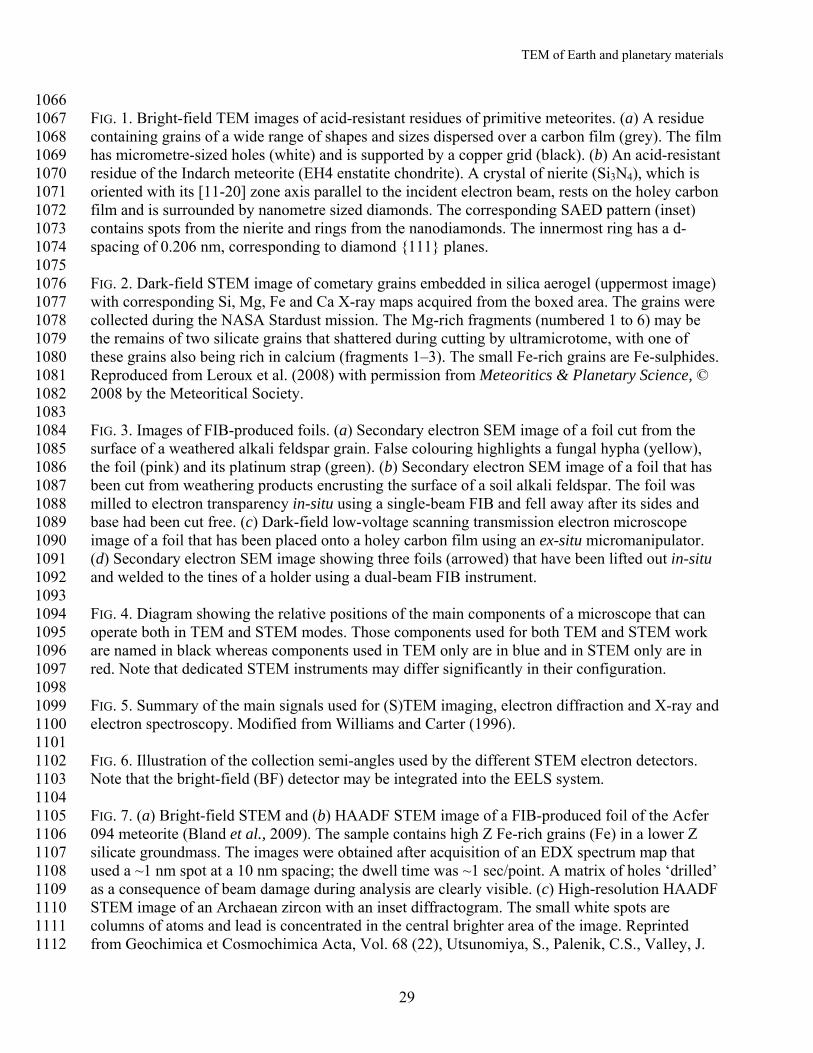
TEM of Earth and planetary materials
29
1066 FIG. 1. Bright-field TEM images of acid-resistant residues of primitive meteorites. (a) A residue 1067 containing grains of a wide range of shapes and sizes dispersed over a carbon film (grey). The film 1068 has micrometre-sized holes (white) and is supported by a copper grid (black). (b) An acid-resistant 1069 residue of the Indarch meteorite (EH4 enstatite chondrite). A crystal of nierite (Si3N4), which is 1070 oriented with its [11-20] zone axis parallel to the incident electron beam, rests on the holey carbon 1071 film and is surrounded by nanometre sized diamonds. The corresponding SAED pattern (inset) 1072 contains spots from the nierite and rings from the nanodiamonds. The innermost ring has a d-1073 spacing of 0.206 nm, corresponding to diamond {111} planes. 1074 1075 FIG. 2. Dark-field STEM image of cometary grains embedded in silica aerogel (uppermost image) 1076 with corresponding Si, Mg, Fe and Ca X-ray maps acquired from the boxed area. The grains were 1077 collected during the NASA Stardust mission. The Mg-rich fragments (numbered 1 to 6) may be 1078 the remains of two silicate grains that shattered during cutting by ultramicrotome, with one of 1079 these grains also being rich in calcium (fragments 1–3). The small Fe-rich grains are Fe-sulphides. 1080 Reproduced from Leroux et al. (2008) with permission from Meteoritics & Planetary Science, © 1081 2008 by the Meteoritical Society. 1082 1083 FIG. 3. Images of FIB-produced foils. (a) Secondary electron SEM image of a foil cut from the 1084 surface of a weathered alkali feldspar grain. False colouring highlights a fungal hypha (yellow), 1085 the foil (pink) and its platinum strap (green). (b) Secondary electron SEM image of a foil that has 1086 been cut from weathering products encrusting the surface of a soil alkali feldspar. The foil was 1087 milled to electron transparency in-situ using a single-beam FIB and fell away after its sides and 1088 base had been cut free. (c) Dark-field low-voltage scanning transmission electron microscope 1089 image of a foil that has been placed onto a holey carbon film using an ex-situ micromanipulator. 1090 (d) Secondary electron SEM image showing three foils (arrowed) that have been lifted out in-situ 1091 and welded to the tines of a holder using a dual-beam FIB instrument. 1092 1093 FIG. 4. Diagram showing the relative positions of the main components of a microscope that can 1094 operate both in TEM and STEM modes. Those components used for both TEM and STEM work 1095 are named in black whereas components used in TEM only are in blue and in STEM only are in 1096 red. Note that dedicated STEM instruments may differ significantly in their configuration. 1097 1098 FIG. 5. Summary of the main signals used for (S)TEM imaging, electron diffraction and X-ray and 1099 electron spectroscopy. Modified from Williams and Carter (1996). 1100 1101 FIG. 6. Illustration of the collection semi-angles used by the different STEM electron detectors. 1102 Note that the bright-field (BF) detector may be integrated into the EELS system. 1103
1104 FIG. 7. (a) Bright-field STEM and (b) HAADF STEM image of a FIB-produced foil of the Acfer 1105 094 meteorite (Bland et al., 2009). The sample contains high Z Fe-rich grains (Fe) in a lower Z 1106 silicate groundmass. The images were obtained after acquisition of an EDX spectrum map that 1107 used a ~1 nm spot at a 10 nm spacing; the dwell time was ~1 sec/point. A matrix of holes ‘drilled’ 1108 as a consequence of beam damage during analysis are clearly visible. (c) High-resolution HAADF 1109 STEM image of an Archaean zircon with an inset diffractogram. The small white spots are 1110 columns of atoms and lead is concentrated in the central brighter area of the image. Reprinted 1111 from Geochimica et Cosmochimica Acta, Vol. 68 (22), Utsunomiya, S., Palenik, C.S., Valley, J. 1112
TEM of Earth and planetary materials
30
W., Cavosie, A.J., Wilde, S.A. and Ewing, R.C., Nanoscale occurrence of Pb in an Archaen 1113 zircon, 4679-4686. Copyright (2004), with permission from Elsevier. 1114 1115 FIG. 8. Bright-field TEM images. (a) An alkali feldspar from the Klokken syenite intrusion 1116 containing a very fine-scale intergrowth of Albite-twinned albite (Aa), Pericline-twinned albite 1117 (Pa) and microcline (M). The foil is oriented with the incident beam parallel to the [001] zone axis 1118 of the Pericline-twinned albite. (b) A detrital alkali feldspar grain from an oil reservoir in the UK 1119 North Sea; the interface between the grain and its K-feldspar overgrowth runs from the NE to SW 1120 corner of the image. In the lower right is microcline of the detrital grain that contains three small 1121 albite exsolution lamellae. Albite and Pericline twins in the microcline are highlighted by bend 1122 contours (B) in the foil. The overgrowth is in the upper left and its mottled appearance is due to a 1123 subgrain microtexture and an abundance of dislocations on subgrain boundaries. 1124 1125 FIG. 9. High resolution TEM image of amphibole from a weathered gedrite gneiss that has been 1126 partially and isovolumetrically transformed to smectite, which fills a SE-NW oriented channel. 1127 Islands of amphibole remain between the smectite and the arrows indicate the smectite reaction 1128 front. Reprinted from Geochimica et Cosmochimica Acta, Vol. 58 (5), Banfield, J.F and Barker, 1129 W.W., Direct observation of reactant-product interfaces formed in natural weathering of exsolved, 1130 defective amphibole to smectite: Evidence for episodic, isovolumetric reactions involving 1131 structural inheritance, 1419-1429. Copyright (1994), with permission from Elsevier. 1132 1133 FIG. 10. High-resolution TEM images of dumortierite-related crystals in an acid-resistant residue 1134 of rose quartz. The images show single fibres viewed down the (a) [112] and (b) [110] directions. 1135 These images are matched with computer simulations of the crystal structure (inset). A 1136 corresponding SAED pattern is also inset to (a). From Ma, C., Goreva, J.S. and Rossman, G.R. 1137 (2002) Fibrous nanoinclusions in massive rose quartz: HRTEM and AEM investigations. 1138 American Mineralogist, 87, 269–276. Reproduced with permission from the Mineralogical Society 1139 of America. 1140 1141 FIG. 11. Electron nanodiffraction (END) patterns of kaolinite. (a) Pattern acquired with the 1142 electron beam oriented parallel to 0.72 nm silicate layers. (b) Pattern acquired with the electron 1143 beam perpendicular to the layers. (c) Pattern showing the effects of radiation damage resulting 1144 from less than 1 second of electron irradiation. Reprinted from Micron, 35 (5), Cowley, J.M., 1145 Applications of electron nanodiffraction, 345-360, Copyright (2004), with permission from 1146 Elsevier. 1147 1148 FIG. 12. Illustrations of the various mechanisms by which a mineral can be damaged during 1149 (S)TEM work. 1150 1151 FIG. 13. Parts of EELS spectra of γ-Mg2SiO4. In [a] the weak Si L2,3 edge is just visible on the 1152 strongly sloping background. [b] is a background-subtracted single spectrum acquired for 2 1153 seconds. [c] has been made from 15 gain-shifted and background-subtracted spectra. The 1154 intensities of [b] and [c] are ten times that of [a]. Reproduced from Garvie, L.A.J. and Buseck, 1155 P.R. (1999) Bonding in silicates: Investigation of the Si L2,3 edge by parallel electron energy-loss 1156 spectroscopy. American Mineralogist, 84, 946–964. With permission from the Mineralogical 1157 Society of America. 1158
TEM of Earth and planetary materials
31
1159 FIG. 14. EELS spectra showing L2,3 edges of elemental Fe and minerals containing single valent 1160 Fe. Reprinted by permission from Macmillan Publishers Ltd: Garvie, L.A.J. and Buseck, P.R. 1161 (1998) Ratios of ferrous to ferric iron from nanometre-sized areas in minerals. Nature 396, 667-1162 670, copyright (1998). 1163 1164 FIG. 15. EFTEM image of desert varnish from the Sonoran Desert, southwestern Arizona (Garvie 1165 et al., 2008). The image is a composite of 20 separate iron (purple) and manganese (green) 1166 EFTEM images acquired from a FIB-produced foil. Most of the black areas of the image are 1167 silica-rich regions. 1168 1169 FIG. 16. Bright-field (a) and dark-field (b) LV-STEM images of kaolinite crystals supported on a 1170 carbon film. (c) Bright-field TEM (upper half) and corresponding dark-field LV-STEM image 1171 (lower half) of a foil cut from the matrix of the Murchison (CM2 carbonaceous chondrite) 1172 meteorite using the FIB technique. The two images are complementary and show that the darker 1173 grains in the bright-field TEM (Fe-rich phyllosilicates, metal and sulphides) correspond to higher 1174 Z grains (light grey) in dark-field LV-STEM. These high-Z grains are enclosed by lower Z Mg-1175 rich phyllosilicates. (d) Dark-field LV-STEM image of the Murchison foil showing Fe-rich 1176 phyllosilicates (Fe-ph) enclosed by very finely crystalline Mg-rich phyllosilicates (Mg-ph) 1177 containing readily resolvable crystals a few tens of nanometres in size. 1178 1179