tunneling transistors for low power electronics
TRANSCRIPT

Tunneling
Transistors for Low
Power Electronics
James Teherani, Tao Yu,
Dimitri Antoniadis, Judy Hoyt
September 16, 2013
Support from
NSF E3S Center
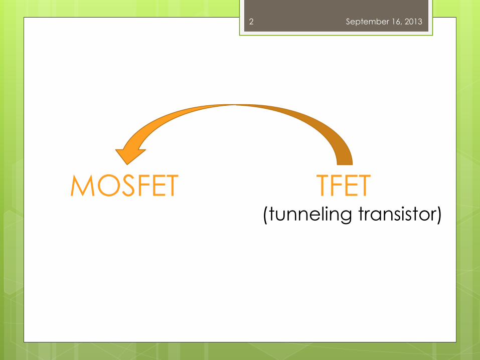
MOSFET TFET
September 16, 20132
(tunneling transistor)

MOSFET Scaling Crisis
September 16, 20133
Frequency scaling stalled
Power density of nuclear reactor
A. Danowitz, K. Kelley, J. Mao, J. P. Stevenson, and M. Horowitz, “CPU DB: Recording Microprocessor History,” Queue, vol. 10, no. 4, pp. 10:10–10:27, 4/2012.
1985 1990 1995 2000 2005 2010 2015
10 GHz
3 GHz
1 GHz
300 MHz
100 MHz
30 MHz
10 MHz
Pro
cesso
r C
lock S
pe
ed
September 16, 20134
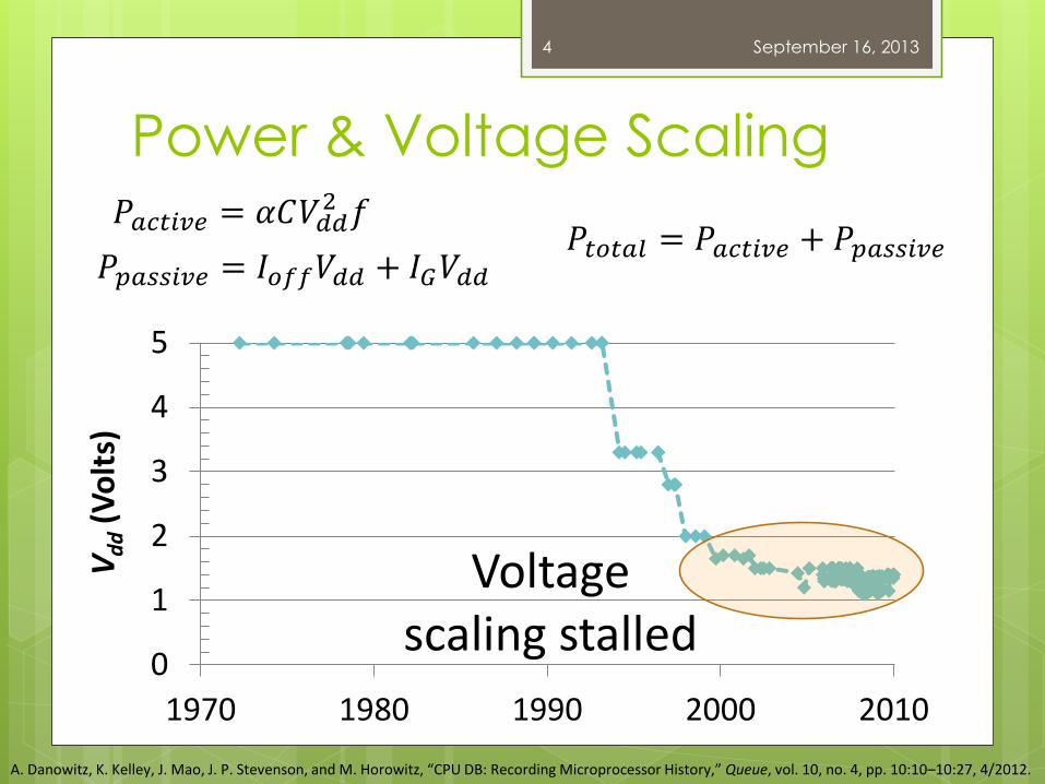
Power & Voltage Scaling𝑃𝑎𝑐𝑡𝑖𝑣𝑒 = 𝛼𝐶𝑉𝑑𝑑
2 𝑓
𝑃𝑝𝑎𝑠𝑠𝑖𝑣𝑒 = 𝐼𝑜𝑓𝑓𝑉𝑑𝑑 + 𝐼𝐺𝑉𝑑𝑑
0
1
2
3
4
5
1970 1980 1990 2000 2010
Vdd
(Vo
lts)
Voltage scaling stalled
𝑃𝑡𝑜𝑡𝑎𝑙 = 𝑃𝑎𝑐𝑡𝑖𝑣𝑒 + 𝑃𝑝𝑎𝑠𝑠𝑖𝑣𝑒
A. Danowitz, K. Kelley, J. Mao, J. P. Stevenson, and M. Horowitz, “CPU DB: Recording Microprocessor History,” Queue, vol. 10, no. 4, pp. 10:10–10:27, 4/2012.
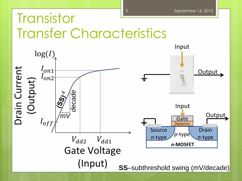
Transfer Characteristics
September 16, 20135
de
ca
de
mV
Dra
in C
urr
ent
(Ou
tpu
t)
Gate Voltage(Input)
𝐼𝑜𝑓𝑓
𝑉𝑑𝑑2 𝑉𝑑𝑑1
𝐼𝑜𝑛2𝐼𝑜𝑛1
Transistor
log(𝐼)
SS–subthreshold swing (mV/decade)
Input
Output
p-type
DielectricGate
n-MOSFET
Input
Output
Sourcen-type
Drainn-type
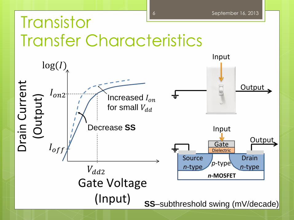
Decrease SS
Transfer Characteristics
September 16, 20136
Dra
in C
urr
ent
(Ou
tpu
t)
Gate Voltage(Input)
𝐼𝑜𝑓𝑓
𝑉𝑑𝑑2
𝐼𝑜𝑛2
Transistor
log(𝐼)
SS–subthreshold swing (mV/decade)
Input
Output
Increased 𝐼𝑜𝑛for small 𝑉𝑑𝑑
p-type
DielectricGate
n-MOSFET
Input
Output
Sourcen-type
Drainn-type
September 16, 20137
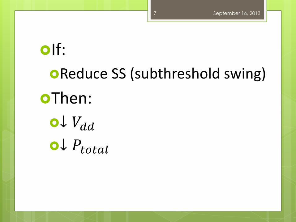
If:
Reduce SS (subthreshold swing)
Then:
↓ 𝑉𝑑𝑑↓ 𝑃𝑡𝑜𝑡𝑎𝑙

SS–Subthreshold Swing (MOSFET)
September 16, 20138
Ener
gy
n-MOSFET
x
Energy distribution of electrons
𝑛 𝐸 = 𝑓(𝐸) ∙ 𝑔𝐷𝑂𝑆(𝐸)thermal tail
CB
VB
Off-state current
𝑓 𝐸 ≈1
exp𝐸 − 𝐸𝑓𝑘𝑇
𝑓 𝐸 ⟹ 60 𝑚𝑉/𝑑𝑒𝑐𝑎𝑑𝑒
Fermi-Dirac Distribution
Source Channel Drain
p-typeDielectric
n-type
Gate
n-typex
𝑓 𝐸1𝑓 𝐸2
≈ exp𝐸2 − 𝐸1𝑘𝑇
Decreased off current
Distribution of Electrons
𝐸2
𝐸1
SS limited to 60 𝑚𝑉/𝑑𝑒𝑐𝑎𝑑𝑒
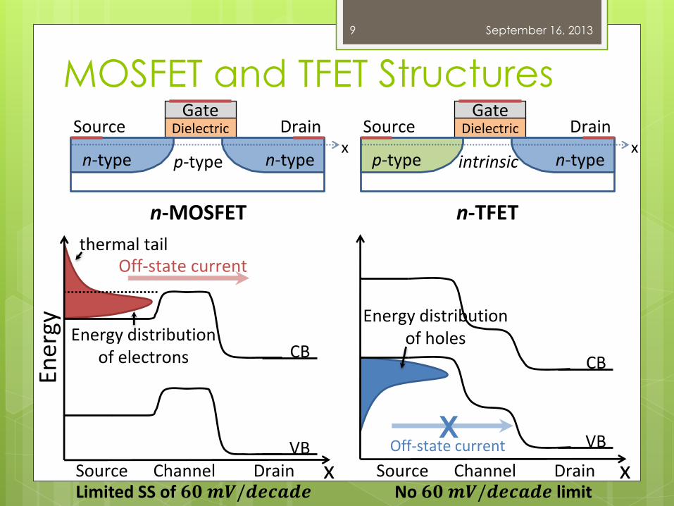
MOSFET and TFET Structures
September 16, 20139
n-TFET
x
Energy distribution of holes
CB
VBOff-state currentX
Ener
gy
n-MOSFET
x
Energy distribution of electrons
thermal tail
CB
VB
Off-state current
Source Channel Drain Source Channel Drain
DielectricSource DrainGate
n-type n-typep-typex
DielectricSource DrainGate
p-type n-typeintrinsicx
Limited SS of 𝟔𝟎𝒎𝑽/𝒅𝒆𝒄𝒂𝒅𝒆 No 𝟔𝟎𝒎𝑽/𝒅𝒆𝒄𝒂𝒅𝒆 limit

Ener
gy
x
CB
VB
DielectricSource DrainGate
p-Si n-Sii-Sin-TFET
x
𝑇 ∝1
exp(𝐴𝑟𝑒𝑎)
Homostructure
September 16, 201310
x
CB
VB
DielectricSource DrainGate
p-GaSb n-InAsi-InAsn-TFET
x
HeterostructureTunneling in
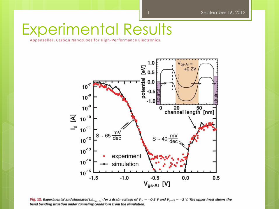
Experimental Results
September 16, 201311
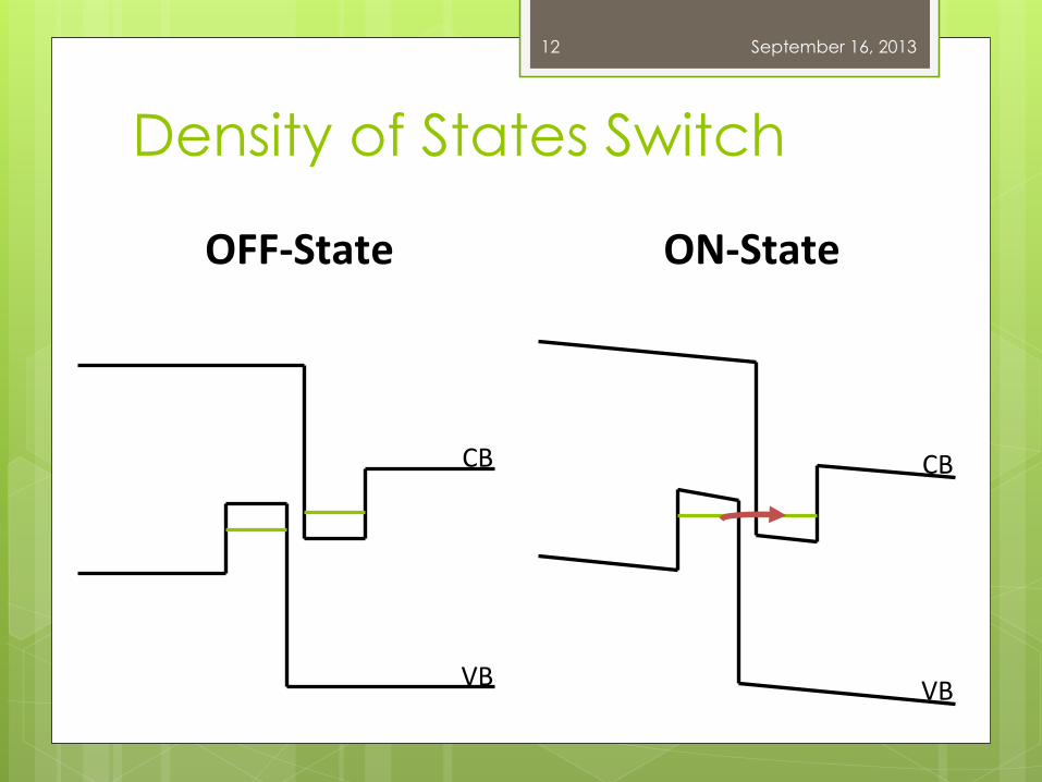
Density of States Switch
September 16, 201312
CB
VB
CB
VB
OFF-State ON-State
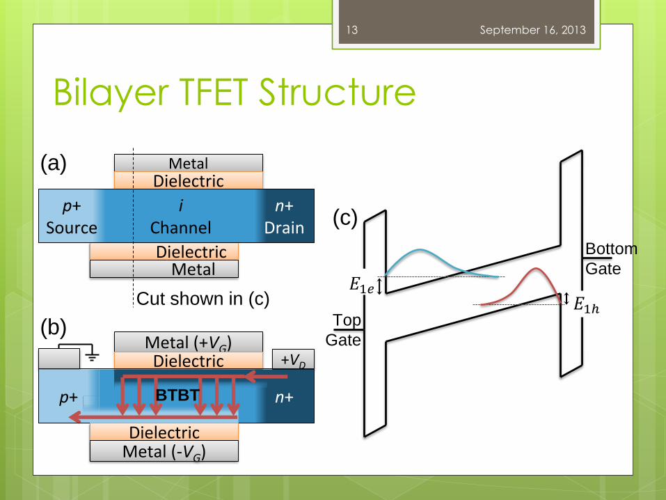
Bilayer TFET Structure
September 16, 201313
+VD
p+ n+
Metal (+VG)Dielectric
(b)
MetalDielectric
(a)
iChannel
p+Source
n+Drain
Cut shown in (c)
DielectricMetal
BTBT
DielectricMetal (-VG)
Bottom
Gate
Top
Gate
(c)
𝐸1ℎ
𝐸1𝑒

Challenges Limiting TFET
Performance
Fundamental
Phonon effects
Band edge abruptness
Technological
Interface states
Complex geometries, design
Junction abruptness
Thickness variation with thin body
structures
Work function engineering
September 16, 201314

Summary
Frequency and voltage scaling of MOSFETs have stalled due to power constraints
Substantial voltage scaling requires new switching physics
TFETs employ tunneling to overcome 60 𝑚𝑉/𝑑𝑒𝑐𝑎𝑑𝑒 limit
Experimental results have shown 𝑺𝑺 < 60 𝑚𝑉/𝑑𝑒𝑐𝑎𝑑𝑒, albeit at low currents
Much work is still needed in matching theory to experiment
Heterojunctions and density-of-states switching designs may lead to better TFET performance
We’re currently exploring the bilayer TFET, which utilizes an interesting device geometry to create electron and hole quantum wells
September 16, 201315