tutorial 1: omni-directional reflectance from a bragg...
TRANSCRIPT
CHAPTER 2 Tutorial 1:Omni-directional reflectance from a Bragg stack using Dmitry Chigrin’s structure.
This tutorial describes how to use one of the pre-defined lattice systems within Translight to explore the omni-directional reflectance properties that can be displayed by Bragg stacks. For this tutorial we use the Bragg stack
used as examined by Dmitry Chigrin1 and compare the results.
Here the theory of omni-directional reflectance for Bragg stacks will not be explained but we will demonstrate how to explore the property using the program. In essence omni-directional reflectance can be achieved due to a limitation in the number of modes that can be excited by externally incident waves on to the stack. The law’s of refraction are well known, Snell’s law, and are applicable when a wave couples from the outside of a Bragg stack to the inside. Given a dielectric boundary interface with an incoming wave with defined incidence angle then the angle of propagation in the second material of the boundary is well known.
Perhaps one of the most important issues concerning omni-directional Bragg stacks is that they require three materials. The number of materials that constitute the stack itself is arbitrary, two materials are normally employed. For omni directional reflectance a third material is required which is the ambient medium. The ambient material need not necessarily be air, it is sufficient that it is different to the other materials. However the ambient medium should have a lower refractive index than the other materials. This condition imposes the angle coupling limitation through Snell’s law. For a more rigorous approach to omni-directional reflectance, see Chigrin’s paper1.
1. All dielectric One-Dimensional Periodic Structures for Total Omnidirectional Reflection and Par-tial Spontaneous Emission Control, D.N. Chigrin, A.V. Lavrinenko, D.A. Yarotsky, and S.V. Gapo-nenko, Journal of Lightwave Technology, Vol 17, No 11., November 1999.
35

Tutorial 1: Omni-directional reflectance from a Bragg stack using Dmitry Chigrin’s structure.
2.1: Selecting Chigrin’s Stack
Start the program and select the structure tab at the top of the graphical interface. Depending on whether or not a pre-defined system is already in use the ‘Use Predefined System’ check box be checked, i.e. it has a small tick symbol in the box. If there is no tick, click once on the box, the tick should appear and the drop down box on the right should activate by turning from grey to white.
To select Chigrin’s bragg stack in dielectric simply click on the drop down arrow, located on the right of the selection bar. Once clicked a list of all the pre-defined systems will appear. As there are several predefined systems, more than can be displayed in the drop down window available, a scroll bar will also appear. Click and drag this scroll bar until the words ‘Chigrin’s Bragg Stack in Dielectric’ become visible. Once visible use the mouse to select this option as is shown in Figure 2.1. Once selected you should see that the parameters on the screen change to reflect those that are shown in Figure 2.1.
Mesh to Represent Structure.
Note that as a Bragg stack is a one dimensional structure that the mesh that we use to represent the structure also need only be one dimensional. You can see the mesh that is used to represent the structure in the group box labelled ‘Mesh to Represent Structure’. The sub mesh is the number of points that are used between the larger sampling mesh points to obtain an accurate average for the point. The check box, ‘Construct Cell Only’ will force the program to build the cell under study and then stop without performing the transmission / reflection analysis. This feature is useful to check that the structure intended for study has been defined correctly both in VRML, and within the file gnet.dat located in the Crystal subdirectory. The gnet.dat file lists the x,y and z coordinates within the cell against the complex dielectric constant.
Figure 2.1 Selecting Chigrin’s Bragg Stack
Photonic Band Gap Materials Research Group, Department of Electronics & Electrical Engineering, The University of Glasgow, Rankine Building G12 8LT
Tel.+44(0)141-330-6022 Fax.+44(0)141-330-6002: Email:[email protected]

Selecting Chigrin’s Stack
Structure Features.
For the Bragg stack selected the selected feature will move to that of a ‘Bar’. As the Bragg stack is one dimensional the ‘Bar’ is the only shape that is relevant as spheres and cylinders require further dimensions to be represented properly.
Cell Repetitions.
The boxes listed under this heading expand the number of crystal periods expressed in the VRML file and within the gnet.dat file. DO NOT confuse this with the number of crystal periods under study within the analysis aspect of the code. The cell repetition aspect is provided so that a bulk piece of crystal can be build, this allows the geometry to be explored and can provide impressive results within VRML.
The check box ‘Chunk’ ensures that if multiple cells are used then one large cell is created in the gnet.dat file. The program ensures that the cells are joined together in the correct way. If ‘Chunk’ is not selected then the individual cells will be written to the gnet.dat file sequentially. Note that at this time that the joining together of multiple cells does not respect the intended repetition of each individual cell. This statement is best explained through use of an example; for a planar cavity we may utilise three cells to build the structure in Table 1.
Evidently ‘Cell 1’ is repeated five times before the cavity is encountered and ‘Cell 3’ is repeated five times after the cavity. With the ‘Chunk’ box checked on and the repetition factors set such that X=4, Y=1 and Z=1 then the output in both the VRML file and the gnet.dat file is shown in Table 2.
The cell has been expanded 4 times in the x-direction as selected by the repetition parameters. As we are using more than one cell changing the Z magnification value will have no effect as repeating the structure in the z-dimension complicated. Altering the Y repetition factor will increase the length of the cylinders in VRML but do little else as in this 2D instance the Y plane is the translational invariant plane. For visualisation purposes there is a work around to this which involves using more cells. Transmission analysis can also be done but will give the same transmission results and take far longer. To generate the correct visual structure for the wanted crystal we would need to use 11 cells to build the structure.
Structure Cellso o o o o o o o o o 1 2 3o o o o o o o o o o o oo o o o o o o o o o o o o o o o o o o o
TABLE 1 :Example of a simple planar cavity crystal.
1 2 3o oo oo oo o
TABLE 2 :Resultant Output
Photonic Band Gap Materials Research Group, Department of Electronics & Electrical Engineering, The University of Glasgow, Rankine Building G12 8LT
Tel.+44(0)141-330-6022 Fax.+44(0)141-330-6002: Email:[email protected] 37
Tutorial 1: Omni-directional reflectance from a Bragg stack using Dmitry Chigrin’s structure.
Lattice Constant / Cell Size.
The lattice constant is listed in the program so that actual structures can be studied. When no losses are present and refractive indices are assumed to be constant then band structure results and transmission spectra can be scaled. When dielectric losses are introduced or frequency dependent refractive indices then the actual crystal becomes important, therefore the user can define a lattice constant. Care should be exercised when altering the lattice constant such that the discretization mesh respects Nyquist’s law. This means that for the frequency of interest a good representation of the wave form within the materials should be obtained.
The cell sizes are normalised to the lattice constant, they are not expressed in metres or direct spatial units. For a cubic lattice the X, Y and Z-Cell sizes will all be the same and set to unity. For Chigrin’s Bragg stack the X, Y and Z-Cell size are also all unity, the code internally makes the correct adjustments to deal with the fact that we are only working in one dimension.
VRML Output.
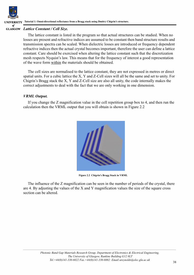
If you change the Z magnification value in the cell repetition group box to 4, and then run the calculation then the VRML output that you will obtain is shown in Figure 2.2
The influence of the Z magnification can be seen in the number of periods of the crystal, there are 4. By adjusting the values of the X and Y magnification values the size of the square cross section can be altered.
Figure 2.2 Chigrin’s Bragg Stack in VRML
Photonic Band Gap Materials Research Group, Department of Electronics & Electrical Engineering, The University of Glasgow, Rankine Building G12 8LT
Tel.+44(0)141-330-6022 Fax.+44(0)141-330-6002: Email:[email protected]
Setting up the materials and feature properties.
2.2: Setting up the materials and feature properties.
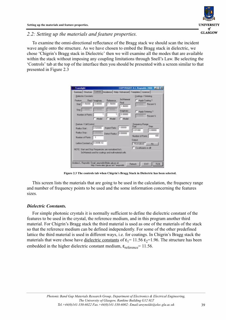
To examine the omni-directional reflectance of the Bragg stack we should scan the incident wave angle onto the structure. As we have chosen to embed the Bragg stack in dielectric, we chose ‘Chigrin’s Bragg stack in Dielectric’ then we will examine all the modes that are available within the stack without imposing any coupling limitations through Snell’s Law. Be selecting the ‘Controls’ tab at the top of the interface then you should be presented with a screen similar to that presented in Figure 2.3
This screen lists the materials that are going to be used in the calculation, the frequency range and number of frequency points to be used and the some information concerning the features sizes.
Dielectric Constants.
For simple photonic crystals it is normally sufficient to define the dielectric constant of the features to be used in the crystal, the reference medium, and in this program another third material. For Chigrin’s Bragg stack the third material is used as one of the materials of the stack so that the reference medium can be defined independently. For some of the other predefined lattice the third material is used in different ways, i.e. for coatings. In Chigrin’s Bragg stack the materials that were chose have dielectric constants of ε1= 11.56 ε2=1.96. The structure has been embedded in the higher dielectric constant medium, εreference= 11.56.
Figure 2.3 The controls tab when Chigrin’s Bragg Stack in Dielectric has been selected.
Photonic Band Gap Materials Research Group, Department of Electronics & Electrical Engineering, The University of Glasgow, Rankine Building G12 8LT
Tel.+44(0)141-330-6022 Fax.+44(0)141-330-6002: Email:[email protected] 39

Tutorial 1: Omni-directional reflectance from a Bragg stack using Dmitry Chigrin’s structure.
Frequency Range.
The start and stop frequencies of the calculation can be selected and altered along with the number of frequency points. Both the start and stop frequencies are expressed in normalised units which is related to the lattice constant through the Equation 2.1
Under the frequency start and stop edit boxes there are two push button boxes labelled ‘Normalised’ and ‘Hertz’, and a check box labelled ‘Coefficients dB’. These boxes relate to the output that will be generated in analysis of the program. If the Hertz box is pushed then the output files will relate the transmission and reflection coefficients to frequency expressed in Hertz, similarly if the Normalised button is selected then the files will be expressed in normalised frequency. The check box ‘Coefficients dB’ will change the coefficients from a linear scale to a logarithmic scale if checked. Set the start frequency to 0.01, the stop to 0.8 and choose 400 frequency points.
Feature / Cell Control.
Within this group control of the features can be achieved and loops can be introduced if required. The radius start and stop values are again normalised to the lattice constant such that the values displayed are r/a where r=radius and a=lattice constant. For Chigrin’s Bragg Stack the ‘Radius Start’ value is set to 0.5, this signifies the proportion of the one dimensional cell that is occupied by the feature material. For Chigrin’s Bragg stack the thickness of the ε1= 11.56 ε2=1.96 materials is equal, if the thickness of each layer is denoted as t, then t1/t2=1 and t1+t2=a. Consequently r/a=0.5 where r=t1.
The ‘Aspect’ control and defect radius are not used in with Chigrin’s Bragg stack, explanation is covered elsewhere. The lattice constant value is also shown within the Feature / Cell Control box. Many of the menus have parameters repeated between them, changing the value in one menu will alter the values across all of the menu.
Coating / Sintering.
These parameters are used in conjunction with Opal photonic crystals and therefore do not merit discussion here.
Equation 2.1 Normalised Frequency
Normalised FrequencyFrequency (Hz) x Lattice Constant (m)
Speed of Light(ms-1)---------------------------------------------------------------------------------------------=
Photonic Band Gap Materials Research Group, Department of Electronics & Electrical Engineering, The University of Glasgow, Rankine Building G12 8LT
Tel.+44(0)141-330-6022 Fax.+44(0)141-330-6002: Email:[email protected]

Normal Incidence Calculation.
2.3: Normal Incidence Calculation.
At this point we can already run a simple calculation on our structure. Assuming that the incidence vector controls are both set to zero, Kx=0, Ky=0 in the incidence tab menu and that you have altered the start and stop frequency, simply press the refresh button once, and the run the calculation.
For normal incidence on to a Bragg stack the TE and TM polarised waves have the same transmission and reflection response. The pre-defined system perform the transmission and reflection characterisation for Chigrin’s stack with eight periods of crystal in the propagation direction. The coefficients for both TE and TM polarised waves, for reflection and for transmission are found in the ‘Coeff’ subdirectory which will be created in the same directory folder as the main executable Translight. The transmission and reflection spectra are shown plotted against normalised frequency in Figure 2.4
From point of principal we note here that the transmission and reflection spectra are calculated independently. For loss less systems reflection plus transmission should always add together to give a value of unity, i.e. R+T=1. For systems that include losses then the R+T=1 formula also incorporates a further element, absorption; R+T+A=1.
To investigate the omni directional behaviour of the stack we now must scan the incidence angle of the incoming wave onto the structure. From this analysis we will be able to ascertain whether the structure has an omni-directional gap, see “Controlling / Scanning the Incidence Angle.” on page 42.
Figure 2.4 Normal Incidence Response
Photonic Band Gap Materials Research Group, Department of Electronics & Electrical Engineering, The University of Glasgow, Rankine Building G12 8LT
Tel.+44(0)141-330-6022 Fax.+44(0)141-330-6002: Email:[email protected] 41
Tutorial 1: Omni-directional reflectance from a Bragg stack using Dmitry Chigrin’s structure.
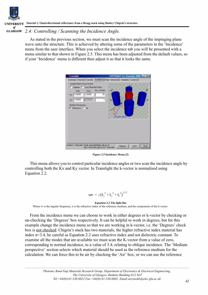
2.4: Controlling / Scanning the Incidence Angle.
As stated in the previous section, we must scan the incidence angle of the impinging plane wave onto the structure. This is achieved by altering some of the parameters in the ‘Incidence’ menu from the user interface. When you select the incidence tab you will be presented with a menu similar to that shown in Figure 2.5. This menu has been adjusted from the default values, so if your ‘Incidence’ menu is different then adjust it so that it looks the same.
This menu allows you to control particular incidence angles or two scan the incidence angle by controlling both the Kx and Ky vector. In Translight the k-vector is normalised using Equation 2.2.
From the incidence menu we can choose to work in either degrees or k-vector by checking or un-checking the ‘Degrees’ box respectively. It can be helpful to work in degrees, but for this example change the incidence menu so that we are working in k-vector, i.e. the ‘Degrees’ check box is not checked. Chigrin’s stack has two materials, the higher refractive index material has index n=3.4, be careful as Equation 2.2 uses refractive index and not dielectric constant. To examine all the modes that are available we must scan the K-vector from a value of zero, corresponding to normal incidence, to a value of 3.4, relating to oblique incidence. The ‘Medium perspective’ section selects which material should be used as the reference medium for the calculation. We can force this to be air by checking the ‘Air’ box, or we can use the reference
Figure 2.5 Incidence Menu (2)
Equation 2.2 The light lineWhere w is the angular frequency, n is the refractive index of the reference medium, and the components of the k-vector.
ωn c kx2 ky
2 kz2+ +( )
1 2⁄=
Photonic Band Gap Materials Research Group, Department of Electronics & Electrical Engineering, The University of Glasgow, Rankine Building G12 8LT
Tel.+44(0)141-330-6022 Fax.+44(0)141-330-6002: Email:[email protected]
Controlling / Scanning the Incidence Angle.
medium value which we set in the ‘Controls’ tab, (see “Setting up the materials and feature properties.” on page 39). In this instance we will use the reference medium.
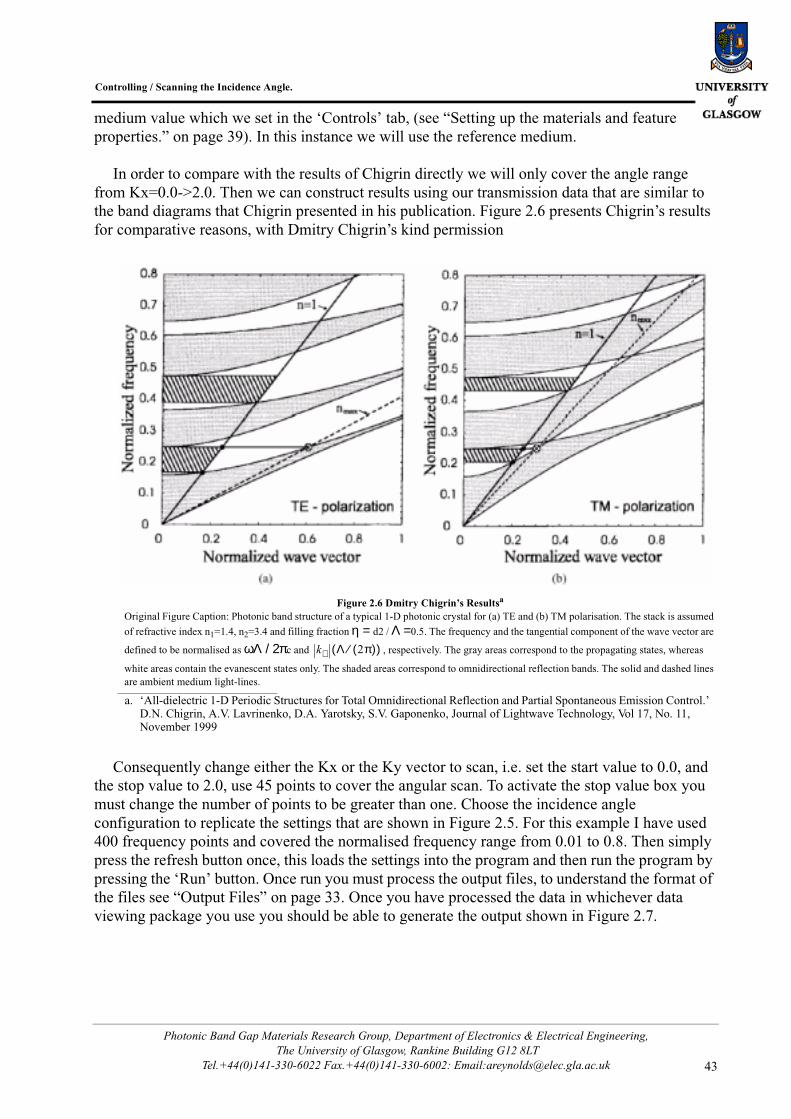
In order to compare with the results of Chigrin directly we will only cover the angle range from Kx=0.0->2.0. Then we can construct results using our transmission data that are similar to the band diagrams that Chigrin presented in his publication. Figure 2.6 presents Chigrin’s results for comparative reasons, with Dmitry Chigrin’s kind permission
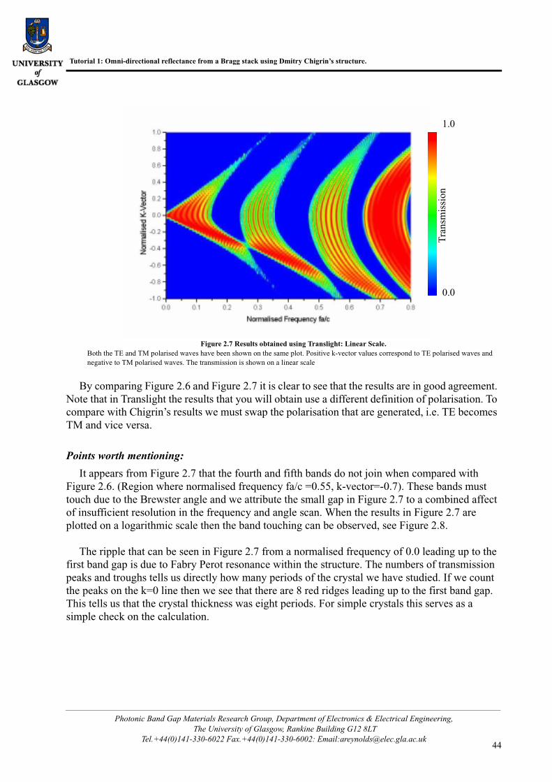
Consequently change either the Kx or the Ky vector to scan, i.e. set the start value to 0.0, and the stop value to 2.0, use 45 points to cover the angular scan. To activate the stop value box you must change the number of points to be greater than one. Choose the incidence angle configuration to replicate the settings that are shown in Figure 2.5. For this example I have used 400 frequency points and covered the normalised frequency range from 0.01 to 0.8. Then simply press the refresh button once, this loads the settings into the program and then run the program by pressing the ‘Run’ button. Once run you must process the output files, to understand the format of the files see “Output Files” on page 33. Once you have processed the data in whichever data viewing package you use you should be able to generate the output shown in Figure 2.7.
Figure 2.6 Dmitry Chigrin’s Resultsa
Original Figure Caption: Photonic band structure of a typical 1-D photonic crystal for (a) TE and (b) TM polarisation. The stack is assumed
of refractive index n1=1.4, n2=3.4 and filling fraction η = d2 / Λ =0.5. The frequency and the tangential component of the wave vector are
defined to be normalised as ωΛ / 2πc and , respectively. The gray areas correspond to the propagating states, whereas
white areas contain the evanescent states only. The shaded areas correspond to omnidirectional reflection bands. The solid and dashed lines are ambient medium light-lines.
a. ‘All-dielectric 1-D Periodic Structures for Total Omnidirectional Reflection and Partial Spontaneous Emission Control.’ D.N. Chigrin, A.V. Lavrinenko, D.A. Yarotsky, S.V. Gaponenko, Journal of Lightwave Technology, Vol 17, No. 11, November 1999
k⊥ Λ 2π( )⁄( )
Photonic Band Gap Materials Research Group, Department of Electronics & Electrical Engineering, The University of Glasgow, Rankine Building G12 8LT
Tel.+44(0)141-330-6022 Fax.+44(0)141-330-6002: Email:[email protected] 43
Tutorial 1: Omni-directional reflectance from a Bragg stack using Dmitry Chigrin’s structure.
By comparing Figure 2.6 and Figure 2.7 it is clear to see that the results are in good agreement. Note that in Translight the results that you will obtain use a different definition of polarisation. To compare with Chigrin’s results we must swap the polarisation that are generated, i.e. TE becomes TM and vice versa.
Points worth mentioning:
It appears from Figure 2.7 that the fourth and fifth bands do not join when compared with Figure 2.6. (Region where normalised frequency fa/c =0.55, k-vector=-0.7). These bands must touch due to the Brewster angle and we attribute the small gap in Figure 2.7 to a combined affect of insufficient resolution in the frequency and angle scan. When the results in Figure 2.7 are plotted on a logarithmic scale then the band touching can be observed, see Figure 2.8.
The ripple that can be seen in Figure 2.7 from a normalised frequency of 0.0 leading up to the first band gap is due to Fabry Perot resonance within the structure. The numbers of transmission peaks and troughs tells us directly how many periods of the crystal we have studied. If we count the peaks on the k=0 line then we see that there are 8 red ridges leading up to the first band gap. This tells us that the crystal thickness was eight periods. For simple crystals this serves as a simple check on the calculation.
Figure 2.7 Results obtained using Translight: Linear Scale.Both the TE and TM polarised waves have been shown on the same plot. Positive k-vector values correspond to TE polarised waves and negative to TM polarised waves. The transmission is shown on a linear scale
Tra
nsm
issi
on
1.0
0.0
Photonic Band Gap Materials Research Group, Department of Electronics & Electrical Engineering, The University of Glasgow, Rankine Building G12 8LT
Tel.+44(0)141-330-6022 Fax.+44(0)141-330-6002: Email:[email protected]

Controlling / Scanning the Incidence Angle.
Interim conclusion.
In summary we have performed the transmission analysis that Chigrin presented in terms of band diagrams. From this information, Figure 2.6, Figure 2.7 and Figure 2.8 we have seen that for any given normalised frequency, without applying any conditions or assumptions, that there is not a region where we have close to zero transmission for all values of the k-vector. However, when we limit the k-vector in value by changing the ambient medium in from which the stack is excited then we can achieve omni-directional reflectance. Next we must change the stack to be in air......
Figure 2.8 Results obtained using Translight: Logarithmic Scale.Both the TE and TM polarised waves have been shown on the same plot. Positive k-vector values correspond to TE polarised waves and negative to TM polarised waves. The transmission is shown on a logarithmic scale. Values below -100dB are shown in white.
Tra
nsm
issi
on
-100db
0.0db
Photonic Band Gap Materials Research Group, Department of Electronics & Electrical Engineering, The University of Glasgow, Rankine Building G12 8LT
Tel.+44(0)141-330-6022 Fax.+44(0)141-330-6002: Email:[email protected] 45
Tutorial 1: Omni-directional reflectance from a Bragg stack using Dmitry Chigrin’s structure.
2.5: Examining the Bragg stack embedded in air.
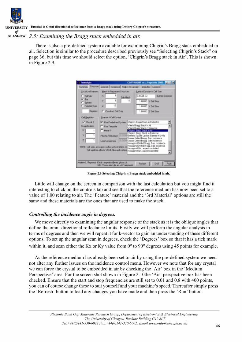
There is also a pre-defined system available for examining Chigrin’s Bragg stack embedded in air. Selection is similar to the procedure described previously see “Selecting Chigrin’s Stack” on page 36, but this time we should select the option, ‘Chigrin’s Bragg stack in Air’. This is shown in Figure 2.9.
Little will change on the screen in comparison with the last calculation but you might find it interesting to click on the controls tab and see that the reference medium has now been set to a value of 1.00 relating to air. The ‘Feature’ material and the ‘3rd Material’ options are still the same and these materials are the ones that are used to make the stack.
Controlling the incidence angle in degrees.
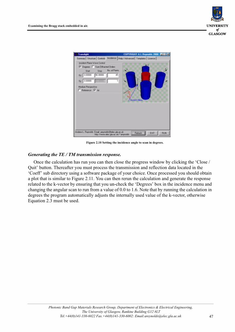
We move directly to examining the angular response of the stack as it is the oblique angles that define the omni-directional reflectance limits. Firstly we will perform the angular analysis in terms of degrees and then we will repeat it for k-vector to gain an understanding of these different options. To set up the angular scan in degrees, check the ‘Degrees’ box so that it has a tick mark
within it, and scan either the Kx or Ky value from 0o to 90o degrees using 45 points for example.
As the reference medium has already been set to air by using the pre-defined system we need not alter any further issues on the incidence control menu. However we note that for any crystal we can force the crystal to be embedded in air by checking the ‘Air’ box in the ‘Medium Perspective’ area. For the screen shot shown in Figure 2.10the ‘Air’ perspective box has been checked. Ensure that the start and stop frequencies are still set to 0.01 and 0.8 with 400 points, you can of course change these to suit yourself and your machine’s speed. Thereafter simply press the ‘Refresh’ button to load any changes you have made and then press the ‘Run’ button.
Figure 2.9 Selecting Chigrin’s Bragg stack embedded in air.
Photonic Band Gap Materials Research Group, Department of Electronics & Electrical Engineering, The University of Glasgow, Rankine Building G12 8LT
Tel.+44(0)141-330-6022 Fax.+44(0)141-330-6002: Email:[email protected]
Examining the Bragg stack embedded in air.
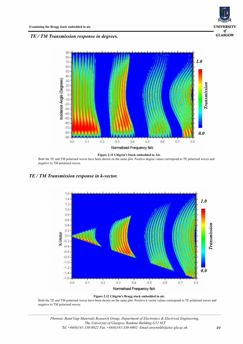
Generating the TE / TM transmission response.
Once the calculation has run you can then close the progress window by clicking the ‘Close / Quit’ button. Thereafter you must process the transmission and reflection data located in the ‘Coeff’ sub directory using a software package of your choice. Once processed you should obtain a plot that is similar to Figure 2.11. You can then rerun the calculation and generate the response related to the k-vector by ensuring that you un-check the ‘Degrees’ box in the incidence menu and changing the angular scan to run from a value of 0.0 to 1.6. Note that by running the calculation in degrees the program automatically adjusts the internally used value of the k-vector, otherwise Equation 2.3 must be used.
Figure 2.10 Setting the incidence angle to scan in degrees.
Photonic Band Gap Materials Research Group, Department of Electronics & Electrical Engineering, The University of Glasgow, Rankine Building G12 8LT
Tel.+44(0)141-330-6022 Fax.+44(0)141-330-6002: Email:[email protected] 47
Tutorial 1: Omni-directional reflectance from a Bragg stack using Dmitry Chigrin’s structure.
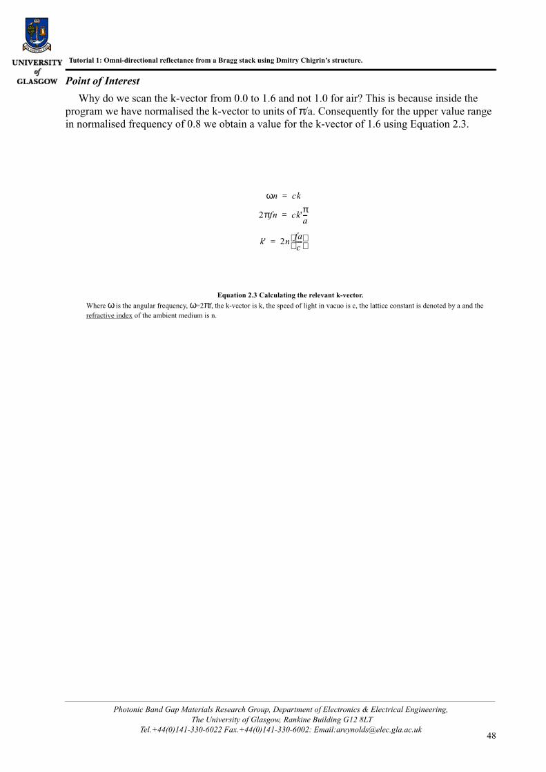
Point of Interest
Why do we scan the k-vector from 0.0 to 1.6 and not 1.0 for air? This is because inside the program we have normalised the k-vector to units of π/a. Consequently for the upper value range in normalised frequency of 0.8 we obtain a value for the k-vector of 1.6 using Equation 2.3.
Equation 2.3 Calculating the relevant k-vector.
Where ω is the angular frequency, ω=2πf, the k-vector is k, the speed of light in vacuo is c, the lattice constant is denoted by a and the refractive index of the ambient medium is n.
ωn ck=
2πfn ck'πa---=
k' 2nfac-----
=
Photonic Band Gap Materials Research Group, Department of Electronics & Electrical Engineering, The University of Glasgow, Rankine Building G12 8LT
Tel.+44(0)141-330-6022 Fax.+44(0)141-330-6002: Email:[email protected]
Examining the Bragg stack embedded in air.
TE / TM Transmission response in degrees.
TE / TM Transmission response in k-vector.
Figure 2.11 Chigrin’s Stack embedded in Air.Both the TE and TM polarised waves have been shown on the same plot. Positive degree values correspond to TE polarised waves and negative to TM polarised waves.
Figure 2.12 Chigrin’s Bragg stack embedded in air.Both the TE and TM polarised waves have been shown on the same plot. Positive k vector values correspond to TE polarised waves and negative to TM polarised waves.
1.0
0.0
Tra
nsm
issi
on1.0
0.0
Tra
nsm
issi
on
Photonic Band Gap Materials Research Group, Department of Electronics & Electrical Engineering, The University of Glasgow, Rankine Building G12 8LT
Tel.+44(0)141-330-6022 Fax.+44(0)141-330-6002: Email:[email protected] 49

Tutorial 1: Omni-directional reflectance from a Bragg stack using Dmitry Chigrin’s structure.
2.6: Defining your own Bragg stack.
There are two ways to define your own Bragg stack, we will explore one method here using templates. The template files are stored in the ‘/Template’ sub-directory located in the same directory as the main Translight executable. The files in this directory are used in conjunction with the ‘Control.dat’ file to build crystals that you can define. You are able to control the materials, the cell sizes, the type of features that are used to build the lattice and many other aspects of the lattice. All the other controls relating to the analysis remain with the GUI, to use templates you must use the GUI.
The first step in generating a template file is to pick a crystal that is close to your needs. As we started using ‘Chigrin’s Bragg stack in Dielectric’ return to the ‘Structure’ menu and pick this pre-defined system once again, as shown in Figure 2.13.
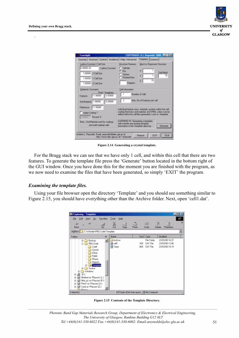
By choosing this system we load the program with the parameter required to build the stack including the lattice information. Now we need to output this lattice information so that we can alter it. To do this we should select the ‘Templates’ tab, Figure 2.14.
This menu screen overviews the current settings used for the crystal that is presently loaded. If you are not using a pre-defined system then you can change many of the on screen parameters to suit your needs. You will however be unable to adjust the total number of cells and the maximum number of features per cell, these values relate to how the crystal is built and refer to internal memory definitions within the code, therefore you cannot change them. Do not let this aspect worry you here after we are free to alter the template files in which ever means we wish. We can add more cells and more features until we can build the crystal we want. In essence we are only using the code to generate a skeleton of the crystal that we wish to study.
Figure 2.13 Selecting Chigrin’s Bragg Stack in Dielectric.
Photonic Band Gap Materials Research Group, Department of Electronics & Electrical Engineering, The University of Glasgow, Rankine Building G12 8LT
Tel.+44(0)141-330-6022 Fax.+44(0)141-330-6002: Email:[email protected]
Defining your own Bragg stack.
.
For the Bragg stack we can see that we have only 1 cell, and within this cell that there are two features. To generate the template file press the ‘Generate’ button located in the bottom right of the GUI window. Once you have done this for the moment you are finished with the program, as we now need to examine the files that have been generated, so simply ‘EXIT’ the program.
Examining the template files.
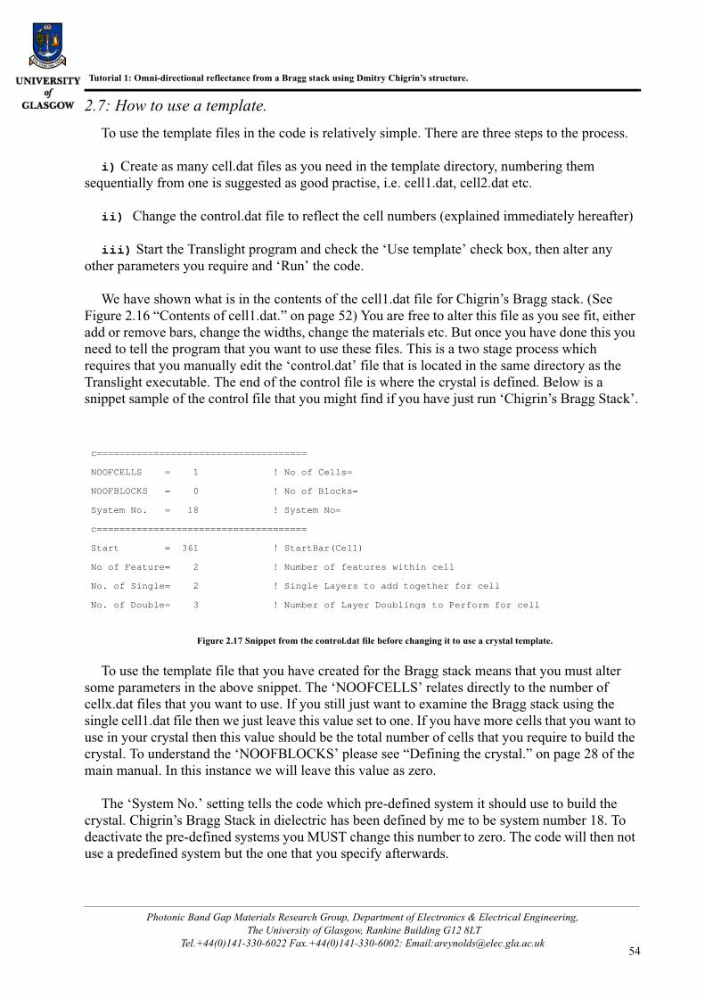
Using your file browser open the directory ‘Template’ and you should see something similar to Figure 2.15, you should have everything other than the Archive folder. Next, open ‘cell1.dat’.
Figure 2.14 Generating a crystal template.
Figure 2.15 Contents of the Template Directory.
Photonic Band Gap Materials Research Group, Department of Electronics & Electrical Engineering, The University of Glasgow, Rankine Building G12 8LT
Tel.+44(0)141-330-6022 Fax.+44(0)141-330-6002: Email:[email protected] 51

Tutorial 1: Omni-directional reflectance from a Bragg stack using Dmitry Chigrin’s structure.
When you have opened cell1.dat and maximised the screen the contents of the file should look like the file listed Figure 2.16. Note that layout of this file is sensitive so when editing it do not alter the format of the file as otherwise the code will not be able to read it properly
Starting from the top of the file we can see that we have defined the discretisation mesh that will represent this cell, and the next row overviews the dimensions of this cell. Note that for a Bragg stack the X and Y dimensions have been valued at 0.3E-2, these values are not actually used by the code as it will interpret from the discretisation mesh that the structure is only 1-dimensional.
Next we encounter the line ‘Build crystal using’, this tells the code that this crystal will be built using either, bars (b), cylinders (c), or spheres (s). Note that currently you cannot mix different types in one crystal, the crystal must be made entirely from one ‘type’.
The lattice spacing is expressed in metres. For some of the crystals it may not be necessary to define a lattice spacing. Furthermore it might not be intuitive for a particular lattice, such an example is the woodpile which has an FCT geometry. What is important is that the output in the files can be in normalised frequency, and the normalisation will be carried out using this lattice constant value.(see “Frequency Range.” on page 40).
As we are defining a Bragg stack we require that there are two ‘Bars’ in the cell. In this instance each bar has the same thickness but is made from a different material. You can see the bar number, and the fact that the features are b (bars) on the left of the file. These two values are read by the program but not used, so don’t worry that the numbers are consecutive. After the feature identifier information we see the real and imaginary part of the material that is used to make the bar. Next we encounter the position of the bar within the cell. Note that the position is in relation to a normalised cell, therefore to place a feature in the middle of a cell, (0.5,0.5,0.5) would be used as the (x,y,z) origin value regardless of the cell dimensions. The origin of each shape is found in its centre. At first glance this maybe seem counter intuitive but it is a powerful aspect of the code which we will discuss later.
Figure 2.16 Contents of cell1.dat.
|----Description--|-----X-----|-----Y-----|-----Z----|Discretisation Mesh 1 1 15Cell Dimensions (m) 0.3000E-02 0.3000E-02 0.3000E-02Build Crystal Using: bLattice Constant :0.3000E-02--------------------------------FEATURES------------------------------------*No.*|***Material****|**Origins Matrix**|AXIS|********Bar Width*******|**VRML**|*Type¦--Real--¦ Imag-|--X---|--Y---|--Z---|--|---X---¦---Y---¦---Z----|-Colour- 1 b 11.560 0.000 0.500 0.000 0.250 y 1.00000 1.00000 0.50000 white 2 b 1.960 0.000 0.500 0.000 0.750 y 1.00000 1.00000 0.50000 blue
Photonic Band Gap Materials Research Group, Department of Electronics & Electrical Engineering, The University of Glasgow, Rankine Building G12 8LT
Tel.+44(0)141-330-6022 Fax.+44(0)141-330-6002: Email:[email protected]

Defining your own Bragg stack.
After the definition of the position of the bars we encounter the orientation axis. This is an important issue for 2 and 3 dimensional structures. This is covered in the next section, see “Template File Differences.” on page 58.
Next we can read the dimensions of each bar expressed again in units normalised to the unit cell lengths in x,y and z. You can see that the bar dimensions in the z-dimension are both set to 0.5, this means that one bar takes up half of the cell, the other taking the other half. To regress slightly we can see from the origins matrix for each bar that the bars have been placed at z=0.25, and z=0.75. This makes perfect sense because the bars are both 0.5*zcell wide. To correctly place the bars in the cell then we recall that we should define the point where the centre of the bar should be placed. For the first bar, the centre is placed at z=0.25, then the bar spans the z region from 0->0.5, the middle being 0.25. For the second bar the centre should be placed at z=0.75, and it will then span the region z=0.5->1.0. Thus, we have filled the cell correctly. If there are gaps in the cell that you define then they will be filled with the reference material that you can define.
Finally we see the colour that is used to define the bar in VRML, the colours that are presently available are, black, white, green, blue and red.
Photonic Band Gap Materials Research Group, Department of Electronics & Electrical Engineering, The University of Glasgow, Rankine Building G12 8LT
Tel.+44(0)141-330-6022 Fax.+44(0)141-330-6002: Email:[email protected] 53
Tutorial 1: Omni-directional reflectance from a Bragg stack using Dmitry Chigrin’s structure.
2.7: How to use a template.
To use the template files in the code is relatively simple. There are three steps to the process.
i) Create as many cell.dat files as you need in the template directory, numbering them sequentially from one is suggested as good practise, i.e. cell1.dat, cell2.dat etc.
ii) Change the control.dat file to reflect the cell numbers (explained immediately hereafter)
iii) Start the Translight program and check the ‘Use template’ check box, then alter any other parameters you require and ‘Run’ the code.
We have shown what is in the contents of the cell1.dat file for Chigrin’s Bragg stack. (See Figure 2.16 “Contents of cell1.dat.” on page 52) You are free to alter this file as you see fit, either add or remove bars, change the widths, change the materials etc. But once you have done this you need to tell the program that you want to use these files. This is a two stage process which requires that you manually edit the ‘control.dat’ file that is located in the same directory as the Translight executable. The end of the control file is where the crystal is defined. Below is a snippet sample of the control file that you might find if you have just run ‘Chigrin’s Bragg Stack’.
To use the template file that you have created for the Bragg stack means that you must alter some parameters in the above snippet. The ‘NOOFCELLS’ relates directly to the number of cellx.dat files that you want to use. If you still just want to examine the Bragg stack using the single cell1.dat file then we just leave this value set to one. If you have more cells that you want to use in your crystal then this value should be the total number of cells that you require to build the crystal. To understand the ‘NOOFBLOCKS’ please see “Defining the crystal.” on page 28 of the main manual. In this instance we will leave this value as zero.
The ‘System No.’ setting tells the code which pre-defined system it should use to build the crystal. Chigrin’s Bragg Stack in dielectric has been defined by me to be system number 18. To deactivate the pre-defined systems you MUST change this number to zero. The code will then not use a predefined system but the one that you specify afterwards.
Figure 2.17 Snippet from the control.dat file before changing it to use a crystal template.
c=====================================NOOFCELLS = 1 ! No of Cells=NOOFBLOCKS = 0 ! No of Blocks=System No. = 18 ! System No=c=====================================Start = 361 ! StartBar(Cell)No of Feature= 2 ! Number of features within cellNo. of Single= 2 ! Single Layers to add together for cellNo. of Double= 3 ! Number of Layer Doublings to Perform for cell
Photonic Band Gap Materials Research Group, Department of Electronics & Electrical Engineering, The University of Glasgow, Rankine Building G12 8LT
Tel.+44(0)141-330-6022 Fax.+44(0)141-330-6002: Email:[email protected]
How to use a template.
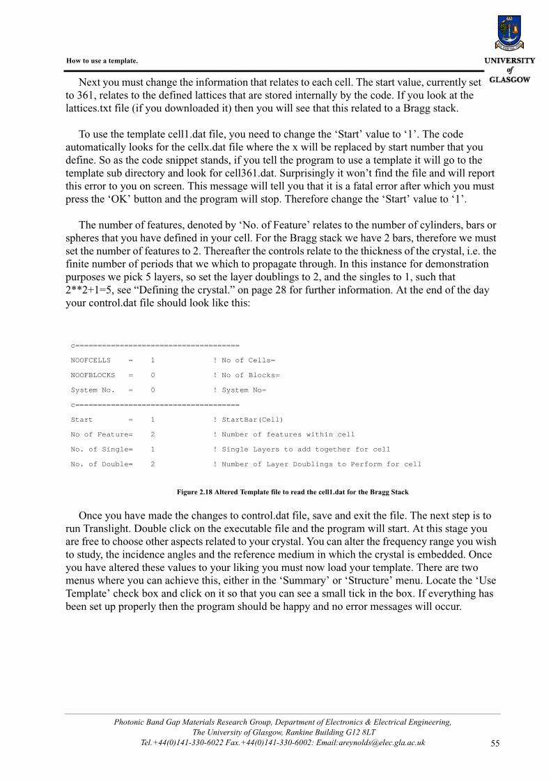
Next you must change the information that relates to each cell. The start value, currently set to 361, relates to the defined lattices that are stored internally by the code. If you look at the lattices.txt file (if you downloaded it) then you will see that this related to a Bragg stack.
To use the template cell1.dat file, you need to change the ‘Start’ value to ‘1’. The code automatically looks for the cellx.dat file where the x will be replaced by start number that you define. So as the code snippet stands, if you tell the program to use a template it will go to the template sub directory and look for cell361.dat. Surprisingly it won’t find the file and will report this error to you on screen. This message will tell you that it is a fatal error after which you must press the ‘OK’ button and the program will stop. Therefore change the ‘Start’ value to ‘1’.
The number of features, denoted by ‘No. of Feature’ relates to the number of cylinders, bars or spheres that you have defined in your cell. For the Bragg stack we have 2 bars, therefore we must set the number of features to 2. Thereafter the controls relate to the thickness of the crystal, i.e. the finite number of periods that we which to propagate through. In this instance for demonstration purposes we pick 5 layers, so set the layer doublings to 2, and the singles to 1, such that 2**2+1=5, see “Defining the crystal.” on page 28 for further information. At the end of the day your control.dat file should look like this:
Once you have made the changes to control.dat file, save and exit the file. The next step is to run Translight. Double click on the executable file and the program will start. At this stage you are free to choose other aspects related to your crystal. You can alter the frequency range you wish to study, the incidence angles and the reference medium in which the crystal is embedded. Once you have altered these values to your liking you must now load your template. There are two menus where you can achieve this, either in the ‘Summary’ or ‘Structure’ menu. Locate the ‘Use Template’ check box and click on it so that you can see a small tick in the box. If everything has been set up properly then the program should be happy and no error messages will occur.
Figure 2.18 Altered Template file to read the cell1.dat for the Bragg Stack
c=====================================NOOFCELLS = 1 ! No of Cells=NOOFBLOCKS = 0 ! No of Blocks=System No. = 0 ! System No=c=====================================Start = 1 ! StartBar(Cell)No of Feature= 2 ! Number of features within cellNo. of Single= 1 ! Single Layers to add together for cellNo. of Double= 2 ! Number of Layer Doublings to Perform for cell
Photonic Band Gap Materials Research Group, Department of Electronics & Electrical Engineering, The University of Glasgow, Rankine Building G12 8LT
Tel.+44(0)141-330-6022 Fax.+44(0)141-330-6002: Email:[email protected] 55
Tutorial 1: Omni-directional reflectance from a Bragg stack using Dmitry Chigrin’s structure.
Check list for problems with using templates.
If the program encounters an error or crashes, check that:
i) You have set up the cell.dat files correctly and that the formatting of the file is correct.
ii) You have altered the control.dat file such that the start numbers agree with the cell numbers.
iii) You have not asked the program to read a feature that doesn’t exist i.e. don’t ask the program to read information for three cylinders when you have only defined two in the cell file.
iv) Check the ‘Reports’ subdirectory and check the output.dat, runtimerrs.dat and debug.dat files, these files may give you some insight into the problem.
v) Check that you are not using the template layout for bars to define cylinders and spheres and vice versa, see “Template File Differences.” on page 58
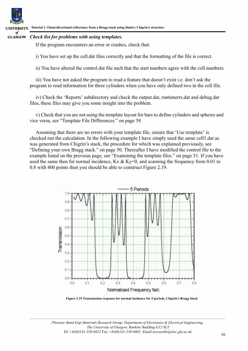
Assuming that there are no errors with your template file, ensure that ‘Use template’ is checked run the calculation. In the following example I have simply used the same cell1.dat as was generated from Chigrin’s stack, the procedure for which was explained previously, see “Defining your own Bragg stack.” on page 50. Thereafter I have modified the control file to the example listed on the previous page, see “Examining the template files.” on page 51. If you have used the same then for normal incidence, Kx & Ky=0, and scanning the frequency from 0.01 to 0.8 with 400 points then you should be able to construct Figure 2.19.
Figure 2.19 Transmission response for normal incidence for 5 periods, Chigrin’s Bragg Stack
Photonic Band Gap Materials Research Group, Department of Electronics & Electrical Engineering, The University of Glasgow, Rankine Building G12 8LT
Tel.+44(0)141-330-6022 Fax.+44(0)141-330-6002: Email:[email protected]
How to use a template.
From this plot we can instantly see that we have the response for five periods of crystal by counting the maxima in transmission leading up to the first band gap. Including the zero frequency peak there are five maxima which tell us that we have a crystal five periods thick.
Changing the template file to introduce a defect into the lattice.
To be written.
Photonic Band Gap Materials Research Group, Department of Electronics & Electrical Engineering, The University of Glasgow, Rankine Building G12 8LT
Tel.+44(0)141-330-6022 Fax.+44(0)141-330-6002: Email:[email protected] 57
Tutorial 1: Omni-directional reflectance from a Bragg stack using Dmitry Chigrin’s structure.
2.8: Template File Differences.
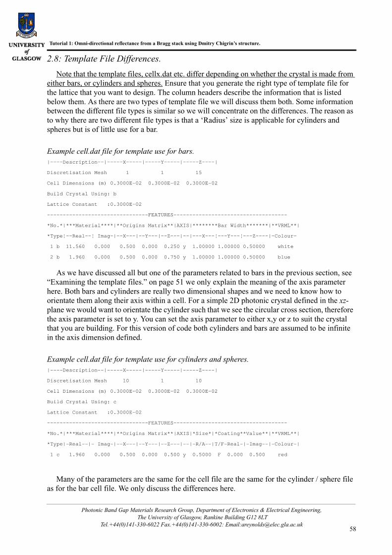
Note that the template files, cellx.dat etc. differ depending on whether the crystal is made from either bars, or cylinders and spheres. Ensure that you generate the right type of template file for the lattice that you want to design. The column headers describe the information that is listed below them. As there are two types of template file we will discuss them both. Some information between the different file types is similar so we will concentrate on the differences. The reason as to why there are two different file types is that a ‘Radius’ size is applicable for cylinders and spheres but is of little use for a bar.
Example cell.dat file for template use for bars.
As we have discussed all but one of the parameters related to bars in the previous section, see “Examining the template files.” on page 51 we only explain the meaning of the axis parameter here. Both bars and cylinders are really two dimensional shapes and we need to know how to orientate them along their axis within a cell. For a simple 2D photonic crystal defined in the xz- plane we would want to orientate the cylinder such that we see the circular cross section, therefore the axis parameter is set to y. You can set the axis parameter to either x,y or z to suit the crystal that you are building. For this version of code both cylinders and bars are assumed to be infinite in the axis dimension defined.
Example cell.dat file for template use for cylinders and spheres.
Many of the parameters are the same for the cell file are the same for the cylinder / sphere file as for the bar cell file. We only discuss the differences here.
|----Description--|-----X-----|-----Y-----|-----Z----|Discretisation Mesh 1 1 15Cell Dimensions (m) 0.3000E-02 0.3000E-02 0.3000E-02Build Crystal Using: bLattice Constant :0.3000E-02--------------------------------FEATURES------------------------------------*No.*|***Material****|**Origins Matrix**|AXIS|********Bar Width*******|**VRML**|*Type¦--Real--¦ Imag-|--X---|--Y---|--Z---|--|---X---¦---Y---¦---Z----|-Colour- 1 b 11.560 0.000 0.500 0.000 0.250 y 1.00000 1.00000 0.50000 white 2 b 1.960 0.000 0.500 0.000 0.750 y 1.00000 1.00000 0.50000 blue
|----Description--|-----X-----|-----Y-----|-----Z----|Discretisation Mesh 10 1 10Cell Dimensions (m) 0.3000E-02 0.3000E-02 0.3000E-02Build Crystal Using: cLattice Constant :0.3000E-02--------------------------------FEATURES------------------------------------*No.*|***Material****|**Origins Matrix**|AXIS|*Size*|*Coating**Value**|**VRML**|*Type|-Real--|- Imag-|--X---|--Y---|--Z---|--|-R/A--|T/F-Real-|-Imag--|-Colour-| 1 c 1.960 0.000 0.500 0.000 0.500 y 0.5000 F 0.000 0.500 red
Photonic Band Gap Materials Research Group, Department of Electronics & Electrical Engineering, The University of Glasgow, Rankine Building G12 8LT
Tel.+44(0)141-330-6022 Fax.+44(0)141-330-6002: Email:[email protected]

Template File Differences.
For cylinders and spheres we can define a radius. This is the r/a parameter which is the ratio of the size of the shape to the lattice constant. In the above file this is the ‘Size R/A’ column. For cylinders and spheres we can also apply a coating. The coatings parameters include a logical switch, T/F and the material for the coating expressed as a complex dielectric constant material. The thickness of the coating is controlled from within the program and within this version of code is assumed to be the same thickness for all the shapes that are to be coated. Coatings will only be applied to non touching areas of shapes, e.g. two merged shapes will only have a coating applied over the outer surface.
Photonic Band Gap Materials Research Group, Department of Electronics & Electrical Engineering, The University of Glasgow, Rankine Building G12 8LT
Tel.+44(0)141-330-6022 Fax.+44(0)141-330-6002: Email:[email protected] 59

Tutorial 1: Omni-directional reflectance from a Bragg stack using Dmitry Chigrin’s structure.
Photonic Band Gap Materials Research Group, Department of Electronics & Electrical Engineering, The University of Glasgow, Rankine Building G12 8LT
Tel.+44(0)141-330-6022 Fax.+44(0)141-330-6002: Email:[email protected]