tutorials for layout, drc, and lvs - georgia institute of...
TRANSCRIPT
Tutorials for Layout, DRC, and LVS
Sheng-Yu Peng10/27/2007

Create New Library from Library ManagerFile New Library…
Attach the existing tech library --> TSMC 0.4u CMOS035 (4M, 2P, HV FET)

Create Schematic Cell ViewFile New Cell View…

Instantiate NMOS and PMOSAdd Instance i

Change the Model name to be the EKV Models

Add PinsAdd Pin …p

Create Layout Cell View from Library ManagerFile New Cell View

Set the X, Y snapping spacesOption Display …e
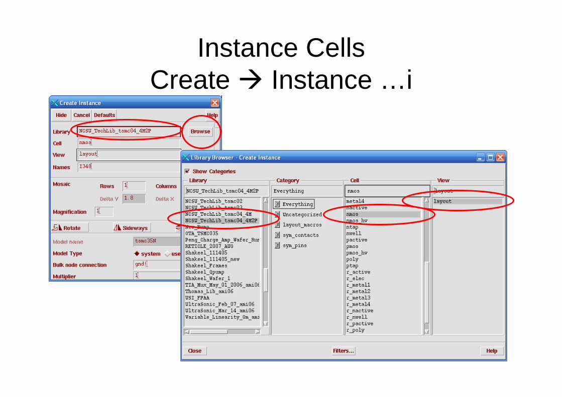
Instance CellsCreate Instance …i

Make connections with the appropriate layers

Create ContactsCreate Contact … o
Via1 Poly Contact P-sub Contact N-well Contact
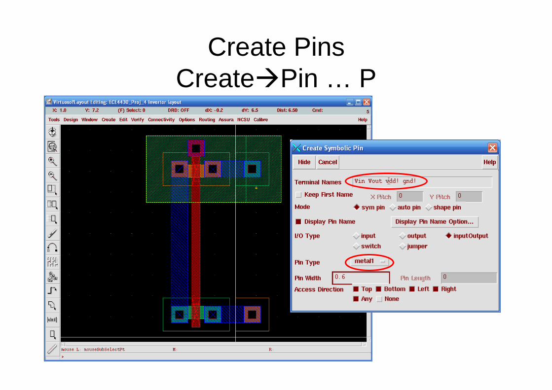
Create PinsCreate Pin … P

Place the Pins Properly and Save

Run DRC Verify DRC…

Check the DRC errors
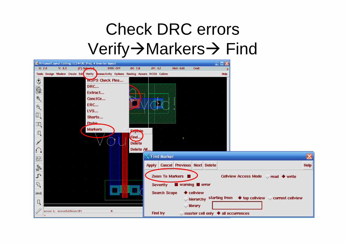
Check DRC errorsVerify Markers Find


Correct the Layout error

Extract the LayoutVerify Extract…

Layout Verify with SchematicVerify LVS…
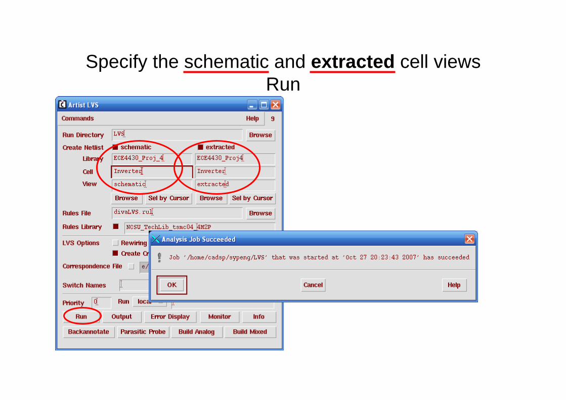
Specify the schematic and extracted cell viewsRun

Check the LVS ResultsOutput

LVS Error DisplayShort the Vout and gnd! on purpose

Extracted and Run LVS

LVS not match from the Output file
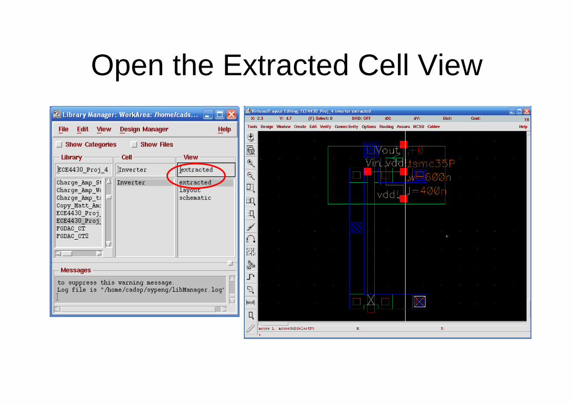
Open the Extracted Cell View
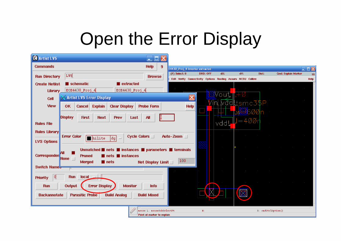
Open the Error Display

Open the Schematic Cell View
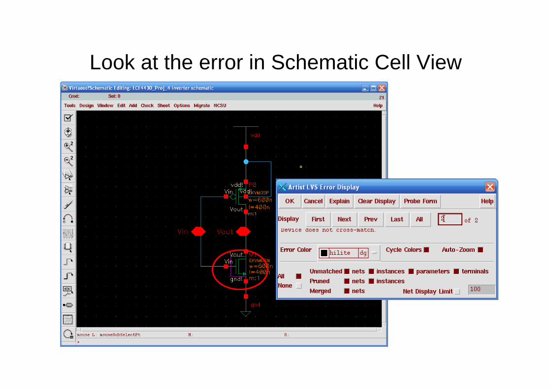
Look at the error in Schematic Cell View

Correct the Layout, DRC, Extract, and LVS

DRC Free and LVS Matched