ucc3941-5
TRANSCRIPT

SLUS242B – JANUARY 1999 – REVISED JUNE 2001
1www.ti.com
1-V Input Voltage Operation Start-upEnsured Under Full Load on Main OutputWith Operation Down to 0.4 V
Input Voltage Range of 1 V to VOUT + 0.5 V
500-mW Output Power at Battery Voltagesas Low as 0.8 V
Secondary 9-V Supply From a SingleInductor
Adjustable Output Power Limit Control
Output Fully Disconnected in Shutdown
Adaptive Current-Mode Control forOptimum Efficiency
8-µA Shutdown Supply Current
description
The UCC3941 family of low-input-voltage single-inductor boost-converters are optimized to operate from asingle- or dual-alkaline cell, and step up to a 3.3-V, 5-V, or an adjustable output at 500 mW. The UCC3941 familyalso provides an auxiliary 9-V, 100-mW output, primarily for the gate drive supply, which can be used forapplications requiring an auxiliary output such as a 5-V supply by linear regulating. The primary output startsup under full load at input voltages typically as low as 0.8 V, with a guaranteed maximum of 1 V, and operatesdown to 0.4 V once the converter is operating, maximizing battery utilization.
Demanding applications such as pagers and personal digital assistants require high efficiency from severalmilliwatts to several hundred milliwatts, and the UCC3941 family accommodates these applications with > 80%typical efficiencies over the wide range of operation. The high-efficiency at low-output current is achieved byoptimizing switching and conduction losses along with low-quiescent current. At higher output current the0.25-Ω charge switch, and the 0.4-Ω synchronous rectifier, along with continuous-mode conduction, providehigh efficiency. The wide input-voltage range on the UCC3941 family can accommodate other power sourcessuch as NiCd and NiMH.
Other features include maximum power control and shutdown control. The device is available in 8-pin SOIC (D)and 8-pin DIP (N).
AVAILABLE OPTIONS
PACKAGED DEVICES
SOIC (D)† DIP (N)
TA VOUT (V)A
3.3 5.0Adjustable
(1.3 V to 6 V)3.3 5.0
Adjustable(1.3 V to 6 V)
–40C to 85C UCC2941D–3 UCC2941D–5 UCC2941D–ADJ UCC2941N–3 UCC2941N–5 UCC2941N–ADJ
0C to 70C UCC3941D–3 UCC3941D–5 UCC3941D–ADJ UCC3941N–3 UCC3941N–5 UCC3941N–ADJ† The SOIC (D) package is available left end taped and reeled. Add an R suffix to the device type (e.g., UCC2941DR–3) to order
quantities of 2500 devices per reel.
Copyright 2001, Texas Instruments Incorporated !"#$ % &'!!($ #% )'*+&#$ ,#$(-! ,'&$% & !" $ %)(&&#$ % )(! $.( $(!"% (/#% %$!'"($%%$#,#!, 0#!!#$1- ! ,'&$ )! &(%%2 , (% $ (&(%%#!+1 &+',($(%$2 #++ )#!#"($(!%-
Please be aware that an important notice concerning availability, standard warranty, and use in critical applications ofTexas Instruments semiconductor products and disclaimers thereto appears at the end of this data sheet.
D OR N PACKAGE(TOP VIEW)
1
2
3
4
8
7
6
5
VOUTVGDVINSD
SWPGNDSGNDPLIM
1
2
3
4
8
7
6
5
VOUTVGDVINSD
SWPGNDFBPLIM
UCC3941–ADJ ONLY(TOP VIEW)
SLUS242B – JANUARY 1999 – REVISED JUNE 2001
2 www.ti.com
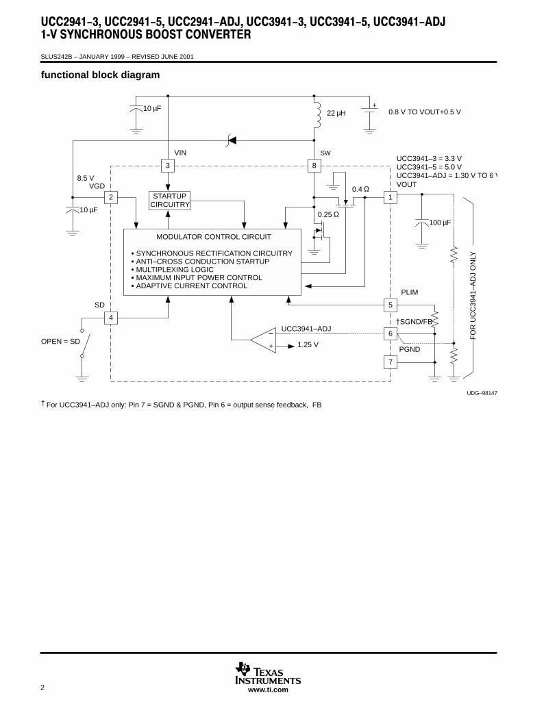
functional block diagram
UDG–98147
MODULATOR CONTROL CIRCUIT
4
5
6
7
1
83
2
1.25 V
UCC3941–ADJ
OPEN = SD
SD
10 µF
VGD8.5 V
STARTUPCIRCUITRY
VIN SW
+10 µF22 µH
100 µF
0.4 Ω VOUT
PGND
PLIM
0.25 Ω
UCC3941–3 = 3.3 VUCC3941–5 = 5.0 VUCC3941–ADJ = 1.30 V TO 6 V
FO
R U
CC
3941
–AD
J O
NLY
+
SGND/FB
SYNCHRONOUS RECTIFICATION CIRCUITRY ANTI–CROSS CONDUCTION STARTUP MULTIPLEXING LOGIC MAXIMUM INPUT POWER CONTROL ADAPTIVE CURRENT CONTROL
0.8 V TO VOUT+0.5 V
† For UCC3941–ADJ only: Pin 7 = SGND & PGND, Pin 6 = output sense feedback, FB
SLUS242B – JANUARY 1999 – REVISED JUNE 2001
3www.ti.com
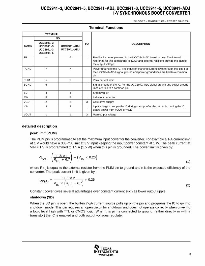
Terminal Functions
TERMINAL
NO.
NAMEUCC2941–3UCC2941–5UCC3941–3UCC3941–5
UCC2941–ADJUCC3941–ADJ
I/O DESCRIPTION
FB – 6 I Feedback control pin used in the UCC3941–ADJ version only. The internalreference for this comparator is 1.25V and external resistors provide the gain tothe output voltage.
PGND 7 7 – Power ground of the IC. The inductor charging current flows through this pin. Forthe UCC3941–ADJ signal ground and power ground lines are tied to a commonpin.
PLIM 5 5 I Peak current limit
SGND 6 – – Signal ground of the IC. For the UCC3941–ADJ signal ground and power groundlines are tied to a common pin
SD 4 4 I Shutdown pin
SW 8 8 I Inductor connection
VGD 2 2 O Gate drive supply
VIN 3 3 I Input voltage to supply the IC during startup. After the output is running the ICdraws power from VOUT or VGD
VOUT 1 1 O Main output voltage
detailed description
peak limit (PLIM)
The PLIM pin is programmed to set the maximum input power for the converter. For example a 1-A current limitat 1 V would have a 333-mA limit at 3 V input keeping the input power constant at 1 W. The peak current atVIN = 1 V is programmed to 1.5 A (1.5 W) when this pin is grounded. The power limit is given by:
PLW 11.8 nRPL 6.7
VIN 0.26
where RPL is equal to the external resistor from the PLIM pin to ground and n is the expected efficiency of theconverter. The peak current limit is given by:
IPK(A) 11.8 n
VIN RPL 6.7 0.26
Constant power gives several advantages over constant current such as lower output ripple.
shutdown (SD)
When the SD pin is open, the built-in 7-µA current source pulls up on the pin and programs the IC to go intoshutdown mode. This pin requires an open circuit for shutdown and does not operate correctly when driven toa logic level high with TTL or CMOS logic. When this pin is connected to ground, (either directly or with atransistor) the IC is enabled and both output voltages regulate.
(1)
(2)

SLUS242B – JANUARY 1999 – REVISED JUNE 2001
4 www.ti.com
detailed description (continued)
needs a name (SW)
The SW pin inductor is connected between this node and VIN. The VGD (gate drive supply) flyback diode isalso connected to this pin. When servicing the 3.3-V supply, this pin goes low charging the inductor, then shutoff, dumping the energy through the synchronous rectifier to the output. When servicing the VGD supply, theinternal synchronous rectifier stays off, and the energy is diverted to VGD through the flyback diode. Duringdiscontinuous portions of the inductor current a MOSFET resistively connects VIN to SW damping excesscirculating energy to eliminate undesired high frequency ringing.
gate drive supply (VGD)
The VGD pin is coarsely regulated around 9 V, and is primarily used for the gate drive supply for the powerswitches in the IC. This pin can be loaded with up to 10 mA as long as it does not present a load at voltagesbelow 2 V. This ensures proper startup of the IC. The VGD supply can go as low as 7.5 V without interferingwith the servicing of the 3.3-V output. Below 7.5 V, VGD has the highest priority, although in practice the voltageshould not decay to that level if the output capacitor is sized properly.
output voltage (VOUT)
Main output voltage (3.3 V, 5 V, or adjustable) which has highest priority in the multiplexing scheme, as longas VGD is above the critical level of 7.5 V. Loads over 150 mA are achievable at an input voltage of 1-V. Thisoutput starts up with 1-V input at full load.
absolute maximum ratings over operating free–air temperature range (unless otherwise noted)†
Input voltage VIN, PLIM –0.3 V to 10 V. . . . . . . . . . . . . . . . . . . . . . . . . . . . . . . . . . . . . . . . . . . . . . . . . . . . . . . . . . . . Voltage range, VGD, SW –0.3 V to 15 V. . . . . . . . . . . . . . . . . . . . . . . . . . . . . . . . . . . . . . . . . . . . . . . . . . . . . . . . . . . Voltage range, SD –0.3 V to VIN. . . . . . . . . . . . . . . . . . . . . . . . . . . . . . . . . . . . . . . . . . . . . . . . . . . . . . . . . . . . . . . . . . Output voltage range, VOUT –0.3 V to 10 V. . . . . . . . . . . . . . . . . . . . . . . . . . . . . . . . . . . . . . . . . . . . . . . . . . . . . . . . Operating virtual junction temperature range, TJ –55C to 150C. . . . . . . . . . . . . . . . . . . . . . . . . . . . . . . . . . . . . . Storage temperature range, Tstg –65C to 150C. . . . . . . . . . . . . . . . . . . . . . . . . . . . . . . . . . . . . . . . . . . . . . . . . . . . Lead temperature soldering 1,6 mm (1/16 inch) from case for 10 seconds 300C. . . . . . . . . . . . . . . . . . . . . . . CDM 1 kV. . . . . . . . . . . . . . . . . . . . . . . . . . . . . . . . . . . . . . . . . . . . . . . . . . . . . . . . . . . . . . . . . . . . . . .
† Stresses beyond those listed under “absolute maximum ratings” may cause permanent damage to the device. These are stress ratings only, andfunctional operation of the device at these or any other conditions beyond those indicated under “recommended operating conditions” is notimplied. Exposure to absolute–maximum–rated conditions for extended periods may affect device reliability. Currents are positive into, negativeout of the specified terminal.
DISSIPATION RATING TABLE
PACKAGE TA ≤ 25CPOWER RATING
DERATING FACTORABOVE TA = 25C
TA = 85CPOWER RATING
D 760 mW 6.1 mW/C 390 mW
N 980 mW 7.9 mW/C 510 mW
recommended operating conditionsMIN MAX UNIT
Input voltage 0.8 5.0 V
Output voltage 1.8 5.5 V
Output current 0 200 mA
SLUS242B – JANUARY 1999 – REVISED JUNE 2001
5www.ti.com
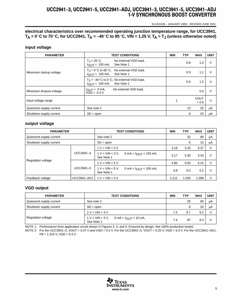
electrical characteristics over recommended operating junction temperature range, for UCC3941,TA = 0C to 70C, for UCC2941, TA = –40C to 85C, VIN = 1.25 V, TA = TJ (unless otherwise noted)
input voltage
PARAMETER TEST CONDITIONS MIN TYP MAX UNIT
TJ = 25C, No external VGD load,IOUT = 100 mA, See Note 1
0.8 1.0 V
Minumum startup voltageTJ = 0C to 85C, No external VGD load,IOUT = 100 mA, See Note 1
0.9 1.1 V
TJ = –40C to 0C, No external VGD load,IOUT = 100 mA, See Note 1
0.9 1.5 V
Minumum dropout voltageIOUT = 0 mA, No external VGD load,VGD = 6.3 V 0.5 V
Input voltage range 1VOUT+ 0.5
V
Quiescent supply current See note 2 13 25 µA
Shutdown supply current SD = open 8 20 µA
output voltage
PARAMETER TEST CONDITIONS MIN TYP MAX UNIT
Quiescent supply current See note 2 32 80 µA
Shutdown supply current SD = open 6 15 µA
1 V < VIN < 3 V 3.18 3.25 3.37 V
Regulation voltage
UCC3941–3 1 V < VIN < 3 V, 0 mA < IOUT < 150 mA,See Note 1
3.17 3.30 3.43 V
Regulation voltage1 V < VIN < 5 V 4.85 5.00 5.15 V
UCC3941–5 1 V < VIN < 5 V, 0 mA < IOUT < 100 mA, See Note 1
4.8 5.0 5.2 V
Feedback voltage UCC3941–ADJ 1 V < VIN < 3 V 1.212 1.250 1.288 V
VGD output
PARAMETER TEST CONDITIONS MIN TYP MAX UNIT
Quiescent supply current See note 2 25 60 µA
Shutdown supply current SD = open 8 20 µA
1 V < VIN < 3 V 7.5 8.7 9.2 V
Regulation voltage 1 V < VIN < 3 V, 0 mA < IOUT < 10 mA,See Note 1
7.4 87 9.3 V
NOTE 1: Performance from application circuit shown in Figures 3, 4, and 5. Ensured by design. Not 100% production tested.NOTE 2: For the UCC3941–3, VOUT = 3.47 V and VGD = 9.3 V. For the UCC3941–5, VOUT = 5.25 V, VGD = 9.3 V. For the UCC3941–ADJ,
FB = 1.315 V, VGD = 9.3 V.

SLUS242B – JANUARY 1999 – REVISED JUNE 2001
6 www.ti.com
electrical characteristics over recommended operating junction temperature range, for UCC3941,TA = 0C to 70C, for UCC2941, TA = –40C to 85C, VIN = 1.25 V, TA = TJ (unless otherwise noted)(continued)
inductor charging (L = 22 µH)
PARAMETER TEST CONDITIONS MIN TYP MAX UNIT
Peak discontinuous current Over operating range 0.05 0.85 A
Peak continuous current RPLIM = 6.2 Ω, See Note 1 0.5 0.9 1.3 A
Charge switch RDS(on) N and D package, I = 200 mA 0.25 0.40 Ω
Current limit delay See Note 1 50 ns
synchronous rectifier
PARAMETER TEST CONDITIONS MIN TYP MAX UNIT
UCC3941N–ADJUCC3941D–ADJ
I = 200 mA, VOUT = 3.3 V 0.35 0.6 Ω
Rectifier RDS(on)UCC3941N–3UCC3941D–3
I = 200 mA 0.35 0.6 Ω
UCC3941N–5UCC3941D–5
I = 200 mA 0.5 0.8 Ω
shutdown
PARAMETER TEST CONDITIONS MIN TYP MAX UNIT
Shutdown bias current SD = 0 V –10 –7 µA
NOTE 1: Performance from application circuit shown in Figures 3, 4, and 5. Ensured by design. Not 100% production tested.NOTE 2: For the UCC3941–3, VOUT = 3.47 V and VGD = 9.3 V. For the UCC3941–5, VOUT = 5.25 V, VGD = 9.3 V. For the UCC3941–ADJ,
FB = 1.315 V, VGD = 9.3 V.

SLUS242B – JANUARY 1999 – REVISED JUNE 2001
7www.ti.com
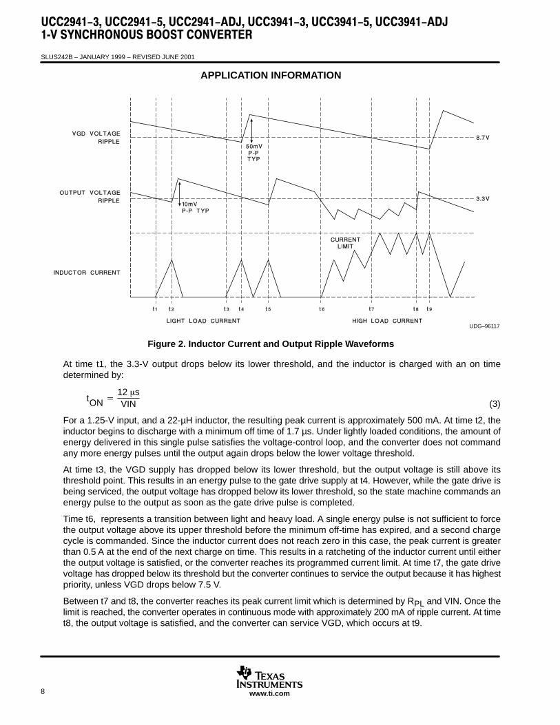
APPLICATION INFORMATION
A detailed block diagram of the UCC3941 is shown in Figure 1. Unique control circuitry provides high-efficiencypower conversion for both light and heavy loads by transitioning between discontinuous and continuousconduction based on load conditions. Figure 2 depicts converter waveforms for the application circuit shownin Figure 3. A single 22-µH inductor provides the energy pulses required for a highly efficient 3.3-V converterat up to 500 mW output power.
UDG–98146
4
5
2
3 8
1
6
6
7
SD
PLIM
VGD
VIN SW
VOUT
FB(UCC3941–ADJONLY)
PGND
SGND(UCC3941–3/–5ONLY)
5 Ω
VGD
* 3.3 V FOR UCC3941–35.0 V FOR UCC3941–5
1.25 V FOR UCC3941–ADJ
VGD
** 8.7 V FOR UCC3941–39.6 V FOR UCC3941–5/–ADJ
VGD
*** 7.7 V FOR UCC3941–38.8 V FOR UCC3941–5/–ADJ
FROMSD
5V
1.1 AMAX
CURRENTLIMIT
50 mVVIN
VINSD
50 mVMAXIMUM
200 kHzSTARTUP
OSCILLATORAND CONTROL
VGD
VGD
VGD ZERODETECT
VOUT ZERODETECT
ANTI–RINGINGSWITCH
1.7 µSOFF TIME
CONTROLLER
RECTIFIERCONTROLFROM SD
CLK
D QL1
R Q
SD
BOOSTLATCH
ON TIMECONTROLLER
TON=11 µSEC
VIN
VSAT
*
**
***
THERMALSHUTDOWN
RQ
SD
+
+
+
+
+
+
+
NOTE: Switches are shown in the logic low state; external RPLIM = 6.2 Ω
Figure 1. 1–V Synchronous Boost
SLUS242B – JANUARY 1999 – REVISED JUNE 2001
8 www.ti.com
APPLICATION INFORMATION
UDG–96117
Figure 2. Inductor Current and Output Ripple Waveforms
At time t1, the 3.3-V output drops below its lower threshold, and the inductor is charged with an on timedetermined by:
tON 12 sVIN
For a 1.25-V input, and a 22-µH inductor, the resulting peak current is approximately 500 mA. At time t2, theinductor begins to discharge with a minimum off time of 1.7 µs. Under lightly loaded conditions, the amount ofenergy delivered in this single pulse satisfies the voltage-control loop, and the converter does not commandany more energy pulses until the output again drops below the lower voltage threshold.
At time t3, the VGD supply has dropped below its lower threshold, but the output voltage is still above itsthreshold point. This results in an energy pulse to the gate drive supply at t4. However, while the gate drive isbeing serviced, the output voltage has dropped below its lower threshold, so the state machine commands anenergy pulse to the output as soon as the gate drive pulse is completed.
Time t6, represents a transition between light and heavy load. A single energy pulse is not sufficient to forcethe output voltage above its upper threshold before the minimum off-time has expired, and a second chargecycle is commanded. Since the inductor current does not reach zero in this case, the peak current is greaterthan 0.5 A at the end of the next charge on time. This results in a ratcheting of the inductor current until eitherthe output voltage is satisfied, or the converter reaches its programmed current limit. At time t7, the gate drivevoltage has dropped below its threshold but the converter continues to service the output because it has highestpriority, unless VGD drops below 7.5 V.
Between t7 and t8, the converter reaches its peak current limit which is determined by RPL and VIN. Once thelimit is reached, the converter operates in continuous mode with approximately 200 mA of ripple current. At timet8, the output voltage is satisfied, and the converter can service VGD, which occurs at t9.
(3)

SLUS242B – JANUARY 1999 – REVISED JUNE 2001
9www.ti.com
APPLICATION INFORMATION
programming the power limit
The UCC3941 incorporates an adaptive power limit control that modifies the converter current limit as a functionof input voltage. In order to program the function, the user simply determines the output power requirementsand makes an initial converter efficiency estimate. The programming resistor is chosen by:
RPL 11.8 n
POUT 0.26 n VBAT 6.7
Where n is the initial efficiency estimate. For 500 mW of output power, with a 1.0 V input, and an efficiencyestimate of 0.75:
RPL 11.8 0.750.5 (0.26 0.75 1.0)
6.7 22
For decreasing values of RPL, the power limit increases. Therefore, to ensure that the converter can supply500 mW of output power, a power limiting resistor of less than 22 Ω must be chosen.
PL VBAT IL 11.822 6.7
(1.0 0.26) 0.67 W
UDG–98163
5
8
1
7
6
VOUT
SW
10SN100M100 µF
RPL 6.2 Ω
WCR0805–6R2074
3.3 V AT 500 mW
2
SD
VGD
10 µF
OPEN = SD
3
VIN
10 µFMMSZ5240BT1
10 V
+
1 V TO 3.5 V
DT3316P–22322 µH
PLIM
SGND
PGND
UCC3941–3
8.5 V
Figure 3. Dual Output Synchronous Boost, 3.3-V Version
(4)
(5)
(6)

SLUS242B – JANUARY 1999 – REVISED JUNE 2001
10 www.ti.com
APPLICATION INFORMATION
programming the power limit (continued)
UDG–98159
5
8
1
7
6
VOUT
SW
10SN100M100 µF
RPL 6.2 ΩWCR0805–6R207
4
5.0 V AT 500 mW
2
SD
VGD
10 µF
OPEN = SD
3
VIN
10 µFMMSZ5240BT1
10 V
+ 1 V TO 5.5 VDT3316P–22322 µH
PLIM
SGND
PGND
UCC3941–5
8.5 V
Figure 4. Dual Output Synchronous Boost, 5-V Version
UDG–98164
5
8
1
7
6
VOUT
SW
10SN100M100µF
RPL 6.2ΩWCR0805–6R207
4
2
SD
VGD
10 µF
OPEN = SD
3
VIN
10 µFMMSZ5240BT1
+ 1 V TO VOUT + 0.5 VDT3316P–223
PLIM
FB
(SGND)PGND
UCC3941–ADJ
8.5 V
R1
R2
10 V
VOUT 1.25 1 R1R2 AT 500 mA
VREF = 1.25 V
22 µH
Figure 5. Dual Output Synchronous Boost, Adjustable Version

SLUS242B – JANUARY 1999 – REVISED JUNE 2001
11www.ti.com
APPLICATION INFORMATION
programming the power limit (continued)
This power limiting setting supports 0.5 W of output power. It should be noted that the power limit equationcontains an approximation which results in slightly less actual input power than the equation predicts. Thisdiscrepancy results from the fact that the average current delivered to the load is less than the peak current setby the power limit function due to current ripple. However, if the ripple component of the current is kept low, thepower limit equation can be used as an adequate estimate of input power. Furthermore, since an initial efficiencyestimate was required, sufficient margin can be built into this estimate to ensure proper converter operation.The 6.2-Ω external power limit resistor (shown in Figures 3, 4, and 5) results in approximately 700 mW of powercapability with a 1.0-V input.
inductor selection
An inductor value of 22 µH works well in most applications, but values between 10 µH and 100 µH are alsoacceptable. Lower-value inductors typically offer lower ESR and smaller physical size. Due to the nature of thebang–bang controllers, larger inductor values typically results in larger overall voltage ripple, because once theoutput voltage level is satisfied the converter goes discontinuous, resulting in the residual energy of inductorcausing overshoot.
It is recommended to keep the ESR of the inductor below 0.15 Ω for 500-mW applications. A CoilcraftDT3316P–223 surface mount inductor is one choice since it has a current rating of 1.5 A and an ESR of 84 mΩ.Other choices for surface mount inductors are shown in Table 1.
Table 1. Inductor Suppliers
MANUFACTURER CONTACT INFORMATION PART NUMBERS
CoilcraftCary, Illinois
Tel: (708) 639–2361 Fax: (708) 639–1469DT Series
CoiltronicsBoca Raton, FloridaTel: (407) 241–7878
CTX Series

SLUS242B – JANUARY 1999 – REVISED JUNE 2001
12 www.ti.com
APPLICATION INFORMATION
output capacitor selection
Once the inductor value is selected, the capacitor value determines the ripple of the converter. The worst casepeak-to-peak ripple of a cycle is determined by two components, one is due to the charge storage characteristic,and the other is the ESR of the capacitor. The worst-case ripple occurs when the inductor is operating atmaximum current and is expressed as follows:
V ICL
2 L
2 C VO VI ICL CESR
where
ICL = the peak inductor current ICL Power LimitVIN
∆V = output ripple
VO = output voltage
VI = input voltage
CESR = ESR of the output capacitor
A Sanyo OS–CON series surface mount capacitor (10SN100M) is one recommendation. This part has an ESRrating of 90 µW at 100 µF. Other potential capacitor sources are shown in Table 2.
Table 2. Capacitor Suppliers
MANUFACTURER CONTACT INFORMATION PART NUMBERS
Sanyo Video ComponentsSan Diego, CaliforniaTel: (619) 661–6322Fax: (619) 661–1055
OS–CON Series
AVXSanford, Maine
Tel: (207) 282–5111Fax: (207) 283–1941
TPS Series
SpragueConcord, New Hampshire
Tel: (603) 224–1961695D Series
input capacitor selection
Since the UCC3941 family does not require a large decoupling capacitor on the input voltage to operateproperly, a 10-µF capacitor is sufficient for most applications. Optimum efficiency occurs when the capacitorvalue is large enough to decouple the source impedance. This usually occurs for capacitor values in excessof 100 µF.
(7)

SLUS242B – JANUARY 1999 – REVISED JUNE 2001
13www.ti.com
APPLICATION INFORMATION
system shutdown
The UCC3941 is enabled by shorting the SD pin to ground either directly or through a transistor.The UCC3941is shut down when the SD pin is floated (an internal current source pulls up on the SD pin). Since the SD pinis not TTL compatible, 0 V enables the part but 3 V or even 5 V does not properly shut down the device.
The recommended circuit for a system requiring shutdown control is shown below. The enable line is driven froma microprocessor or system logic. If enable is low, the SD pin is floated since Q1 base voltage is too low to turnon. If enable is high, Q1 turns on and SD is grounded, enabling the UCC3941. A 1-MΩ resistor to VGD allowsQ1 to turn on if the enable pin is high impedance during startup. If shutdown control is not required for theapplication, SD should be grounded directly.
CAUTION:The UCC3941 should be allowed sufficient time to properly shutdown in a controlledmanner. This is accomplished by ensuring that enable is held low at least 500 µs beforesubsequently being brought high. Not adhering to the timings in Figure 7 can result inDEVICE FAILURE.
Figure 6
2
4 SD1 MΩ
VGD
20 kΩ
ENABLE
SHUTDOWN INTERFACE CIRCUIT
500 100000
~~0
2
4
6
8
10
VS
D –
Sh
utd
ow
n V
olt
age
– V
En
able
Vo
ltag
e –
V
t – Time – µs
PROPOGATION DELAY AND RISE TIME
~~
2
4
6
Ensure 500 µs
Figure 7. SD Timings

SLUS242B – JANUARY 1999 – REVISED JUNE 2001
14 www.ti.com
APPLICATION INFORMATION
SD interface circuit
reducing inrush current
A switch mode boost converter requires VIN to be less than VOUT in order to control current in the inductor.Forward voltage is applied across the inductor during the tON time (increasing current) while reverse voltageis applied during the tOFF time (decreasing current). During startup, VOUT is less than VIN, resulting in inrushcurrent until the output is charged.
The UCC3941 has two outputs; VGD and VOUT. Inrush current in a two cell alkaline application is typically higherthan with a single cell and should be minimized to reduce peak currents in the controller. The VGD inrush currentcan be minimized by reducing the value of the VGD capacitor. For example a 10-µF capacitor may cause a 3-Ainrush where a 1-µF capacitor results in less than 1-A of inrush. Reducing the VOUT inrush current is moredifficult since the output capacitance may need to be large to minimize output ripple. In a two cell application,a diode from VIN to VOUT (shown In Figure 8) precharges the VOUT capacitor and reduces inrush.
UDG–00155
8 1
3
SW
VIN
VOUT
2 VGD
10 VZENER
+2 CELLINPUT
PRECHARGE DIODE
22 µH
220 µF
1 µF
100 µF
Figure 8. Optional Precharge Diode for VOUT for 2-Cell Input
avoiding inductor saturation
Inductor selection should take into account size, on resistance, and the current capabilities of the part. Inductorratings include both saturation current and maximum operating current for the device. The RPLIM resistor andinductor should be selected to guarantee the inductor does not saturate during normal operation. A saturatedinductor can cause excessive peak currents and δi/δt slopes which may result in part failure. Inrush and normaloperating current should be viewed with a current probe and oscilloscope to ensure the inductor current is linearand controlled.
SLUS242B – JANUARY 1999 – REVISED JUNE 2001
15www.ti.com
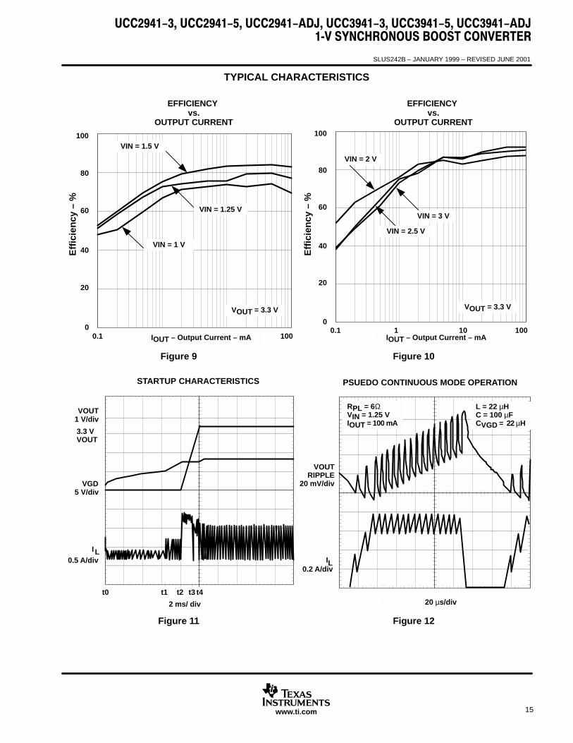
TYPICAL CHARACTERISTICS
Figure 9
Eff
icie
ncy
– %
EFFICIENCY vs.
OUTPUT CURRENT
0.1 1 10 100
20
40
60
80
100
0IOUT – Output Current – mA
VIN = 1.5 V
VIN = 1.25 V
VIN = 1 V
VOUT = 3.3 V
Figure 10
Eff
icie
ncy
– %
IOUT – Output Current – mA
EFFICIENCY vs.
OUTPUT CURRENT
0.1 1 10 100
20
40
60
80
100
0
VIN = 2 V
VIN = 3 V
VIN = 2.5 V
VOUT = 3.3 V
Figure 11
STARTUP CHARACTERISTICS
VOUT1 V/div
VGD5 V/div
I L0.5 A/div
t0 t1 t2 t4t3
2 ms/ div
3.3 VVOUT
IL0.2 A/div
Figure 12
20 µs/div
PSUEDO CONTINUOUS MODE OPERATION
VOUTRIPPLE
20 mV/div
RPL = 6ΩVIN = 1.25 VIOUT = 100 mA
L = 22 µHC = 100 µFCVGD = 22 µH

SLUS242B – JANUARY 1999 – REVISED JUNE 2001
16 www.ti.com
startup characteristics timing sequence (for single output mode)
(see Figure 11)
t0 the 200-kHz srartup oscillator starts VGD rising
t1 VGD reaches sufficient voltage (5 V) to run in normal operating mode
t2 VGD reaches sufficient voltage (7.5 V) to start VOUT
t3 VOUT is serviced and starts up
t4 VOUT reaches sufficient voltage and VGD is serviced until it reaches 8.5 V
VGD LOAD = 10 mA
VOUT LOAD = 50 mA
t1 t2 t3 t4 t5
VOUTAC COUPLED50 mV/DIV
VGDAC COUPLED100 mV/DIV
INDUCTORCURRENT200 mA/DIV
Figure 13.
startup characteristics timing sequence (for dual output mode)
(see Figure 13)
t1 VOUT is serviced and inductor current goes continuous
t2 VGD is serviced with discontinuous operation and reaches its first threshold (7.5 V)
t3 VOUT requires servicing and because VGD has reached its minimum threshold of 7.5 V, VOUT takes priority
t4 VOUT is satisfied and VGD is serviced until the second threshold (8.7 V) is reached
t5 Both outputs are satisfied

SLUS242B – JANUARY 1999 – REVISED JUNE 2001
17www.ti.com
TYPICAL CHARACTERISTICS
Figure 14
VIN
– D
rop
ou
t V
olt
age
– V
UCC3941–3 DROPOUT VOLTAGE vs.
OUTPUT CURRENT
IOUT – Output Current – mA0 50 100 150
0.6
1.2
1.0
0.8
0.4
0.2
0
Figure 15
IOUT – Output Current – mA
MINIMUM STARTUP VOLTAGEvs.
OUTPUT CURRENT
0
0.84
0.80
0.96
0.92
1.04
1.00
1.12
1.08
1.16
50 100 150
0.88
1.20
VIN
– S
tart
up
Vo
ltag
e –
V
Figure 16
0 2 4 6 8 10 12 14 16 18 20
0.5
0.3
0.9
0.7
1.3
1.1
1.7
1.5
1.9
2.1
RP – Programming Resistance – Ω
UCC3941–ADJ (N and D PACKAGES) CURRENT LIMITvs.
PROGRAMMING RESISTANCE
I L –
Cu
rren
t L
imit
– A
VIN = 1 V
VIN = 1.25 V
VIN = 1.5 V
VIN = 1.75 V
VIN = 2 V
VIN = 3 V
IL(Rp) 11.5
6.7 RP VBAT
0.26
Figure 17
Temperature – C
STARTUP VOLTAGEvs.
TEMPERATURE
VIN
– S
tart
up
Vo
ltag
e –
V
–40 –20 0 8020 10040 60
0.2
0
0.4
0.6
0.8
1.0
1.2

PACKAGE OPTION ADDENDUM
www.ti.com 17-Mar-2011
Addendum-Page 1
PACKAGING INFORMATION
Orderable Device Status (1) Package Type PackageDrawing
Pins Package Qty Eco Plan (2) Lead/Ball Finish
MSL Peak Temp (3) Samples
(Requires Login)
UCC2941D-5 LIFEBUY SOIC D 8 TBD Call TI Call TI
UCC2941D-5G4 LIFEBUY SOIC D 8 TBD Call TI Call TI
UCC2941D-ADJ LIFEBUY SOIC D 8 TBD Call TI Call TI
UCC2941D-ADJG4 LIFEBUY SOIC D 8 TBD Call TI Call TI
UCC2941N-5 LIFEBUY PDIP P 8 TBD Call TI Call TI
UCC2941N-5G4 LIFEBUY PDIP P 8 TBD Call TI Call TI
UCC3941D-5 LIFEBUY SOIC D 8 TBD Call TI Call TI
UCC3941D-5G4 LIFEBUY SOIC D 8 TBD Call TI Call TI
UCC3941D-ADJ LIFEBUY SOIC D 8 TBD Call TI Call TI
UCC3941D-ADJG4 LIFEBUY SOIC D 8 TBD Call TI Call TI
UCC3941DTR-3 LIFEBUY SOIC D 8 TBD Call TI Call TI
UCC3941DTR-3G4 LIFEBUY SOIC D 8 TBD Call TI Call TI
UCC3941DTR-ADJ LIFEBUY SOIC D 8 TBD Call TI Call TI
UCC3941DTR-ADJG4 LIFEBUY SOIC D 8 TBD Call TI Call TI
UCC3941N-3 LIFEBUY PDIP P 8 TBD Call TI Call TI
UCC3941N-3G4 LIFEBUY PDIP P 8 TBD Call TI Call TI
UCC3941N-5 LIFEBUY PDIP P 8 TBD Call TI Call TI
UCC3941N-5G4 LIFEBUY PDIP P 8 TBD Call TI Call TI
UCC3941N-ADJ LIFEBUY PDIP P 8 TBD Call TI Call TI
UCC3941N-ADJG4 LIFEBUY PDIP P 8 TBD Call TI Call TI (1) The marketing status values are defined as follows:ACTIVE: Product device recommended for new designs.LIFEBUY: TI has announced that the device will be discontinued, and a lifetime-buy period is in effect.NRND: Not recommended for new designs. Device is in production to support existing customers, but TI does not recommend using this part in a new design.PREVIEW: Device has been announced but is not in production. Samples may or may not be available.OBSOLETE: TI has discontinued the production of the device.
(2) Eco Plan - The planned eco-friendly classification: Pb-Free (RoHS), Pb-Free (RoHS Exempt), or Green (RoHS & no Sb/Br) - please check http://www.ti.com/productcontent for the latest availabilityinformation and additional product content details.TBD: The Pb-Free/Green conversion plan has not been defined.Pb-Free (RoHS): TI's terms "Lead-Free" or "Pb-Free" mean semiconductor products that are compatible with the current RoHS requirements for all 6 substances, including the requirement thatlead not exceed 0.1% by weight in homogeneous materials. Where designed to be soldered at high temperatures, TI Pb-Free products are suitable for use in specified lead-free processes.
PACKAGE OPTION ADDENDUM
www.ti.com 17-Mar-2011
Addendum-Page 2
Pb-Free (RoHS Exempt): This component has a RoHS exemption for either 1) lead-based flip-chip solder bumps used between the die and package, or 2) lead-based die adhesive used betweenthe die and leadframe. The component is otherwise considered Pb-Free (RoHS compatible) as defined above.Green (RoHS & no Sb/Br): TI defines "Green" to mean Pb-Free (RoHS compatible), and free of Bromine (Br) and Antimony (Sb) based flame retardants (Br or Sb do not exceed 0.1% by weightin homogeneous material)
(3) MSL, Peak Temp. -- The Moisture Sensitivity Level rating according to the JEDEC industry standard classifications, and peak solder temperature.
Important Information and Disclaimer:The information provided on this page represents TI's knowledge and belief as of the date that it is provided. TI bases its knowledge and belief on informationprovided by third parties, and makes no representation or warranty as to the accuracy of such information. Efforts are underway to better integrate information from third parties. TI has taken andcontinues to take reasonable steps to provide representative and accurate information but may not have conducted destructive testing or chemical analysis on incoming materials and chemicals.TI and TI suppliers consider certain information to be proprietary, and thus CAS numbers and other limited information may not be available for release.
In no event shall TI's liability arising out of such information exceed the total purchase price of the TI part(s) at issue in this document sold by TI to Customer on an annual basis.
IMPORTANT NOTICE
Texas Instruments Incorporated and its subsidiaries (TI) reserve the right to make corrections, modifications, enhancements, improvements,and other changes to its products and services at any time and to discontinue any product or service without notice. Customers shouldobtain the latest relevant information before placing orders and should verify that such information is current and complete. All products aresold subject to TI’s terms and conditions of sale supplied at the time of order acknowledgment.
TI warrants performance of its hardware products to the specifications applicable at the time of sale in accordance with TI’s standardwarranty. Testing and other quality control techniques are used to the extent TI deems necessary to support this warranty. Except wheremandated by government requirements, testing of all parameters of each product is not necessarily performed.
TI assumes no liability for applications assistance or customer product design. Customers are responsible for their products andapplications using TI components. To minimize the risks associated with customer products and applications, customers should provideadequate design and operating safeguards.
TI does not warrant or represent that any license, either express or implied, is granted under any TI patent right, copyright, mask work right,or other TI intellectual property right relating to any combination, machine, or process in which TI products or services are used. Informationpublished by TI regarding third-party products or services does not constitute a license from TI to use such products or services or awarranty or endorsement thereof. Use of such information may require a license from a third party under the patents or other intellectualproperty of the third party, or a license from TI under the patents or other intellectual property of TI.
Reproduction of TI information in TI data books or data sheets is permissible only if reproduction is without alteration and is accompaniedby all associated warranties, conditions, limitations, and notices. Reproduction of this information with alteration is an unfair and deceptivebusiness practice. TI is not responsible or liable for such altered documentation. Information of third parties may be subject to additionalrestrictions.
Resale of TI products or services with statements different from or beyond the parameters stated by TI for that product or service voids allexpress and any implied warranties for the associated TI product or service and is an unfair and deceptive business practice. TI is notresponsible or liable for any such statements.
TI products are not authorized for use in safety-critical applications (such as life support) where a failure of the TI product would reasonablybe expected to cause severe personal injury or death, unless officers of the parties have executed an agreement specifically governingsuch use. Buyers represent that they have all necessary expertise in the safety and regulatory ramifications of their applications, andacknowledge and agree that they are solely responsible for all legal, regulatory and safety-related requirements concerning their productsand any use of TI products in such safety-critical applications, notwithstanding any applications-related information or support that may beprovided by TI. Further, Buyers must fully indemnify TI and its representatives against any damages arising out of the use of TI products insuch safety-critical applications.
TI products are neither designed nor intended for use in military/aerospace applications or environments unless the TI products arespecifically designated by TI as military-grade or "enhanced plastic." Only products designated by TI as military-grade meet militaryspecifications. Buyers acknowledge and agree that any such use of TI products which TI has not designated as military-grade is solely atthe Buyer's risk, and that they are solely responsible for compliance with all legal and regulatory requirements in connection with such use.
TI products are neither designed nor intended for use in automotive applications or environments unless the specific TI products aredesignated by TI as compliant with ISO/TS 16949 requirements. Buyers acknowledge and agree that, if they use any non-designatedproducts in automotive applications, TI will not be responsible for any failure to meet such requirements.
Following are URLs where you can obtain information on other Texas Instruments products and application solutions:
Products Applications
Audio www.ti.com/audio Communications and Telecom www.ti.com/communications
Amplifiers amplifier.ti.com Computers and Peripherals www.ti.com/computers
Data Converters dataconverter.ti.com Consumer Electronics www.ti.com/consumer-apps
DLP® Products www.dlp.com Energy and Lighting www.ti.com/energy
DSP dsp.ti.com Industrial www.ti.com/industrial
Clocks and Timers www.ti.com/clocks Medical www.ti.com/medical
Interface interface.ti.com Security www.ti.com/security
Logic logic.ti.com Space, Avionics and Defense www.ti.com/space-avionics-defense
Power Mgmt power.ti.com Transportation and www.ti.com/automotiveAutomotive
Microcontrollers microcontroller.ti.com Video and Imaging www.ti.com/video
RFID www.ti-rfid.com Wireless www.ti.com/wireless-apps
RF/IF and ZigBee® Solutions www.ti.com/lprf
TI E2E Community Home Page e2e.ti.com
Mailing Address: Texas Instruments, Post Office Box 655303, Dallas, Texas 75265Copyright © 2011, Texas Instruments Incorporated