Überschrift heading text - fraunhofer ipms · text Überschrift text jahresbericht annual report...
TRANSCRIPT
Heading
Text
ÜberscHrift
Text
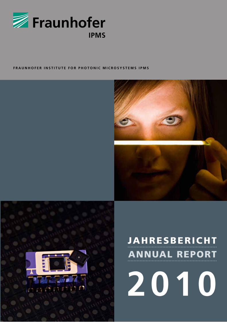
Jahresbericht
annual report
2010
F R A U N H O F E R I N S T I T U T E F O R p H O T O N I c M I c R O S y S T E M S I p M S

© Fraunhofer Institute for Photonic Microsystems IPMS,
Dresden 2011
copyrigHts
All rights reserved. Reproduction requires the permission of
the Director of the Institute.
Layout
Fraunhofer IPMS
transLation
Fraunhofer IPMS; Kathrin Muysers - Translarte, Dresden
Medienhaus Lißner OHG, Dresden
pHotos
Fraunhofer-Gesellschaft; Photographie Jürgen Lösel;
Sven Döring / VISUM; René Gaens Fotografie
© Fraunhofer-Institut für Photonische Mikrosysteme IPMS,
Dresden 2011
recHte
Alle Rechte vorbehalten. Nachdruck nur mit Genehmigung
der Institutsleitung.
gestaLtung
Fraunhofer IPMS
Übersetzung
Fraunhofer IPMS; Tara Kneitz, Dresden
druck
Medienhaus Lißner OHG, Dresden
fotos
Fraunhofer-Gesellschaft; Photographie Jürgen Lösel;
Sven Döring / VISUM; René Gaens Fotografie
impressum
editorial notes

FraunhoFer InstItute For PhotonIc
MIcrosysteMs IPMs
address: Maria-Reiche-Strasse 2,
01109 Dresden
phone: +49 (0) 3 51 / 88 23 - 0
fax: +49 (0) 3 51 / 88 23 - 2 66
e-mail: [email protected]
internet: ww.ipms.fraunhofer.de
FraunhoFer-InstItut Für PhotonIsche
MIkrosysteMe IPMs
Anschrift: Maria-Reiche-Straße 2,
01109 Dresden
Telefon: +49 (0) 3 51 / 88 23 - 0
Fax: +49 (0) 3 51 / 88 23 - 2 66
E-Mail: [email protected]
Internet: www.ipms.fraunhofer.de
2
Vorwort
Liebe Leserin, lieber Leser, liebe Freunde und Partner des
Fraunhofer-Instituts für Photonische Mikrosysteme,
im Jahr eins nach der Wirtschaftskrise zieht das Fraunhofer
IPMS eine positive Bilanz. Wir erwirtschafteten das größte
Forschungsvolumen seit Beginn unseres Bestehens - 26
Millionen Euro – und realisierten so eine Steigerung von
zwei Millionen Euro zum Vorjahr bzw. eine Verdoppelung
unseres jährlichen Forschungsbudgets in fünf Jahren.
Neben stabilen Projekten mit unseren Schlüsselkunden
und einem erneut hohen Niveau bei öffentlichen Förder-
projekten haben die signifikant gesteigerten Industrieerlöse
den größten Anteil daran. Dass wir uns in den Nachwehen
der Rezession mit guten Akquisitionserfolgen behaupten
konnten, bestätigt uns darin, dass wir weiter als attraktiver
Partner der Wirtschaft gesehen werden. Für das gezeigte
Vertrauen gilt unser besonderer Dank allen unseren Kun-
den, Fördergebern und Partnern.
Dennoch: Wer angesichts des Wachstums glaubt, wir hät-
ten die Wirtschaftsflaute rasch überwunden, liegt falsch.
Tatsächlich wurde die konjunkturelle Erholung für uns
nur langsam spürbar, und wir sahen uns veranlasst, stra-
tegische Partnerschaften auszubauen und unsere internen
Abläufe und Organisationsstrukturen weiterzuentwickeln,
um unseren Kunden noch mehr Innovation, Qualität und
Verlässlichkeit bieten zu können. Wir können sagen: 2010
war ein Jahr der Weichenstellungen:
Wir haben unser »COMEDD« - Center for Organic Materials
and Electronic Devices Dresden - als Kompetenzzentrum
neu definiert. Bislang Markenname, steht COMEDD nun für
eine eigenständige Organisation innerhalb des Fraunhofer
IPMS mit Reinraum-Infrastruktur- und Personal-Ressourcen.
Das Geschäftsmodell: Bündelung von wissenschaftlichem
Foreword
Dear Reader, Dear Friends and Partners of the Fraunhofer
Institute for Photonic Microsystems,
In the first year following the economic crisis, Fraunhofer
IMPS has drawn a positive balance. We have achieved the
largest research volume since our foundation – 26 million
euro – and as such realized an increase of two million euro
compared to last year, which is double our yearly research
budget in five years. In addition to stable projects with our
key customers and a continued high level from publicly
funded projects, the significant increase in industrial profits
has played a large part in our success. The fact that we
have been able to assert ourselves with such successful
acquisition in the aftermath of the recession attests to our
reputation as an attractive economic partner. We extend
our thanks to all of our customers, sponsors and partners
for their trust in us.
And yet: The belief that we have so quickly overcome the
recession in light of such growth is false. The recovery of
the trade cycle has been only slowly noticeable, and we
have seen the need to expand strategic partnerships and to
further develop our internal processes and organizational
structures in order to offer our clients even more innovation,
quality and dependability. We are able to say that 2010 was
a year of setting a course for the future:
We have redefined our »COMEDD« - Center for Organic
Materials and Electronic Devices Dresden – as a center of
expertise. A trade name up until recently, COMEDD now
stands for an independent organization within Fraunhofer
IPMS with clean room infrastructure and personnel re-
sources. The business model: Bundling of scientific know-
how, application experience and a client base with the goal
to put our technological expertise in the field of organic
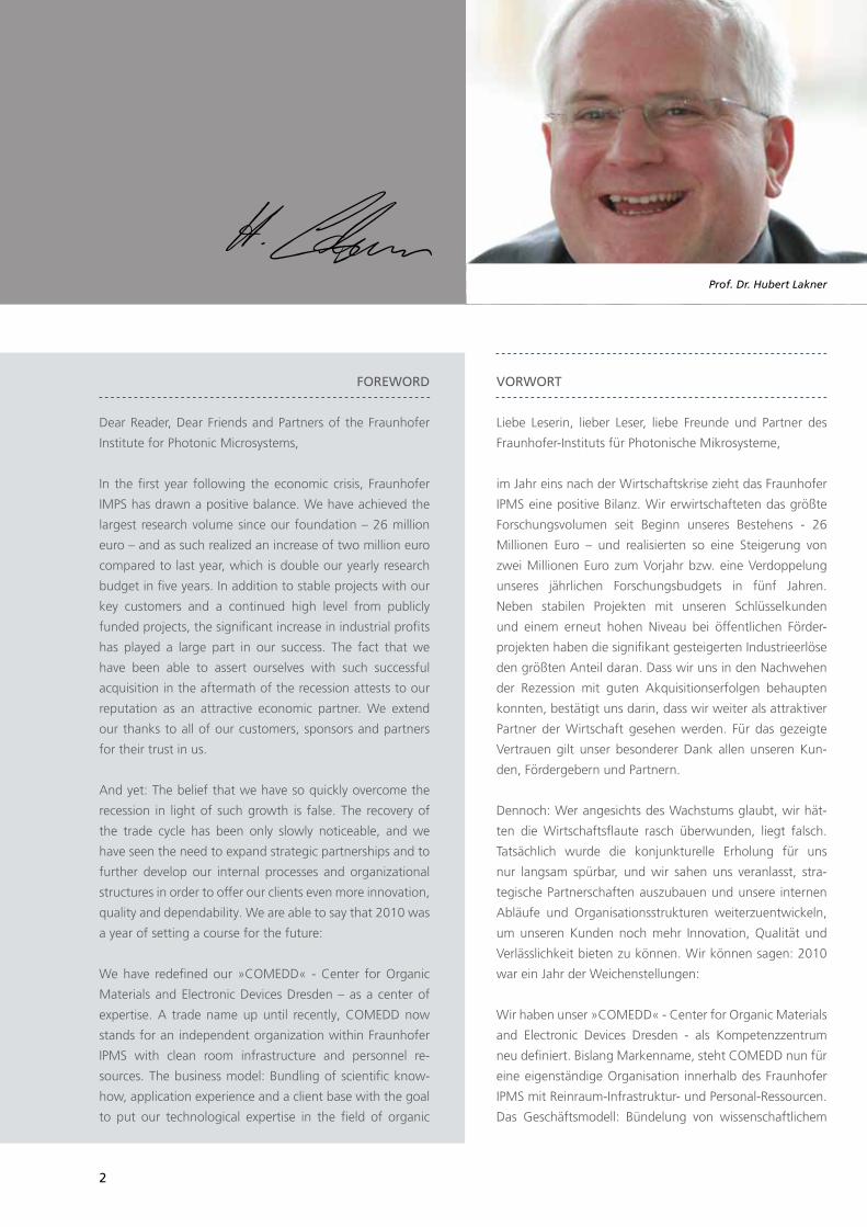
Prof. Dr. Hubert Lakner
3
electronics to industry-oriented use. Market cultivation on
the one hand and project realization in the clean room on
the other will be separated organizationally, just as they are
in silicon technology.
In the scope of microsystems technology [MEMS, MOEMS],
we have redirected business field strategies and optimized
processes in the MEMS clean room. Our customers are
already reaping the profits from measures taken to reduce
cycle times.
Last but not least, in 2010 “Lessons Learned” and mile-
stone trend analysis were established as project manage-
ment tools. We have revised the balanced score card as a
management instrument, expanded our services offered to
include standardized MEMS and OLED sample components,
and strengthened our customer service by introducing a
Customer Relationship Management (CRM) system and
employing managers to support our key clients.
All of the newly created structures and methods, as well
as the project highlights presented in this pamphlet, were
recognized by ISO 9001 recertification. We are confident
that we are internationally well-positioned and equipped
for the future due to the good reputation of our institution,
our partnerships and our unique fields of expertise.
The dedicated commitment of our team remains the pre-
requisite to our success. Our employees are highly motivated
to develop competitive products together with our clients
and to take an active role in the economic upswing. In this
regard, we look forward to meeting with you and will make
ourselves available to you at exhibitions, in scientific and
expert networks, with papers, and at personal meetings.
Know-how, Applikationserfahrung und Kundenkontakten
mit dem Ziel einer industrienahen Verwertung unserer tech-
nologischen Kompetenzen auf dem Gebiet der organischen
Elektronik. Marktbearbeitung und Projektleitung einerseits
und Projektrealisation im Reinraum andererseits sind dabei
wie bei den Siliziumtechnologien organisatorisch getrennt.
Im Kompetenzbereich der Mikrosystemtechnik [MEMS,
MOEMS] haben wir die Strategien der Geschäftsfelder neu
ausgerichtet und Abläufe im MEMS-Reinraum optimiert.
Insbesondere von Maßnahmen zur Verkürzung der Durch-
laufzeiten profitieren unsere Kunden schon heute.
Schließlich etablierten wir im Jahr 2010 „LessonsLearned“
und die Meilenstein-Trend-Analyse als Werkzeuge des
Projektmanagements, überarbeiteten die Balanced Score
Card als Managementinstrument, erweiterten unser
Leistungsangebot um standardisierte MEMS- und OLED-
Musterbauelemente und stärkten unseren Kundenservice
durch Einführung eines CRM-Systems und den Einsatz von
Managern für die Betreuung unserer Schlüsselkunden.
Alle neu gestalteten Strukturen und Methoden wie auch die
in diesem Heft präsentierten Projekt-Highlights fanden bei
der ISO 9001-Rezertifizierung Anerkennung. Wir sind über-
zeugt, dass wir mit der guten Sichtbarkeit unseres Hauses,
unseren Partnerschaften und alleinstellenden Kompetenzen
weltweit gut positioniert und für die Zukunft gerüstet sind.
Grundvoraussetzung für unseren Erfolg bleibt der enga-
gierte Einsatz unseres Teams. Unsere Mitarbeiterinnen und
Mitarbeiter sind hoch motiviert, mit Ihnen unseren Kunden
gemeinsam wettbewerbsfähige Produkte zu entwickeln und
am wirtschaftlichen Aufschwung zu partizipieren. Dafür
suchen wir Ihren Kontakt und werden auf Ausstellungen, in
Wissenschafts- und Kompetenznetzwerken, über Vorträge
und persönliche Meetings für Sie präsent sein.
Prof. Dr. Karl Leo
4
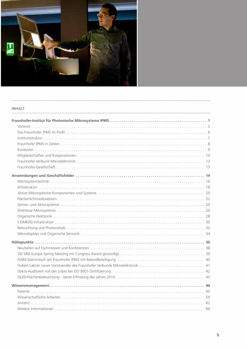
contents
Fraunhofer Institute for Photonic Microsystems IPMS . . . . . . . . . . . . . . . . . . . . . . . . . . . . . . . . . . . . . . . . . . . . . . . . . 1
Foreword . . . . . . . . . . . . . . . . . . . . . . . . . . . . . . . . . . . . . . . . . . . . . . . . . . . . . . . . . . . . . . . . . . . . . . . . . . . . . . . . . . . 2
The Fraunhofer IPMS in Profile . . . . . . . . . . . . . . . . . . . . . . . . . . . . . . . . . . . . . . . . . . . . . . . . . . . . . . . . . . . . . . . . . . . . 6
Structure of the Institute . . . . . . . . . . . . . . . . . . . . . . . . . . . . . . . . . . . . . . . . . . . . . . . . . . . . . . . . . . . . . . . . . . . . . . . . 7
Fraunhofer IPMS in Figures . . . . . . . . . . . . . . . . . . . . . . . . . . . . . . . . . . . . . . . . . . . . . . . . . . . . . . . . . . . . . . . . . . . . . . 8
Advisory Board . . . . . . . . . . . . . . . . . . . . . . . . . . . . . . . . . . . . . . . . . . . . . . . . . . . . . . . . . . . . . . . . . . . . . . . . . . . . . . . 9
Memberships and Cooperation . . . . . . . . . . . . . . . . . . . . . . . . . . . . . . . . . . . . . . . . . . . . . . . . . . . . . . . . . . . . . . . . . . 10
Fraunhofer Group for Microelectronics . . . . . . . . . . . . . . . . . . . . . . . . . . . . . . . . . . . . . . . . . . . . . . . . . . . . . . . . . . . . 12
Fraunhofer-Gesellschaft . . . . . . . . . . . . . . . . . . . . . . . . . . . . . . . . . . . . . . . . . . . . . . . . . . . . . . . . . . . . . . . . . . . . . . . . 13
Applications and Business Fields . . . . . . . . . . . . . . . . . . . . . . . . . . . . . . . . . . . . . . . . . . . . . . . . . . . . . . . . . . . . . . . . . 14
Microsystems Technology . . . . . . . . . . . . . . . . . . . . . . . . . . . . . . . . . . . . . . . . . . . . . . . . . . . . . . . . . . . . . . . . . . . . . . 16
Infrastructure . . . . . . . . . . . . . . . . . . . . . . . . . . . . . . . . . . . . . . . . . . . . . . . . . . . . . . . . . . . . . . . . . . . . . . . . . . . . . . . 18
Active Micro-optical Components and Systems . . . . . . . . . . . . . . . . . . . . . . . . . . . . . . . . . . . . . . . . . . . . . . . . . . . . . . 20
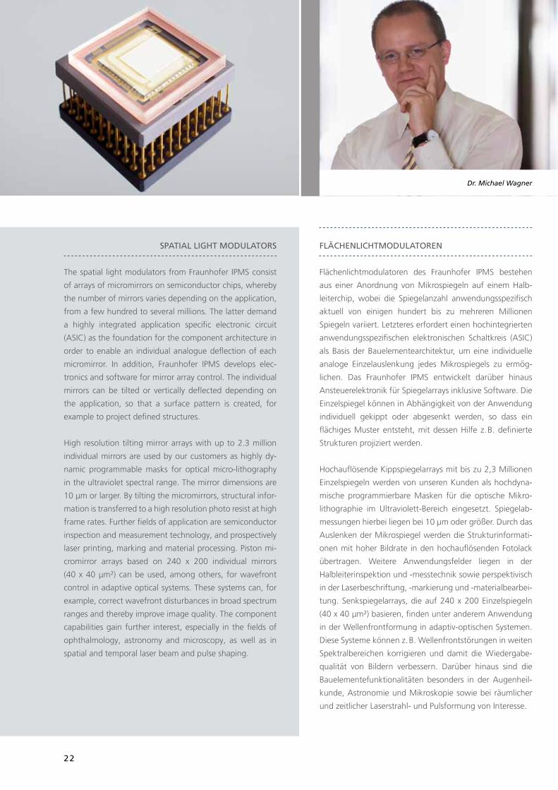
Spatial Light Modulators . . . . . . . . . . . . . . . . . . . . . . . . . . . . . . . . . . . . . . . . . . . . . . . . . . . . . . . . . . . . . . . . . . . . . . . 22
Sensor and Actuator Systems . . . . . . . . . . . . . . . . . . . . . . . . . . . . . . . . . . . . . . . . . . . . . . . . . . . . . . . . . . . . . . . . . . . 24
Wireless Microsystems . . . . . . . . . . . . . . . . . . . . . . . . . . . . . . . . . . . . . . . . . . . . . . . . . . . . . . . . . . . . . . . . . . . . . . . . . 26
Organic Electronics . . . . . . . . . . . . . . . . . . . . . . . . . . . . . . . . . . . . . . . . . . . . . . . . . . . . . . . . . . . . . . . . . . . . . . . . . . . 28
COMEDD Infrastructure . . . . . . . . . . . . . . . . . . . . . . . . . . . . . . . . . . . . . . . . . . . . . . . . . . . . . . . . . . . . . . . . . . . . . . . . 30
Lighting and Photovoltaics . . . . . . . . . . . . . . . . . . . . . . . . . . . . . . . . . . . . . . . . . . . . . . . . . . . . . . . . . . . . . . . . . . . . . . 32
Microdisplays and Organic Sensorics . . . . . . . . . . . . . . . . . . . . . . . . . . . . . . . . . . . . . . . . . . . . . . . . . . . . . . . . . . . . . . 34
Highlights . . . . . . . . . . . . . . . . . . . . . . . . . . . . . . . . . . . . . . . . . . . . . . . . . . . . . . . . . . . . . . . . . . . . . . . . . . . . . . . . . . . . 36
Innovations at Exhibitions and Conferences . . . . . . . . . . . . . . . . . . . . . . . . . . . . . . . . . . . . . . . . . . . . . . . . . . . . . . . . . 38
SID MID Europe Spring Meeting Honored with Convention Award . . . . . . . . . . . . . . . . . . . . . . . . . . . . . . . . . . . . . . . 39
Record Attendance for IVAM Gathering at Fraunhofer IPMS . . . . . . . . . . . . . . . . . . . . . . . . . . . . . . . . . . . . . . . . . . . . 40
Hubert Lakner is the New Chairman of the Fraunhofer Group for Microelectronics . . . . . . . . . . . . . . . . . . . . . . . . . . . 41
DEKRA Auditors Full of Praise for ISO 9001 Certification . . . . . . . . . . . . . . . . . . . . . . . . . . . . . . . . . . . . . . . . . . . . . . . 42
OLED Large Area Lighting – Best Invention of 2010 . . . . . . . . . . . . . . . . . . . . . . . . . . . . . . . . . . . . . . . . . . . . . . . . . . 43
Knowledge Management . . . . . . . . . . . . . . . . . . . . . . . . . . . . . . . . . . . . . . . . . . . . . . . . . . . . . . . . . . . . . . . . . . . . . . . 44
Patents . . . . . . . . . . . . . . . . . . . . . . . . . . . . . . . . . . . . . . . . . . . . . . . . . . . . . . . . . . . . . . . . . . . . . . . . . . . . . . . . . . . . 45
Academic Theses . . . . . . . . . . . . . . . . . . . . . . . . . . . . . . . . . . . . . . . . . . . . . . . . . . . . . . . . . . . . . . . . . . . . . . . . . . . . . 59
How to reach us . . . . . . . . . . . . . . . . . . . . . . . . . . . . . . . . . . . . . . . . . . . . . . . . . . . . . . . . . . . . . . . . . . . . . . . . . . . . . 62
More Information . . . . . . . . . . . . . . . . . . . . . . . . . . . . . . . . . . . . . . . . . . . . . . . . . . . . . . . . . . . . . . . . . . . . . . . . . . . . 64
5
Inhalt
Fraunhofer-Institut für Photonische Mikrosysteme IPMS . . . . . . . . . . . . . . . . . . . . . . . . . . . . . . . . . . . . . . . . . . . . . . . 1
Vorwort . . . . . . . . . . . . . . . . . . . . . . . . . . . . . . . . . . . . . . . . . . . . . . . . . . . . . . . . . . . . . . . . . . . . . . . . . . . . . . . . . . . . . 2
Das Fraunhofer IPMS im Profil . . . . . . . . . . . . . . . . . . . . . . . . . . . . . . . . . . . . . . . . . . . . . . . . . . . . . . . . . . . . . . . . . . . . 6
Institutsstruktur . . . . . . . . . . . . . . . . . . . . . . . . . . . . . . . . . . . . . . . . . . . . . . . . . . . . . . . . . . . . . . . . . . . . . . . . . . . . . . . 7
Fraunhofer IPMS in Zahlen . . . . . . . . . . . . . . . . . . . . . . . . . . . . . . . . . . . . . . . . . . . . . . . . . . . . . . . . . . . . . . . . . . . . . . . 8
Kuratoren . . . . . . . . . . . . . . . . . . . . . . . . . . . . . . . . . . . . . . . . . . . . . . . . . . . . . . . . . . . . . . . . . . . . . . . . . . . . . . . . . . . 9
Mitgliedschaften und Kooperationen . . . . . . . . . . . . . . . . . . . . . . . . . . . . . . . . . . . . . . . . . . . . . . . . . . . . . . . . . . . . . . 10
Fraunhofer-Verbund Mikroelektronik . . . . . . . . . . . . . . . . . . . . . . . . . . . . . . . . . . . . . . . . . . . . . . . . . . . . . . . . . . . . . . 12
Fraunhofer-Gesellschaft . . . . . . . . . . . . . . . . . . . . . . . . . . . . . . . . . . . . . . . . . . . . . . . . . . . . . . . . . . . . . . . . . . . . . . . . 13
Anwendungen und Geschäftsfelder . . . . . . . . . . . . . . . . . . . . . . . . . . . . . . . . . . . . . . . . . . . . . . . . . . . . . . . . . . . . . . 14
Mikrosystemtechnik . . . . . . . . . . . . . . . . . . . . . . . . . . . . . . . . . . . . . . . . . . . . . . . . . . . . . . . . . . . . . . . . . . . . . . . . . . 16
Infrastruktur . . . . . . . . . . . . . . . . . . . . . . . . . . . . . . . . . . . . . . . . . . . . . . . . . . . . . . . . . . . . . . . . . . . . . . . . . . . . . . . . 18
Aktive Mikrooptische Komponenten und Systeme . . . . . . . . . . . . . . . . . . . . . . . . . . . . . . . . . . . . . . . . . . . . . . . . . . . 20
Flächenlichtmodulatoren . . . . . . . . . . . . . . . . . . . . . . . . . . . . . . . . . . . . . . . . . . . . . . . . . . . . . . . . . . . . . . . . . . . . . . . 22
Sensor- und Aktorsysteme . . . . . . . . . . . . . . . . . . . . . . . . . . . . . . . . . . . . . . . . . . . . . . . . . . . . . . . . . . . . . . . . . . . . . . 24
Drahtlose Mikrosysteme . . . . . . . . . . . . . . . . . . . . . . . . . . . . . . . . . . . . . . . . . . . . . . . . . . . . . . . . . . . . . . . . . . . . . . . 26
Organische Elektronik . . . . . . . . . . . . . . . . . . . . . . . . . . . . . . . . . . . . . . . . . . . . . . . . . . . . . . . . . . . . . . . . . . . . . . . . . 28
COMEDD Infrastruktur . . . . . . . . . . . . . . . . . . . . . . . . . . . . . . . . . . . . . . . . . . . . . . . . . . . . . . . . . . . . . . . . . . . . . . . . 30
Beleuchtung und Photovoltaik . . . . . . . . . . . . . . . . . . . . . . . . . . . . . . . . . . . . . . . . . . . . . . . . . . . . . . . . . . . . . . . . . . . 32
Mikrodisplays und Organische Sensorik . . . . . . . . . . . . . . . . . . . . . . . . . . . . . . . . . . . . . . . . . . . . . . . . . . . . . . . . . . . . 34
Höhepunkte . . . . . . . . . . . . . . . . . . . . . . . . . . . . . . . . . . . . . . . . . . . . . . . . . . . . . . . . . . . . . . . . . . . . . . . . . . . . . . . . . . 36
Neuheiten auf Fachmessen und Konferenzen . . . . . . . . . . . . . . . . . . . . . . . . . . . . . . . . . . . . . . . . . . . . . . . . . . . . . . . 38
SID MID Europe Spring Meeting mit Congress Award gewürdigt . . . . . . . . . . . . . . . . . . . . . . . . . . . . . . . . . . . . . . . . . 39
IVAM-Stammtisch am Fraunhofer IPMS mit Rekordbeteiligung . . . . . . . . . . . . . . . . . . . . . . . . . . . . . . . . . . . . . . . . . . 40
Hubert Lakner neuer Vorsitzender des Fraunhofer Verbunds Mikroelektronik . . . . . . . . . . . . . . . . . . . . . . . . . . . . . . . . 41
Dekra-Auditoren voll des Lobes bei ISO 9001-Zertifizierung . . . . . . . . . . . . . . . . . . . . . . . . . . . . . . . . . . . . . . . . . . . . . 42
OLED-Flächenbeleuchtung – beste Erfindung des Jahres 2010 . . . . . . . . . . . . . . . . . . . . . . . . . . . . . . . . . . . . . . . . . . . 43
Wissensmanagement . . . . . . . . . . . . . . . . . . . . . . . . . . . . . . . . . . . . . . . . . . . . . . . . . . . . . . . . . . . . . . . . . . . . . . . . . . . 44
Patente . . . . . . . . . . . . . . . . . . . . . . . . . . . . . . . . . . . . . . . . . . . . . . . . . . . . . . . . . . . . . . . . . . . . . . . . . . . . . . . . . . . . 45
Wissenschaftliche Arbeiten . . . . . . . . . . . . . . . . . . . . . . . . . . . . . . . . . . . . . . . . . . . . . . . . . . . . . . . . . . . . . . . . . . . . . 59
Anfahrt . . . . . . . . . . . . . . . . . . . . . . . . . . . . . . . . . . . . . . . . . . . . . . . . . . . . . . . . . . . . . . . . . . . . . . . . . . . . . . . . . . . . 62
Weitere Informationen . . . . . . . . . . . . . . . . . . . . . . . . . . . . . . . . . . . . . . . . . . . . . . . . . . . . . . . . . . . . . . . . . . . . . . . . 64
6
das FraunhoFer IPMs IM ProFIl
Das Fraunhofer-Institut für Photonische Mikrosysteme
IPMS realisiert mit 220 Mitarbeiterinnen und Mitarbeitern
ein jährliches Forschungsvolumen von nahezu 26 Millio-
nen Euro. Mehr als zwei Drittel dieses Leistungsbereichs
erwirtschaftet das Fraunhofer IPMS mit Aufträgen aus der
Wirtschaft und mit öffentlich finanzierten Projekten der
angewandten Forschung.
Im Fokus der Entwicklungs- und Fertigungsleistungen
steht die industrienahe Verwertung der alleinstellenden
technologischen Kompetenzen auf den Gebieten der
(optischen) Mikro-Elektromechanischen Systeme [MEMS,
MOEMS] einerseits und der Organischen Elektronik [OLED,
organische Photovoltaik] andererseits. Dabei bündelt das
Fraunhofer IPMS wissenschaftliches Know-how, Applikati-
onserfahrung und Kundenkontakte beider Forschungsrich-
tungen in den Kompetenzentren »Mikrosystemtechnik«
und »COMEDD« – Center for Organic Materials and
Electronic Devices Dresden mit eigenständigen Reinraum-
Infrastruktur- und Personal-Ressourcen.
Das Fraunhofer IPMS deckt eine breite Palette industrieller
Anwendungen ab. Das Leistungsangebot reicht von der
Konzeption über die Produktentwicklung bis zur Pilotseri-
enfertigung – vom Bauelement bis zur kompletten System-
lösung.
the FraunhoFer IPMs In ProFIle
The Fraunhofer Institute for Photonic Microsystems IPMS
and its 220 employees turn over an annual research volume
of nearly 26 million euros. Fraunhofer IPMS generates more
than two thirds of this production capacity out of commis-
sions from industry and publicly financed projects in applied
research.
The focus of our development and production services lies in
the practical industrial application of unique technological
know-how in the fields of (optical) micro-electromechanical
systems [MEMS, MOEMS] on the one hand, and organic
electronics [OLED, organic photovoltaics] on the other.
Fraunhofer IMPS combines scientific know-how, applica-
tion experience and customer contacts from both research
branches in its centers for expertise “Microsystems technol-
ogy” and “COMEDD” – Center for Organic Materials and
Electronic Devices Dresden with independent clean room
infrastructure and personnel resources.
Fraunhofer IPMS covers a broad spectrum of industrial
applications. Our services range from initial conception to
product development, right down to serial pilot produc-
tion – from a single component to a complete system
solution.
7
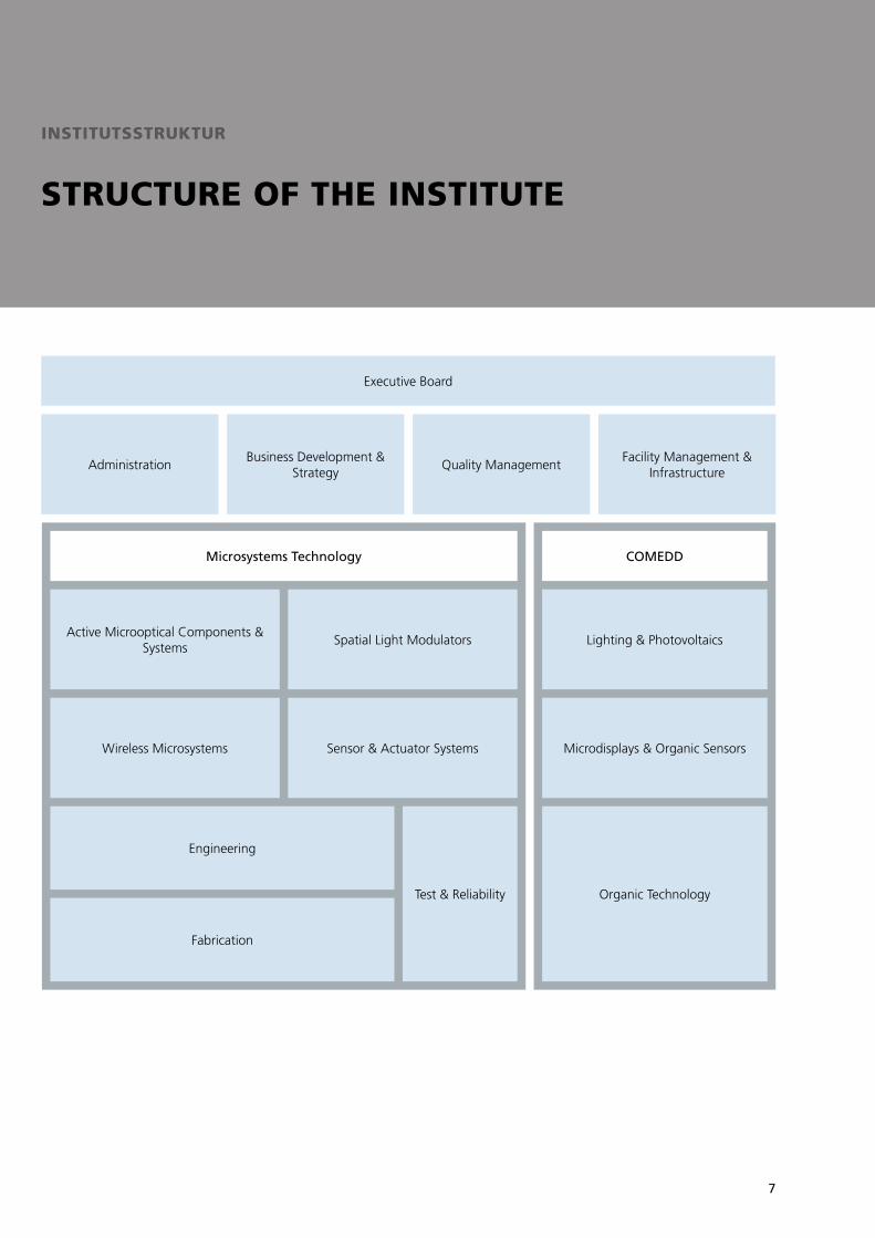
InstItutsstruktur
structure of the InstItute
Executive Board
AdministrationBusiness Development &
StrategyQuality Management
Facility Management & Infrastructure
Organic TechnologyTest & Reliability
Engineering
Fabrication
Active Microoptical Components & Systems
Spatial Light Modulators
Wireless Microsystems Sensor & Actuator Systems
Lighting & Photovoltaics
Microdisplays & Organic Sensors
Microsystems technology coMedd
8
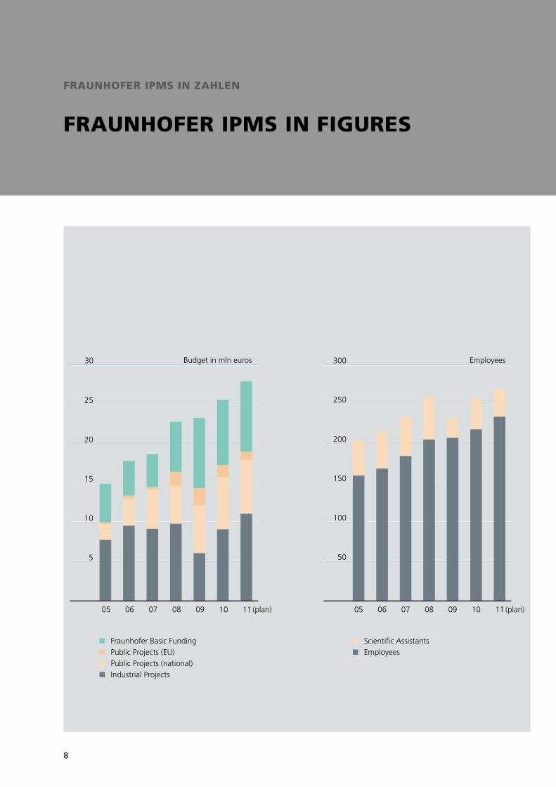
fraunhofer IPMs In Zahlen
fraunhofer IPMs In fIgures
Fraunhofer Basic FundingPublic Projects (EU)Public Projects (national)Industrial Projects
5
10
15
20
25
30
11100908070605
Budget in mln euros
50
100
150
200
250
300
11100908070605
Employees
Scientific AssistantsEmployees
(plan) (plan)
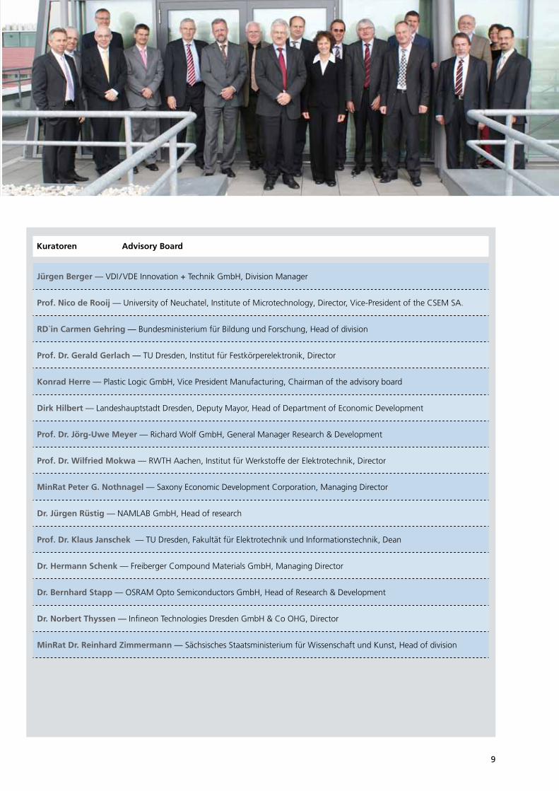
kuratoren
advIsory Board
9
Kuratoren Advisory Board
Jürgen Berger — VDI / VDE Innovation + Technik GmbH, Division Manager
Prof . Nico de Rooij — University of Neuchatel, Institute of Microtechnology, Director, Vice-President of the CSEM SA.
RD`in Carmen Gehring — Bundesministerium für Bildung und Forschung, Head of division
Prof . Dr . Gerald Gerlach — TU Dresden, Institut für Festkörperelektronik, Director
Konrad Herre — Plastic Logic GmbH, Vice President Manufacturing, Chairman of the advisory board
Dirk Hilbert — Landeshauptstadt Dresden, Deputy Mayor, Head of Department of Economic Development
Prof . Dr . Jörg-Uwe Meyer — Richard Wolf GmbH, General Manager Research & Development
Prof . Dr . Wilfried Mokwa — RWTH Aachen, Institut für Werkstoffe der Elektrotechnik, Director
MinRat Peter G . Nothnagel — Saxony Economic Development Corporation, Managing Director
Dr . Jürgen Rüstig — NAMLAB GmbH, Head of research
Prof . Dr . Klaus Janschek — TU Dresden, Fakultät für Elektrotechnik und Informationstechnik, Dean
Dr . Hermann Schenk — Freiberger Compound Materials GmbH, Managing Director
Dr . Bernhard Stapp — OSRAM Opto Semiconductors GmbH, Head of Research & Development
Dr . Norbert Thyssen — Infineon Technologies Dresden GmbH & Co OHG, Director
MinRat Dr . Reinhard Zimmermann — Sächsisches Staatsministerium für Wissenschaft und Kunst, Head of division
10
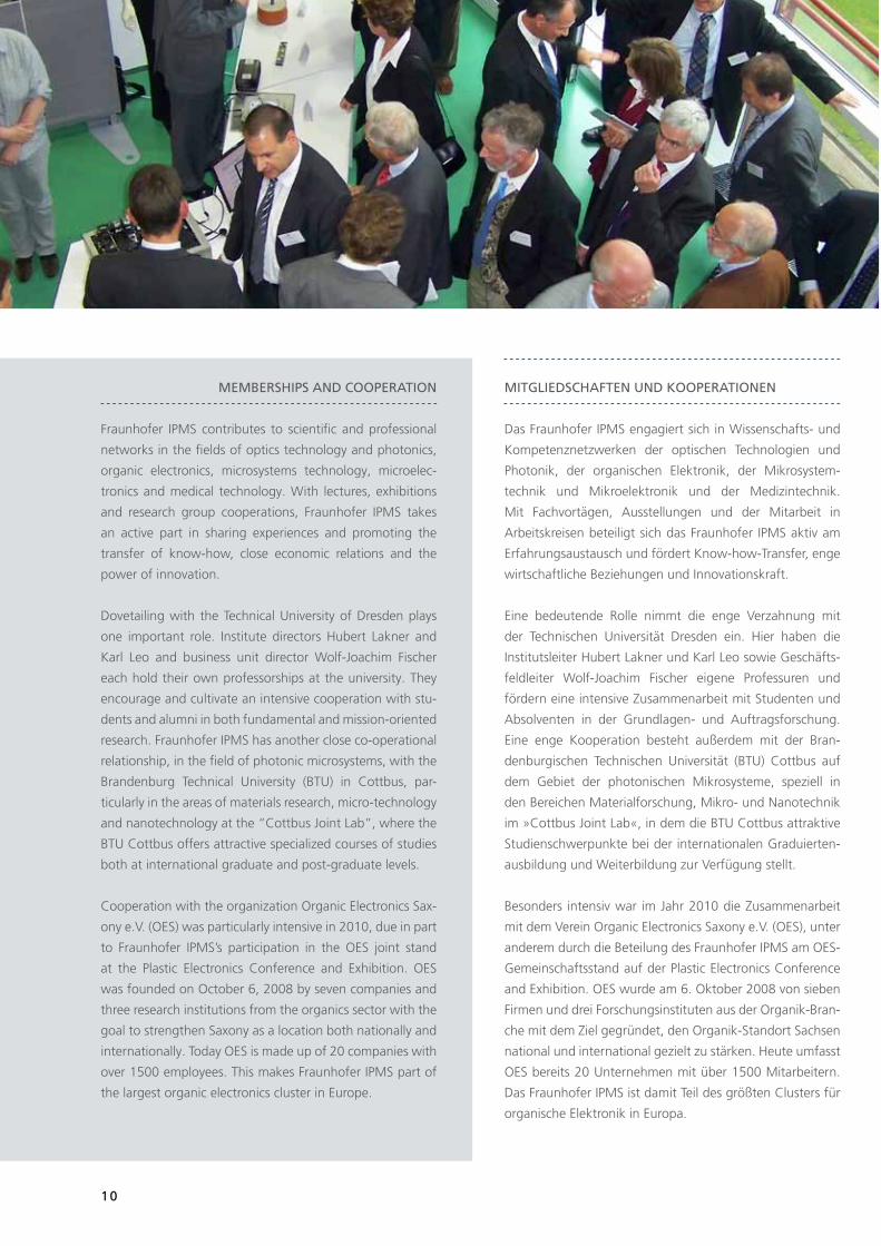
MeMbershIPs and cooPeratIon
Fraunhofer IPMS contributes to scientific and professional
networks in the fields of optics technology and photonics,
organic electronics, microsystems technology, microelec-
tronics and medical technology. With lectures, exhibitions
and research group cooperations, Fraunhofer IPMS takes
an active part in sharing experiences and promoting the
transfer of know-how, close economic relations and the
power of innovation.
Dovetailing with the Technical University of Dresden plays
one important role. Institute directors Hubert Lakner and
Karl Leo and business unit director Wolf-Joachim Fischer
each hold their own professorships at the university. They
encourage and cultivate an intensive cooperation with stu-
dents and alumni in both fundamental and mission-oriented
research. Fraunhofer IPMS has another close co-operational
relationship, in the field of photonic microsystems, with the
Brandenburg Technical University (BTU) in Cottbus, par-
ticularly in the areas of materials research, micro-technology
and nanotechnology at the “Cottbus Joint Lab”, where the
BTU Cottbus offers attractive specialized courses of studies
both at international graduate and post-graduate levels.
Cooperation with the organization Organic Electronics Sax-
ony e.V. (OES) was particularly intensive in 2010, due in part
to Fraunhofer IPMS’s participation in the OES joint stand
at the Plastic Electronics Conference and Exhibition. OES
was founded on October 6, 2008 by seven companies and
three research institutions from the organics sector with the
goal to strengthen Saxony as a location both nationally and
internationally. Today OES is made up of 20 companies with
over 1500 employees. This makes Fraunhofer IPMS part of
the largest organic electronics cluster in Europe.
MItglIedschaFten und kooPeratIonen
Das Fraunhofer IPMS engagiert sich in Wissenschafts- und
Kompetenznetzwerken der optischen Technologien und
Photonik, der organischen Elektronik, der Mikrosystem-
technik und Mikroelektronik und der Medizintechnik.
Mit Fachvortägen, Ausstellungen und der Mitarbeit in
Arbeitskreisen beteiligt sich das Fraunhofer IPMS aktiv am
Erfahrungsaustausch und fördert Know-how-Transfer, enge
wirtschaftliche Beziehungen und Innovationskraft.
Eine bedeutende Rolle nimmt die enge Verzahnung mit
der Technischen Universität Dresden ein. Hier haben die
Institutsleiter Hubert Lakner und Karl Leo sowie Geschäfts-
feldleiter Wolf-Joachim Fischer eigene Professuren und
fördern eine intensive Zusammenarbeit mit Studenten und
Absolventen in der Grundlagen- und Auftragsforschung.
Eine enge Kooperation besteht außerdem mit der Bran-
denburgischen Technischen Universität (BTU) Cottbus auf
dem Gebiet der photonischen Mikrosysteme, speziell in
den Bereichen Materialforschung, Mikro- und Nanotechnik
im »Cottbus Joint Lab«, in dem die BTU Cottbus attraktive
Studienschwerpunkte bei der internationalen Graduierten-
ausbildung und Weiterbildung zur Verfügung stellt.
Besonders intensiv war im Jahr 2010 die Zusammenarbeit
mit dem Verein Organic Electronics Saxony e.V. (OES), unter
anderem durch die Beteilung des Fraunhofer IPMS am OES-
Gemeinschaftsstand auf der Plastic Electronics Conference
and Exhibition. OES wurde am 6. Oktober 2008 von sieben
Firmen und drei Forschungsinstituten aus der Organik-Bran-
che mit dem Ziel gegründet, den Organik-Standort Sachsen
national und international gezielt zu stärken. Heute umfasst
OES bereits 20 Unternehmen mit über 1500 Mitarbeitern.
Das Fraunhofer IPMS ist damit Teil des größten Clusters für
organische Elektronik in Europa.
11
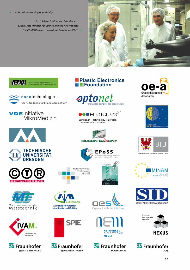
e Informal networking opportunity
Prof. Sabine Freifrau von Schorlemer ,
Saxon State Minister for Science and the Arts inspects
the COMEDD clean room of the Fraunhofer IPMS
HeterogeneousTechnology
Alliance
Deutsche Forschungsgesellschaft fürAutomatisierung und Mikroelektronik e.V.
SOCIETY FOR INFORMATION DISPLAY
Fachverband fürMikrotechnik
M.IVA
DEUTSCHLAND e.V.
EuropeanMicrosystemsNetwork
European Technology Platform“Photonics for the 21st Century“
InitiativeMikroMedizin
Plastic ElectronicsFoundation
Micro- andNanoManufacturing
MINAM
12
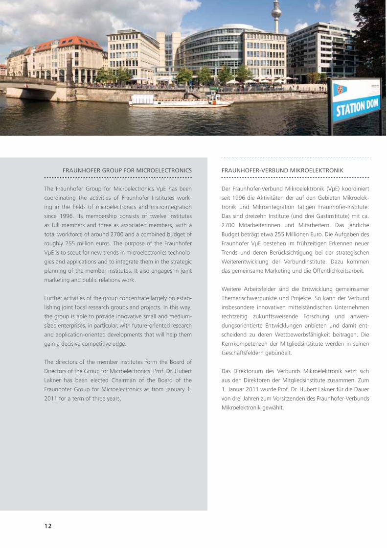
FraunhoFer grouP For MIcroelectronIcs
The Fraunhofer Group for Microelectronics VµE has been
coordinating the activities of Fraunhofer Institutes work-
ing in the fields of microelectronics and microintegration
since 1996. Its membership consists of twelve institutes
as full members and three as associated members, with a
total workforce of around 2700 and a combined budget of
roughly 255 million euros. The purpose of the Fraunhofer
VµE is to scout for new trends in microelectronics technolo-
gies and applications and to integrate them in the strategic
planning of the member institutes. It also engages in joint
marketing and public relations work.
Further activities of the group concentrate largely on estab-
lishing joint focal research groups and projects. In this way,
the group is able to provide innovative small and medium-
sized enterprises, in particular, with future-oriented research
and application-oriented developments that will help them
gain a decisive competitive edge.
The directors of the member institutes form the Board of
Directors of the Group for Microelectronics. Prof. Dr. Hubert
Lakner has been elected Chairman of the Board of the
Fraunhofer Group for Microelectronics as from January 1,
2011 for a term of three years.
FraunhoFer-Verbund MIkroelektronIk
Der Fraunhofer-Verbund Mikroelektronik (VµE) koordiniert
seit 1996 die Aktivitäten der auf den Gebieten Mikroelek-
tronik und Mikrointegration tätigen Fraunhofer-Institute:
Das sind dreizehn Institute (und drei Gastinstitute) mit ca.
2700 Mitarbeiterinnen und Mitarbeitern. Das jährliche
Budget beträgt etwa 255 Millionen Euro. Die Aufgaben des
Fraunhofer VµE bestehen im frühzeitigen Erkennen neuer
Trends und deren Berücksichtigung bei der strategischen
Weiterentwicklung der Verbundinstitute. Dazu kommen
das gemeinsame Marketing und die Öffentlichkeitsarbeit.
Weitere Arbeitsfelder sind die Entwicklung gemeinsamer
Themenschwerpunkte und Projekte. So kann der Verbund
insbesondere innovativen mittelständischen Unternehmen
rechtzeitig zukunftsweisende Forschung und anwen-
dungsorientierte Entwicklungen anbieten und damit ent-
scheidend zu deren Wettbewerbsfähigkeit beitragen. Die
Kernkompetenzen der Mitgliedsinstitute werden in seinen
Geschäftsfeldern gebündelt.
Das Direktorium des Verbunds Mikroelektronik setzt sich
aus den Direktoren der Mitgliedsinstitute zusammen. Zum
1. Januar 2011 wurde Prof. Dr. Hubert Lakner für die Dauer
von drei Jahren zum Vorsitzenden des Fraunhofer-Verbunds
Mikroelektronik gewählt.
13
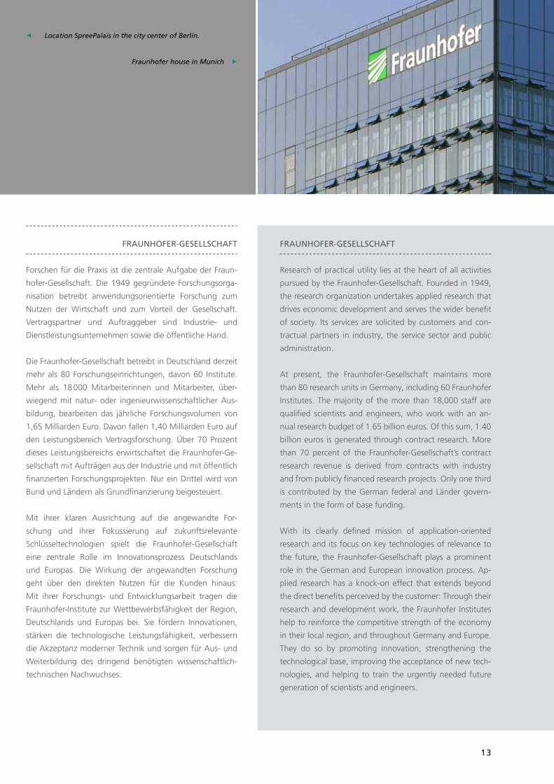
e Location SpreePalais in the city center of Berlin.
Fraunhofer house in Munich
FraunhoFer-gesellschaFt
Research of practical utility lies at the heart of all activities
pursued by the Fraunhofer-Gesellschaft. Founded in 1949,
the research organization undertakes applied research that
drives economic development and serves the wider benefit
of society. Its services are solicited by customers and con-
tractual partners in industry, the service sector and public
administration.
At present, the Fraunhofer-Gesellschaft maintains more
than 80 research units in Germany, including 60 Fraunhofer
Institutes. The majority of the more than 18,000 staff are
qualified scientists and engineers, who work with an an-
nual research budget of 1.65 billion euros. Of this sum, 1.40
billion euros is generated through contract research. More
than 70 percent of the Fraunhofer-Gesellschaft’s contract
research revenue is derived from contracts with industry
and from publicly financed research projects. Only one third
is contributed by the German federal and Länder govern-
ments in the form of base funding.
With its clearly defined mission of application-oriented
research and its focus on key technologies of relevance to
the future, the Fraunhofer-Gesellschaft plays a prominent
role in the German and European innovation process. Ap-
plied research has a knock-on effect that extends beyond
the direct benefits perceived by the customer: Through their
research and development work, the Fraunhofer Institutes
help to reinforce the competitive strength of the economy
in their local region, and throughout Germany and Europe.
They do so by promoting innovation, strengthening the
technological base, improving the acceptance of new tech-
nologies, and helping to train the urgently needed future
generation of scientists and engineers.
FraunhoFer-gesellschaFt
Forschen für die Praxis ist die zentrale Aufgabe der Fraun-
hofer-Gesellschaft. Die 1949 gegründete Forschungsorga-
nisation betreibt anwendungsorientierte Forschung zum
Nutzen der Wirtschaft und zum Vorteil der Gesellschaft.
Vertragspartner und Auftraggeber sind Industrie- und
Dienstleistungsunternehmen sowie die öffentliche Hand.
Die Fraunhofer-Gesellschaft betreibt in Deutschland derzeit
mehr als 80 Forschungseinrichtungen, davon 60 Institute.
Mehr als 18 000 Mitarbeiterinnen und Mitarbeiter, über-
wiegend mit natur- oder ingenieurwissenschaftlicher Aus-
bildung, bearbeiten das jährliche Forschungsvolumen von
1,65 Milliarden Euro. Davon fallen 1,40 Milliarden Euro auf
den Leistungsbereich Vertragsforschung. Über 70 Prozent
dieses Leistungsbereichs erwirtschaftet die Fraunhofer-Ge-
sellschaft mit Aufträgen aus der Industrie und mit öffentlich
finanzierten Forschungsprojekten. Nur ein Drittel wird von
Bund und Ländern als Grundfinanzierung beigesteuert.
Mit ihrer klaren Ausrichtung auf die angewandte For-
schung und ihrer Fokussierung auf zukunftsrelevante
Schlüsseltechnologien spielt die Fraunhofer-Gesellschaft
eine zentrale Rolle im Innovationsprozess Deutschlands
und Europas. Die Wirkung der angewandten Forschung
geht über den direkten Nutzen für die Kunden hinaus:
Mit ihrer Forschungs- und Entwicklungsarbeit tragen die
Fraunhofer-Institute zur Wettbewerbsfähigkeit der Region,
Deutschlands und Europas bei. Sie fördern Innovationen,
stärken die technologische Leistungsfähigkeit, verbessern
die Akzeptanz moderner Technik und sorgen für Aus- und
Weiterbildung des dringend benötigten wissenschaftlich-
technischen Nachwuchses.

anwendungen und geschäftsfelder
aPPlIcatIons and BusIness fIelds
16
MIkrosysteMtechnIk
MIcrosysteMs technology
17
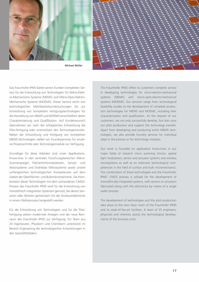
The Fraunhofer IPMS offers its customers complete service
in developing technologies for micro-electro-mechanical
systems (MEMS) and micro-opto-electro-mechanical
systems (MOEMS). Our services range from technological
feasibility studies to the development of complete produc-
tion technologies for MEMS and MOEMS, including their
characterization and qualification. At the request of our
customers, we not only successfully develop, but also carry
out pilot production and support the technology transfer.
Apart from developing and producing entire MEMS tech-
nologies, we also provide foundry services for individual
steps in the process or for technology modules.
Our work is founded on application know-how in our
major fields of research micro scanning mirrors, spatial
light modulators, sensor and actuator systems and wireless
microsystems as well as on extensive technological com-
petencies in the field of surface and bulk micromechanics.
The combination of these technologies and the Fraunhofer
IPMS’ CMOS process is utilized for the development of
monolithically integrated systems, with sensors or actuators
fabricated along with the electronics by means of a single
wafer process.
The development of technologies and the pilot production
take place at the new clean room of the Fraunhofer IPMS
and its state-of-the-art facilities. A team of 25 engineers,
physicists and chemists assists the technological develop-
ments of the business units.
Das Fraunhofer IPMS bietet seinen Kunden kompletten Ser-
vice für die Entwicklung von Technologien für Mikro-Elekt-
ro-Mechanische Systeme (MEMS) und Mikro-Opto-Elektro-
Mechanische Systeme (MOEMS). Dieser Service reicht von
technologischen Machbarkeitsuntersuchungen bis zur
Entwicklung von kompletten Fertigungstechnologien für
die Herstellung von MEMS und MOEMS einschließlich deren
Charakterisierung und Qualifikation. Auf Kundenwunsch
übernehmen wir nach der erfolgreichen Entwicklung die
Pilot-Fertigung oder unterstützen den Technologietransfer.
Neben der Entwicklung und Fertigung von kompletten
MEMS-Technologien stellen wir Foundryservices für einzel-
ne Prozessschritte oder Technologiemodule zur Verfügung.
Grundlage für diese Arbeiten sind unser Applikations-
Know-how in den zentralen Forschungsbereichen Mikro-
Scannerspiegel, Flächenlichtmodulatoren, Sensor- und
Aktorsysteme und Drahtlose Mikrosysteme sowie unsere
umfangreichen technologischen Kompetenzen auf dem
Gebiet der Oberflächen- und Bulkmikromechanik. Die Kom-
bination dieser Technologien mit dem vorhandenen CMOS-
Prozess des Fraunhofer IPMS wird für die Entwicklung von
monolithisch integrierten Systemen genutzt, bei denen Sen-
soren oder Aktoren gemeinsam mit der Ansteuer elektronik
in einem Waferprozess hergestellt werden.
Für die Entwicklung von Technologien und für die Pilot-
Fertigung stehen modernste Anlagen und der neue Rein-
raum des Fraunhofer IPMS zur Verfügung. Ein Team aus
25 Ingenieuren, Physikern und Chemikern unterstützt im
Bereich Engineering die technologischen Entwicklungen in
den Geschäftsfeldern.
Michael Müller
18
InFrastruktur
Mit der Inbetriebnahme des MEMS-Reinraums – Klasse ISO2
nach 14644-1 (10 nach 209E) – im September 2007 stehen
dem Fraunhofer IPMS auf 1500 m² nahezu unbegrenzte
Möglichkeiten zur Verfügung, um Forschung und Entwick-
lung an photonischen Mikrosystemen voranzutreiben.
Mit dieser von der Europäischen Union, Bund, Land Sachsen
und Fraunhofer-Gesellschaft geförderten Investition ist es
uns möglich geworden, von der Idee über die Lösungs-
findung bis hin zur Pilot-Fertigung den Wünschen unserer
Kunden gerecht zu werden. Dabei sind wir für vielfältigste
Kooperationsmodelle offen, angefangen von der komplet-
ten Forschung und Entwicklung über gemeinschaftliche
Projektarbeit einschließlich der Nutzung unserer Infrastruk-
tur und Anlagentechnik durch unsere Auftraggeber bis hin
zu Foundry-Dienstleistungen für einzelne Prozessschritte
oder komplette Produktfertigung.
Die Fertigungsleistungen umfassen Waferpräparation, Auf-
bau- und Verbindungstechnik sowie die Organisation von
externen Dienst- und Zulieferleistungen. Zur Absicherung
einer effizienten Präparation vom Wafer über den Chip bis
zum System stehen die Instandhaltungsgruppe für die War-
tung und Reparatur der Ausrüstungen, die Fertigungspla-
nung und -steuerung für eine durchgehend termingerechte
Abarbeitung sowie die Prozesssteuerung zur Sicherstellung
einer stabilen Prozesssierung zur Verfügung.
Das offene Konzept des Reinraumes erlaubt Planungen,
die auch künftigen technologischen Entwicklungen und
Maschinengenerationen gerecht werden. Der Reinraum
wurde nach modernsten Industriestandards geplant und
errichtet. Seine vernetzten Sicherheitssysteme ermöglichen
ein Höchstmaß an Schutz für Menschen und Umwelt.
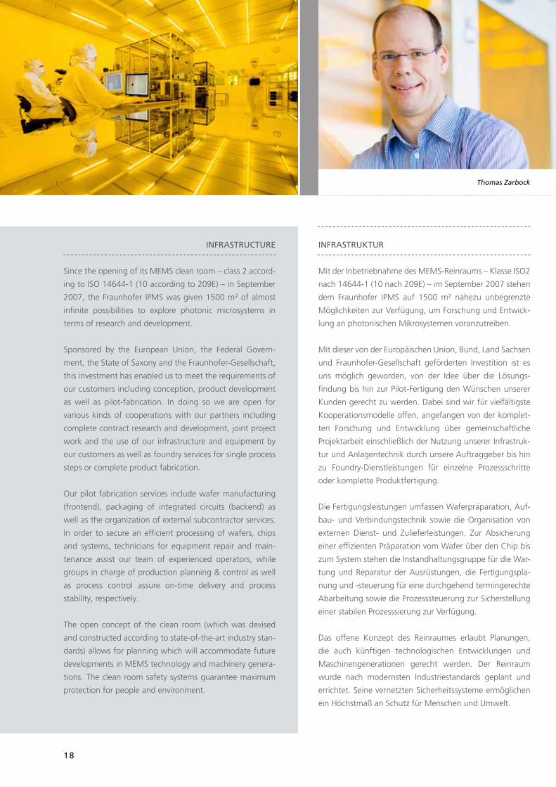
InFrastructure
Since the opening of its MEMS clean room – class 2 accord-
ing to ISO 14644-1 (10 according to 209E) – in September
2007, the Fraunhofer IPMS was given 1500 m² of almost
infinite possibilities to explore photonic microsystems in
terms of research and development.
Sponsored by the European Union, the Federal Govern-
ment, the State of Saxony and the Fraunhofer-Gesellschaft,
this investment has enabled us to meet the requirements of
our customers including conception, product development
as well as pilot-fabrication. In doing so we are open for
various kinds of cooperations with our partners including
complete contract research and development, joint project
work and the use of our infrastructure and equipment by
our customers as well as foundry services for single process
steps or complete product fabrication.
Our pilot fabrication services include wafer manufacturing
(frontend), packaging of integrated circuits (backend) as
well as the organization of external subcontractor services.
In order to secure an efficient processing of wafers, chips
and systems, technicians for equipment repair and main-
tenance assist our team of experienced operators, while
groups in charge of production planning & control as well
as process control assure on-time delivery and process
stability, respectively.
The open concept of the clean room (which was devised
and constructed according to state-of-the-art industry stan-
dards) allows for planning which will accommodate future
developments in MEMS technology and machinery genera-
tions. The clean room safety systems guarantee maximum
protection for people and environment.
Thomas Zarbock
19
headIng
Text
überschrIFt
Text
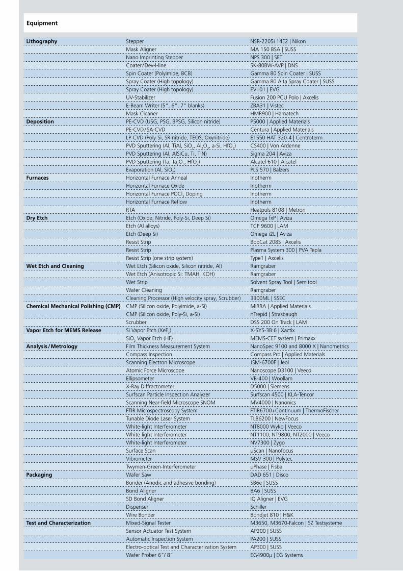
Lithography Stepper NSR-2205i 14E2 | Nikon
Mask Aligner MA 150 BSA | SUSS
Nano Imprinting Stepper NPS 300 | SET
Coater / Dev-l-line SK-80BW-AVP | DNS
Spin Coater (Polyimide, BCB) Gamma 80 Spin Coater | SUSS
Spray Coater (High topology) Gamma 80 Alta Spray Coater | SUSS
Spray Coater (High topology) EV101 | EVG
UV-Stabilizer Fusion 200 PCU Polo | Axcelis
E-Beam Writer (5“, 6“, 7“ blanks) ZBA31 | Vistec
Mask Cleaner HMR900 | Hamatech
Deposition PE-CVD (USG, PSG, BPSG, Silicon nitride) P5000 | Applied Materials
PE-CVD / SA-CVD Centura | Applied Materials
LP-CVD (Poly-Si, SR nitride, TEOS, Oxynitride) E1550 HAT 320-4 | Centroterm
PVD Sputtering (Al, TiAl, SiO2, Al2O3, a-Si, HfO2) CS400 | Von Ardenne
PVD Sputtering (Al, AlSiCu, Ti, TiN) Sigma 204 | Aviza
PVD Sputtering (Ta, Ta2O5, HfO2) Alcatel 610 | Alcatel
Evaporation (Al, SiO2) PLS 570 | Balzers
Furnaces Horizontal Furnace Anneal Inotherm
Horizontal Furnace Oxide Inotherm
Horizontal Furnace POCl3 Doping Inotherm
Horizontal Furnace Reflow Inotherm
RTA Heatpuls 8108 | Metron
Dry Etch Etch (Oxide, Nitride, Poly-Si, Deep Si) Omega fxP | Aviza
Etch (Al alloys) TCP 9600 | LAM
Etch (Deep Si) Omega i2L | Aviza
Resist Strip BobCat 208S | Axcelis
Resist Strip Plasma System 300 | PVA Tepla
Resist Strip (one strip system) Type1 | Axcelis
Wet Etch and Cleaning Wet Etch (Silicon oxide, Silicon nitride, Al) Ramgraber
Wet Etch (Anisotropic Si: TMAH, KOH) Ramgraber
Wet Strip Solvent Spray Tool | Semitool
Wafer Cleaning Ramgraber
Cleaning Processor (High velocity spray, Scrubber) 3300ML | SSEC
Chemical Mechanical Polishing (CMP) CMP (Silicon oxide, Polyimide, a-Si) MIRRA | Applied Materials
CMP (Silicon oxide, Poly-Si, a-Si) nTrepid | Strasbaugh
Scrubber DSS 200 On Track | LAM
Vapor Etch for MEMS Release Si Vapor Etch (XeF2) X-SYS-3B:6 | Xactix
SiO2 Vapor Etch (HF) MEMS-CET system | Primaxx
Analysis / Metrology Film Thickness Measurement System NanoSpec 9100 and 8000 X | Nanometrics
Compass Inspection Compass Pro | Applied Materials
Scanning Electron Microscope JSM-6700F | Jeol
Atomic Force Microscope Nanoscope D3100 | Veeco
Ellipsometer VB-400 | Woollam
X-Ray Diffractometer D5000 | Siemens
Surfscan Particle Inspection Analyzer Surfscan 4500 | KLA-Tencor
Scanning Near-field Microscope SNOM MV4000 | Nanonics
FTIR Microspectroscopy System FTIR6700+Continuum | ThermoFischer
Tunable Diode Laser System TLB6200 | NewFocus
White-light Interferometer NT8000 Wyko | Veeco
White-light Interferometer NT1100, NT9800, NT2000 | Veeco
White-light Interferometer NV7300 | Zygo
Surface Scan µScan | Nanofocus
Vibrometer MSV 300 | Polytec
Twymen-Green-Interferometer µPhase | Fisba
Packaging Wafer Saw DAD 651 | Disco
Bonder (Anodic and adhesive bonding) SB6e | SUSS
Bond Aligner BA6 | SUSS
SD Bond Aligner IQ Aligner | EVG
Dispenser Schiller
Wire Bonder Bondjet 810 | H&K
Test and Characterization Mixed-Signal Tester M3650, M3670-Falcon | SZ Testsysteme
Sensor Actuator Test System AP200 | SUSS
Automatic Inspection System PA200 | SUSS
Electro-optical Test and Characterization System AP300 | SUSS
Wafer Prober 6“/ 8“ EG4900µ | EG Systems
Equipment
20
Dr. Harald Schenk
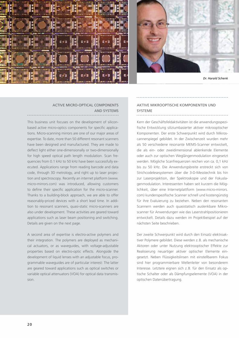
aktIVe MIkrooPtIsche koMPonenten und
systeMe
Kern der Geschäftsfeldaktivitäten ist die anwendungsspezi-
fische Entwicklung siliziumbasierter aktiver mikrooptischer
Komponenten. Der erste Schwerpunkt wird durch Mikros-
cannerspiegel gebildet. In der Zwischenzeit wurden mehr
als 50 verschiedene resonante MEMS-Scanner entwickelt,
die als ein- oder zweidimensional ablenkende Elemente
oder auch zur optischen Weglängenmodulation eingesetzt
werden. Mögliche Scanfrequenzen reichen von ca. 0,1 kHz
bis zu 50 kHz. Die Anwendungsbreite erstreckt sich von
Strichcodelesesystemen über die 3-D-Messtechnik bis hin
zur Laserprojektion, der Spektroskopie und der Fokusla-
genmodulation. Interessenten haben seit kurzem die Mög-
lichkeit, über eine Internetplattform (www.micro-mirrors.
com) kundenspezifische Scanner schnell und kostengünstig
für ihre Evaluierung zu beziehen. Neben den resonanten
Scannern werden auch quasistatisch auslenkbare Mikro-
scanner für Anwendungen wie das Laserstrahlpositionieren
entwickelt. Details dazu werden im Projektbeispiel auf der
nächsten Seite beschrieben.
Der zweite Schwerpunkt wird durch den Einsatz elektroak-
tiver Polymere gebildet. Diese werden z. B. als mechanische
Aktoren oder unter Nutzung elektrooptischer Effekte zur
Realisierung neuartiger aktiver optischer Elemente ein-
gesetzt. Neben Flüssigkeitslinsen mit einstellbarem Fokus
sind hier programmierbare Wellenleiter von besonderem
Interesse. Letztere eignen sich z. B. für den Einsatz als op-
tische Schalter oder als Dämpfungselemente (VOA) in der
optischen Datenübertragung.
actIVe MIcro-oPtIcal coMPonents
and systeMs
This business unit focuses on the development of silicon-
based active micro-optics components for specific applica-
tions. Micro-scanning mirrors are one of our major areas of
expertise. To date, more than 50 different resonant scanners
have been designed and manufactured. They are made to
deflect light either one-dimensionally or two-dimensionally
for high speed optical path length modulation. Scan fre-
quencies from 0.1 kHz to 50 kHz have been successfully ex-
ecuted. Applications range from reading barcode and data
code, through 3D metrology, and right up to laser projec-
tion and spectroscopy. Recently an internet platform (www.
micro-mirrors.com) was introduced, allowing customers
to define their specific application for the micro-scanner.
Thanks to a building-block approach, we are able to offer
reasonably-priced devices with a short lead time. In addi-
tion to resonant scanners, quasi-static micro-scanners are
also under development. These activities are geared toward
applications such as laser beam positioning and switching.
Details are given on the next page.
A second area of expertise is electro-active polymers and
their integration. The polymers are deployed as mechani-
cal actuators, or as waveguides, with voltage-adjustable
properties based on electro-optic effects. Alongside the
development of liquid lenses with an adjustable focus, pro-
grammable waveguides are of particular interest: The latter
are geared toward applications such as optical switches or
variable optical attenuators (VOA) for optical data transmis-
sion.
21
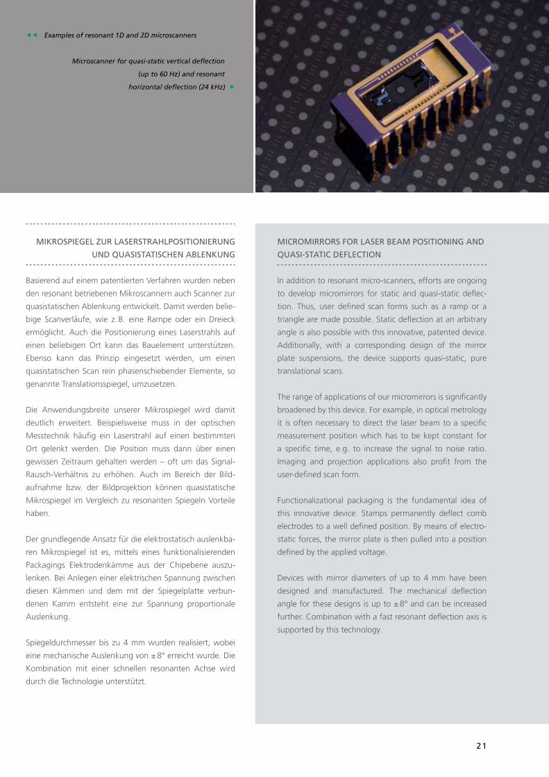
eeExamples of resonant 1D and 2D microscanners
Microscanner for quasi-static vertical deflection
(up to 60 Hz) and resonant
horizontal deflection (24 kHz)
MIcroMIrrors For laser beaM PosItIonIng and
QuasI-statIc deFlectIon
In addition to resonant micro-scanners, efforts are ongoing
to develop micromirrors for static and quasi-static deflec-
tion. Thus, user defined scan forms such as a ramp or a
triangle are made possible. Static deflection at an arbitrary
angle is also possible with this innovative, patented device.
Additionally, with a corresponding design of the mirror
plate suspensions, the device supports quasi-static, pure
translational scans.
The range of applications of our micromirrors is significantly
broadened by this device. For example, in optical metrology
it is often necessary to direct the laser beam to a specific
measurement position which has to be kept constant for
a specific time, e.g. to increase the signal to noise ratio.
Imaging and projection applications also profit from the
user-defined scan form.
Functionalizational packaging is the fundamental idea of
this innovative device. Stamps permanently deflect comb
electrodes to a well defined position. By means of electro-
static forces, the mirror plate is then pulled into a position
defined by the applied voltage.
Devices with mirror diameters of up to 4 mm have been
designed and manufactured. The mechanical deflection
angle for these designs is up to ± 8° and can be increased
further. Combination with a fast resonant deflection axis is
supported by this technology.
MIkrosPIegel zur laserstrahlPosItIonIerung
und QuasIstatIschen ablenkung
Basierend auf einem patentierten Verfahren wurden neben
den resonant betriebenen Mikroscannern auch Scanner zur
quasistatischen Ablenkung entwickelt. Damit werden belie-
bige Scanverläufe, wie z. B. eine Rampe oder ein Dreieck
ermöglicht. Auch die Positionierung eines Laserstrahls auf
einen beliebigen Ort kann das Bauelement unterstützen.
Ebenso kann das Prinzip eingesetzt werden, um einen
quasistatischen Scan rein phasenschiebender Elemente, so
genannte Translationsspiegel, umzusetzen.
Die Anwendungsbreite unserer Mikrospiegel wird damit
deutlich erweitert. Beispielsweise muss in der optischen
Messtechnik häufig ein Laserstrahl auf einen bestimmten
Ort gelenkt werden. Die Position muss dann über einen
gewissen Zeitraum gehalten werden – oft um das Signal-
Rausch-Verhältnis zu erhöhen. Auch im Bereich der Bild-
aufnahme bzw. der Bildprojektion können quasistatische
Mikrospiegel im Vergleich zu resonanten Spiegeln Vorteile
haben.
Der grundlegende Ansatz für die elektrostatisch auslenkba-
ren Mikrospiegel ist es, mittels eines funktionalisierenden
Packagings Elektrodenkämme aus der Chipebene auszu-
lenken. Bei Anlegen einer elektrischen Spannung zwischen
diesen Kämmen und dem mit der Spiegelplatte verbun-
denen Kamm entsteht eine zur Spannung proportionale
Auslenkung.
Spiegeldurchmesser bis zu 4 mm wurden realisiert, wobei
eine mechanische Auslenkung von ± 8° erreicht wurde. Die
Kombination mit einer schnellen resonanten Achse wird
durch die Technologie unterstützt.
22
FlächenlIchtModulatoren
Flächenlichtmodulatoren des Fraunhofer IPMS bestehen
aus einer Anordnung von Mikrospiegeln auf einem Halb-
leiterchip, wobei die Spiegelanzahl anwendungsspezifisch
aktuell von einigen hundert bis zu mehreren Millionen
Spiegeln variiert. Letzteres erfordert einen hochintegrierten
anwendungsspezifischen elektronischen Schaltkreis (ASIC)
als Basis der Bauelementearchitektur, um eine individuelle
analoge Einzelauslenkung jedes Mikrospiegels zu ermög-
lichen. Das Fraunhofer IPMS entwickelt darüber hinaus
Ansteuerelektronik für Spiegelarrays inklusive Software. Die
Einzelspiegel können in Abhängigkeit von der Anwendung
individuell gekippt oder abgesenkt werden, so dass ein
flächiges Muster entsteht, mit dessen Hilfe z. B. definierte
Strukturen projiziert werden.
Hochauflösende Kippspiegelarrays mit bis zu 2,3 Millionen
Einzelspiegeln werden von unseren Kunden als hochdyna-
mische programmierbare Masken für die optische Mikro-
lithographie im Ultraviolett-Bereich eingesetzt. Spiegelab-
messungen hierbei liegen bei 10 µm oder größer. Durch das
Auslenken der Mikrospiegel werden die Strukturinformati-
onen mit hoher Bildrate in den hochauflösenden Fotolack
übertragen. Weitere Anwendungsfelder liegen in der
Halbleiterinspektion und -messtechnik sowie perspektivisch
in der Laserbeschriftung, -markierung und -materialbearbei-
tung. Senkspiegelarrays, die auf 240 x 200 Einzelspiegeln
(40 x 40 μm²) basieren, finden unter anderem Anwendung
in der Wellenfrontformung in adaptiv-optischen Systemen.
Diese Systeme können z. B. Wellenfrontstörungen in weiten
Spektralbereichen korrigieren und damit die Wiedergabe-
qualität von Bildern verbessern. Darüber hinaus sind die
Bauelementefunktionalitäten besonders in der Augenheil-
kunde, Astronomie und Mikroskopie sowie bei räumlicher
und zeitlicher Laserstrahl- und Pulsformung von Interesse.
sPatIal lIght Modulators
The spatial light modulators from Fraunhofer IPMS consist
of arrays of micromirrors on semiconductor chips, whereby
the number of mirrors varies depending on the application,
from a few hundred to several millions. The latter demand
a highly integrated application specific electronic circuit
(ASIC) as the foundation for the component architecture in
order to enable an individual analogue deflection of each
micromirror. In addition, Fraunhofer IPMS develops elec-
tronics and software for mirror array control. The individual
mirrors can be tilted or vertically deflected depending on
the application, so that a surface pattern is created, for
example to project defined structures.
High resolution tilting mirror arrays with up to 2.3 million
individual mirrors are used by our customers as highly dy-
namic programmable masks for optical micro-lithography
in the ultraviolet spectral range. The mirror dimensions are
10 μm or larger. By tilting the micromirrors, structural infor-
mation is transferred to a high resolution photo resist at high
frame rates. Further fields of application are semiconductor
inspection and measurement technology, and prospectively
laser printing, marking and material processing. Piston mi-
cromirror arrays based on 240 x 200 individual mirrors
(40 x 40 μm²) can be used, among others, for wavefront
control in adaptive optical systems. These systems can, for
example, correct wavefront disturbances in broad spectrum
ranges and thereby improve image quality. The component
capabilities gain further interest, especially in the fields of
ophthalmology, astronomy and microscopy, as well as in
spatial and temporal laser beam and pulse shaping.
Dr. Michael Wagner
23
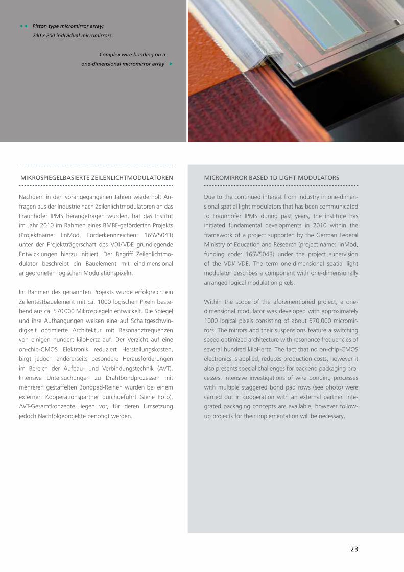
eePiston type micromirror array;
240 x 200 individual micromirrors
Complex wire bonding on a
one-dimensional micromirror array
MIkrosPIegelbasIerte zeIlenlIchtModulatoren
Nachdem in den vorangegangenen Jahren wiederholt An-
fragen aus der Industrie nach Zeilenlichtmodulatoren an das
Fraunhofer IPMS herangetragen wurden, hat das Institut
im Jahr 2010 im Rahmen eines BMBF-geförderten Projekts
(Projektname: linMod, Förderkennzeichen: 16SV5043)
unter der Projektträgerschaft des VDI / VDE grundlegende
Entwicklungen hierzu initiiert. Der Begriff Zeilenlichtmo-
dulator beschreibt ein Bauelement mit eindimensional
angeordneten logischen Modulationspixeln.
Im Rahmen des genannten Projekts wurde erfolgreich ein
Zeilentestbauelement mit ca. 1000 logischen Pixeln beste-
hend aus ca. 570 000 Mikrospiegeln entwickelt. Die Spiegel
und ihre Aufhängungen weisen eine auf Schaltgeschwin-
digkeit optimierte Architektur mit Resonanzfrequenzen
von einigen hundert kiloHertz auf. Der Verzicht auf eine
on-chip-CMOS Elektronik reduziert Herstellungskosten,
birgt jedoch andererseits besondere Herausforderungen
im Bereich der Aufbau- und Verbindungstechnik (AVT).
Intensive Untersuchungen zu Drahtbondprozessen mit
mehreren gestaffelten Bondpad-Reihen wurden bei einem
externen Kooperationspartner durchgeführt (siehe Foto).
AVT-Gesamtkonzepte liegen vor, für deren Umsetzung
jedoch Nachfolgeprojekte benötigt werden.
MIcroMIrror based 1d lIght Modulators
Due to the continued interest from industry in one-dimen-
sional spatial light modulators that has been communicated
to Fraunhofer IPMS during past years, the institute has
initiated fundamental developments in 2010 within the
framework of a project supported by the German Federal
Ministry of Education and Research (project name: linMod,
funding code: 16SV5043) under the project supervision
of the VDI/ VDE. The term one-dimensional spatial light
modulator describes a component with one-dimensionally
arranged logical modulation pixels.
Within the scope of the aforementioned project, a one-
dimensional modulator was developed with approximately
1000 logical pixels consisting of about 570,000 micromir-
rors. The mirrors and their suspensions feature a switching
speed optimized architecture with resonance frequencies of
several hundred kiloHertz. The fact that no on-chip-CMOS
electronics is applied, reduces production costs, however it
also presents special challenges for backend packaging pro-
cesses. Intensive investigations of wire bonding processes
with multiple staggered bond pad rows (see photo) were
carried out in cooperation with an external partner. Inte-
grated packaging concepts are available, however follow-
up projects for their implementation will be necessary.
24
sensor and actuator systeMs
The business unit “Sensor & Actuator Systems” develops
complete components and devices, right up to demon-
strators and prototypes, typically resulting in miniaturized
solutions. These systems combine sensors and actuators
developed by Fraunhofer IPMS with ASICs designed at
Fraunhofer IPMS, discrete electronics, and also include
hardware development services, software and optics system
design.
The work is currently focused on three fields of application:
The work on personalized information systems includes all
aspects of image and video presentation on mobile devices.
It ranges from ultra-compact laser projection systems which
utilize Fraunhofer IPMS’ micro-scanning mirror for innova-
tive architecture of auto-stereoscopic 3D displays, which
enables simultaneous viewing by several people without
any limitations in the geometrical resolution of the image.
Imaging systems make especial use of Fraunhofer IMPS’
own micro-scanning mirror for systems capable of 2D and
3D acquisition of image information for applications in
endoscopy, laser range finders and surveillance.
Finally, optics systems development incorporates spectros-
copy on the one hand with highly compact spectrometers
and systems for hyper-spectral imaging and fully-reflective
optical systems on the other hand. This makes applications
covering an extremely broad wavelength possible.
sensor- und aktorsysteMe
Das Geschäftsfeld »Sensor & Actuator Systems« ent-
wickelt vollständige Komponenten und Geräte bis hin
zum Demonstrator und Prototypen. Durch Kombination
der am Institut entwickelten Sensoren und Aktoren mit
Ansteuerschaltkreisen (ASICs), diskreter Elektronik, Optik
und Software ergeben sich Systeme mit möglichst geringer
Baugröße.
Das Geschäftsfeld konzentriert sich auf drei Schwerpunkt-
themen: Personalisierte Informationssysteme umfassen alle
Entwicklungen, die der Darstellung von bildlicher Informa-
tion in Kombination mit portablen Endgeräten dienen. Dies
reicht von ultrakompakten Laserprojektionssystemen unter
Nutzung der Mikroscannerspiegel des Fraunhofer IPMS
bis zu neuartigen autostereoskopischen 3-D-Displays, bei
denen gleichzeitig mehrere Betrachter einen dreidimensi-
onalen Eindruck der präsentierten Szene erhalten – ohne
Einschränkungen hinsichtlich der geometrischen Auflösung
des Bildes.
Systeme zur Bilderfassung nutzen insbesondere die am
Fraunhofer IPMS entwickelten Mikroscannerspiegel für
Lösungen zur zwei- und dreidimensionalen Erfassung von
Bildinformation. Anwendungsfelder liegen z. B. in der Endo-
skopie, der Laser-gestützten Entfernungsmessung und der
optischen Überwachung von Räumen.
Der dritte Bereich der Optischen Systeme umfasst zum ei-
nen die Spektroskopie mit sehr kompakten Spektrometern
als auch Systemen für Hyperspectral Imaging und zum
anderen voll-reflektive Optiken, die in einem sehr weiten
Wellenlängenbereich eingesetzt werden können.
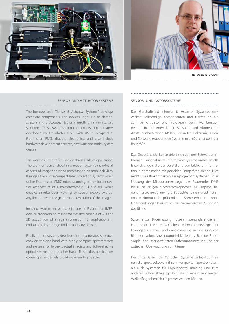
Dr. Michael Scholles
25
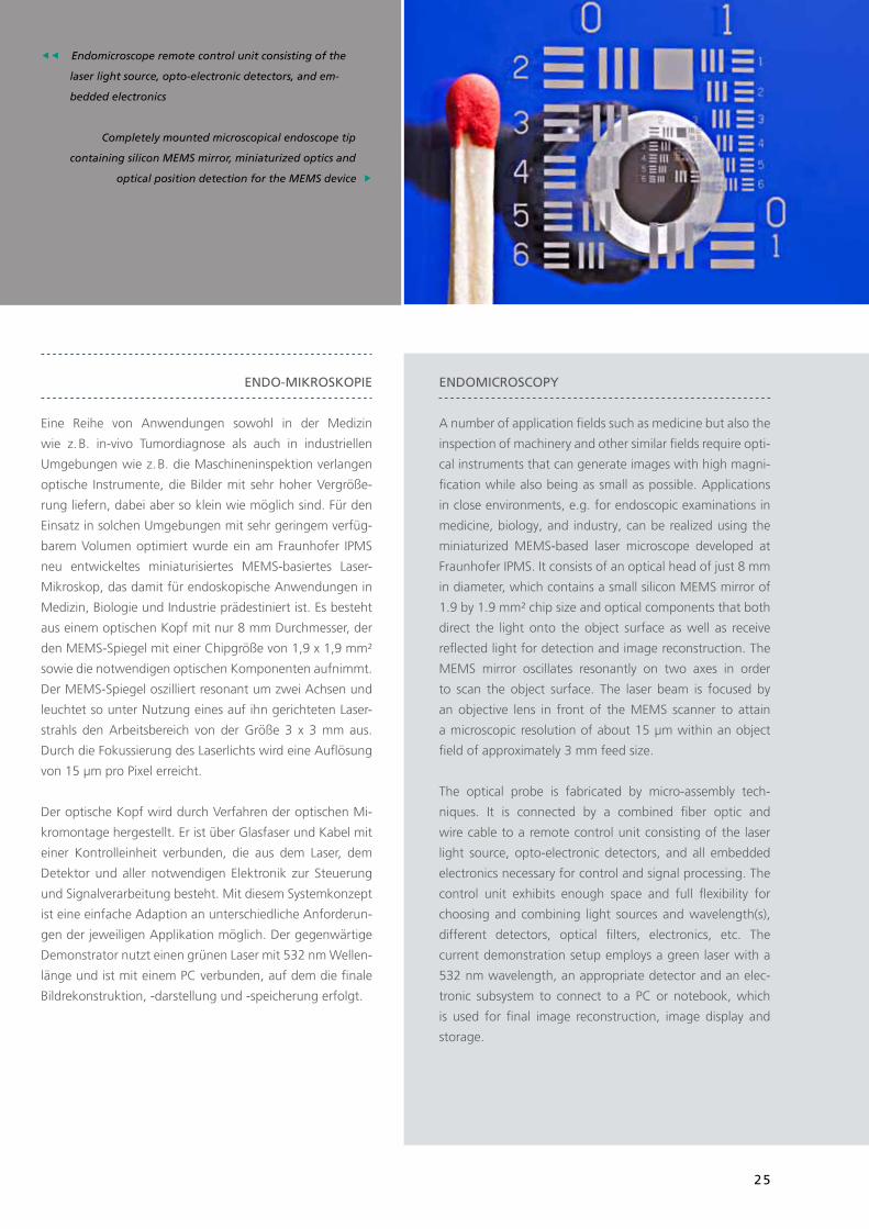
eeEndomicroscope remote control unit consisting of the
laser light source, opto-electronic detectors, and em-
bedded electronics
Completely mounted microscopical endoscope tip
containing silicon MEMS mirror, miniaturized optics and
optical position detection for the MEMS device
endoMIcroscoPy
A number of application fields such as medicine but also the
inspection of machinery and other similar fields require opti-
cal instruments that can generate images with high magni-
fication while also being as small as possible. Applications
in close environments, e.g. for endoscopic examinations in
medicine, biology, and industry, can be realized using the
miniaturized MEMS-based laser microscope developed at
Fraunhofer IPMS. It consists of an optical head of just 8 mm
in diameter, which contains a small silicon MEMS mirror of
1.9 by 1.9 mm² chip size and optical components that both
direct the light onto the object surface as well as receive
reflected light for detection and image reconstruction. The
MEMS mirror oscillates resonantly on two axes in order
to scan the object surface. The laser beam is focused by
an objective lens in front of the MEMS scanner to attain
a microscopic resolution of about 15 µm within an object
field of approximately 3 mm feed size.
The optical probe is fabricated by micro-assembly tech-
niques. It is connected by a combined fiber optic and
wire cable to a remote control unit consisting of the laser
light source, opto-electronic detectors, and all embedded
electronics necessary for control and signal processing. The
control unit exhibits enough space and full flexibility for
choosing and combining light sources and wavelength(s),
different detectors, optical filters, electronics, etc. The
current demonstration setup employs a green laser with a
532 nm wavelength, an appropriate detector and an elec-
tronic subsystem to connect to a PC or notebook, which
is used for final image reconstruction, image display and
storage.
endo-MIkroskoPIe
Eine Reihe von Anwendungen sowohl in der Medizin
wie z. B. in-vivo Tumordiagnose als auch in industriellen
Umgebungen wie z. B. die Maschineninspektion verlangen
optische Instrumente, die Bilder mit sehr hoher Vergröße-
rung liefern, dabei aber so klein wie möglich sind. Für den
Einsatz in solchen Umgebungen mit sehr geringem verfüg-
barem Volumen optimiert wurde ein am Fraunhofer IPMS
neu entwickeltes miniaturisiertes MEMS-basiertes Laser-
Mikroskop, das damit für endoskopische Anwendungen in
Medizin, Biologie und Industrie prädestiniert ist. Es besteht
aus einem optischen Kopf mit nur 8 mm Durchmesser, der
den MEMS-Spiegel mit einer Chipgröße von 1,9 x 1,9 mm²
sowie die notwendigen optischen Komponenten aufnimmt.
Der MEMS-Spiegel oszilliert resonant um zwei Achsen und
leuchtet so unter Nutzung eines auf ihn gerichteten Laser-
strahls den Arbeitsbereich von der Größe 3 x 3 mm aus.
Durch die Fokussierung des Laserlichts wird eine Auflösung
von 15 µm pro Pixel erreicht.
Der optische Kopf wird durch Verfahren der optischen Mi-
kromontage hergestellt. Er ist über Glasfaser und Kabel mit
einer Kontrolleinheit verbunden, die aus dem Laser, dem
Detektor und aller notwendigen Elektronik zur Steuerung
und Signalverarbeitung besteht. Mit diesem Systemkonzept
ist eine einfache Adaption an unterschiedliche Anforderun-
gen der jeweiligen Applikation möglich. Der gegenwärtige
Demonstrator nutzt einen grünen Laser mit 532 nm Wellen-
länge und ist mit einem PC verbunden, auf dem die finale
Bildrekonstruktion, -darstellung und -speicherung erfolgt.
26
drahtlose MIkrosysteMe
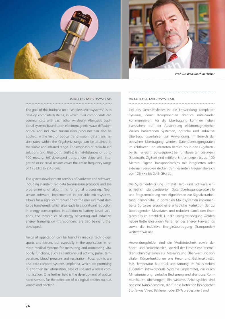
Ziel des Geschäftsfeldes ist die Entwicklung kompletter
Systeme, deren Komponenten drahtlos miteinander
kommunizieren. Für die Übertragung kommen neben
klassischen, auf der Ausbreitung elektromagnetischer
Wellen basierenden Systemen, optische und induktive
Übertragungsverfahren zur Anwendung. Im Bereich der
optischen Übertragung werden Datenübertragungsraten
im sichtbaren und infraroten Bereich bis in den Gigahertz-
bereich erreicht. Schwerpunkt bei funkbasierten Lösungen
(Bluetooth, ZigBee) sind mittlere Entfernungen bis zu 100
Metern. Eigene Transponderchips mit integrierten oder
externen Sensoren decken den gesamten Frequenzbereich
von 125 kHz bis 2,45 GHz ab.
Die Systementwicklung umfasst Hard- und Software ein-
schließlich standardisierter Datenübertragungsprotokolle
und Programmierung von Algorithmen zur Signalverarbei-
tung. Sensornahe, in portablen Mikrosystemen implemen-
tierte Software erlaubt eine erhebliche Reduktion der zu
übertragenden Messdaten und reduziert damit den Ener-
gieverbrauch erheblich. Für die Energieversorgung werden
neben Batterielösungen Verfahren des Energy Harvestings
sowie die induktive Energieübertragung (Transponder)
weiterentwickelt.
Anwendungsfelder sind die Medizintechnik sowie der
Sport- und Freizeitbereich, speziell der Einsatz von teleme-
dizinischen Systemen zur Messung und Überwachung von
vitalen Körperfunktionen wie Herz- und Gehirnaktivität,
Puls, Temperatur, Blutdruck und Atmung. Im Fokus stehen
außerdem intrakorporale Systeme (Implantate), die durch
Miniaturisierung, einfache Bedienung und drahtlose Kom-
munikation überzeugen. Ein weiteres Arbeitsgebiet sind
optische Nano-Sensoren, die für die Detektion biologischer
Stoffe wie Viren, Bakterien oder DNA prädestiniert sind.
wIreless MIcrosysteMs
The goal of this business unit “Wireless Microsystems” is to
develop complete systems, in which their components can
communicate with each other wirelessly. Alongside tradi-
tional systems based upon electromagnetic wave diffusion,
optical and inductive transmission processes can also be
applied. In the field of optical transmission, data transmis-
sion rates within the Gigahertz range can be attained in
the visible and infrared range. The emphasis of radio-based
solutions (e.g. Bluetooth, ZigBee) is mid-distances of up to
100 meters. Self-developed transponder chips with inte-
grated or external sensors cover the entire frequency range
of 125 kHz to 2.45 GHz.
The system development consists of hardware and software,
including standardized data transmission protocols and the
programming of algorithms for signal processing. Near-
sensor software, implemented in portable microsystems,
allows for a significant reduction of the measurement data
to be transferred, which also leads to a significant reduction
in energy consumption. In addition to battery-based solu-
tions, the techniques of energy harvesting and inductive
energy transmission (transponders) are also being further
developed.
Fields of application can be found in medical technology,
sports and leisure, but especially in the application in re-
mote medical systems for measuring and monitoring vital
bodily functions, such as cardio-neural activity, pulse, tem-
perature, blood pressure and respiration. Focal points are
also intra-corporal systems (implants), which are promising
due to their miniaturization, ease of use and wireless com-
munication. One further field is the development of optical
nano-sensors for the detection of biological entities such as
viruses and bacteria.
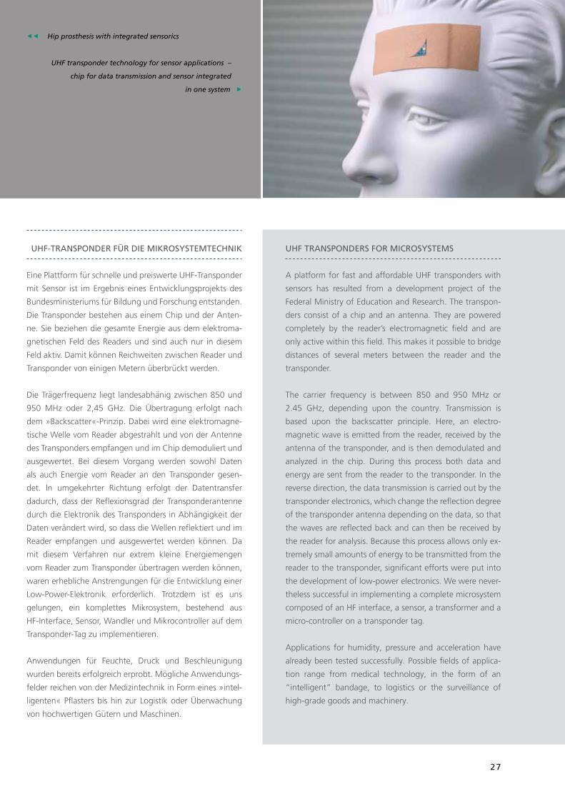
Prof. Dr. Wolf-Joachim Fischer
27
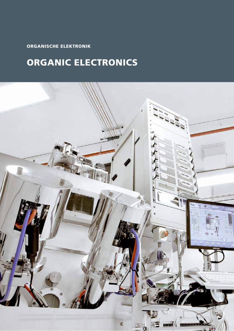
uhF transPonders For MIcrosysteMs
A platform for fast and affordable UHF transponders with
sensors has resulted from a development project of the
Federal Ministry of Education and Research. The transpon-
ders consist of a chip and an antenna. They are powered
completely by the reader’s electromagnetic field and are
only active within this field. This makes it possible to bridge
distances of several meters between the reader and the
transponder.
The carrier frequency is between 850 and 950 MHz or
2.45 GHz, depending upon the country. Transmission is
based upon the backscatter principle. Here, an electro-
magnetic wave is emitted from the reader, received by the
antenna of the transponder, and is then demodulated and
analyzed in the chip. During this process both data and
energy are sent from the reader to the transponder. In the
reverse direction, the data transmission is carried out by the
transponder electronics, which change the reflection degree
of the transponder antenna depending on the data, so that
the waves are reflected back and can then be received by
the reader for analysis. Because this process allows only ex-
tremely small amounts of energy to be transmitted from the
reader to the transponder, significant efforts were put into
the development of low-power electronics. We were never-
theless successful in implementing a complete microsystem
composed of an HF interface, a sensor, a transformer and a
micro-controller on a transponder tag.
Applications for humidity, pressure and acceleration have
already been tested successfully. Possible fields of applica-
tion range from medical technology, in the form of an
“intelligent” bandage, to logistics or the surveillance of
high-grade goods and machinery.
ee Hip prosthesis with integrated sensorics
UHF transponder technology for sensor applications –
chip for data transmission and sensor integrated
in one system
uhF-transPonder Für dIe MIkrosysteMtechnIk
Eine Plattform für schnelle und preiswerte UHF-Transponder
mit Sensor ist im Ergebnis eines Entwicklungsprojekts des
Bundesministeriums für Bildung und Forschung entstanden.
Die Transponder bestehen aus einem Chip und der Anten-
ne. Sie beziehen die gesamte Energie aus dem elektroma-
gnetischen Feld des Readers und sind auch nur in diesem
Feld aktiv. Damit können Reichweiten zwischen Reader und
Transponder von einigen Metern überbrückt werden.
Die Trägerfrequenz liegt landesabhänig zwischen 850 und
950 MHz oder 2,45 GHz. Die Übertragung erfolgt nach
dem »Backscatter«-Prinzip. Dabei wird eine elektromagne-
tische Welle vom Reader abgestrahlt und von der Antenne
des Transponders empfangen und im Chip demoduliert und
ausgewertet. Bei diesem Vorgang werden sowohl Daten
als auch Energie vom Reader an den Transponder gesen-
det. In umgekehrter Richtung erfolgt der Datentransfer
dadurch, dass der Reflexionsgrad der Transponderantenne
durch die Elektronik des Transponders in Abhängigkeit der
Daten verändert wird, so dass die Wellen reflektiert und im
Reader empfangen und ausgewertet werden können. Da
mit diesem Verfahren nur extrem kleine Energiemengen
vom Reader zum Transponder übertragen werden können,
waren erhebliche Anstrengungen für die Entwicklung einer
Low-Power-Elektronik erforderlich. Trotzdem ist es uns
gelungen, ein komplettes Mikrosystem, bestehend aus
HF-Interface, Sensor, Wandler und Mikrocontroller auf dem
Transponder-Tag zu implementieren.
Anwendungen für Feuchte, Druck und Beschleunigung
wurden bereits erfolgreich erprobt. Mögliche Anwendungs-
felder reichen von der Medizintechnik in Form eines »intel-
ligenten« Pflasters bis hin zur Logistik oder Überwachung
von hochwertigen Gütern und Maschinen.
28
organIsche elektronIk
organIc electronIcs
29
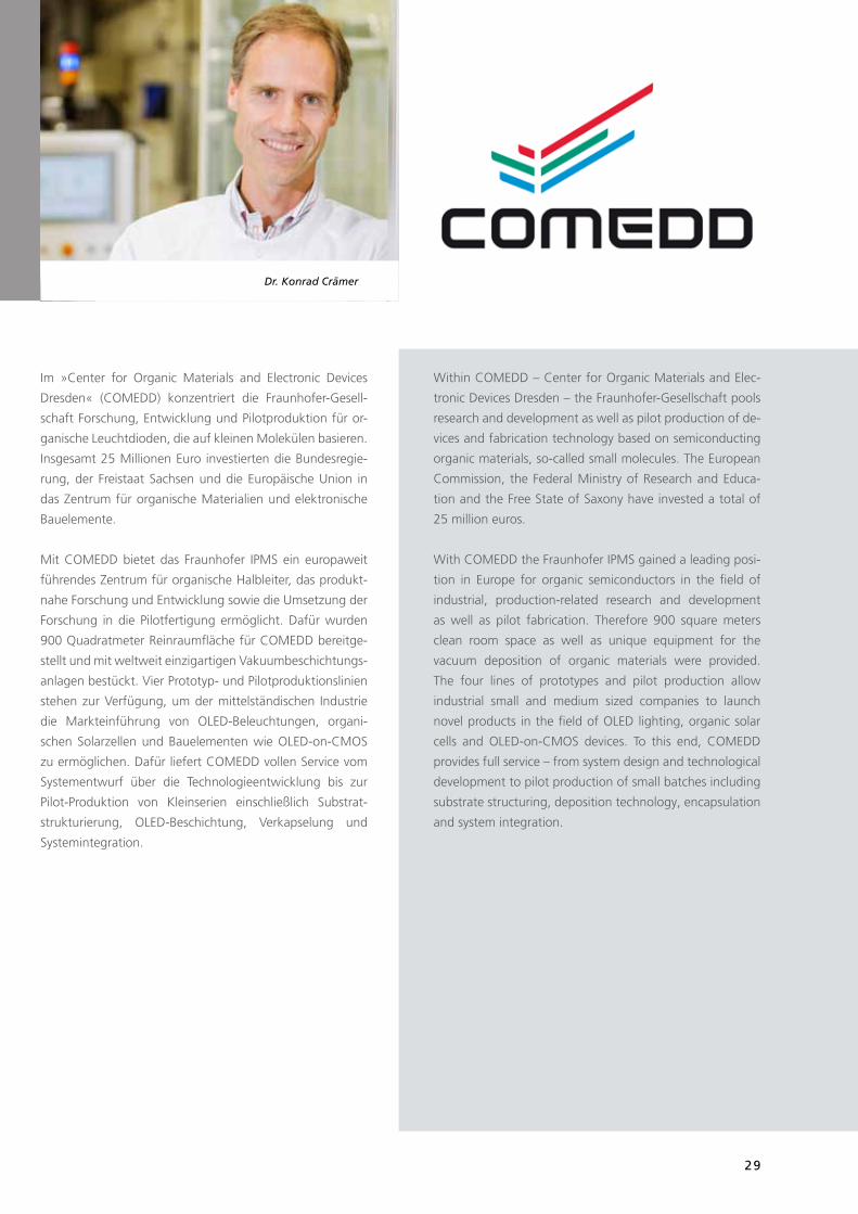
Within COMEDD – Center for Organic Materials and Elec-
tronic Devices Dresden – the Fraunhofer-Gesellschaft pools
research and development as well as pilot production of de-
vices and fabrication technology based on semiconducting
organic materials, so-called small molecules. The European
Commission, the Federal Ministry of Research and Educa-
tion and the Free State of Saxony have invested a total of
25 million euros.
With COMEDD the Fraunhofer IPMS gained a leading posi-
tion in Europe for organic semiconductors in the field of
industrial, production-related research and development
as well as pilot fabrication. Therefore 900 square meters
clean room space as well as unique equipment for the
vacuum deposition of organic materials were provided.
The four lines of prototypes and pilot production allow
industrial small and medium sized companies to launch
novel products in the field of OLED lighting, organic solar
cells and OLED-on-CMOS devices. To this end, COMEDD
provides full service – from system design and technological
development to pilot production of small batches including
substrate structuring, deposition technology, encapsulation
and system integration.
Im »Center for Organic Materials and Electronic Devices
Dresden« (COMEDD) konzentriert die Fraunhofer-Gesell-
schaft Forschung, Entwicklung und Pilotproduktion für or-
ganische Leuchtdioden, die auf kleinen Molekülen basieren.
Insgesamt 25 Millionen Euro investierten die Bundesregie-
rung, der Freistaat Sachsen und die Europäische Union in
das Zentrum für organische Materialien und elektronische
Bauelemente.
Mit COMEDD bietet das Fraunhofer IPMS ein europaweit
führendes Zentrum für organische Halbleiter, das produkt-
nahe Forschung und Entwicklung sowie die Umsetzung der
Forschung in die Pilotfertigung ermöglicht. Dafür wurden
900 Quadratmeter Reinraumfläche für COMEDD bereitge-
stellt und mit weltweit einzigartigen Vakuumbeschichtungs-
anlagen bestückt. Vier Prototyp- und Pilotproduktionslinien
stehen zur Verfügung, um der mittelständischen Industrie
die Markteinführung von OLED-Beleuchtungen, organi-
schen Solarzellen und Bauelementen wie OLED-on-CMOS
zu ermöglichen. Dafür liefert COMEDD vollen Service vom
Systementwurf über die Technologieentwicklung bis zur
Pilot-Produktion von Kleinserien einschließlich Substrat-
strukturierung, OLED-Beschichtung, Verkapselung und
Systemintegration.
Dr. Konrad Crämer
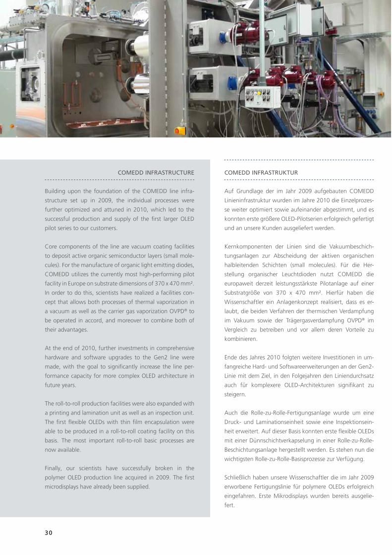
30
Dr. Harald Schenk
coMedd InFrastruktur
Auf Grundlage der im Jahr 2009 aufgebauten COMEDD
Linieninfrastruktur wurden im Jahre 2010 die Einzelprozes-
se weiter optimiert sowie aufeinander abgestimmt, und es
konnten erste größere OLED-Pilotserien erfolgreich gefertigt
und an unsere Kunden ausgeliefert werden.
Kernkomponenten der Linien sind die Vakuumbeschich-
tungsanlagen zur Abscheidung der aktiven organischen
halbleitenden Schichten (small molecules). Für die Her-
stellung organischer Leuchtdioden nutzt COMEDD die
europaweit derzeit leistungsstärkste Pilotanlage auf einer
Substratgröße von 370 x 470 mm². Hierfür haben die
Wissenschaftler ein Anlagenkonzept realisiert, dass es er-
laubt, die beiden Verfahren der thermischen Verdampfung
im Vakuum sowie der Trägergasverdampfung OVPD® im
Vergleich zu betreiben und vor allem deren Vorteile zu
kombinieren.
Ende des Jahres 2010 folgten weitere Investitionen in um-
fangreiche Hard- und Softwareerweiterungen an der Gen2-
Linie mit dem Ziel, in den Folgejahren den Liniendurchsatz
auch für komplexere OLED-Architekturen signifikant zu
steigern.
Auch die Rolle-zu-Rolle-Fertigungsanlage wurde um eine
Druck- und Laminationseinheit sowie eine Inspektionsein-
heit erweitert. Auf dieser Basis konnten erste flexible OLEDs
mit einer Dünnschichtverkapselung in einer Rolle-zu-Rolle-
Beschichtungsanlage hergestellt werden. Es stehen nun die
wichtigsten Rolle-zu-Rolle-Basisprozesse zur Verfügung.
Schließlich haben unsere Wissenschaftler die im Jahr 2009
erworbene Fertigungslinie für polymere OLEDs erfolgreich
eingefahren. Erste Mikrodisplays wurden bereits ausgelie-
fert.
coMedd InFrastructure
Building upon the foundation of the COMEDD line infra-
structure set up in 2009, the individual processes were
further optimized and attuned in 2010, which led to the
successful production and supply of the first larger OLED
pilot series to our customers.
Core components of the line are vacuum coating facilities
to deposit active organic semiconductor layers (small mole-
cules). For the manufacture of organic light emitting diodes,
COMEDD utilizes the currently most high-performing pilot
facility in Europe on substrate dimensions of 370 x 470 mm².
In order to do this, scientists have realized a facilities con-
cept that allows both processes of thermal vaporization in
a vacuum as well as the carrier gas vaporization OVPD® to
be operated in accord, and moreover to combine both of
their advantages.
At the end of 2010, further investments in comprehensive
hardware and software upgrades to the Gen2 line were
made, with the goal to significantly increase the line per-
formance capacity for more complex OLED architecture in
future years.
The roll-to-roll production facilities were also expanded with
a printing and lamination unit as well as an inspection unit.
The first flexible OLEDs with thin film encapsulation were
able to be produced in a roll-to-roll coating facility on this
basis. The most important roll-to-roll basic processes are
now available.
Finally, our scientists have successfully broken in the
polymer OLED production line acquired in 2009. The first
microdisplays have already been supplied.
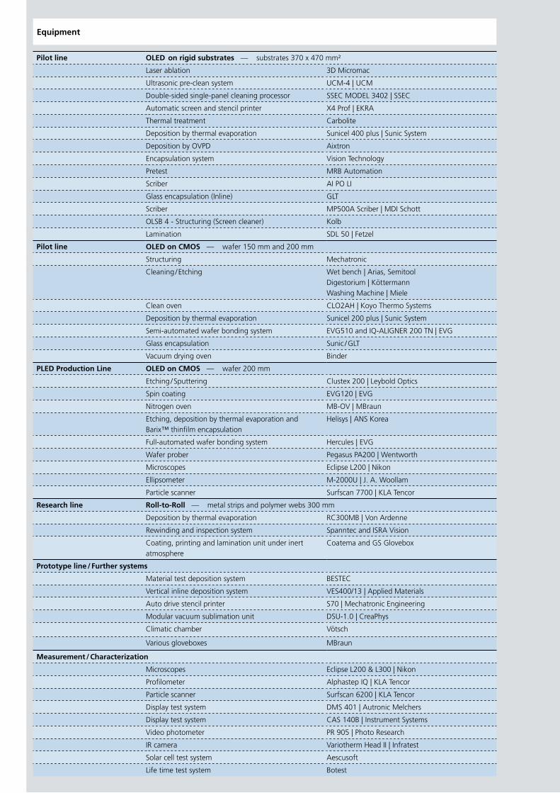
31
überschrIFt
Text
Pilot line OLED on rigid substrates — substrates 370 x 470 mm²
Laser ablation 3D Micromac
Ultrasonic pre-clean system UCM-4 | UCM
Double-sided single-panel cleaning processor SSEC MODEL 3402 | SSEC
Automatic screen and stencil printer X4 Prof | EKRA
Thermal treatment Carbolite
Deposition by thermal evaporation Sunicel 400 plus | Sunic System
Deposition by OVPD Aixtron
Encapsulation system Vision Technology
Pretest MRB Automation
Scriber AI PO LI
Glass encapsulation (Inline) GLT
Scriber MP500A Scriber | MDI Schott
OLSB 4 - Structuring (Screen cleaner) Kolb
Lamination SDL 50 | Fetzel
Pilot line OLED on CMOS — wafer 150 mm and 200 mm
Structuring Mechatronic
Cleaning / Etching Wet bench | Arias, Semitool Digestorium | Köttermann Washing Machine | Miele
Clean oven CLO2AH | Koyo Thermo Systems
Deposition by thermal evaporation Sunicel 200 plus | Sunic System
Semi-automated wafer bonding system EVG510 and IQ-ALIGNER 200 TN | EVG
Glass encapsulation Sunic / GLT
Vacuum drying oven Binder
PLED Production Line OLED on CMOS — wafer 200 mm
Etching / Sputtering Clustex 200 | Leybold Optics
Spin coating EVG120 | EVG
Nitrogen oven MB-OV | MBraun
Etching, deposition by thermal evaporation and Barix™ thinfilm encapsulation
Helisys | ANS Korea
Full-automated wafer bonding system Hercules | EVG
Wafer prober Pegasus PA200 | Wentworth
Microscopes Eclipse L200 | Nikon
Ellipsometer M-2000U | J. A. Woollam
Particle scanner Surfscan 7700 | KLA Tencor
Research line Roll-to-Roll — metal strips and polymer webs 300 mm
Deposition by thermal evaporation RC300MB | Von Ardenne
Rewinding and inspection system Spanntec and ISRA Vision
Coating, printing and lamination unit under inert atmosphere
Coatema and GS Glovebox
Prototype line / Further systems
Material test deposition system BESTEC
Vertical inline deposition system VES400/13 | Applied Materials
Auto drive stencil printer S70 | Mechatronic Engineering
Modular vacuum sublimation unit DSU-1.0 | CreaPhys
Climatic chamber Vötsch
Various gloveboxes MBraun
Measurement / Characterization
Microscopes Eclipse L200 & L300 | Nikon
Profilometer Alphastep IQ | KLA Tencor
Particle scanner Surfscan 6200 | KLA Tencor
Display test system DMS 401 | Autronic Melchers
Display test system CAS 140B | Instrument Systems
Video photometer PR 905 | Photo Research
IR camera Variotherm Head II | Infratest
Solar cell test system Aescusoft
Life time test system Botest
Equipment
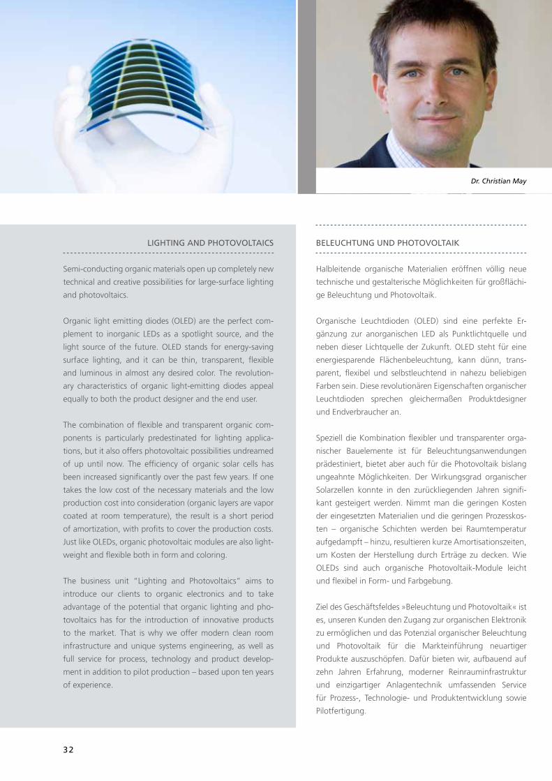
32
beleuchtung und PhotoVoltaIk
Halbleitende organische Materialien eröffnen völlig neue
technische und gestalterische Möglichkeiten für großflächi-
ge Beleuchtung und Photovoltaik.
Organische Leuchtdioden (OLED) sind eine perfekte Er-
gänzung zur anorganischen LED als Punktlichtquelle und
neben dieser Lichtquelle der Zukunft. OLED steht für eine
energiesparende Flächenbeleuchtung, kann dünn, trans-
parent, flexibel und selbstleuchtend in nahezu beliebigen
Farben sein. Diese revolutionären Eigenschaften organischer
Leuchtdioden sprechen gleichermaßen Produktdesigner
und Endverbraucher an.
Speziell die Kombination flexibler und transparenter orga-
nischer Bauelemente ist für Beleuchtungsanwendungen
prädestiniert, bietet aber auch für die Photovoltaik bislang
ungeahnte Möglichkeiten. Der Wirkungsgrad organischer
Solarzellen konnte in den zurückliegenden Jahren signifi-
kant gesteigert werden. Nimmt man die geringen Kosten
der eingesetzten Materialien und die geringen Prozesskos-
ten – organische Schichten werden bei Raumtemperatur
aufgedampft – hinzu, resultieren kurze Amortisationszeiten,
um Kosten der Herstellung durch Erträge zu decken. Wie
OLEDs sind auch organische Photovoltaik-Module leicht
und flexibel in Form- und Farbgebung.
Ziel des Geschäftsfeldes »Beleuchtung und Photovoltaik« ist
es, unseren Kunden den Zugang zur organischen Elektronik
zu ermöglichen und das Potenzial organischer Beleuchtung
und Photovoltaik für die Markteinführung neuartiger
Produkte auszuschöpfen. Dafür bieten wir, aufbauend auf
zehn Jahren Erfahrung, moderner Reinrauminfrastruktur
und einzigartiger Anlagentechnik umfassenden Service
für Prozess-, Technologie- und Produktentwicklung sowie
Pilotfertigung.
lIghtIng and PhotoVoltaIcs
Semi-conducting organic materials open up completely new
technical and creative possibilities for large-surface lighting
and photovoltaics.
Organic light emitting diodes (OLED) are the perfect com-
plement to inorganic LEDs as a spotlight source, and the
light source of the future. OLED stands for energy-saving
surface lighting, and it can be thin, transparent, flexible
and luminous in almost any desired color. The revolution-
ary characteristics of organic light-emitting diodes appeal
equally to both the product designer and the end user.
The combination of flexible and transparent organic com-
ponents is particularly predestinated for lighting applica-
tions, but it also offers photovoltaic possibilities undreamed
of up until now. The efficiency of organic solar cells has
been increased significantly over the past few years. If one
takes the low cost of the necessary materials and the low
production cost into consideration (organic layers are vapor
coated at room temperature), the result is a short period
of amortization, with profits to cover the production costs.
Just like OLEDs, organic photovoltaic modules are also light-
weight and flexible both in form and coloring.
The business unit “Lighting and Photovoltaics” aims to
introduce our clients to organic electronics and to take
advantage of the potential that organic lighting and pho-
tovoltaics has for the introduction of innovative products
to the market. That is why we offer modern clean room
infrastructure and unique systems engineering, as well as
full service for process, technology and product develop-
ment in addition to pilot production – based upon ten years
of experience.
Dr. Christian May
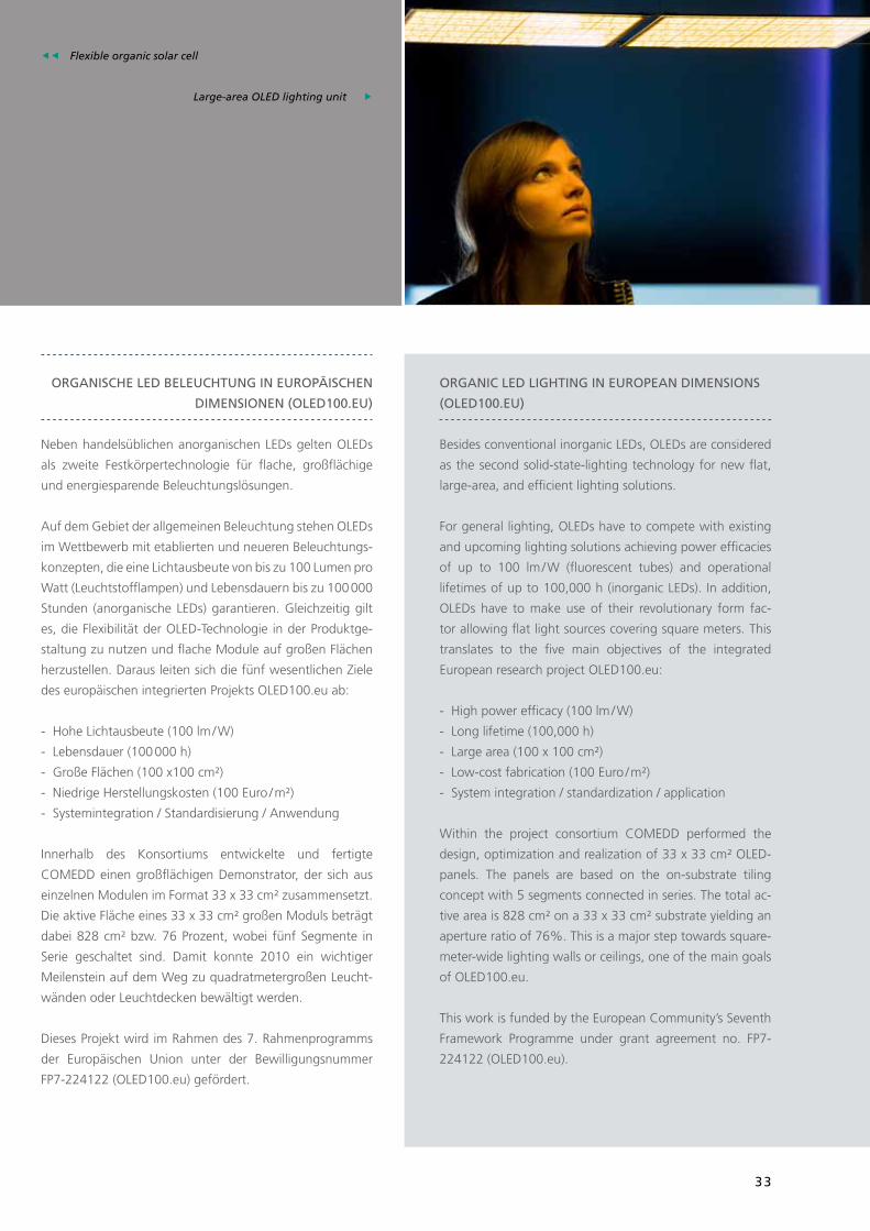
33
organIc led lIghtIng In euroPean dIMensIons
(oled100.eu)
Besides conventional inorganic LEDs, OLEDs are considered
as the second solid-state-lighting technology for new flat,
large-area, and efficient lighting solutions.
For general lighting, OLEDs have to compete with existing
and upcoming lighting solutions achieving power efficacies
of up to 100 lm / W (fluorescent tubes) and operational
lifetimes of up to 100,000 h (inorganic LEDs). In addition,
OLEDs have to make use of their revolutionary form fac-
tor allowing flat light sources covering square meters. This
translates to the five main objectives of the integrated
European research project OLED100.eu:
- High power efficacy (100 lm / W)
- Long lifetime (100,000 h)
- Large area (100 x 100 cm²)
- Low-cost fabrication (100 Euro / m²)
- System integration / standardization / application
Within the project consortium COMEDD performed the
design, optimization and realization of 33 x 33 cm² OLED-
panels. The panels are based on the on-substrate tiling
concept with 5 segments connected in series. The total ac-
tive area is 828 cm² on a 33 x 33 cm² substrate yielding an
aperture ratio of 76%. This is a major step towards square-
meter-wide lighting walls or ceilings, one of the main goals
of OLED100.eu.
This work is funded by the European Community’s Seventh
Framework Programme under grant agreement no. FP7-
224122 (OLED100.eu).
organIsche led beleuchtung In euroPäIschen
dIMensIonen (oled100.eu)
Neben handelsüblichen anorganischen LEDs gelten OLEDs
als zweite Festkörpertechnologie für flache, großflächige
und energiesparende Beleuchtungslösungen.
Auf dem Gebiet der allgemeinen Beleuchtung stehen OLEDs
im Wettbewerb mit etablierten und neueren Beleuchtungs-
konzepten, die eine Lichtausbeute von bis zu 100 Lumen pro
Watt (Leuchtstofflampen) und Lebensdauern bis zu 100 000
Stunden (anorganische LEDs) garantieren. Gleichzeitig gilt
es, die Flexibilität der OLED-Technologie in der Produktge-
staltung zu nutzen und flache Module auf großen Flächen
herzustellen. Daraus leiten sich die fünf wesentlichen Ziele
des europäischen integrierten Projekts OLED100.eu ab:
- Hohe Lichtausbeute (100 lm / W)
- Lebensdauer (100 000 h)
- Große Flächen (100 x100 cm²)
- Niedrige Herstellungskosten (100 Euro / m²)
- Systemintegration / Standardisierung / Anwendung
Innerhalb des Konsortiums entwickelte und fertigte
COMEDD einen großflächigen Demonstrator, der sich aus
einzelnen Modulen im Format 33 x 33 cm² zusammensetzt.
Die aktive Fläche eines 33 x 33 cm² großen Moduls beträgt
dabei 828 cm² bzw. 76 Prozent, wobei fünf Segmente in
Serie geschaltet sind. Damit konnte 2010 ein wichtiger
Meilenstein auf dem Weg zu quadratmetergroßen Leucht-
wänden oder Leuchtdecken bewältigt werden.
Dieses Projekt wird im Rahmen des 7. Rahmenprogramms
der Europäischen Union unter der Bewilligungsnummer
FP7-224122 (OLED100.eu) gefördert.
eeFlexible organic solar cell
Large-area OLED lighting unit
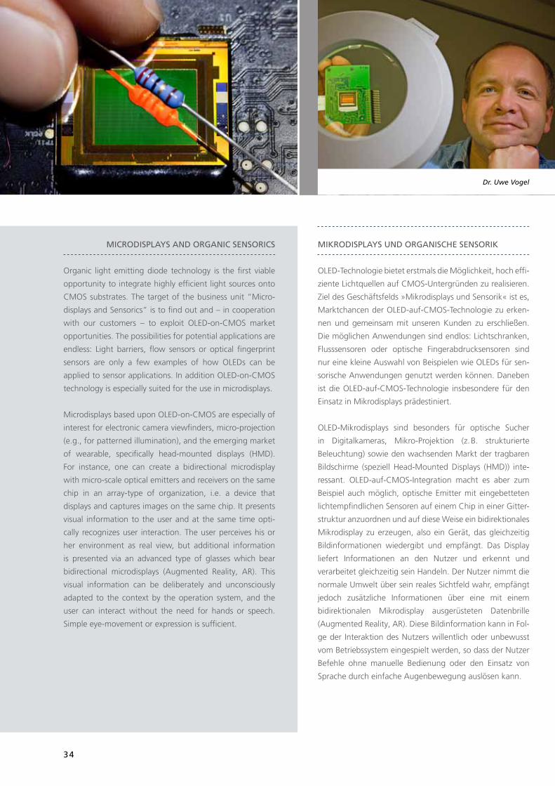
34
MIkrodIsPlays und organIsche sensorIk
OLED-Technologie bietet erstmals die Möglichkeit, hoch effi-
ziente Lichtquellen auf CMOS-Untergründen zu realisieren.
Ziel des Geschäftsfelds »Mikrodisplays und Sensorik« ist es,
Marktchancen der OLED-auf-CMOS-Technologie zu erken-
nen und gemeinsam mit unseren Kunden zu erschließen.
Die möglichen Anwendungen sind endlos: Lichtschranken,
Flusssensoren oder optische Fingerabdrucksensoren sind
nur eine kleine Auswahl von Beispielen wie OLEDs für sen-
sorische Anwendungen genutzt werden können. Daneben
ist die OLED-auf-CMOS-Technologie insbesondere für den
Einsatz in Mikrodisplays prädestiniert.
OLED-Mikrodisplays sind besonders für optische Sucher
in Digitalkameras, Mikro-Projektion (z. B. strukturierte
Beleuchtung) sowie den wachsenden Markt der tragbaren
Bildschirme (speziell Head-Mounted Displays (HMD)) inte-
ressant. OLED-auf-CMOS-Integration macht es aber zum
Beispiel auch möglich, optische Emitter mit eingebetteten
lichtempfindlichen Sensoren auf einem Chip in einer Gitter-
struktur anzuordnen und auf diese Weise ein bidirektionales
Mikrodisplay zu erzeugen, also ein Gerät, das gleichzeitig
Bildinformationen wiedergibt und empfängt. Das Display
liefert Informationen an den Nutzer und erkennt und
verarbeitet gleichzeitig sein Handeln. Der Nutzer nimmt die
normale Umwelt über sein reales Sichtfeld wahr, empfängt
jedoch zusätzliche Informationen über eine mit einem
bidirektionalen Mikrodisplay ausgerüsteten Datenbrille
(Augmented Reality, AR). Diese Bildinformation kann in Fol-
ge der Interaktion des Nutzers willentlich oder unbewusst
vom Betriebssystem eingespielt werden, so dass der Nutzer
Befehle ohne manuelle Bedienung oder den Einsatz von
Sprache durch einfache Augenbewegung auslösen kann.
MIcrodIsPlays and organIc sensorIcs
Organic light emitting diode technology is the first viable
opportunity to integrate highly efficient light sources onto
CMOS substrates. The target of the business unit “Micro-
displays and Sensorics” is to find out and – in cooperation
with our customers – to exploit OLED-on-CMOS market
opportunities. The possibilities for potential applications are
endless: Light barriers, flow sensors or optical fingerprint
sensors are only a few examples of how OLEDs can be
applied to sensor applications. In addition OLED-on-CMOS
technology is especially suited for the use in microdisplays.
Microdisplays based upon OLED-on-CMOS are especially of
interest for electronic camera viewfinders, micro-projection
(e.g., for patterned illumination), and the emerging market
of wearable, specifically head-mounted displays (HMD).
For instance, one can create a bidirectional microdisplay
with micro-scale optical emitters and receivers on the same
chip in an array-type of organization, i.e. a device that
displays and captures images on the same chip. It presents
visual information to the user and at the same time opti-
cally recognizes user interaction. The user perceives his or
her environment as real view, but additional information
is presented via an advanced type of glasses which bear
bidirectional microdisplays (Augmented Reality, AR). This
visual information can be deliberately and unconsciously
adapted to the context by the operation system, and the
user can interact without the need for hands or speech.
Simple eye-movement or expression is sufficient.
Dr. Uwe Vogel
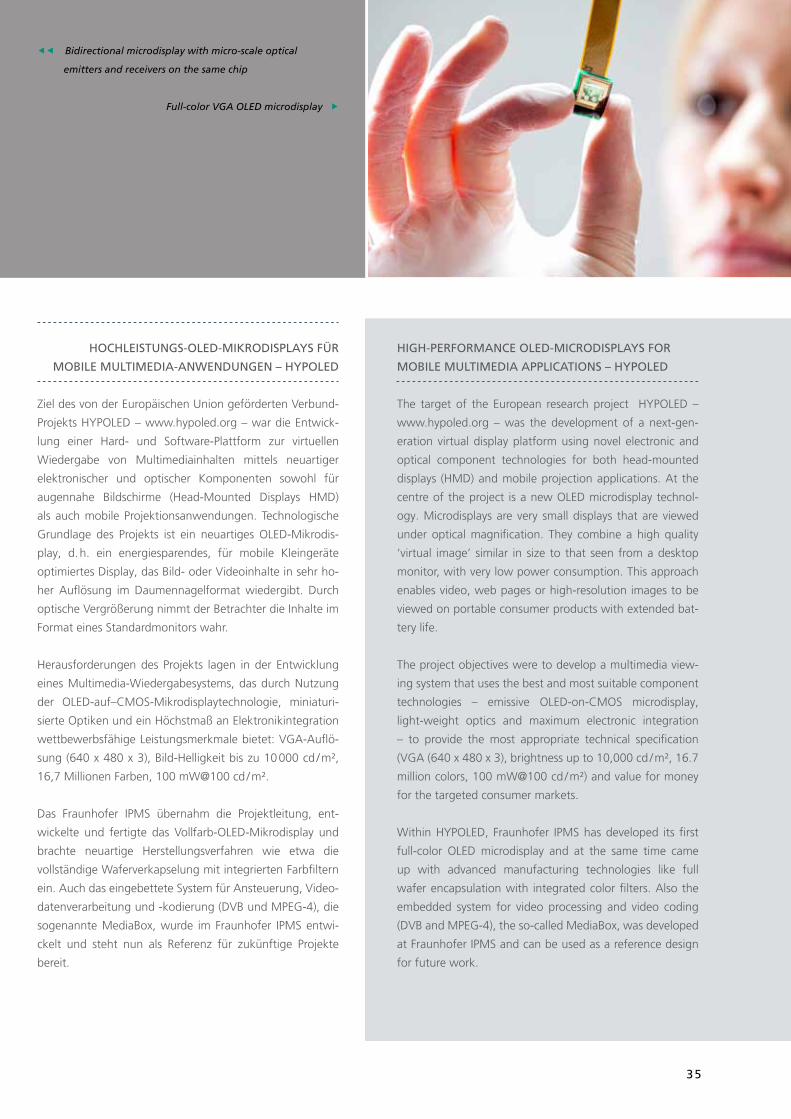
35
hIgh-PerForMance oled-MIcrodIsPlays For
MobIle MultIMedIa aPPlIcatIons – hyPoled
The target of the European research project HYPOLED –
www.hypoled.org – was the development of a next-gen-
eration virtual display platform using novel electronic and
optical component technologies for both head-mounted
displays (HMD) and mobile projection applications. At the
centre of the project is a new OLED microdisplay technol-
ogy. Microdisplays are very small displays that are viewed
under optical magnification. They combine a high quality
‘virtual image’ similar in size to that seen from a desktop
monitor, with very low power consumption. This approach
enables video, web pages or high-resolution images to be
viewed on portable consumer products with extended bat-
tery life.
The project objectives were to develop a multimedia view-
ing system that uses the best and most suitable component
technologies – emissive OLED-on-CMOS microdisplay,
light-weight optics and maximum electronic integration
– to provide the most appropriate technical specification
(VGA (640 x 480 x 3), brightness up to 10,000 cd / m², 16.7
million colors, 100 mW@100 cd / m²) and value for money
for the targeted consumer markets.
Within HYPOLED, Fraunhofer IPMS has developed its first
full-color OLED microdisplay and at the same time came
up with advanced manufacturing technologies like full
wafer encapsulation with integrated color filters. Also the
embedded system for video processing and video coding
(DVB and MPEG-4), the so-called MediaBox, was developed
at Fraunhofer IPMS and can be used as a reference design
for future work.
hochleIstungs-oled-MIkrodIsPlays Für
MobIle MultIMedIa-anwendungen – hyPoled
Ziel des von der Europäischen Union geförderten Verbund-
Projekts HYPOLED – www.hypoled.org – war die Entwick-
lung einer Hard- und Software-Plattform zur virtuellen
Wiedergabe von Multimediainhalten mittels neuartiger
elektronischer und optischer Komponenten sowohl für
augennahe Bildschirme (Head-Mounted Displays HMD)
als auch mobile Projektionsanwendungen. Technologische
Grundlage des Projekts ist ein neuartiges OLED-Mikrodis-
play, d. h. ein energiesparendes, für mobile Kleingeräte
optimiertes Display, das Bild- oder Videoinhalte in sehr ho-
her Auflösung im Daumennagelformat wiedergibt. Durch
optische Vergrößerung nimmt der Betrachter die Inhalte im
Format eines Standardmonitors wahr.
Herausforderungen des Projekts lagen in der Entwicklung
eines Multimedia-Wiedergabesystems, das durch Nutzung
der OLED-auf–CMOS-Mikrodisplaytechnologie, miniaturi-
sierte Optiken und ein Höchstmaß an Elektronikintegration
wettbewerbsfähige Leistungsmerkmale bietet: VGA-Auflö-
sung (640 x 480 x 3), Bild-Helligkeit bis zu 10 000 cd / m²,
16,7 Millionen Farben, 100 mW@100 cd / m².
Das Fraunhofer IPMS übernahm die Projektleitung, ent-
wickelte und fertigte das Vollfarb-OLED-Mikrodisplay und
brachte neuartige Herstellungsverfahren wie etwa die
vollständige Waferverkapselung mit integrierten Farbfiltern
ein. Auch das eingebettete System für Ansteuerung, Video-
datenverarbeitung und -kodierung (DVB und MPEG-4), die
sogenannte MediaBox, wurde im Fraunhofer IPMS entwi-
ckelt und steht nun als Referenz für zukünftige Projekte
bereit.
eeBidirectional microdisplay with micro-scale optical
emitters and receivers on the same chip
Full-color VGA OLED microdisplay
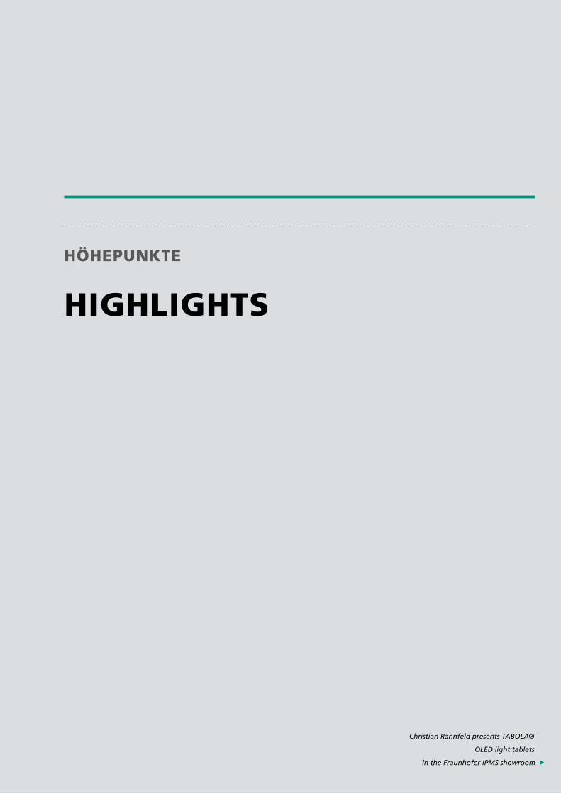
höhePunkte
hIghlIghts
Christian Rahnfeld presents TABOLA®
OLED light tablets
in the Fraunhofer IPMS showroom
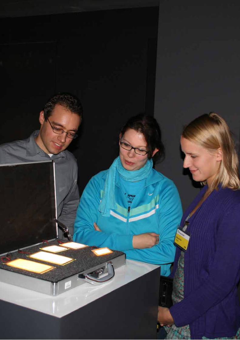
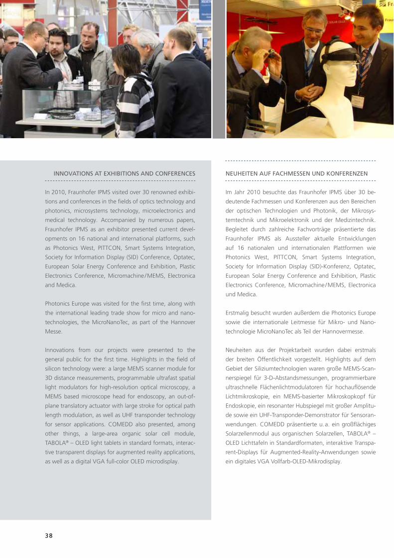
38
neuheIten auF FachMessen und konFerenzen
Im Jahr 2010 besuchte das Fraunhofer IPMS über 30 be-
deutende Fachmessen und Konferenzen aus den Bereichen
der optischen Technologien und Photonik, der Mikrosys-
temtechnik und Mikroelektronik und der Medizintechnik.
Begleitet durch zahlreiche Fachvorträge präsentierte das
Fraunhofer IPMS als Aussteller aktuelle Entwicklungen
auf 16 nationalen und internationalen Plattformen wie
Photonics West, PITTCON, Smart Systems Integration,
Society for Information Display (SID)-Konferenz, Optatec,
European Solar Energy Conference and Exhibition, Plastic
Electronics Conference, Micromachine / MEMS, Electronica
und Medica.
Erstmalig besucht wurden außerdem die Photonics Europe
sowie die internationale Leitmesse für Mikro- und Nano-
technologie MicroNanoTec als Teil der Hannovermesse.
Neuheiten aus der Projektarbeit wurden dabei erstmals
der breiten Öffentlichkeit vorgestellt. Highlights auf dem
Gebiet der Siliziumtechnologien waren große MEMS-Scan-
nerspiegel für 3-D-Abstandsmessungen, programmierbare
ultraschnelle Flächenlichtmodulatoren für hochauflösende
Lichtmikroskopie, ein MEMS-basierter Mikroskopkopf für
Endoskopie, ein resonanter Hubspiegel mit großer Amplitu-
de sowie ein UHF-Transponder-Demonstrator für Sensoran-
wendungen. COMEDD präsentierte u. a. ein großflächiges
Solarzellenmodul aus organischen Solarzellen, TABOLA® –
OLED Lichttafeln in Standardformaten, interaktive Transpa-
rent-Displays für Augmented-Reality-Anwendungen sowie
ein digitales VGA Vollfarb-OLED-Mikrodisplay.
InnoVatIons at exhIbItIons and conFerences
In 2010, Fraunhofer IPMS visited over 30 renowned exhibi-
tions and conferences in the fields of optics technology and
photonics, microsystems technology, microelectronics and
medical technology. Accompanied by numerous papers,
Fraunhofer IPMS as an exhibitor presented current devel-
opments on 16 national and international platforms, such
as Photonics West, PITTCON, Smart Systems Integration,
Society for Information Display (SID) Conference, Optatec,
European Solar Energy Conference and Exhibition, Plastic
Electronics Conference, Micromachine / MEMS, Electronica
and Medica.
Photonics Europe was visited for the first time, along with
the international leading trade show for micro and nano-
technologies, the MicroNanoTec, as part of the Hannover
Messe.
Innovations from our projects were presented to the
general public for the first time. Highlights in the field of
silicon technology were: a large MEMS scanner module for
3D distance measurements, programmable ultrafast spatial
light modulators for high-resolution optical microscopy, a
MEMS based microscope head for endoscopy, an out-of-
plane translatory actuator with large stroke for optical path
length modulation, as well as UHF transponder technology
for sensor applications. COMEDD also presented, among
other things, a large-area organic solar cell module,
TABOLA® – OLED light tablets in standard formats, interac-
tive transparent displays for augmented reality applications,
as well as a digital VGA full-color OLED microdisplay.
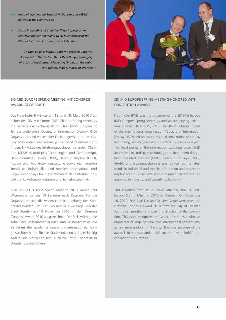
39
sId MId euroPe sPrIng MeetIng honored wIth
conVentIon award
Fraunhofer IPMS was the organizer of the SID Mid Europe
(ME) Chapter Spring Meetings and accompanying exhibi-
tion on March 18 and 19, 2010. The SID-ME Chapter is part
of the international organization “Society of Information
Display” (SID) and holds professional conventions on display
technology, which take place in Central Europe twice a year.
The focal points of the information exchange were OLED
and MEMS microdisplay technology and instrument design,
head-mounted displays (HMD), head-up displays (HUD),
flexible and pico-projection systems, as well as the latest
trends in individual and mobile information and projection
displays for future markets in entertainment electronics, the
automobile industry, and security technology.
180 scientists from 19 countries attended the SID MID
Europe Spring Meeting 2010 in Dresden. On November
10, 2010, Prof. Karl Leo and Dr. Uwe Vogel were given the
Dresden Congress Award 2010 from the City of Dresden
for the organization and scientific direction of the conven-
tion. This prize recognizes the work of scientists who, as
organizers of large national and international conventions,
act as ambassadors for the city. The dual purpose of the
award is to motivate and provide an incentive to hold future
conventions in Dresden.
sId MId euroPe sPrIng MeetIng MIt congress
award gewürdIgt
Das Fraunhofer IPMS war am 18. und 19. März 2010 Aus-
richter des SID Mid Europe (ME) Chapter Spring Meetings
mit begleitender Fachausstellung. Das SID-ME Chapter ist
Teil der weltweiten »Society of Information Display« (SID)
Organisation und veranstaltet Fachkongresse rund um Dis-
playtechnologien, die zweimal jährlich in Mitteleuropa statt-
finden. Im Fokus des Erfahrungsaustauschs standen OLED-
und MEMS-Mikrodisplay-Technologien und Gerätedesign,
Head-mounted Displays (HMD), Head-up Displays (HUD),
flexible und Pico-Projektionssysteme sowie die neuesten
Trends bei individuellen und mobilen Informations- und
Projektionsdisplays für Zukunftsmärkte der Unterhaltungs-
elektronik, Automobilindustrie und Sicherheitstechnik.
Zum SID MID Europe Spring Meeting 2010 kamen 180
Wissenschaftler aus 19 Ländern nach Dresden. Für die
Organisation und die wissenschaftliche Leitung des Kon-
gresses wurden Prof. Karl Leo und Dr. Uwe Vogel von der
Stadt Dresden am 10. November 2010 mit dem Dresden
Congress Award 2010 ausgezeichnet. Der Preis würdigt die
Arbeit der Wissenschaftlerinnen und Wissenschaftler, die
als Veranstalter großer nationaler und internationaler Kon-
gresse Botschafter für die Stadt sind, und soll gleichzeitig
Anreiz und Motivation sein, auch zukünftig Kongresse in
Dresden durchzuführen.
eeHead of engineering Michael Müller presents MEMS
devices at the Hanover Fair
e Saxon Prime Minister Stanislav Tillich inspects an in-
teractive augmented reality OLED microdisplay at the
Plastic Electronics Conference and Exhibition
Dr. Uwe Vogel is happy about the Dresden Congress
Award 2010. On the left: Dr. Bettina Bunge, managing
director of the Dresden Marketing GmbH; on the right:
Dirk Hilbert, deputy mayor of Dresden
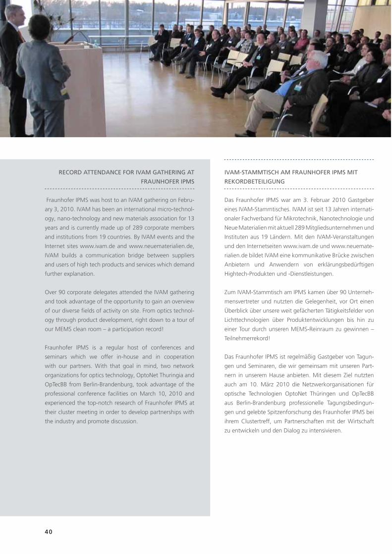
40
record attendance For IVaM gatherIng at
FraunhoFer IPMs
Fraunhofer IPMS was host to an IVAM gathering on Febru-
ary 3, 2010. IVAM has been an international micro-technol-
ogy, nano-technology and new materials association for 13
years and is currently made up of 289 corporate members
and institutions from 19 countries. By IVAM events and the
Internet sites www.ivam.de and www.neuematerialien.de,
IVAM builds a communication bridge between suppliers
and users of high tech products and services which demand
further explanation.
Over 90 corporate delegates attended the IVAM gathering
and took advantage of the opportunity to gain an overview
of our diverse fields of activity on site. From optics technol-
ogy through product development, right down to a tour of
our MEMS clean room – a participation record!
Fraunhofer IPMS is a regular host of conferences and
seminars which we offer in-house and in cooperation
with our partners. With that goal in mind, two network
organizations for optics technology, OptoNet Thuringia and
OpTecBB from Berlin-Brandenburg, took advantage of the
professional conference facilities on March 10, 2010 and
experienced the top-notch research of Fraunhofer IPMS at
their cluster meeting in order to develop partnerships with
the industry and promote discussion.
IVaM-staMMtIsch aM FraunhoFer IPMs MIt
rekordbeteIlIgung
Das Fraunhofer IPMS war am 3. Februar 2010 Gastgeber
eines IVAM-Stammtisches. IVAM ist seit 13 Jahren internati-
onaler Fachverband für Mikrotechnik, Nanotechnologie und
Neue Materialien mit aktuell 289 Mitgliedsunternehmen und
Instituten aus 19 Ländern. Mit den IVAM-Veranstaltungen
und den Internetseiten www.ivam.de und www.neuemate-
rialien.de bildet IVAM eine kommunikative Brücke zwischen
Anbietern und Anwendern von erklärungsbedürftigen
Hightech-Produkten und -Dienstleistungen.
Zum IVAM-Stammtisch am IPMS kamen über 90 Unterneh-
mensvertreter und nutzten die Gelegenheit, vor Ort einen
Überblick über unsere weit gefächerten Tätigkeitsfelder von
Lichttechnologien über Produktentwicklungen bis hin zu
einer Tour durch unseren MEMS-Reinraum zu gewinnen –
Teilnehmerrekord!
Das Fraunhofer IPMS ist regelmäßig Gastgeber von Tagun-
gen und Seminaren, die wir gemeinsam mit unseren Part-
nern in unserem Hause anbieten. Mit diesem Ziel nutzten
auch am 10. März 2010 die Netzwerkorganisationen für
optische Technologien OptoNet Thüringen und OpTecBB
aus Berlin-Brandenburg professionelle Tagungsbedingun-
gen und gelebte Spitzenforschung des Fraunhofer IPMS bei
ihrem Clustertreff, um Partnerschaften mit der Wirtschaft
zu entwickeln und den Dialog zu intensivieren.
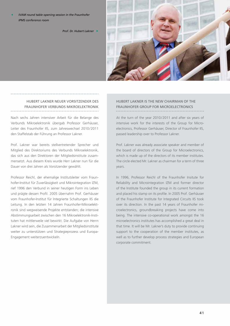
41
hubert lakner Is the new chaIrMan oF the
FraunhoFer grouP For MIcroelectronIcs
At the turn of the year 2010 / 2011 and after six years of
intensive work for the interests of the Group for Micro-
electronics, Professor Gerhäuser, Director of Fraunhofer IIS,
passed leadership over to Professor Lakner.
Prof. Lakner was already associate speaker and member of
the board of directors of the Group for Microelectronics,
which is made up of the directors of its member institutes.
The circle elected Mr. Lakner as chairman for a term of three
years.
In 1996, Professor Reichl of the Fraunhofer Insitute for
Reliability and Microintegration IZM and former director
of the Institute founded the group in its current formation
and placed his stamp on its profile. In 2005 Prof. Gerhäuser
of the Fraunhofer Institute for Integrated Circuits IIS took
over its direction. In the past 14 years of Fraunhofer mi-
croelectronics, groundbreaking projects have come into
being. The intensive co-operational work amongst the 16
microelectronics institutes has accomplished a great deal in
that time. It will be Mr. Lakner’s duty to provide continuing
support to the cooperation of the member institutes, as
well as to further develop process strategies and European
corporate commitment.
e IVAM round table opening session in the Fraunhofer
IPMS conference room
Prof. Dr. Hubert Lakner
hubert lakner neuer VorsItzender des
FraunhoFer Verbunds MIkroelektronIk
Nach sechs Jahren intensiver Arbeit für die Belange des
Verbunds Mikroelektronik übergab Professor Gerhäuser,
Leiter des Fraunhofer IIS, zum Jahreswechsel 2010 / 2011
den Staffelstab der Führung an Professor Lakner.
Prof. Lakner war bereits stellvertretender Sprecher und
Mitglied des Direktoriums des Verbunds Mikroelektronik,
das sich aus den Direktoren der Mitgliedsinstitute zusam-
mensetzt. Aus diesem Kreis wurde Herr Lakner nun für die
Dauer von drei Jahren als Vorsitzender gewählt.
Professor Reichl, der ehemalige Institutsleiter vom Fraun-
hofer-Institut für Zuverlässigkeit und Mikrointegration IZM,
rief 1996 den Verbund in seiner heutigen Form ins Leben
und prägte dessen Profil. 2005 übernahm Prof. Gerhäuser
vom Fraunhofer-Institut für Integrierte Schaltungen IIS die
Leitung. In den letzten 14 Jahren Fraunhofer-Mikroelekt-
ronik sind wegweisende Projekte entstanden; die intensive
Abstimmungsarbeit zwischen den 16 Mikroelektronik-Insti-
tuten hat mittlerweile viel bewirkt. Die Aufgabe von Herrn
Lakner wird sein, die Zusammenarbeit der Mitgliedsinstitute
weiter zu unterstützen und Strategieprozess und Europa-
Engagement weiterzuentwickeln.
42
e Since 1995 the Fraunhofer IPMS is certified
according to ISO 9001
Dr. Christian May and his team get excited about the
award “best development of the year 2010”
dekra audItors Full oF PraIse For Iso 9001
certIFIcatIon
The supervisory audit performed by DEKRA Certification
GmbH on November 2 and 3, 2010 was passed with flying
colors. The auditors were very impressed by how Fraunhofer
IPMS’s Quality Management was enhanced both in form
and method under the management of the newly ap-
pointed Dr. Taut.
Recognition was also given to the integration of production-
relevant documents in the production database system
PRODAB, which strengthens the foundation for effective
and comprehensive data availability and clean room process
control. Further distinction was given to the tools for project
management professionalization developed in 2010, in
particular the annual modular training courses for project
managers, the utilization of milestone trend analyses for the
temporal assessment of project progress, and project evalu-
ation workshops (“Lessons learned”). All of these played a
large part both in making the methodological knowledge
acquired in past projects readily available for future projects,
as well as in helping to identify project risks at an early stage.
Finally, the auditors were especially impressed by the project
„DOPI“, commissioned by Institute management in 2010,
in order to optimize the cycle times in the microsystems
clean room. The aim of this project is to cut the cycle times
in half by 2013. In 2010, technical, organizational and
training measures based on performance indicators and
an availability-synchronization of the production factors
man – machine – material – method were planned and put
into effect. The improvements are already perceptible for
our customers today.
dekra-audItoren Voll des lobes beI
Iso 9001-zertIFIzIerung
Das Überwachungsaudit der DEKRA Certification GmbH
am 2. und 3. November 2010 wurde außerordentlich
erfolgreich bestanden. Die Auditoren würdigten, dass das
Qualitätsmanagement (QM) des Fraunhofer IPMS mit der
Neubesetzung der QM-Leitung durch Frau Dr. Taut inhalt-
lich und methodisch aufgewertet wurde.
Anerkennung fand die Einbindung fertigungsrelevanter
Dokumente in das Produktionsdatenbanksystem PRODAB
als Grundlage für eine effektive und umfassende Daten-
verfügbarkeit und Lenkung der Prozesse im Reinraum.
Weiter wurde hervorgehoben, dass die im Jahr 2010
weiterentwickelten Werkzeuge zur Professionalisierung
des Projektmanagements – speziell die modular aufgebau-
ten, jährlichen Projektleiterschulungen, die Nutzung von
Meilenstein-Trend analysen zur zeitlichen Bewertung von
Projektfortschritten sowie Workshops zur Erfahrungssiche-
rung aus Projekten (»Lessons Learned«) wesentlich dazu
beitragen, das in Projekten akkumulierte Methoden-Wissen
für zukünftige Projekte nutzbar zu machen und Projektrisi-
ken rechtzeitig zu erkennen.
Besonders beeindruckt zeigten sich die Auditoren schließ-
lich vom 2010 im Auftrag der Institutsleitung gestarteten
Projekt »DOPI« zur Optimierung der Durchlaufzeiten im
Mikrosystemreinraum. Ziel des Projekts ist die Halbierung
der Durchlaufzeiten bis 2013. Dazu wurden bereits im
Jahr 2010 auf Kennzahlen basierende technische und
organisatorische Maßnahmen sowie Schulungen und die
Synchronisation der Verfügbarkeit der Fertigungsfaktoren
Mensch – Maschine – Material – Methode konzipiert und
umgesetzt. Die Verbesserungen sind für unsere Kunden
schon heute spürbar.
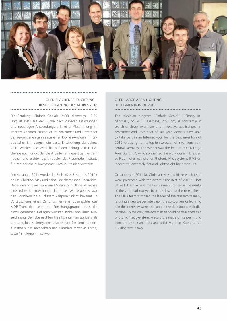
43
oled large area lIghtIng –
best InVentIon oF 2010
The television program “Einfach Genial” (“Simply In-
genious”, on MDR, Tuesdays, 7:50 pm) is constantly in
search of clever inventions and innovative applications. In
November and December of last year, viewers were able
to take part in an Internet vote for the best invention of
2010, choosing from a top ten selection of inventions from
central Germany. The winner was the feature “OLED Large
Area Lighting”, which presented the work done in Dresden
by Fraunhofer Institute for Photonic Microsystems IPMS on
innovative, extremely flat and lightweight light modules.
On January 4, 2011 Dr. Christian May and his research team
were presented with the award “The Best of 2010”. Host
Ulrike Nitzschke gave the team a real surprise, as the results
of the vote had not yet been disclosed to the researchers.
The MDR team surprised the leader of the research team by
feigning a newspaper interview; the co-workers called in to
join the interview were also kept in the dark about their dis-
tinction. By the way, the award itself could be described as a
photonic macro-system: A sculpture made of light-emitting
concrete by the architect and artist Matthias Kothe, a full
18 kilograms heavy.
oled-Flächenbeleuchtung –
beste erFIndung des Jahres 2010
Die Sendung »Einfach Genial« (MDR, dienstags, 19.50
Uhr) ist stets auf der Suche nach cleveren Erfindungen
und neuartigen Anwendungen. In einer Abstimmung im
Internet konnten Zuschauer im November und Dezember
des vergangenen Jahres aus einer Top Ten-Auswahl mittel-
deutscher Erfindungen die beste Entwicklung des Jahres
2010 wählen. Die Wahl fiel auf den Beitrag »OLED Flä-
chenbeleuchtung«, der die Arbeiten an neuartigen, extrem
flachen und leichten Lichtmodulen des Fraunhofer-Instituts
für Photonische Mikrosysteme IPMS in Dresden vorstellte.
Am 4. Januar 2011 wurde der Preis »Das Beste aus 2010«
an Dr. Christian May und seine Forschergruppe überreicht.
Dabei gelang dem Team um Moderatorin Ulrike Nitzschke
eine echte Überraschung, denn das Wahlergebnis war
den Forschern bis zu diesem Zeitpunkt nicht bekannt. In
Vortäuschung eines Zeitungsinterviews überraschte das
MDR-Team den Leiter der Forschungsgruppe; auch die
hinzu gerufenen Kollegen wussten nichts von ihrer Aus-
zeichnung. Den überreichten Preis könnte man übrigens als
photonisches Makrosystem bezeichnen: Ein Leuchtbeton-
Kunstwerk des Architekten und Künstlers Matthias Kothe,
satte 18 Kilogramm schwer.
wIssensManageMent
knowledge ManageMent
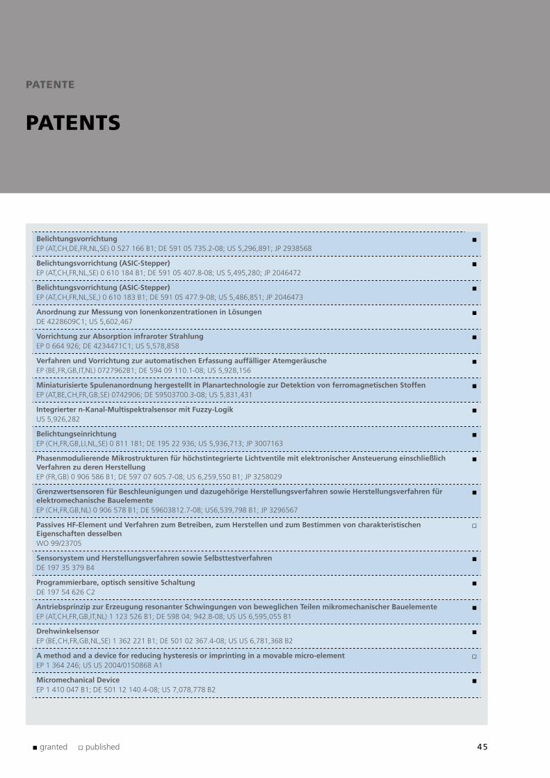
45
BelichtungsvorrichtungEP (AT,CH,DE,FR,NL,SE) 0 527 166 B1; DE 591 05 735.2-08; US 5,296,891; JP 2938568
■
Belichtungsvorrichtung (ASIC-Stepper)EP (AT,CH,FR,NL,SE) 0 610 184 B1; DE 591 05 407.8-08; US 5,495,280; JP 2046472
■
Belichtungsvorrichtung (ASIC-Stepper)EP (AT,CH,FR,NL,SE,) 0 610 183 B1; DE 591 05 477.9-08; US 5,486,851; JP 2046473
■
Anordnung zur Messung von Ionenkonzentrationen in LösungenDE 4228609C1; US 5,602,467
■
Vorrichtung zur Absorption infraroter StrahlungEP 0 664 926; DE 4234471C1; US 5,578,858
■
Verfahren und Vorrichtung zur automatischen Erfassung auffälliger AtemgeräuscheEP (BE,FR,GB,IT,NL) 0727962B1; DE 594 09 110.1-08; US 5,928,156
■
Miniaturisierte Spulenanordnung hergestellt in Planartechnologie zur Detektion von ferromagnetischen StoffenEP (AT,BE,CH,FR,GB,SE) 0742906; DE 59503700.3-08; US 5,831,431
■
Integrierter n-Kanal-Multispektralsensor mit Fuzzy-LogikUS 5,926,282
■
BelichtungseinrichtungEP (CH,FR,GB,LI,NL,SE) 0 811 181; DE 195 22 936; US 5,936,713; JP 3007163
■
Phasenmodulierende Mikrostrukturen für höchstintegrierte Lichtventile mit elektronischer Ansteuerung einschließlich Verfahren zu deren HerstellungEP (FR,GB) 0 906 586 B1; DE 597 07 605.7-08; US 6,259,550 B1; JP 3258029
■
Grenzwertsensoren für Beschleunigungen und dazugehörige Herstellungsverfahren sowie Herstellungsverfahren für elektromechanische BauelementeEP (CH,FR,GB,NL) 0 906 578 B1; DE 59603812.7-08; US6,539,798 B1; JP 3296567
■
Passives HF-Element und Verfahren zum Betreiben, zum Herstellen und zum Bestimmen von charakteristischen Eigenschaften desselbenWO 99/23705
□
Sensorsystem und Herstellungsverfahren sowie SelbsttestverfahrenDE 197 35 379 B4
■
Programmierbare, optisch sensitive SchaltungDE 197 54 626 C2
■
Antriebsprinzip zur Erzeugung resonanter Schwingungen von beweglichen Teilen mikromechanischer BauelementeEP (AT,CH,FR,GB,IT,NL) 1 123 526 B1; DE 598 04; 942.8-08; US US 6,595,055 B1
■
DrehwinkelsensorEP (BE,CH,FR,GB,NL,SE) 1 362 221 B1; DE 501 02 367.4-08; US US 6,781,368 B2
■
A method and a device for reducing hysteresis or imprinting in a movable micro-elementEP 1 364 246; US US 2004/0150868 A1
□
Micromechanical DeviceEP 1 410 047 B1; DE 501 12 140.4-08; US 7,078,778 B2
■
■ granted □ published
Patente
Patents
46
Verfahren zur Verbesserung der Bildqualität und zur Erhöhung der Schreibgeschwindigkeit bei Belichtung lichtempfindlicher SchichtenUS 6,844,916 B2
■
ProjektionsvorrichtungEP (BE,FR,GB,NL) 1 419 411 B1; DE 501 05 156.2; US 6,843,568 B2
■
Method and Apparatus for Controlling Deformable ActuatorsUS 7,424,330
■
SpektrometerEP 1 474 665 B1; DE 502 08 089.2-08; US 7,034,936 B2
■
Device for Protecting a Chip and Method for Operating a ChipEP (DE,NL,SE) 1 499 560 B1
■
Ionensensitiver Feldeffekttransistor und Verfahren zum Herstellen eines ionensensitiven FeldeffekttransistorsEP (CH,FR,GB,SE) 1 436 607 B1; DE 502 02 661.8-08
■
Quasi-Statische Auslenkvorrichtung für SpektrometerEP 1 474 666 B1; DE 502 10 665.4-08; US 7,027,152 B2
■
Mikromechanisches Bauelement mit einstellbarer ResonanzfrequenzEP 1 613 969 B1; DE 503 11 766.8-08
■
Ionensensitiver Feldeffekttransistor und Verfahren zum Herstellen eines ionensensitiven FeldeffekttransistorsEP 1 583 957 B1; DE 502 13 303.1-08; US 7,355,200 B2
■
Aufbringung organischen Materials auf einem SubstratDE 103 12 641 B4
■
Lichtemittierendes Bauelement mit anorganisch-organischer KonverterschichtTW I 242303
■
Method for changing a conversion property of a spectrum conversion layer for a light emitting deviceDE 103 12 679 B4; TW I277362
■
Ionenselektiver Feldeffekttransistor und Verfahren zum Herstellen eines ionensensitiven FeldeffekttransistorsEP (CH) 1 601 957 B1; DE 503 04 800.3-08; US 7,321,143 B2
■
Beschleunigungssensor und Verfahren zum Erfassen einer BeschleunigungEP 1 608 988 B1; DE 503 08 298.8-08; US 7,059,189 B2
■
Verfahren und Anordnung zur Erfassung von Verkehrsdaten mittels Detektion und Klassifikation sich bewegender oder stehender FahrzeugeEP (AT,BE,CH,DE,DK,ES,FR,GR,IT,NL,SE) 1 193 662 B1
■
Method and apparatus for controlling exposure of a surface of a substrateEP (NL) 1 616 211 B1; DE 603 33 398.2; JP 4188322
■
A method to detect a defective elementEP (NL,SE) 1 583 946 B1; DE 60 2004 003 125.9-08; US 7,061,226 B2
■
Optoelektronisches Bauelement mit einer Leuchtdiode und einem LichtsensorEP 1 597 774 B1; DE 503 06 813.6-08
■
Apparatus and Method for Projecting Images and/or Processing MaterialsEP 1 652 377 B1; DE 503 05 392.9-08; US 7,518,770 B2
■
Patente
Patents
47
Leuchtkörper an einer Karosserie eines FahrzeugesDE 10 2004 018 647 A1
□
Verfahren zur hochauflösenden Detektion der Offsetdrift bei resistiven Wheatstone-MeßbrückenEP 1 586 909 B1; DE 50 2005 000 638.0-08; US 7,088,108 B2
■
Display aus organischen Leuchtdioden und Verfahren zu dessen HerstellungTW I248324
■
Hochreflektiv beschichteter mikromechanischer Spiegel, Verfahren zu dessen Herstellung sowie dessen VerwendungUS 7,573,634 B2
■
Vorrichtung und Verfahren zum Ansteuern einer organischen LeuchtdiodeTW I326065
■
Beugungsgitter für elektromagnetische Strahlung sowie Verfahren zur HerstellungEP 1 645 893 A1
□
Vorrichtung und Verfahren zum Erzeugen einer AbbildungDE 10 2004 050 351 B3; US 7,465,051 B2
■
SLM HEIGHT ERROR COMPENSATION METHODEP 1 826 614; WO 2007/096175 A1
□
Vorrichtung zur Reinigung von Innenräumen in VakuumkammernDE 10 2005 025 101 B3
■
Anordnung zum Aufbau eines miniaturisierten Fourier-Transform-Interferometers für optische Strahlung nach dem Michelson- bzw . einem daraus abgeleiteten PrinzipAT 413 765 B; US 7,301,643 B2
■
Optimiertes Verfahren zur Darstellung anellierter, polycyclischer und polyheterocyclischer AromatenDE 10 2005 058 270 B3
■
Vorrichtung zum Ermitteln einer Position eines Lichtstrahls und Verfahren zum Betreiben einer Vorrichtung zum Ermitteln einer Position eines LichtstrahlsDE 10 2005 002 189 B4; CN ZL 2006 1 0006365.0
■
Verfahren zum Herstellen eines Bauelementes mit einem beweglichen AbschnittUS 7,396,740 B2; CN ZL 2006 1 0005939.2
■
Flächiger RöntgendetektorDE 10 2005 012 443 A1
□
Scanner und Verfahren zum Betreiben eines ScannersDE 10 2005 002 190 B4; US 7,469,834 B2; CN ZL 2006 1 0006362.7
■
Verfahren zur Herstellung eines optischen Bauteils mittels oberflächenstrukturierender LaserbearbeitungEP (NL) 1 714 172 B1; DE 10 2004 015 142 B3
■
Mikrooptische AnordnungUS 7,301,690 B2
■
BeleuchtungsvorrichtungDE 10 2005 431 B4; US 7,646,451 B2
■
Semiconductor substrate and methods for the production thereofEP (FR,GB) 1 915 777 B1
■
■ granted □ published
48
Mikromechanisches optisches Element mit einer reflektierenden Fläche sowie dessen VerwendungUS 7,369,288 B2
■
Torsion spring for micromechanical applicationsDE 10 2005 033 801 B4
■
Micro-Optical diffraction grid and process for producing the sameUS 2009/0225424 A1; CN 101273290 A
□
Element zur flächigen BeleuchtungDE 10 2005 050 561 A1
□
Oszillierend auslenkbares mikromechanisches Element und Verfahren zum Betreiben des ElementesUS 2009/0302960 A1; CN 101460392 A
□
Substrat, das zumindest bereichsweise an einer Oberfläche mit einer Beschichtung eines Metalls versehen ist, sowie dessen VerwendungDE 10 2005 048 774 B4
■
Fourier transform spectrometerUS 7,733,493 B2
■
Micromechanical element which can be deflectedUS 2008/0284078 A1; CN 101316789 A
□
Vorrichtung und Verfahren zur Herstellung von Licht emittierenden Elementen mit organischen VerbindungenDE 10 2005 054 609 B4
■
Torsionsfederelement für die Aufhängung auslenkbarer mikromechanischer ElementeCN 101426717 A
□
Auslenkbares mikromechanisches System sowie dessen VerwendungUS 7,841,242 B2
■
Mikromechanisches BauelementDE 10 2006 036 499 B4
■
Microoptic reflecting componentUS 7,490,947 B2
■
Zeilenkamera für spektrale BilderfassungDE 10 2006 019 840 B4; US 7,728,973 B2
■
Vorrichtung und Verfahren zur Steuerung oder Regelung eines oszillierend auslenkbaren mikromechanischen ElementsUS 2009/0072769 A1
□
Anordnung von mikromechanischen ElementenWO 2007/140731 A1; US 2009/0310204 A1
□
Optische AnordnungDE 10 2006 030 541 B4
■
Verfahren zur Herstellung flächiger elektromagnetische Strahlung emittierender Elemente mit organischen LeuchtdiodenDE 10 2006 030 536 B3
■
Verfahren zur Ansteuerung einer Passiv-Matrix-Anordnung organischer LeuchtdiodenDE 10 2006 030 539 A1; US 2008/0122371 A1
□
Patente
Patents
49
Verfahren zum Korrigieren der Oberflächenform eines ElementesEP 2 054 750 B1
■
Integrierter Optokoppler mit organischem Lichtemitter und anorganischem PhotodetektorUS 7,626,207 B2
■
Reflexkoppler mit integriertem organischen LichtemitterDE 10 2006 040 790 A1; JP 2008-98617
□
Verfahren zur Kompensation herstellungsbedingt auftretender Abweichungen bei der Herstellung mikromechanischer Elemente und deren VerwendungDE 10 2006 043 388 B3
■
Waschbares Elektronik-Flachsystem mit freien Anschlusskontakten zur Integration in ein textiles Material oder FlexmaterialDE 10 2007 002 323 B4
■
Schutzstruktur für HalbleitersensorenUS 7,728,363 B2
■
System und Verfahren zur Bestimmung des Verankerungszustandes implantierter EndoprothesenDE 10 2006 051 032 A1
□
Vorrichtung und Verfahren zum Häusen mikromechanischer SystemeDE 10 2007 001 518 A1; CN 101234746 A
□
Mikromechanisches Bauelement mit einstellbarer Resonanzfrequenz durch Geometrieänderung und Verfahren zum Betreiben desselbenDE 10 2007 001 516 B3; US 7,830,577 B2; CN ZL200710160893.6
■
Auslenkbare Struktur, mikromechanische Struktur mit derselben und Verfahren zur Einstellung einer mikromechanischen StrukturDE 10 2007 015 726 A1
□
Projektionsvorrichtung zum scannenden ProjizierenCN ZL 2008 1 0083459.7
■
Mikrooptisches Element mit einem Substrat, an dem an einer optisch wirksamen Oberfläche mindestens eine Höhenstufe ausgebildet ist, Verfahren zu seiner Herstellung und VerwendungenDE 10 2006 057 567 B4
■
Mikromechanisches Bauelement, mikromechanisches System, Vorrichtung zum Einstellen einer Empfindlichkeit eines mikromechanischen Bauelements, Verfahren zur Herstellung eines mikromechanischen BauelementsUS 7,679,152 B2
■
Selbstleuchtende VorrichtungDE 10 2005 057 699 A1
□
Dotiertes Halbleitermaterial und dessen VerwendungDE 10 2007 037 905 A1
□
Verfahren zur Erzeugung einer mikromechanischen StrukturDE 10 2008 013 116 A1; CN 101279712 A
□
Mikromechanisches Bauelement mit verkippten ElektrodenkämmenUS 7,466,474 B2
■
■ granted □ published
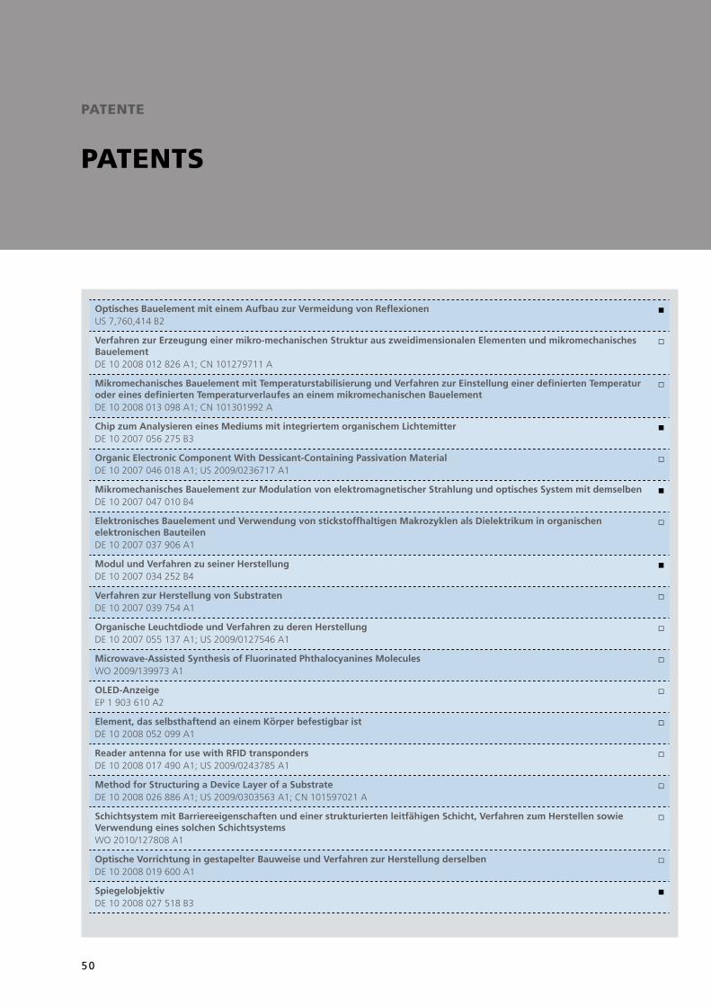
50
Optisches Bauelement mit einem Aufbau zur Vermeidung von ReflexionenUS 7,760,414 B2
■
Verfahren zur Erzeugung einer mikro-mechanischen Struktur aus zweidimensionalen Elementen und mikromechanisches BauelementDE 10 2008 012 826 A1; CN 101279711 A
□
Mikromechanisches Bauelement mit Temperaturstabilisierung und Verfahren zur Einstellung einer definierten Temperatur oder eines definierten Temperaturverlaufes an einem mikromechanischen BauelementDE 10 2008 013 098 A1; CN 101301992 A
□
Chip zum Analysieren eines Mediums mit integriertem organischem LichtemitterDE 10 2007 056 275 B3
■
Organic Electronic Component With Dessicant-Containing Passivation MaterialDE 10 2007 046 018 A1; US 2009/0236717 A1
□
Mikromechanisches Bauelement zur Modulation von elektromagnetischer Strahlung und optisches System mit demselbenDE 10 2007 047 010 B4
■
Elektronisches Bauelement und Verwendung von stickstoffhaltigen Makrozyklen als Dielektrikum in organischen elektronischen BauteilenDE 10 2007 037 906 A1
□
Modul und Verfahren zu seiner HerstellungDE 10 2007 034 252 B4
■
Verfahren zur Herstellung von SubstratenDE 10 2007 039 754 A1
□
Organische Leuchtdiode und Verfahren zu deren HerstellungDE 10 2007 055 137 A1; US 2009/0127546 A1
□
Microwave-Assisted Synthesis of Fluorinated Phthalocyanines MoleculesWO 2009/139973 A1
□
OLED-AnzeigeEP 1 903 610 A2
□
Element, das selbsthaftend an einem Körper befestigbar istDE 10 2008 052 099 A1
□
Reader antenna for use with RFID transpondersDE 10 2008 017 490 A1; US 2009/0243785 A1
□
Method for Structuring a Device Layer of a SubstrateDE 10 2008 026 886 A1; US 2009/0303563 A1; CN 101597021 A
□
Schichtsystem mit Barriereeigenschaften und einer strukturierten leitfähigen Schicht, Verfahren zum Herstellen sowie Verwendung eines solchen SchichtsystemsWO 2010/127808 A1
□
Optische Vorrichtung in gestapelter Bauweise und Verfahren zur Herstellung derselbenDE 10 2008 019 600 A1
□
SpiegelobjektivDE 10 2008 027 518 B3
■
Patente
Patents
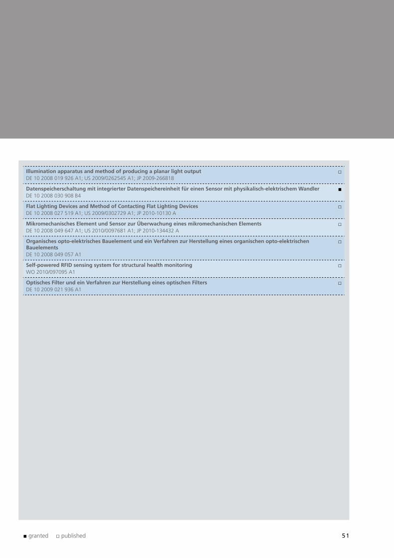
51
Illumination apparatus and method of producing a planar light outputDE 10 2008 019 926 A1; US 2009/0262545 A1; JP 2009-266818
□
Datenspeicherschaltung mit integrierter Datenspeichereinheit für einen Sensor mit physikalisch-elektrischem WandlerDE 10 2008 030 908 B4
■
Flat Lighting Devices and Method of Contacting Flat Lighting DevicesDE 10 2008 027 519 A1; US 2009/0302729 A1; JP 2010-10130 A
□
Mikromechanisches Element und Sensor zur Überwachung eines mikromechanischen ElementsDE 10 2008 049 647 A1; US 2010/0097681 A1; JP 2010-134432 A
□
Organisches opto-elektrisches Bauelement und ein Verfahren zur Herstellung eines organischen opto-elektrischen BauelementsDE 10 2008 049 057 A1
□
Self-powered RFID sensing system for structural health monitoringWO 2010/097095 A1
□
Optisches Filter und ein Verfahren zur Herstellung eines optischen FiltersDE 10 2009 021 936 A1
□
■ granted □ published
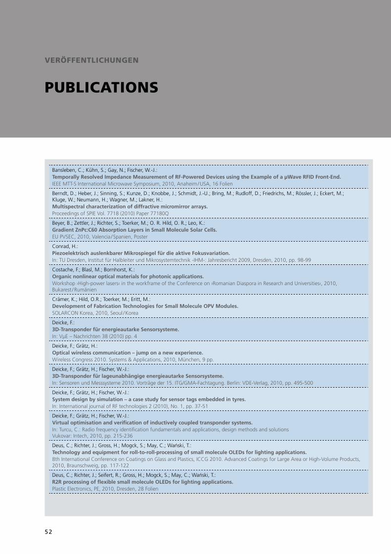
52
veröffentlIchungen
PuBlIcatIons
Bansleben, C.; Kühn, S.; Gay, N.; Fischer, W.-J.:Temporally Resolved Impedance Measurement of RF-Powered Devices using the Example of a μWave RFID Front-End.IEEE MTT-S International Microwave Symposium, 2010, Anaheim / USA, 16 Folien
Berndt, D.; Heber, J.; Sinning, S.; Kunze, D.; Knobbe, J.; Schmidt, J.-U.; Bring, M.; Rudloff, D.; Friedrichs, M.; Rössler, J.; Eckert, M.; Kluge, W.; Neumann, H.; Wagner, M.; Lakner, H.:Multispectral characterization of diffractive micromirror arrays .Proceedings of SPIE Vol. 7718 (2010) Paper 77180Q
Beyer, B.; Zettler, J.; Richter, S.; Toerker, M.; O. R. Hild, O. R.; Leo, K.:Gradient ZnPc:C60 Absorption Layers in Small Molecule Solar Cells .EU PVSEC, 2010, Valencia / Spanien, Poster
Conrad, H.:Piezoelektrisch auslenkbarer Mikrospiegel für die aktive Fokusvariation .In: TU Dresden, Institut für Halbleiter und Mikrosystemtechnik -IHM-: Jahresbericht 2009, Dresden, 2010, pp. 98-99
Costache, F.; Blasl, M.; Bornhorst, K.:Organic nonlinear optical materials for photonic applications .Workshop ›High-power lasers‹ in the workframe of the Conference on ›Romanian Diaspora in Research and Universities‹, 2010, Bukarest / Rumänien
Crämer, K.; Hild, O.R.; Toerker, M.; Eritt, M.:Development of Fabrication Technologies for Small Molecule OPV Modules .SOLARCON Korea, 2010, Seoul / Korea
Deicke, F.:3D-Transponder für energieautarke Sensorsysteme .In: VμE – Nachrichten 38 (2010) pp. 4
Deicke, F.; Grätz, H.:Optical wireless communication – jump on a new experience .Wireless Congress 2010. Systems & Applications, 2010, München, 9 pp.
Deicke, F.; Grätz, H.; Fischer, W.-J.:3D-Transponder für lageunabhängige energieautarke Sensorsysteme .In: Sensoren und Messsysteme 2010. Vorträge der 15. ITG/GMA-Fachtagung. Berlin: VDE-Verlag, 2010, pp. 495-500
Deicke, F.; Grätz, H.; Fischer, W.-J.:System design by simulation – a case study for sensor tags embedded in tyres .In: International journal of RF technologies 2 (2010), No. 1, pp. 37-51
Deicke, F.; Grätz, H.; Fischer, W.-J.:Virtual optimisation and verification of inductively coupled transponder systems.In: Turcu, C.: Radio frequency identification fundamentals and applications, design methods and solutions Vukovar: Intech, 2010, pp. 215-236
Deus, C.; Richter, J.; Gross, H.; Mogck, S.; May, C.; Wański, T.:Technology and equipment for roll-to-roll-processing of small molecule OLEDs for lighting applications .8th International Conference on Coatings on Glass and Plastics, ICCG 2010. Advanced Coatings for Large Area or High-Volume Products, 2010, Braunschweig, pp. 117-122
Deus, C.; Richter, J.; Seifert, R.; Gross, H.; Mogck, S.; May, C.; Wański, T.:R2R processing of flexible small molecule OLEDs for lighting applications.Plastic Electronics, PE, 2010, Dresden, 28 Folien
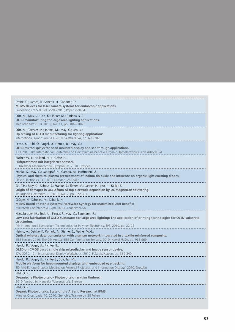
53
Drabe, C.; James, R.; Schenk, H.; Sandner, T.:MEMS devices for laser camera systems for endoscopic applications .Proceedings of SPIE Vol. 7594 (2010) Paper 759404
Eritt, M.; May, C.; Leo, K.; Törker, M.; Radehaus, C.:OLED manufacturing for large area lighting applications .Thin solid films 518 (2010), No. 11, pp. 3042-3045
Eritt, M.; Toerker, M.; Jahnel, M.; May, C.; Leo, K.:Up-scaling of OLED manufacturing for lighting applications .International symposium SID, 2010, Seattle / USA, pp. 699-702
Fehse, K.; Hild, O.; Vogel, U.; Herold, R.; May, C.:OLED microdisplays for head mounted display and see-through applications .ICEL 2010. 8th International Conference on Electroluminescence & Organic Optoelectronics, Ann Arbor / USA
Fischer, W.-J.; Holland, H.-J.; Grätz, H.:Hüftprothesen mit integrierter Sensorik .3. Dresdner Medizintechnik-Symposium, 2010, Dresden
Franke, S.; May, C.; Landgraf, H.; Campo, M.; Hoffmann, U.:Physical and chemical plasma pretreatment of indium tin oxide and influence on organic light emitting diodes.Plastic Electronics, PE, 2010, Dresden, 26 Folien
Gil, T.H.; May, C.; Scholz, S.; Franke, S.; Törker, M.; Lakner, H.; Leo, K.; Keller, S.:Origin of damages in OLED from Al top electrode deposition by DC magnetron sputtering .In: Organic Electronics 11 (2010), No. 2, pp. 322-331
Grüger, H.; Scholles, M.; Schenk, H.:MEMS-Based Photonic Systems: Hardware Synergy for Maximized User BenefitsMicrotech Conference & Expo, 2010, Anaheim / USA
Hasselgruber, M.; Todt, U.; Finger, F.; May, C.; Baumann, R.:Low-cost fabrication of OLED-substrates for large-area lighting: The application of printing technologies for OLED-substrate structuring .4th International Symposium Technologies for Polymer Electronics, TPE, 2010, pp. 22-25
Heinig, A.; Deicke, F.; Kunadt, A.; Starke, E.; Fischer, W.-J.:Optical wireless data transmission with a sensor network integrated in a textile-reinforced composite .IEEE Sensors 2010: The 9th Annual IEEE Conference on Sensors, 2010, Hawaii / USA, pp. 965-969
Herold, R.; Vogel, U.; Richter, B.:OLED-on-CMOS based single chip microdisplay and image sensor device .IDW 2010, 17th International Display Workshops, 2010, Fukuoka / Japan, pp. 339-340
Herold, R.; Vogel, U.; Richter,B.; Scholles, M.:Mobile platform for head-mounted displays with embedded eye-tracking .SID Mid-Europe Chapter Meeting on Personal Projection and Information Displays, 2010, Dresden
Hild, O. R.:Organische Photovoltaic – Photovoltaicmarkt im Umbruch .2010, Vortrag im Haus der Wissenschaft, Bremen
Hild, O. R.:Organic Photovoltaics: State of the Art and Research at IPMS .Minatec Crossroads ’10, 2010, Grenoble / Frankreich, 28 Folien
54
veröffentlIchungen
PuBlIcatIons
Hild, O. R.; Wöhrle, D.; Schnurpfeil, G.:Photovoltaik mit aktiven organischen Materialien – Solarzellen-Markt im Umbruch .In: impulse 1 (2010), pp. 14-17
Jung, D.:Quasistatischer Mikroscanner mit vertikalen Kammantrieben als System-in-Package .In: TU Dresden, Institut für Halbleiter und Mikrosystemtechnik -IHM-: Jahresbericht 2009, Dresden, 2010, pp. 100-101
Kade, J.; Schenk, H.; Müller, M.:MEMS Technologies Dresden – Technology Development, Pilot-Fabrication and Foundry Services .HannoverMesse, 2010, Hannover, Vortrag
Kenda, A.; Kraft, A.; Tortschanoff, A.; Wagner, C.; Lendl, B.; Sandner, T.; Schenk, H.:Miniaturized MEMS-based spectrometric sensor for process control and analysis of carbonated beverages .Proceedings of SPIE Vol. 7594 (2010) Paper 75940U
Kim, Y. H.; Sachse, C.; Hild, O. R.; May, C.; Müller-Meskamp, L.; Leo, K.:Highly Conductive PEDOT:PSS electrodes for Organic Solar Cells .Plastic Electronics, 2010, Dresden, Vortrag
Kirchner, R.; Adolphi, B.; Landgraf, R.; Fischer, W.-J.; Behringer, U. F.W.; Maurer, W.:Antisticking layers on antireflective chromium for hybrid (CNP) nanoimprint molds.Proceedings of SPIE Vol. 7545 (2010) Paper 75450U
Kluge, A.; Gueldner, H.; Reifegerste, F.; Wendt, S.; May, C.:Power electronics in railway lighting systems .IEEE International Conference on Industrial Technology, ICIT, 2010, Viña del Mar, Chile, pp. 793-799
Kunadt, A.; Heinig, A.; Starke, E.; Pfeifer, G.; Cherif, C.; Fischer, W.-J.:Design and properties of a sensor network embedded in thin fiber-reinforced composites.IEEE Sensors 2010: The 9th Annual IEEE Conference on Sensors, 2010, Hawaii / USA, pp. 673-677
Marschner, U.; Fischer, W.-J.; Jettkant, B.; Ruwisch, D.; Grätz, H.; Woldt, G.; Clasbrummel, B.:Anregung und drahtlose Lock-in-Messung von Hüftprothesenschwingungen zur Lockerungsdetektion .In: Technisches Messen: TM 77 (2010), No. 2, pp. 74-82
May, C.:Flexible OLED für Beleuchtungsanwendungen .11. Wörlitzer Workshop ›Anforderungen an Schichten auf flexiblen Substraten für Barriereschutz und weitergehende Eigenschaften‹, 2010, Wörlitz
May, C.:OLEDs von der Rolle – Traum oder Realität?142. Wissenschaftliches Seminar der Fakultät Elektrotechnik an der HTW Dresden, 2010, Vortrag
May, C.:OLED-Lighting at Fraunhofer IPMS / COMEDD .21st Working Group Meeting of the OE-A Dresden, 2010, Dresden
May, C.:Organic and flexible electronics in Germany – a snapshot.National Academies Symposium ›Flexible Electronics for Security, Manufacturing, and Growth‹, 2010, Washington / USA
May, C.:Process Technologies for Advanced Organic Electronic Devices: Microdisplays, Lighting and Solar Cells, Innovations for IndustryHannover Messe / MicroNanoTec, 2010, Hannover
55
May, C.:Project HYPOLED – High-Performance OLED-Microdisplays for HMDs and Projection .OLEDs World Summit 2010, San Francisco / USA
May, C.:Roll-to-Roll Processing for Small Molecule OLED Lighting Devices .OLEDs World Summit 2010, San Francisco / USA
May, C.:Roll-to-Roll Processing of Small Molecule OLED for Lighting Applications .IWFPE 2010 – International Workshop on Flexible & Printable Electronics, 2010, Muju Resort / Korea
May, C.; Fehse, C.; Schmidt, C.; Vogel, U.; Hild, O.R.:Challenges for OLED-on-CMOS process technology .SID Mid-Europe Chapter Meeting on Personal Projection and Information Displays, 2010, Dresden
May, C.; Mogck, S.:COMEDD – Center for Organic Materials and Electronic Devices .Institutsseminar des Fraunhofer FEP, 2010, Dresden, Vortrag
May, C.; Philipp, A.:Laser patterning for OLED substrate preparation .ISL 2010. 3rd International Symposium on Laser-Micromachining, 2010, Chemnitz
Mogck, S.; May, C.:OLED for lighting – R2R fabrication and inspection .pro flex 2010, Dresden, Vortrag, 20 Folien
Mogck, S.; May, C.:Roll-to-roll process line for OLED lighting .11th Coatema International Coating Symposium: Coatema Coating and Laminating, 2010, Dormagen
Pfeifer, R.; Beyer, B.; Fehse, K.; Hild, O.R.; Leo, K.:Simulation of outcoupling efficiencies of OLEDs.Frühjahrstagung des Arbeitskreises Festkörperphysik, 2010, Regensburg, 1 Folie
Philipp, A.; Hasselgruber, M.; Hild, O.R.; May, C.:Substratstrukturierung für organische Leuchtdioden mittels Siebdruck .Technologie-Tag Siebdruck, 2010, Landshut
Rahnfeld, C.; Philipp, A.; Hasselgruber, M.; Hild, O.R.; May, C.:Substrate patterning for organic electronic devices at Fraunhofer IPMS .Plastic Electronics, PE 2010, October 19-21, 2010, Dresden, 21 Folien
Ruppel, L.; May, C.:TCOs für OLED .OTTI-Fachtagung Transparent leitfähige Schichten, 2010, Neu-Ulm
Sandner, T.; Grasshoff, T.; Wildenhain, M.; Schenk, H.:Synchronized microscanner array for large aperture receiver optics of LIDAR systems .Proceedings of SPIE Vol. 7594 (2010) Paper 75940C
Sandner, T.; Wildenhain, M.; Gerwig, C.; Schenk, H.; Schwarzer, S.; Wölfelschneider, H.:Large aperture MEMS scanner module for 3D distance measurement .Proceedings of SPIE Vol. 7594 (2010) Paper 75940D
56
veröffentlIchungen
PuBlIcatIons
Scade, A.; Günther, S.; Grätz, H.; Holland, H.-J.:Sophisticated nvSRAM based transponder architecture provides novel features for field programming and safety.Dresdner Arbeitstagung Schaltungs- und Systementwurf, DASS 2010, Dresden, pp. 103-109
Schmidt, C.:Verkapselungstechnologie für nanophotonische Bauelemente auf Basis von organischen Leuchtdioden (OLED) .In: TU Dresden, Institut für Halbleiter und Mikrosystemtechnik -IHM-: Jahresbericht 2009, Dresden, 2010, pp. 102-103
Schmidt, J.-U.;. Bring, M.; Heber, J.; Friedrichs, M.; Rudloff, D.; Rößler, J.; Berndt, D.; Neumann, H.; Kluge, W.; Eckert, M.; List, M.;. Müller, M.; Wagner, M.:Technology development of diffractive micromirror arrays for the deep ultraviolet to the near infrared spectral range .Proceedings of SPIE Vol. 7716 (2010) Paper 77162L
Scholles, M.; Grafe, M.; Miskowiec, P.; Bock, V.; Schenk, H.:Optical inspection of MOEMS devices using a configurable and suitable for production image processing system.Proceedings of SPIE Vol. 7592 (2010) Paper 75920L
Scholles, M.; Kroker, L.; Vogel, U.; Krüger, J.; Walczakc, R.; Ruano-Lopez, J.:LABONFOIL: Investigations regarding microfluidic skin patches for drug detection using flexible OLEDs.Proceedings of SPIE Vol. 7593 (2010) Paper 75930C
Scholles, M.; Vogel, U.:OLED-on-CMOS for sensors and microdisplays .CMOS Emerging Technologies Workshop, 2010, Whistler / Kanada, 20 Folien
Scholles, M.; Vogel, U.; Amelung, J.; May, C.:Integration of organic light emitting diodes into CMOS circuits for smart optoelectronic systems .Smart systems integration 2010. 4th European Conference & Exhibition on Integration Issues of Miniaturized Systems – MEMS, MOEMS, ICs and Electronic Components, 2010, Como / Italien, Paper 33, 8 pp.
Scholles, M.; Vogel, U.; Underwood, I.; Notni, G.; Zilstorff, C.; Meerholz, K.; Haas, G.:HYPOLED – high-performance OLED microdisplays for mobile multimedia HMD and projection applications .International symposium SID, 2010, Seattle / USA, pp. 1926-1929
Schütze, F.; Hild, O.R.; Philipp, A.; Richter, S.:Structuring of TCO-coated barrier foils for flexible organic solar cells.EU PVSEC, 2010, Valencia / Spanien, Poster
Seidl, K.; Knobbe, J.; Lakner, H.:Design für ein Zoomobjektiv mit deformierbaren Spiegeln .DGaO Proceedings, 111. Tagung, 2010, Wetzlar, Vortrag B12
Seidl, K.; Knobbe, J.; Schneider, D.; Lakner, H.:Distortion correction of all-reflective unobscured optical-power zoom objective.In: Applied optics 49 (2010), No. 14, pp. 2712-2719
Szyszka, B.; Löbmann, P.; Georg, A.; May, C.; Elsässer, C.:Development of new transparent conductors and device applications utilizing a multidisciplinary approach .In: Thin solid films 518 (2010), No. 11, pp. 3109-3114
Szyszka, B.; May, C.; Götzendörfer, S.; Ulrich, S.; Polenzky, C.; Ruppel, L.; Thomas, M.; Klages, C.-P.; Löbmann, P.:Patterned deposition of transparent and conductive layers – new pathways towards cost efficient manufacturing techniques.Printed Electronics & Photovoltaics Europe, 2010, Dresden
Toerker, M.; Jahnel, M.; Ruppel, L.; May, C.; Leo, K.:OLED lighting tile preparation on Gen2 deposition tool .Plastic Electronics, PE, 2010, Dresden, 23 Folien
57
Tortschanoff, A.; Lenzhofer, M.; Frank, A.; Wildenhain, M.; Sandner, T.; Schenk, H.; Kenda, A.:Optical position feedback and phase control of MOEMS-scanner mirrors .Proceedings of SPIE Vol. 7594 (2010) Paper 75940K
Tortschanoff, A.; Lenzhofer, M.; Frank, A.; Wildenhain, M.; Sandner, T.; Schenk, H.; Kenda, A.:Position encoding and phase control of resonant MOEMS-mirrors .Eurosensors XXIII, the 23rd Int’l Conference on Solid-State Sensors, Actuators, Microsystems and Nanosystems, 2009, Lausanne / Schweiz In: Sensors and actuators. A, Physical 162. 2010, Nr. 2, pp. 235-240
Tortschanoff, A.; Wildenhain, M.; Sandner, T.; Schenk, H.; Kenda, A.:Position feedback and phase control of resonant MOEMS-mirrors with one and two axes .In: Procedia Engineering 5(2010) pp. 689-692
Türke, A.; Fischer, W.-J.; Adler, H.-J.; Pich, A.:Microwave-assisted synthesis of hybrid colloids for design of conducting films.In: Polymer 51 (2010), No. 21, pp. 4706-4712
Vogel, U.:OLED-on-CMOS: ›Leuchtendes Silizium‹ für Mikrodisplays und Opto-Sensorik .Silicon Saxony Day, Smart Systems Integration Forum, 2010, Dresden
Vogel, U.:Volldigitales VGA Mikrodisplay auf OLED-Basis .In: ElektronikPraxis, 13 (2010), pp. 22-24
Vogel, U.; Herold, R.; Schreiber, P.; Sieler, M.; Voth, S.; Schuchert, T.; Zöllner, M.; Bockholt, U.:iSTAR: Interactive See-Through Augmented-Reality Displays .Fraunhofer Netzwerk Symposium, 2010, Fraunhofer-Gesellschaft, München
Vogel, U.; Kreye, D.; Richter, B.; Fehse, K.; Presberger, T.; Herold, R.; Scholles, M.:OLED microdisplays with advanced features enabling new applications .IMID 2010 Digest, 10th International Meeting on Information Display, Seoul / Korea, pp. 402-403
Vogel, U.; König, P.; Herold, R.; Törker, M.; Fehse, K.; Wahl, J.; Barth,S.:OLED display, driver and microdisplays for automotive use .SID-ME Chapter Fall Meeting 2010. Automotive Displays Applications, Chances and Challenges, 2010, Sindelfingen
Vogel, U.; Richter, B.:OLED-on-CMOS: Highly-efficient embedded organic light emitter for CMOS optoelectronics.IEEE Conference on Micro and Nano Technologies, 2010, Sinaia / Rumänien
Vogel, U.; Richter, B.; Herold, R.; Fehse, K.; Leo, K.:OLED-on-CMOS for microdisplays . Technology, design, applications .Plastic Electronics, PE, 2010, Dresden, 17 Folien
Vogel, U.; Richter, B.; Herold, R.; Kreye, D.; Presberger, T.; Fehse, K.:OLED-on-CMOS: Analog-Design an der Schnittstelle zu OLED- und CMOS-Prozesstechnologie .ANALOG 2010, Entwicklung von Analogschaltungen mit CAE-Methoden, 2010, Erfurt
Vogel, U.; Schreiber, P.; Voth, S.; Zöllner, M.; Herold, R.:iSTAR: Interactive See-Through Augmented Reality Displays .SID Mid-Europe Chapter Meeting on Personal Projection and Information Displays, 2010, Dresden
Vogel, U.; Underwood, I.; Notni, G.; Zilstorff, C.; Meerholz, K.; Haas, G.:HYPOLED: VGA OLED micro-display for HMD and micro-projection .SID Mid-Europe Chapter Meeting on Personal Projection and Information Displays, 2010, Dresden
58
veröffentlIchungen
PuBlIcatIons
Vogel, U.; Underwood, I.; Notni, G.; Zilstorff, C.; Meerholz, K.; Haas, G.:HYPOLED: VGA and WVGA OLED microdisplays for HMD and micro-projection .OLEDs World Summit 2010, San Francisco / USA
Weder, A.:An energy model of the ultra-low-power transceiver nRF24L01 for wireless body sensor networks .2nd Int’l Conference on Computational Intelligence, Communication Systems and Networks, CICSyN, 2010, Liverpool / GB, pp. 118-123
Wullinger, I.; Rudloff, D.; Lukat, K.; Dürr, P.; Krellmann, M.; Kunze, D.; Narayana Samy, A.; Dauderstädt, U.; Wagner, M.:Temperature measurement on MOEMS micromirror plates under illumination .Proceedings of SPIE Vol. 7592 (2010) Paper 75920P
Wöhrle, D.; Hild, O.R.:Organische Solarzellen: Energie der Zukunft .In: Chemie in unserer Zeit 44 (2010), No. 3, pp. 174-189
Zaunseder, S.:Self-organizing maps in ischaemia processing .3. Dresdner Medizintechnik-Symposium, 2010, Dresden, Poster
Zaunseder, S.; Aipperspach, W.; Poll, R.:Discrimination between ischemic and heart-rate related ST-episodes .BIOSTEC 2010, 3rd Int’l Joint Conference on Biomedical Engineering Systems and Technologies, 2010, Valencia / Spanien, pp. 245-251
Zaunseder, S.; Nauber, R.; Poll, R.:Characterizing the scaling behaviour of the ventricular repolarisation .Biosignal 2010, International Biosignal Processing Conference, 2010, Berlin, 4 pp.
Zaunseder, S.; Nauber, R.; Poll, R.:Methodical aspects investigating the dynamics of ventricular repolarization’s morphological characteristics .ESGCO 2010, 6th Conference of the European Study Group on Cardiovascular Oscillations, 2010, Berlin, 4 pp.
59
Dissertations Dissertationen
eritt, Michael Großflächige Abscheidung organischer Leuchtdioden und Nutzung optischer Verfahren zur in situ Prozesskontrolle
Technische Universität Chemnitz
roscher, kai-uwe Mikrosysteme zur Erfassung von Stoßvorgängen in FaserverbundwerkstoffenTechnische Universität Dresden
seidl, kristof Entwicklung eines Systemansatzes für ein Spiegel-Zoomobjektiv mit deformierbaren ElementenTechnische Universität Dresden
türke, alexander Synthese von Silberhybridpartikeln als elektrisch leitfähige Tinten für den Ink-Jet Druck von leitfähigen Strukturen
Technische Universität Dresden
Master Theses Masterarbeiten
baumgarten, Judith Entwicklung eines blickrichtungsgesteuerten Location Based Services für Menschen mit eingeschränkter Mobilität
Brandenburgische Technische Universität Cottbus; Betreuer: Böger, Astrid
Franke, sebastian Charakterisierung von Plasmavorbehandeltem Indiumzinnoxid und dessen Einfluss auf organische Leuchtdioden
Brandenburgische Technische Universität Cottbus; Betreuer: Schenk, Harald
Müller, tilo Schnittstellenprogrammierung einer mobilen Plattform zur Anbindung von HMDs mit bidirektionalen OLED-Mikrodisplays
Hochschule Zittau / Görlitz
Noga, Marcin Bogumił Investigation of dynamic behaviour of advanced micromirror array designs used for particular applications by modelling and simulation using analytical and numerical methods respectively and comparison to experiment
Brandenburgische Technische Universität Cottbus; Betreuer: Schenk, Harald
Pérez, José ramón Martínez Use for OLED in automobile applicationUniversität Granada
steuer, Maik Untersuchung hardwareintegrierter Bildverarbeitungsalgorithmen für ein mobiles Eyetracking-SystemHochschule für Technik und Wirtschaft Dresden
Wański, Tomasz Process setup and optimization for monochrome doped OLEDs in roll-to-roll processingBrandenburgische Technische Universität Cottbus; Betreuer: Mogck, Stefan
zettler, Johannes kristian Optical characterization of organic layers for OLED and OPVC processesHumboldt Universität zu Berlin; Betreuer: Leo, Karl
wIssenschaftlIche arBeIten
acadeMIc theses
60
Diploma Theses Diplomarbeiten
arndt, susann Realisierung eines Mikrofluidiksystems für die BiosensorikOtto-von-Guericke-Universität Magdeburg; Betreuer: Lucklum, R.
henschel, walter-daniel Weiterentwicklung und Evaluierung hardwareintegrierter Bildverarbeitungsalgorithmen für ein mobiles Eyetracking-System
Hochschule für Technik und Wirtschaft Dresden; Betreuer: Herold, Rigo
hofmann, thomas Entwurf und Untersuchung eines 1-GBit-PHY/Framer-Modules für die drahtlose optische Datenübertragung
Technische Universität Dresden; Betreuer: Deicke, Frank; Fischer, Wolf-Joachim
hoppe, daniel Entwicklung und Aufbau eines Messeausstellers für LichtmodulatorenHochschule Mittweida; Betreuer: Sinning, Steffen
kölle, klaus Charakterisierung der Ratenabhängigkeit und Optimierung der Ratenstabilität und Abscheidungshomogenität der VTE-Organikquellen sowie Vergleich mit OVPD-Quellen und einer Linearquelle der COMEDD Gen2 Pilotfertigungslinie
Westsächsische Hochschule Zwickau; Betreuer: Crämer, Konrad
lehmann, claudia Defektcharakterisierung von OLED-Systemen auf flexiblen MetallsubstratenWestsächsische Hochschule Zwickau; Betreuer: Mogck, Stefan
Peschel, Marcel Entwicklung von chemisch-mechanischen Oberflächenbearbeitungsprozessen in MOEM-TechnologienTechnische Universität Dresden; Betreuer: Kunath, Christian
Philipp, andré Herstellung von Substraten für organische Leuchtdioden in DickschichttechnologieTechnische Universität Dresden; Betreuer: Lakner, Hubert; Hasselgruber, Moritz
Przyborowski, Julia Marktanalyse und Konzepterstellung für den Aufbau eines Foundry Services von MEMS ProduktenHochschule für Technik und Wirtschaft Dresden; Betreuer: Walther, Mario
richter, susan Charakterisierung und Optimierung von organischen Solarzellen und deren Hochskalierung von der einzelnen Testzelle zum Solarzellenmodul
Technische Universität Dresden; Betreuer: Lakner, Hubert; Törker, Michael
risse, thomas Farbpunktdetektion auf Basis monolithisch integrierter organischer Leuchtdioden und PhotodiodenHochschule für Technik und Wirtschaft Dresden; Betreuer: Kreye, Daniel
scholz, karsten OLED Ansteuerung mit integrierter Lebensdauerkompensation und Farbsteuerung für Beleuchtungsanwendungen
Technische Universität Dresden; Betreuer: Fischer, Wolf-Joachim; Todt, Ulrich
segieth, steffen Infrarot-Beleuchtung der Augenszene für ein mobiles Eyetracking-SystemHochschule für Technik und Wirtschaft Dresden; Betreuer: Herold, Rigo
spindler, Martin Bewertung optischer drahtloser KommunikationstechnologienTechnische Universität Dresden; Betreuer: Deicke, Frank
tietze, Max l. Simulation und Messung der Strom- und Temperaturverteilung in großflächigen OLEDsTechnische Universität Dresden; Betreuer: Lakner, Hubert; Leo, Karl
uschner, Friedemann Effiziente Algorithmen zur Analyse topographischer Datensätze von MMA-BauelementenTechnische Universität Dresden; Betreuer: Brehm, Ulrich
wartenberg, Philipp Entwurf eines Analog-Digital-Wandlers für ein bidirektionales MikrodisplayTechnische Universität Dresden; Betreuer: Uhlig, Johannes
wIssenschaftlIche arBeIten
acadeMIc theses
61
Bachelor Theses Bachelorarbeiten
Friebel, Felix Konstruktion und Evaluation von HMDs für bidirektionale OLED-MikrodisplaysFachhochschule Lausitz Senftenberg; Betreuer: Herold, Rigo
güth, Frederic Herstellung von flexiblen organischen Bauelementen und Vergleich mit starren SystemenTU Bergakademie Freiberg; Betreuer: Hild, Olaf-Rüdiger
62
anfahrt
how to reach us
strassenVerbIndung
Über die Autobahn A4 an der Anschlußstelle »Dresden-
Flughafen« abfahren. Die Hermann-Reichelt-Straße in
Richtung Hoyerswerda benutzen. Diese mündet in die
Grenzstraße. Die Maria-Reiche-Straße ist die erste Abzwei-
gung rechts nach dem Dörnichtweg.
Vom Zentrum Dresden die B97 in Richtung Hoyerswerda
fahren. Durch das Zentrum des Ortsteils Klotzsche fahren.
400 m nachdem die Straßenbahngleise von der Straßen-
mitte auf die rechte Seite wechseln, zweigt die Grenzstraße
links von der B97 ab. Die Maria-Reiche-Straße zweigt nach
etwa 500 m links ab.
FlugVerbIndung
Nach der Ankunft im Flughafen Dresden entweder den Bus
80 bis zur Haltestelle »Grenzstraße Mitte« am Anfang des
Dörnichtwegs benutzen und noch 150 m der Grenzstraße
folgen oder mit der S-Bahn eine Haltestelle bis Dresden-
Grenzstraße fahren und etwa 400 m die Grenzstraße weiter
laufen.
nahVerkehr
Die Straßenbahn 7 vom Stadtzentrum bis Haltestelle »Ar-
konastraße« benutzen. Dann schräg nach links durch das
Wohngebiet zur Grenzstraße gehen und dieser links folgen.
Die Maria-Reiche-Straße erreichen Sie nach etwa zehn
Minuten Fußweg.
Fahren Sie mit der S-Bahn Linie 2 bis Dresden-Grenzstraße.
Diese entgegengesetzt zur Fahrtrichtung ca. 400 m zurück-
gehen. Die Maria-Reiche-Straße zweigt hier rechts ab.
road connectIon
Follow expressway A4, from exit “Dresden-Flughafen” drive
in direction Hoyerswerda along H.-Reichelt-Straße, which
runs into the Grenzstraße. Maria-Reiche-Straße is the first
road to the right after Dörnichtweg.
From Dresden city on B97 in direction Hoyerswerda.
Grenzstraße branches off to the left 400 m after the tram
rails change from the middle of the street to the right side.
Maria-Reiche-Straße branches off to the left after approxi-
mately 500 m.
FlIght connectIon
After arriving at airport Dresden use either bus 80 to bus
stop “Grenzstraße Mitte” at the beginning of Dörnichtweg
and follow Grenzstraße for 150 m or take city railway
S-Bahn to station Dresden-Grenzstraße and walk about
400 m further along Grenzstraße.
PublIc transPort
Take tram 7 from Dresden city to tram stop “Arkona-
straße”, turn left and cross the residential area diagonally
to Grenzstraße. Follow this road for about 10 min to the left
and you will reach Maria-Reiche-Straße.
Take city railway S-Bahn line 2 to station Dresden-
Grenzstraße. Reverse for ca. 400 m. Maria-Reiche-Straße
branches off to the right.
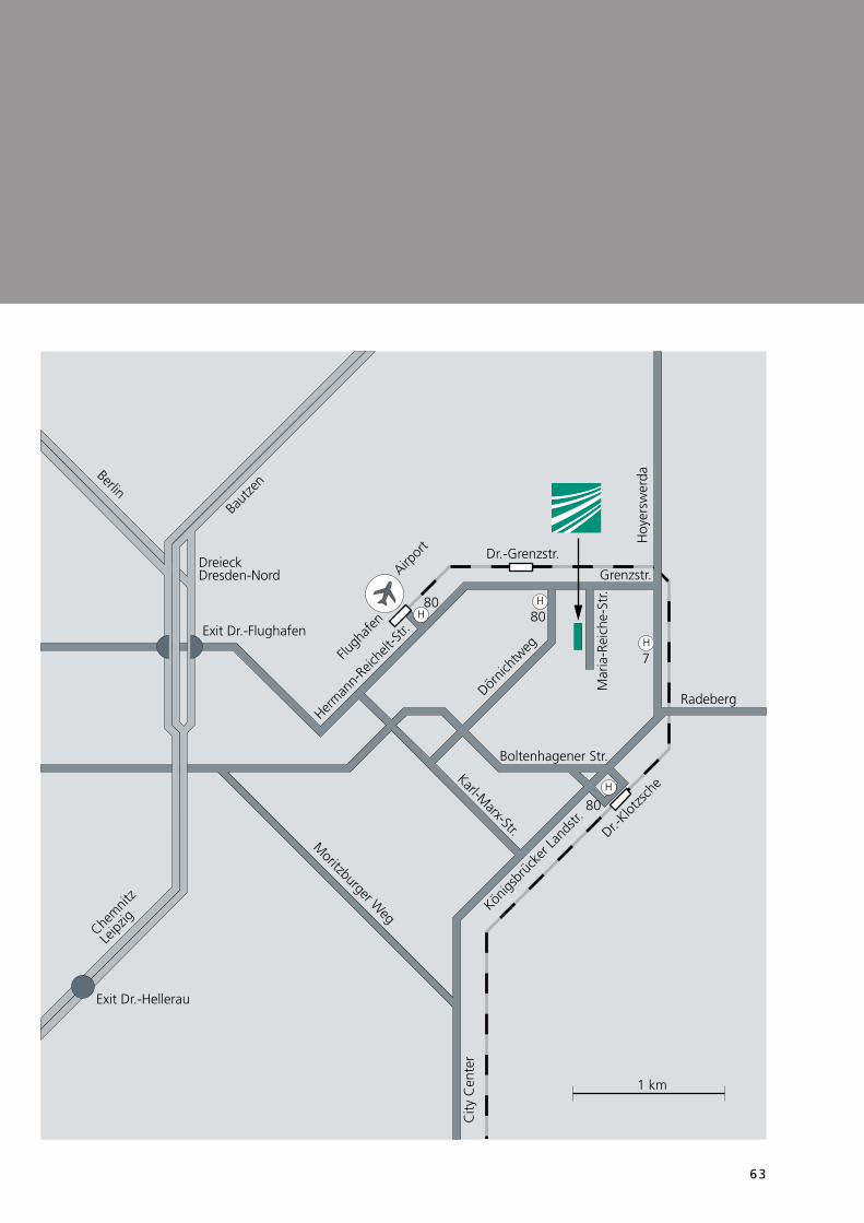
63
H
H
H
Dr.-Grenzstr.
Grenzstr.
Exit Dr.-Flughafen
Berlin
Baut
zen
Dr.-Klot
zsch
e
Flugh
afen
Exit Dr.-Hellerau
Chem
nitz
Leipz
ig
Mar
ia-R
eich
e-St
r.
Radeberg
Hoy
ersw
erda
Karl-Marx-Str.
Herm
ann-
Reich
elt-S
tr.
City
Cen
ter
Königs
brüc
ker L
ands
tr.
Dörnic
htweg
DreieckDresden-Nord
Boltenhagener Str.
1 km
7
80
80
Moritzburger W
eg
Airpor
t
H80
64
MorItz FleIscher
Tel. +49 (0) 3 51 / 88 23 - 2 49
Fax +49 (0) 3 51 / 88 23 - 2 66
Ines schedwIll
Tel. +49 (0) 3 51 / 88 23 - 2 38
Fax +49 (0) 3 51 / 88 23 - 2 66
weItere InforMatIonen
More InforMatIon
© Fraunhofer Institute for Photonic Microsystems IPMS,
Dresden 2011
copyrigHts
All rights reserved. Reproduction requires the permission of
the Director of the Institute.
Layout
Fraunhofer IPMS
transLation
Fraunhofer IPMS; Tara Kneitz, Dresden
Medienhaus Lißner OHG, Dresden
pHotos
Fraunhofer-Gesellschaft; Photographie Jürgen Lösel;
Sven Döring / VISUM; René Gaens Fotografie
© Fraunhofer-Institut für Photonische Mikrosysteme IPMS,
Dresden 2011
recHte
Alle Rechte vorbehalten. Nachdruck nur mit Genehmigung
der Institutsleitung.
gestaLtung
Fraunhofer IPMS
Übersetzung
Fraunhofer IPMS; Tara Kneitz, Dresden
druck
Medienhaus Lißner OHG, Dresden
fotos
Fraunhofer-Gesellschaft; Photographie Jürgen Lösel;
Sven Döring / VISUM; René Gaens Fotografie
impressum
editorial notes

Heading
Text
ÜberscHrift
Text
Jahresbericht
annual report
2010
F R A U N H O F E R I N S T I T U T E F O R p H O T O N I c M I c R O S y S T E M S I p M S