um10389 36 w tld application with uba2014 · document information um10389 36 w tld application with...
TRANSCRIPT

UM1038936 W TLD application with UBA2014Rev. 01 — 2 October 2009 User manual
Document informationInfo ContentKeywords UBA2014, Half bridge driver
Abstract The UBA2014 integrated half bridge driver IC has been designed for driving electronically ballasted fluorescent lamps.The IC provides the drive function for two discrete power MOSFETs.

NXP Semiconductors UM1038936 W TLD application with UBA2014
Revision historyRev Date Description
01 20091002 First issue, replaces application note AN10181
UM10389_1 © NXP B.V. 2009. All rights reserved.
User manual Rev. 01 — 2 October 2009 2 of 16
Contact informationFor more information, please visit: http://www.nxp.com
For sales office addresses, please send an email to: [email protected]

NXP Semiconductors UM1038936 W TLD application with UBA2014
1. Introduction
The UBA2014 integrated half bridge driver IC has been designed for driving electronically ballasted fluorescent lamps. The IC provides the drive function for two discrete power MOSFETs. Besides the drive function the IC also includes a level-shift circuit, an oscillator, a lamp voltage monitor, a current control function a timer function, and protections.
This user manual gives a description of a typical integrated 36 W TLD application. The voltage fed half bridge is supplied by a constant 400 V (DC) supply (either an external or a PFC supply). According IEC61000-3-2 (limits for harmonic current emission), power factor correction for loads over 25 W is required, see Figure 1).
If complying with the IEC61000-3-2 standard is not required, a normal input circuit like in Figure 2, can be used. Keep in mind that the lamp power is not constant over a big input voltage range (e.g. 190 V (AC) to 264 V (AC)). The voltage fed half bridge topology allows for operating easily in Zero Voltage Switching (ZVS) series resonant mode, thus reducing the transistor switching losses and the electromagnetic interference. During the preheat time the UBA2014 controls the current which flows in the filament of the lamp. The preheat timer and control system determine the optimal preheat time and preheat current to make sure the lamp has a long life and an efficient ignition. After the preheat time the lamp must be ignited by reducing the switching frequency, in this way increasing the voltage across it. The IC controls the maximum ignition voltage and the ignition timer determines the maximum ignition time. During this phase the capacitive mode protection ensures a safe operation of the power MOSFETs. In the burn phase the lamp current is controlled by the average current system. In this phase the lamp can be dimmed to a low level by frequency dimming.
The UBA2014 has protections for lamp ageing, lamp failures, and lamp removal. The power-down function can safely switch off the power inverter.
Fig 1. Input circuitry using a PFC
Fig 2. Normal input circuitry
UM10389_1 © NXP B.V. 2009. All rights reserved.
User manual Rev. 01 — 2 October 2009 3 of 16

NXP Semiconductors UM1038936 W TLD application with UBA2014
2. Features
• Integrated half bridge power IC for fluorescent applications– Integrated high side/low side, including bootstrap circuitry– Based on the BCD 650 V power logic technology– Accurate oscillator and timer– Adjustable frequency range (with fixed fmax/fmin ratio)– Adaptive non-overlap time control– Capacitive mode protection– Adjustable preheat current and time control– Single ignition attempt– Power-down function
• Soft start by frequency sweep down from start frequency• Adjustable ignition voltage control• Lamp current control• Down to 10 % dimming• Protection against lamp failures or lamp removal• SO16, DIP16 package
3. General description
3.1 Printed-circuit board
Remark: this controller had no official number.
Fig 3. The printed-circuit board of the UBA2014 application
UM10389_1 © NXP B.V. 2009. All rights reserved.
User manual Rev. 01 — 2 October 2009 4 of 16

NXP Semiconductors UM1038936 W TLD application with UBA2014
3.2 Block diagram
Figure 4 shows the block schematic diagram of the UBA2014. The block state logic forms the heart of the controller and controls all other internal functions. Initial start-up is achieved by means of charging an external capacitor (C15 in Figure 5) connected to pin 7. The state logic will be reset and both outputs GL and GH are set to low (reset state). Reaching a voltage of 13.6 V, the controller enables the blocks voltage controlled oscillator (VCO), the Adaptive Non-overlap Time (ANT), the PReheat Timer (PRT), the Preheat current sensor (PCS), and the Lamp Voltage Sensor (LVS).
The VCO generates a sawtooth shaped voltage between 2.5 V and 0 V. The frequency is determined by the value of the capacitor connected to pin 3 (C14), the resistor connected to pin 4 (R12), and the voltage at pin 2. The minimum frequency is determined by R12 and C14, see also Section 4. The maximum frequency, at which the circuit starts oscillating, is 2.5 times the minimum frequency. The comparator in the VCO changes the sawtooth into a block voltage, which drives the driver logic. The driver logic drives the HS-driver and the LS-driver, but with a frequency which is half the VCO frequency. The first switching cycle the drive signal for the LS-driver is made extra long to enable the bootstrap to charge the externally connected bootstrap capacitor (between pins 9 and 11). The gates of the power MOSFETs are connected to GH and GL.
The ANT ensures that both power MOSFETs have the same on-time which is independent of the frequency. The voltage at pin 12 is measured across externally connected resistor R16 (see Figure 5).
The PRT is included to determine the preheat time and ignition time. The preheat time is defined by the capacitor connected to pin 1 (C12) and resistor R12 connected to pin 4. It consists of seven pulses at C12. The maximum ignition time is one pulse at C12. The circuit is operational during start-up and in case of a fault condition, for example when no lamps are connected.
Fig 4. UBA2014 block diagram
UM10389_1 © NXP B.V. 2009. All rights reserved.
User manual Rev. 01 — 2 October 2009 5 of 16
NXP Semiconductors UM1038936 W TLD application with UBA2014
The preheat time begins as soon as the circuit starts oscillating. Capacitor C13 (at pin 2) is connected to the input of the VCO and will be discharged, ensuring a defined a frequency sweep which starts at the maximum frequency. By charging the capacitor with a constant current controlled by the PCS, the frequency will decrease until the preheat voltage measured at pin 8 exceeds an internally fixed voltage of 0.6 V. This voltage is measured across externally connected resistor R14.
After the preheat time, the state logic disables the PCS and the frequency further sweeps down until the lamp circuit reaches the resonance frequency of the lamp capacitor and ballast coil. Two voltage levels have been defined to ensure that the lamp will ignite: Vlampfail and Vlampmax, measured at pin 13 (LVS). The ignition level is between them. Passing the Vlampfail enables the ignition timer. If the lamp ignites, the lamp voltage will and the voltage measured at pin 13 (LVS) will drop. The ignition stops and the increasing voltage at pin 2 will force the controller to the minimum frequency. At this point the controller enters the burn state and the Averaging Current Sensor (ACS) circuit is enabled.
The average current is measured across a resistor (R14) and fed to pin 16 (CS−). Pin 15 (CS+) is externally connected, via resistors, to the reference voltage of 2.95 V. If the CS voltage reaches the CS+ level, the ACS circuit will take over the control of the lamp current. The output voltage of the ACS circuit is fed to the VCO and regulates the frequency and, as a result, the lamp current.
If the lamp does not ignite, the LVS voltage reaches the Vlampmax level. The frequency control will keep its frequency. In this way the lamp voltage cannot increase any further. After the adjusted ignition time the state logic will disable all internal circuits and the controller enters the power-down state. The circuit can be started up again by lowering the voltage at pin 7 to below the reset level of 5.5 V.
If one disconnects the lamp during normal operation, the lamp voltage will pass the Vlampfail level and the ignition timer will start. After a short period, the Vlampmax level is reached and after the ignition time the controller enters the power-down state.
UM10389_1 © NXP B.V. 2009. All rights reserved.
User manual Rev. 01 — 2 October 2009 6 of 16

xxxx xxxxxxxxxxxxxxxxxxxxxxxxxxxxxx x xxxxxxxxxxxxxx xxxxxxxxxx xxx xxxxxx xxxxxxxxxxxxxxxxxxxxxxx xxxxxxxxxxxxxxxxxxxxxx xxxxx xxxxxx xx xxxxxxxxxxxxxxxxxxxxxxxxxxxxx xxxxxxxxxxxxxxxxxxxxxx xxxxxxxxxxx xxxxxxx xxxxxxxxxxxxxxxxxxx xxxxxxxxxxxxxxxx xxxxxxxxxxxxxx xxxxxx xx xxxxxxxxxxxxxxxxxxxxxxxxxxxxxxxx xxxxxxxxxxxxxxxxxxxxxxxx xxxxxxx xxxxxxxxxxxxxxxxxxxxxxxxxxxxxxxxxxxxxxxxxxxxxx xxxxxxxxxxx xxxxx x x
UM
10389_1
User m
anualR
ev. 01 — 2 O
ctober 2009 7 of 16
NXP Sem
icond3
uctorsU
M10389
36 W TLD
application with U
BA
2014
.3C
ircuit diagram
© N
XP B
.V. 2009. All rights reserved.
Fig 5. Circuit diagram

xxxx xxxxxxxxxxxxxxxxxxxxxxxxxxxxxx x xxxxxxxxxxxxxx xxxxxxxxxx xxx xxxxxx xxxxxxxxxxxxxxxxxxxxxxx xxxxxxxxxxxxxxxxxxxxxx xxxxx xxxxxx xx xxxxxxxxxxxxxxxxxxxxxxxxxxxxx xxxxxxxxxxxxxxxxxxxxxx xxxxxxxxxxx xxxxxxx xxxxxxxxxxxxxxxxxxx xxxxxxxxxxxxxxxx xxxxxxxxxxxxxx xxxxxx xx xxxxxxxxxxxxxxxxxxxxxxxxxxxxxxxx xxxxxxxxxxxxxxxxxxxxxxxx xxxxxxx xxxxxxxxxxxxxxxxxxxxxxxxxxxxxxxxxxxxxxxxxxxxxx xxxxxxxxxxx xxxxx x x
UM
10389_1
User m
anualR
ev. 01 — 2 O
ctober 2009 8 of 16
NXP Sem
icond3 Table 1. Bill of materials
Reference Part no. Component Series Rating Tolerance Vendor GeometryC2 2222-591-16628 12 nF 12NC_update 50 V 5 % PHYCOMP C1206
05
06
C3 2222-861-12102 1 nF 12NC_update 50 V 5 % PHYCOMP C08
C5 2222-581-16641 100 nF 12NC_update 50 V 5 % PHYCOMP C12
uctorsU
M10389
36 W TLD
application with U
BA
2014
.4B
ill of materials
3_L7_P5mm
E_A03
3_1
06
06
06
05
06
0_A
05
5_L17.5_P15mm
7_L26_P22mm5
0_D
0_D
87
81
87
S_HOLDER
109
P_coil
EW_CON_2P
EW_CON_2P
EW_CON_2P
1
05
06
4J
05
© N
XP B
.V. 2009. All rights reserved.
C6 ECKA3A122KBP 1.2 nF Hi_voltage 1000 V 10 % Panasonic C_B
C7 2222-043-17109 10 μF ASH 043 450 V −20 % BC CAS
C8 DE0707391K 390 pF Hi_voltage 2000 V 10 % muRata CER
C10 2222-591-16624 5.6 nF 12NC_update 50 V 5 % PHYCOMP C12
C12 2238-911-15656 330 nF X7R 25 V 10 % PHYCOMP C12
C13 2222-911-16654 220 nF 12NC_update 25 V 10 % PHYCOMP C12
C14 2222-861-12101 100 pF 12NC_update 50 V 5 % PHYCOMP C08
C15 2222-911-16656 330 nF 12NC_update 25 V 10 % PHYCOMP C12
C17 2222-370-41682 6.8 nF MKT 370 250 V 10 % BC C37
C19 2222-590-16637 56 nF 12NC_update 50 V 10 % PHYCOMP C08
C20 2222-379-54683 68 nF MKP 379 400 V 5 % BC C_B
C22 2222-376-82822 8.2 nF KP/MMKP 376 1600 V 5 % BC C_B
C23 2222-370-41104 100 nF MKT 370 250 V 10 % BC C37
C24 2222-370-41104 100 nF MKT 370 250 V 10 % BC C37
D1 9338-123-60115 BYD77D Rectifier - - NXP SOD
D3 9337-534-10153 Voltage regulator BZD23C 12 V - NXP SOD
D4 9338-123-60115 BYD77D Rectifier - - NXP SOD
F1 2412-086-28238 1 A SLOW - - GLA
IC1 PN-UBA2014/N1A UBA2014/N1A IC_Universal - - NXP SOT
L1 3128-138-34871 LAMP_COIL Coil 1.9 mH - LAM
P1 2422-015-19387 SCREW_CON_2P SINGLE_ARRAY - - MAG45 SCR
P4 2422-015-19387 SCREW_CON_2P SINGLE_ARRAY - - MAG45 SCR
P5 2422-015-19387 SCREW_CON_2P SINGLE_ARRAY - - MAG24 SCR
R1 2322-193-13105 1 MΩ PR01 - 5 % BC PR0
R2 2322-734-68202 8.2 kΩ RC12H - 1 % PHYCOMP R08
R3 2322-711-61224 220 kΩ RC01 - 5 % PHYCOMP R12
R4 3314J-1M 1 MΩ Typ3314 - -0.2 BOURNS 331
R5 2322-730-61103 10 kΩ RC11 - 5 % PHYCOMP R08
xxxxxxxxxxxxxxxxxxxxx xxxxxxxxxxxxxxxxxxxxxxxxxx xxxxxxx x x x xxxxxxxxxxxxxxxxxxxxxxxxxxxxxx xxxxxxxxxxxxxxxxxxx xx xx xxxxx xxxxxxxxxxxxxxxxxxxxxxxxxxx xxxxxxxxxxxxxxxxxxx xxxxxx xxxxxxxxxxxxxxxxxxxxxxxxxxxxxxxxxxx xxxxxxxxxxxx x x xxxxxxxxxxxxxxxxxxxxx xxxxxxxxxxxxxxxxxxxxxxxxxxxxxx xxxxx xxxxxxxxxxxxxxxxxxxxxxxxxxxxxxxxxxxxxxxxxxxxxxxxxx xxxxxxxx xxxxxxxxxxxxxxxxxxxxxxxxx xxxxxxxxxxxxxxxxxxxx xxx
UM
10389_1
User m
anualR
ev. 01 — 2 O
ctober 2009 9 of 16
NXP Sem
iconductorsU
M10389
36 W TLD
application with U
BA
2014
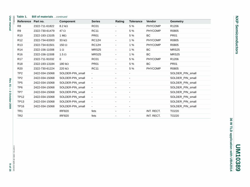
R8 2322-711-61822 8.2 kΩ RC01 - 5 % PHYCOMP R1206
05
1
05
05
25
25
06
1
05
DER_PIN_small
DER_PIN_small
DER_PIN_small
DER_PIN_small
DER_PIN_small
DER_PIN_small
DER_PIN_small
DER_PIN_small
20
20
Table 1. Bill of materials …continued
Reference Part no. Component Series Rating Tolerance Vendor Geometry
© N
XP B
.V. 2009. All rights reserved.
R9 2322-730-61479 47 Ω RC11 - 5 % PHYCOMP R08
R10 2322-193-13105 1 MΩ PR01 - 5 % BC PR0
R12 2322-734-63303 33 kΩ RC12H - 1 % PHYCOMP R08
R13 2322-734-61501 150 Ω RC12H - 1 % PHYCOMP R08
R14 2322-156-11008 1 Ω MRS25 - 1 % BC MRS
R16 2322-156-11508 1.5 Ω MRS25 - 1 % BC MRS
R17 2322-711-91032 0 RC01 - 5 % PHYCOMP R12
R18 2322-193-13184 180 kΩ PR01 - 5 % BC PR0
R20 2322-730-61224 220 kΩ RC11 - 5 % PHYCOMP R08
TP2 2422-034-15068 SOLDER-PIN_small - - - SOL
TP2 2422-034-15068 SOLDER-PIN_small - - - SOL
TP5 2422-034-15068 SOLDER-PIN_small - - - SOL
TP6 2422-034-15068 SOLDER-PIN_small - - - SOL
TP7 2422-034-15068 SOLDER-PIN_small - - - SOL
TP12 2422-034-15068 SOLDER-PIN_small - - - SOL
TP13 2422-034-15068 SOLDER-PIN_small - - - SOL
TP16 2422-034-15068 SOLDER-PIN_small - - - SOL
TR1 IRF820 fets - - INT. RECT. TO2
TR2 IRF820 fets - - INT. RECT. TO2

NXP Semiconductors UM1038936 W TLD application with UBA2014
4. Lamp circuit operation and dimensioning
In this chapter a description will be given how the lamp circuit for a 36 W TLD lamp can be dimensioned. It is assumed that the supply of 400 V is constant and that typical working frequency ftyp is equal to 45 kHz. The RMS value of the half bridge voltage Vhb using the first harmonic approximation can be calculated with Equation 1:
(1)
The minimum frequency is determined by R12 and C14 (see also the UBA2014 data sheet). Equation 2 shows the calculation of fmax:
(2)
As a result the maximum frequency is equal to (Equation 3):
(3)
During the start-up phase the working frequency starts at the maximum frequency. As the load on the half bridge circuit consists of the series connected LC circuit, this is a safe frequency at which currents and voltages are low. The electrodes must be preheated to secure a long lifetime and an efficient ignition of the lamp. During the preheating phase the preheat timer determines the preheating time (Equation 4):
(4)
The preheating current Iph, which flows through the electrodes and the lamp capacitor, is controlled by the preheating current sensor circuit (PCS, pin 8 of the controller, see Figure 4) and is determined by R14, R13, and R9. If the voltage on pin 8 reaches 0.6 V, which means the current has a (peak) value of 0.788 A, the controller enters the preheat state. The RMS value of the preheat current Iph is 0.56 A then. As the lamp voltage and lamp current of the 36 W TLD lamp are known (Vlamp = 102 V, Ilamp = 0.32 A, Rlamp = 319 Ω, and 0.52 A < Iph < 0.96 A at Tph = 1.85 s), one can define the transfer ration in burning condition with Equation 5:
(5)
L1 and C22 are the missing parameters. For the required transfer ratio many combinations for L1 and C22 will do. Choosing a (standard E12) value for C22, like 8.2 nF, L1 can be calculated with 1.9 mH as result. The next step is to define the preheat frequency with these components, which must be higher than the minimum frequency. The preheat voltage has to be calculated also to prevent the lamp from igniting too early.
During preheating, the transfer is only determined by L1 and C22, because the lamp has not ignited yet. Defining of some equations:
Vhb2π
------- 400 V 180 V=⋅=
fmin 1.2 10 2– R12 C14 40 kHz=⋅ ⋅ ⋅=
fmax 2.5 fmin 100 kHz=⋅=
tph 1.7 10 4– R12 C12 1.85 s=⋅ ⋅ ⋅=
HVlampVhb
-------------Rlamp
Rlamp ω2 L1 C22 Rlamp⋅ ⋅ ⋅–( )2
ω L1⋅( )2+
--------------------------------------------------------------------------------------------------------------- 0.57= = =
with ω 2 π ftyp⋅ ⋅=
UM10389_1 © NXP B.V. 2009. All rights reserved.
User manual Rev. 01 — 2 October 2009 10 of 16

NXP Semiconductors UM1038936 W TLD application with UBA2014
The resonance frequency of L1 and C22 (Equation 6):
(6)
Characteristic impedance (Equation 7):
(7)
Frequency deviation (Equation 8):
(8)
Transfer ratio during preheat (Equation 9):
(9)
Then yields (Equation 10):
(10)
For the preheat current yields (Equation 11):
(11)
Filling in the known values for Iph, Z0 and Vhb yields (Equation 12):
(12)
This equation has two solutions (Equation 13 and Equation 14):
(13)
(14)
Solving this two equations give four results for Δ. Keeping in mind that Δ is the ratio between ωph and ω0 and that ph > 0 (inductive mode), the result is a value of 1.39. So,
.
ω01
L1 C22⋅-------------------------=
and f0ω0
2 π⋅----------=
Z0L1
C22----------=
Δωphω0---------=
HphVphVhb----------- 1
1 ωph2 L1 C22⋅ ⋅–
---------------------------------------------- 11 Δ2 ω0
2 L1 C22⋅ ⋅ ⋅–------------------------------------------------------= = =
Vph1
1 Δ2–
------------------ Vhb⋅=
Iphj ωph C22⋅ ⋅
1 ωph2 L1 C22⋅ ⋅–
---------------------------------------------- Vhbj Δ⋅
1 Δ2–
---------------VhbZ0--------⋅=⋅=
IphZ0Vhb--------⋅ Δ
Δ2------ 1.5= =
Δ
1 Δ2–
--------------- 1.5=
Δ
Δ2 1–--------------- 1.5=
fph 1.39 f0 55.6 kHz=⋅=
UM10389_1 © NXP B.V. 2009. All rights reserved.
User manual Rev. 01 — 2 October 2009 11 of 16

NXP Semiconductors UM1038936 W TLD application with UBA2014
The other solutions for are 0.72 (capacitive mode) and −0.72 and −1.39 (theoretically possible, but negative frequencies do not exist).
The preheat voltage then is (Equation 15):
(15)
or a 273 V peak (see Figure 6) low enough to prevent early ignition (the minimum ignition voltage for a TLD36W is 290 V (RMS)).
During the ignition phase the working frequency is decreased because of the charging of C13 by an internally fixed current. During this continuously decrease in frequency, the circuit approaches the resonance frequency f0 of the ballast coil and lamp capacitor (40 kHz). The ignition voltage of the lamp is designed above the Vlampfail level. If the lamp voltage passes the Vlampfail level the ignition timer is started. If the preheating of the electrodes was correct, the increasing voltage across the lamp will ignite it. Because of the ignited lamp, the voltage across the lamp will drop below the Vlampfail level and the ignition timer will stop. The frequency will further decrease until the minimum frequency is reached. Then the lamp is ignited and the burn state begins. If, however, at the end of the ignition time the lamp voltage still exceeds the lamp fail level (Vlamp > Vlampfail), then the assumption is that the lamp has not ignited and the IC enters the power-down state.
During the ignition of the lamp and the burn phase the capacitive mode protection (ACM) ensures a safe operation of the power MOSFETs. However, the ignition voltage increases with the ageing of the lamp. To avoid overload of the key components, the maximum ignition voltage (Vlampmax) is limited and controlled by the LVS circuit (pin 13). The maximum ignition time, in which the lamp should ignite, is determined by (Equation 16):
(16)
In the burn state the ACS of the UBA2014 controls the lamp current. As the system efficiency is high, the lamp power (Plamp) is almost equal to input power. As the 400 V supply voltage is constant, Plamp can be kept constant by controlling the averaged voltage across resistor R14. In this way the lamp current is controlled.
Dimming is performed by changing the reference level at the CSP pin (pin 15) by turning potentiometer R4. In this way the input voltage of the voltage controlled oscillator regulates the frequency and so indirectly also the lamp current.
The start-up current for the UBA2014 is derived from the 400 V via R1, R10, and one of the lamp electrodes. If the lamp is not present, the IC will not start-up. As soon as VDDhigh is exceeded the IC starts oscillating. The half bridge voltage Vhb (approximately 180 V) together with dv/dt capacitors behave like a current source, which supplies not only the IC and the gates of the MOSFETs but also generates a stable 12 V supply.
More information about the controller can be found in the UBA2014 data sheet. For more information about HF driving the 36 W T8 lamp see IEC60081 sheet 7420.
Vph1
1 1.392–
------------------------ Vbh 193 V=⋅=
tign 3.1 10 5– R12 C12⋅ ⋅ ⋅=
UM10389_1 © NXP B.V. 2009. All rights reserved.
User manual Rev. 01 — 2 October 2009 12 of 16

NXP Semiconductors UM1038936 W TLD application with UBA2014
5. Quick measurements
Fig 6. Ielectrode (1) and Vlamp (3) during start-up and preheat phase (273 V peak)
Fig 7. Vlamp during the preheat, ignition, and burn phase
UM10389_1 © NXP B.V. 2009. All rights reserved.
User manual Rev. 01 — 2 October 2009 13 of 16

NXP Semiconductors UM1038936 W TLD application with UBA2014
The lamp voltage is controlled at the calculated Vlampmax level. After 20 ms the lamp ignites and we see the transition to the burn phase. If the lamp does not ignite at the end of the ignition time, the IC enters power-down state.
Fig 8. Vlamp during the ignition phase
UM10389_1 © NXP B.V. 2009. All rights reserved.
User manual Rev. 01 — 2 October 2009 14 of 16

NXP Semiconductors UM1038936 W TLD application with UBA2014
6. Legal information
6.1 DefinitionsDraft — The document is a draft version only. The content is still under internal review and subject to formal approval, which may result in modifications or additions. NXP Semiconductors does not give any representations or warranties as to the accuracy or completeness of information included herein and shall have no liability for the consequences of use of such information.
6.2 DisclaimersGeneral — Information in this document is believed to be accurate and reliable. However, NXP Semiconductors does not give any representations or warranties, expressed or implied, as to the accuracy or completeness of such information and shall have no liability for the consequences of use of such information.
Right to make changes — NXP Semiconductors reserves the right to make changes to information published in this document, including without limitation specifications and product descriptions, at any time and without notice. This document supersedes and replaces all information supplied prior to the publication hereof.
Suitability for use — NXP Semiconductors products are not designed, authorized or warranted to be suitable for use in medical, military, aircraft, space or life support equipment, nor in applications where failure or malfunction of a NXP Semiconductors product can reasonably be expected to result in personal injury, death or severe property or environmental damage. NXP Semiconductors accepts no liability for inclusion and/or use of NXP Semiconductors products in such equipment or applications and therefore such inclusion and/or use is at the customer’s own risk.
Applications — Applications that are described herein for any of these products are for illustrative purposes only. NXP Semiconductors makes no representation or warranty that such applications will be suitable for the specified use without further testing or modification.
Export control — This document as well as the item(s) described herein may be subject to export control regulations. Export might require a prior authorization from national authorities.
6.3 TrademarksNotice: All referenced brands, product names, service names and trademarks are the property of their respective owners.
UM10389_1 © NXP B.V. 2009. All rights reserved.
User manual Rev. 01 — 2 October 2009 15 of 16
NXP Semiconductors UM1038936 W TLD application with UBA2014
7. Contents
1 Introduction . . . . . . . . . . . . . . . . . . . . . . . . . . . . 32 Features . . . . . . . . . . . . . . . . . . . . . . . . . . . . . . . 43 General description . . . . . . . . . . . . . . . . . . . . . . 43.1 Printed-circuit board . . . . . . . . . . . . . . . . . . . . . 43.2 Block diagram. . . . . . . . . . . . . . . . . . . . . . . . . . 53.3 Circuit diagram . . . . . . . . . . . . . . . . . . . . . . . . . 73.4 Bill of materials . . . . . . . . . . . . . . . . . . . . . . . . . 84 Lamp circuit operation and dimensioning . . 105 Quick measurements. . . . . . . . . . . . . . . . . . . . 136 Legal information. . . . . . . . . . . . . . . . . . . . . . . 156.1 Definitions. . . . . . . . . . . . . . . . . . . . . . . . . . . . 156.2 Disclaimers . . . . . . . . . . . . . . . . . . . . . . . . . . . 156.3 Trademarks. . . . . . . . . . . . . . . . . . . . . . . . . . . 157 Contents . . . . . . . . . . . . . . . . . . . . . . . . . . . . . . 16
© NXP B.V. 2009. All rights reserved.For more information, please visit: http://www.nxp.comFor sales office addresses, please send an email to: [email protected]
Date of release: 2 October 2009Document identifier: UM10389_1
Please be aware that important notices concerning this document and the product(s)described herein, have been included in section ‘Legal information’.